ADM1024 - System Hardware Monitor with Remote Diode Thermal ...
30
© Semiconductor Components Industries, LLC, 2016 January, 2016 - Rev. 5 1 Publication Order Number: ADM1024/D ADM1024 System Hardware Monitor with Remote Diode Thermal Sensing The ADM1024 is a complete system hardware monitor for microprocessor-based systems, providing measurement and limit comparison of various system parameters. Eight measurement inputs are provided; three are dedicated to monitoring 5.0 V and 12 V power supplies and the processor core voltage. The ADM1024 can monitor a fourth power supply voltage by measuring its own V CC . One input (two pins) is dedicated to a remote temperature-sensing diode. Two more pins can be configured as inputs to monitor a 2.5 V supply and a second processor core voltage, or as a second temperature-sensing input. The remaining two inputs can be programmed as general purpose analog inputs or as digital fan speed measuring inputs. Measured values can be read out via a serial System Management Bus and values for limit comparisons can be programmed in over the same serial bus. The high speed successive approximation ADC allows frequent sampling of all analog channels to ensure a fast interrupt response to any out-of-limit measurement. The ADM1024’s 2.8 V to 5.5 V supply voltage range, low supply current, and SMBus interface make it ideal for a wide range of applications. These include hardware monitoring and protection applications in personal computers, electronic test equipment, and office electronics. Features • Up to Nine Measurement Channels • Inputs Programmable-to-Measure Analog Voltage, Fan Speed or External Temperature • External Temperature Measurement with Remote Diode (Two Channels) • On-chip Temperature Sensor • Five Digital Inputs for VID Bits • LDCM Support • System Management Bus (SMBus) • Chassis Intrusion Detect • Interrupt and Overtemperature Outputs • Programmable RESET Input Pin • Shutdown Mode to Minimize Power Consumption • Limit Comparison of All Monitored Values • This is a Pb-Free Device* Applications • Network Servers and Personal Computers • Microprocessor-Based Office Equipment • Test Equipment and Measuring Instruments *For additional information on our Pb-Free strategy and soldering details, please download the ON Semiconductor Soldering and Mounting Techniques Reference Manual, SOLDERRM/D. www. onsemi.com See detailed ordering and shipping information in the package dimensions section on page 29 of this data sheet. ORDERING INFORMATION YY = Year WW = Work Week ZZZZ = Assembly Lot Number CCCC = Country of Origin MARKING DIAGRAM TSSOP-24 CASE 948H ADM 1024 ARUZ 1 PIN ASSIGNMENT AD1024 (Top View) VID0/IRQ0 VID1/IRQ1 VID2/IRQ2 VID3/IRQ3 VID4/IRQ4 +V CCP1 +2.5V IN /D2+ V CCP2 /D2- +5.0V IN +12V IN D1+ D1- NTEST_OUT/ADD THERM SDA SCL FAN1/AIN1 FAN2/AIN2 CI GND V CC INT NTEST_IN/AOUT RESET 24 1 23 2 22 3 21 4 20 5 19 6 18 7 17 8 16 9 15 10 14 11 13 12 #YYWW ZZZZZZZZZ CCCCCCCCCCC Top Marking Bottom Marking
-
Upload
truongminh -
Category
Documents
-
view
221 -
download
0
Transcript of ADM1024 - System Hardware Monitor with Remote Diode Thermal ...

© Semiconductor Components Industries, LLC, 2016
January, 2016 − Rev. 51 Publication Order Number:
ADM1024/D
ADM1024
System Hardware Monitorwith Remote Diode ThermalSensing
The ADM1024 is a complete system hardware monitor formicroprocessor-based systems, providing measurement and limitcomparison of various system parameters. Eight measurement inputsare provided; three are dedicated to monitoring 5.0 V and 12 V powersupplies and the processor core voltage. The ADM1024 can monitor afourth power supply voltage by measuring its own VCC. One input(two pins) is dedicated to a remote temperature-sensing diode. Twomore pins can be configured as inputs to monitor a 2.5 V supply and asecond processor core voltage, or as a second temperature-sensinginput. The remaining two inputs can be programmed as generalpurpose analog inputs or as digital fan speed measuring inputs.Measured values can be read out via a serial System Management Busand values for limit comparisons can be programmed in over the sameserial bus. The high speed successive approximation ADC allowsfrequent sampling of all analog channels to ensure a fast interruptresponse to any out-of-limit measurement.
The ADM1024’s 2.8 V to 5.5 V supply voltage range, low supplycurrent, and SMBus interface make it ideal for a wide range ofapplications. These include hardware monitoring and protectionapplications in personal computers, electronic test equipment, and officeelectronics.
Features• Up to Nine Measurement Channels
• Inputs Programmable-to-Measure Analog Voltage,Fan Speed or External Temperature
• External Temperature Measurement with Remote Diode(Two Channels)
• On-chip Temperature Sensor
• Five Digital Inputs for VID Bits
• LDCM Support
• System Management Bus (SMBus)
• Chassis Intrusion Detect
• Interrupt and Overtemperature Outputs
• Programmable RESET Input Pin
• Shutdown Mode to Minimize Power Consumption
• Limit Comparison of All Monitored Values
• This is a Pb-Free Device*
Applications• Network Servers and Personal Computers
• Microprocessor-Based Office Equipment
• Test Equipment and Measuring Instruments
*For additional information on our Pb−Free strategy and soldering details, pleasedownload the ON Semiconductor Soldering and Mounting TechniquesReference Manual, SOLDERRM/D.
www.onsemi.com
See detailed ordering and shipping information in the packagedimensions section on page 29 of this data sheet.
ORDERING INFORMATION
YY = YearWW = Work WeekZZZZ = Assembly Lot NumberCCCC = Country of Origin
MARKING DIAGRAM
TSSOP−24CASE 948H
ADM1024ARUZ
1
PIN ASSIGNMENT
AD1024(Top View)
VID0/IRQ0
VID1/IRQ1
VID2/IRQ2
VID3/IRQ3
VID4/IRQ4
+VCCP1
+2.5VIN/D2+
VCCP2/D2−
+5.0VIN
+12VIN
D1+
D1−
NTEST_OUT/ADD
THERM
SDA
SCL
FAN1/AIN1
FAN2/AIN2
CI
GND
VCC
INT
NTEST_IN/AOUT
RESET
241
232
223
214
205
196
187
178
169
1510
1411
1312
#YYWWZZZZZZZZZ
CCCCCCCCCCC
Top Marking
Bottom Marking

ADM1024
www.onsemi.com2
Figure 1. Functional Block Diagram
10−BIT ADC
D1+
D1–
GND
ADM1024
CI
VID0/IRQ0
VID1/IRQ1
VID2/IRQ2
VID3/IRQ3
VID4/IRQ4
FAN1/AIN1
FAN2/AIN2
POWER TO CHIP
+VCCP1
+2.5VIN/D2+
+5.0VIN
+12VIN
VCCP2/D2–
VCC
PULLUPS
VCC
VID0–3 ANDFAN DIVISOR
REGISTER
VID4 ANDDEVICE IDREGISTER
FAN SPEEDCOUNTER
INPUTATTENUATORS
ANDANALOG
MULTIPLEXER
BAND GAPTEMPERATURE
SENSOR
ADDRESSPOINTER
REGISTER
TEMPERATURECONFIGURATION
REGISTER
2.5VBAND GAP
REFERENCE
SERIAL BUSINTERFACE
CHANNELMODE
REGISTER
VALUE ANDLIMIT
REGISTERS
LIMITCOMPARATORS
INTERRUPTSTATUS
REGISTERS
INT MASKREGISTERS
INTERRUPTMASKING
CONFIGURATIONREGISTERS
ANALOGOUTPUT
REGISTER AND8−BIT DAC
NTEST_OUT/ADD
INT
NTEST_IN/AOUT
THERM
RESET
VCC
VCC
VCC
100k
CHASSISINTRUSION
CLEARREGISTER
SDA
SCL
100k
100k
100k
Table 1. ABSOLUTE MAXIMUM RATINGS
Parameter Rating Unit
Positive Supply Voltage (VCC) 6.5 V
Voltage on 12 VIN Pin 20 V
Voltage on AOUT, NTEST_OUT ADD, 2.5 VIN/D2+ −0.3 to (VCC + 0.3) V
Voltage on Any Other Input or Output Pin −0.3 to +6.5 V
Input Current at Any Pin ±5 mA
Package Input Current ±20 mA
Maximum Junction Temperature (TJMAX) 150 °C
Storage Temperature Range −65 to +150 °C
Lead Temperature, SolderingReflow Temperature 260
°C
ESD Rating All Pins 2000 V
Stresses exceeding those listed in the Maximum Ratings table may damage the device. If any of these limits are exceeded, device functionalityshould not be assumed, damage may occur and reliability may be affected.NOTE: This device is ESD sensitive. Use standard ESD precautions when handling.
Table 2. THERMAL CHARACTERISTICS
Package Type JA JC Unit
24-Lead Small Outline Package 50 10 °C/W

ADM1024
www.onsemi.com3
Table 3. PIN ASSIGNMENT
Pin No. Mnemonic Description
1 NTEST_OUT/ADD Digital I/O. Dual function pin. This is a three-state input that controls the two LSBs of the Serial BusAddress. This pin functions as an output when doing a NAND test.
2 THERM Digital I/O. Dual function pin. This pin functions as an interrupt output for temperature interrupts only, oras an interrupt input for fan control. It has an on-chip 100 k pullup resistor.
3 SDA Digital I/O. Serial bus bidirectional data. Open-drain output.
4 SCL Digital Input. Serial bus clock.
5 FAN1/AIN1 Programmable Analog/Digital Input. 0 V to 2.5 V analog input or digital (0 to VCC) amplitude fantachometer input.
6 FAN2/AIN2 Programmable Analog/Digital Input. 0 V to 2.5 V analog input or digital (0 to VCC) amplitude fantachometer input.
7 CI Digital I/O. An active high input from an external latch that captures a Chassis Intrusion event. This linecan go high without any clamping action, regardless of the powered state of the ADM1024. TheADM1024 provides an internal open drain on this line, controlled by Bit 6 of Register 40h or Bit 7 ofRegister 46h, to provide a minimum 20 ms pulse on this line to reset the external Chassis Intrusion Latch.
8 GND System Ground.
9 VCC Power (2.8 V to 5.5 V). Typically powered from 3.3 V power rail. Bypass with the parallel combination of10 F (electrolytic or tantalum) and 0.1 F (ceramic) bypass capacitors.
10 INT Digital Output. Interrupt request (open-drain). The output is enabled when Bit 1 of Register 40h is set to 1.The default state is disabled. It has an on-chip 100 k pullup resistor.
11 NTEST_IN/AOUT Digital Input/Analog Output. An active-high input that enables NAND Test mode board-level connectivitytesting. Refer to the section on NAND testing. Also functions as a programmable analog output whenNAND Test is not selected.
12 RESET Digital I/O. Master Reset, 5 mA driver (open drain), active low output with a 45 ms minimum pulse width.Set using Bit 4 in Register 40h. Also acts as reset input when pulled low (e.g., power-on reset). It has anon-chip 100 k pullup resistor.
13 D1− Analog Input. Connected to cathode of first external temperature-sensing diode.
14 D1+ Analog Input. Connected to anode of first external temperature-sensing diode.
15 +12 VIN Programmable Analog Input. Monitors 12 V supply.
16 +5.0 VIN Analog Input. Monitors 5.0 V supply.
17 VCCP2/D2– Programmable Analog Input. Monitors second processor core voltage or cathode of second externaltemperature-sensing diode.
18 +2.5 VIN/D2+ Programmable Analog Input. Monitors 2.5 V supply or anode of second external temperature-sensingdiode.
19 +VCCP1 Analog Input. Monitors first processor core voltage (0 V to 3.6 V).
20 VID4/IRQ4 Digital Input. Core Voltage ID readouts from the processor. This value is read into the VID4 StatusRegister. Can also be reconfigured as an interrupt input. It has an on-chip 100 k pullup resistor.
21 VID3/IRQ3 Digital Input. Core Voltage ID readouts from the processor. This value is read into the VID0–VID3 StatusRegister. Can also be reconfigured as an interrupt input. It has an on-chip 100 k pullup resistor.
22 VID2/IRQ2 Digital Input. Core Voltage ID readouts from the processor. This value is read into the VID0–VID3 StatusRegister. Can also be reconfigured as an interrupt input. It has an on-chip 100 k pullup resistor.
23 VID1/IRQ1 Digital Input. Core Voltage ID readouts from the processor. This value is read into the VID0–VID3 StatusRegister. Can also be reconfigured as an interrupt input. It has an on-chip 100 k pullup resistor.
24 VID0/IRQ0 Digital Input. Core Voltage ID readouts from the processor. This value is read into the VID0–VID3 StatusRegister. Can also be reconfigured as an interrupt input. It has an on-chip 100 k pullup resistor.

ADM1024
www.onsemi.com4
Table 4. ELECTRICAL CHARACTERISTICS (TA = TMIN to TMAX, VCC = VMIN to VMAX, unless otherwise noted. (Note 1 and 2))
Parameter Test Conditions/Comments Min Typ Max Unit
POWER SUPPLY
Supply Voltage, VCC 2.8 3.3 5.5 V
Supply Current, ICC Interface Inactive, ADC ActiveADC Inactive, DAC ActiveShutdown Mode
−−−
1.41.045
3.5−
145
mA
A
TEMPERATURE-TO-DIGITAL CONVERTER
Internal Sensor Accuracy 0°C ≤ TA ≤ 100°CTA = 25°C
−−
−−
±3.0±2.0
°C
Resolution − ±1.0 − °C
External Diode Sensor Accuracy 0°C ≤ TA ≤ 100°C25°C
−−
−±3.0
±5.0−
°C
Resolution − ±1.0 − °C
Remote Sensor Source Current High levelLow level
804.0
1106.5
1509.0
A
ANALOG-TO-DIGITAL CONVERTER (Including MUX and ATTENUATORS)
Total Unadjusted Error (TUE) (12 VIN) (Note 3) − − ±4.0 %
TUE (AIN, VCCP, 2.5 VIN, 5.0 VIN) − − ±3.0 %
Differential Non-linearity (DNL) − − ±1.0 LSB
Power Supply Sensitivity − ±1.0 − %/V
Conversion Time(Analog Input or Internal Temperature)
(Note 4) − 754.8 856.8 s
Conversion Time (External Temperature) (Note 4) − 9.6 − ms
Input Resistance (2.5 V, 5.0 V, 12 V, VCCP1, VCCP2) 80 140 200 k
Input Resistance (AIN1, AIN2) − 5.0 − M
ANALOG OUTPUT
Output Voltage Range 0 − 2.5 V
Total Unadjusted Error (TUE) IL = 2 mA − − ±3.0 %
Full-Scale Error − ±1.0 ±5.0 %
Zero-Scale Error No Load − 2.0 − LSB
Differential Non-linearity (DNL) Monotonic by Design − − ±1.0 LSB
Integral Non-linearity − ±1.0 − LSB
Output Source Current − 2.0 − mA
Output Sink Current − 1.0 − mA
FAN RPM-TO-DIGITAL CONVERTER
Accuracy 0°C ≤ TA ≤ 100°C − − ±12 %
Full-Scale Count − − 255
FAN1 to FAN2 Nominal Input RPM (Note 5) Divisor = 1, Fan Count = 153Divisor = 2, Fan Count = 153Divisor = 3, Fan Count = 153Divisor = 4, Fan Count = 153
−−−−
8800440022001100
−−−−
RPM
Internal Clock Frequency 0°C ≤ TA ≤ 100°C 19.8 22.5 25.2 kHz
DIGITAL OUTPUTS (NTEST_OUT)
Output High Voltage, VOH IOUT = +3.0 mA, VCC = 2.85 V −3.60 V 2.4 − − V
Output Low Voltage, VOL IOUT = −3.0 mA, VCC = 2.85 V −3.60 V − − 0.4 V
OPEN-DRAIN DIGITAL OUTPUTS (INT, THERM, RESET) (Note 6)
Output Low Voltage, VOL IOUT = 3.0 mA, VCC = 3.60 V − − 0.4 V
High Level Output Leakage Current, IOH VOUT = VCC − 0.1 100 A
RESET and CI Pulsewidth 20 45 − ms
ADM1024
www.onsemi.com5
Table 4. ELECTRICAL CHARACTERISTICS (TA = TMIN to TMAX, VCC = VMIN to VMAX, unless otherwise noted. (Note 1 and 2))
Parameter UnitMaxTypMinTest Conditions/Comments
OPEN-DRAIN SERIAL DATABUS OUTPUT (SDA)
Output Low Voltage, VOL IOUT = −3.0 mA, VCC = 2.85 V −3.60 V − − 0.4 V
High Level Output Leakage Current, IOH VOUT = VCC − 0.1 100 A
SERIAL BUS DIGITAL INPUTS (SCL, SDA)
Input High Voltage, VIH 2.2 − − V
Input Low Voltage, VIL − − 0.8 V
Hysteresis − 500 − mV
Glitch Immunity − 100 − ns
DIGITAL INPUT LOGIC LEVELS (ADD, CI, RESET, VID0−VID4, FAN1, FAN2) (Note 7)
Input High Voltage, VIH VCC = 2.85 V − 5.5 V 2.2 − − V
Input Low Voltage, VIL VCC = 2.85 V − 5.5 V − − 0.8 V
NTEST_IN
Input High Current, IIH VCC = 2.85 V − 5.5 V 2.2 − − V
DIGITAL INPUT CURRENT
Input High Current, IIH VIN = VCC –1.0 − − A
Input Low Current, IIL VIN = 0 − − 1.0 A
Input Capacitance, CIN − 20 − pF
SERIAL BUS TIMING (Note 8)
Clock Frequency, fSCLK See Figure 2 − − 400 kHz
Glitch Immunity, tSW See Figure 2 − − 50 ns
Bus Free Time, tBUF See Figure 2 1.3 − − s
Start Setup Time, tSU; STA See Figure 2 600 − − ns
Start Hold Time, tHD; STA See Figure 2 600 − − ns
SCL Low Time, tLOW See Figure 2 1.3 − − s
SCL High Time, tHIGH See Figure 2 0.6 − − s
SCL, SDA Rise Time, tr See Figure 2 − − 300 ns
SCL, SDA Fall Time, tf See Figure 2 − − 300 s
Data Setup Time, tSU; DAT See Figure 2 100 − − ns
Data Hold Time, tHD; DAT See Figure 2 − − 900 ns
1. All voltages are measured with respect to GND, unless otherwise specified.2. Typicals are at TA = 25°C and represent the most likely parametric norm. Shutdown current typ is measured with VCC = 3.3V.3. TUE (Total Unadjusted Error) includes Offset, Gain, and Linearity errors of the ADC, multiplexer, and on-chip input attenuators, including
an external series input protection resistor value between 0 k and 1 k.4. Total monitoring cycle time is nominally m × 755 s + n × 33244 s, where m is the number of channels configured as analog inputs, plus 2
for the internal VCC measurement and internal temperature sensor, and n is the number of channels configured as external temperaturechannels (D1 and D2).
5. The total fan count is based on two pulses per revolution of the fan tachometer output.6. Open−drain digital outputs may have an external pullup resistor connected to a voltage lower or higher than VCC (up to 6.5 V absolute maximum).7. All logic inputs except ADD are tolerant of 5.0 V logic levels, even if VCC is less than 5.0 V. ADD is a three-state input that may be connected
to VCC, GND, or left open−circuit.8. Timing specifications are tested at logic levels of VIL = 0.8 V for a falling edge and VIH = 2.2 V for a rising edge.
Figure 2. Serial Bus Timing Diagram
PSP S
SCL
SDA
tR tF
tLOW
tHD:STA
tHD:DATtHIGH tSU:DAT
tSU:STA
tHD:STA
tSU:STO
tBUF
ADM1024
www.onsemi.com6
TYPICAL PERFORMANCE CHARACTERISTICS
Figure 3. Temperature Error vs. PC BoardTrack Resistance
Figure 4. Temperature Error vs. Power SupplyNoise Frequency
Figure 5. Temperature Error vs. Common-modeNoise Frequency
Figure 6. Pentium III Temperature vs. ADM1024Reading
Figure 7. Temperature Error vs. CapacitanceBetween D+ and D–
Figure 8. Temperature Error vs. Differential-modeNoise Frequency
MEASURED TEMPERATURE
RE
AD
ING
0 10 20 30 40 50 60 70 80 90 100 1100
10
20
30
40
50
60
70
80
90
100
110
1 3.3 10 30–60
–50
–40
–30
–20
–10
0
10
20
30
100
LEAK RESISTANCE (MΩ)
TE
MP
ER
AT
UR
E E
RR
OR
(°C
)
DXP TO GND
DXP TO VCC (5.0 V)
50 500 5k 50k–1
0
1
2
3
4
5
6
50M
FREQUENCY (Hz)
TE
MP
ER
AT
UR
E E
RR
OR
(C
)
500k 5M
250mV p−p REMOTE
100mV p−p REMOTE
50 500 5k 50k–5
0
5
10
15
20
25
50M
FREQUENCY (Hz)
TE
MP
ER
AT
UR
E E
RR
OR
(C
)
500k 5M
100mV p−p
50mV p−p
25mV p−p
1 2.2 3.2 4.7–5
0
5
10
15
20
25
10
DXP−DXN CAPACITANCE (nF)
TE
MP
ER
AT
UR
E E
RR
OR
(C
)
7 50 500 5k 50k0
1
2
3
7
8
10
50M
FREQUENCY (Hz)
TE
MP
ER
AT
UR
E E
RR
OR
(C
)
500k 5M 25M100k
4
5
6
9
10mV SQ. WAVE

ADM1024
www.onsemi.com7
TYPICAL PERFORMANCE CHARACTERISTICS
Figure 9. Standby Current vs. Temperature
22.5
23.0
23.5
24.0
26.0
26.5
TEMPERATURE (C)
ST
AN
DB
Y C
UR
RE
NT
(
A)
24.5
25.0
25.5
–40 –20 0 20 40 60 80 100 120
VDD = 3.3 V

ADM1024
www.onsemi.com8
General DescriptionThe ADM1024 is a complete system hardware monitor for
microprocessor-based systems. The device communicateswith the system via a serial SMBus. The serial bus controllerhas a hardwired address line for device selection (Pin 1), aserial data line for reading and writing addresses and data(SDA, Pin 14), and an input line for the serial clock (Pin 3),and an input line for the serial clock (Pin 4). All control andprogramming functions of the ADM1024 are performed overthe serial bus.
Measurement InputsProgrammability of the measurement inputs makes the
ADM1024 extremely flexible and versatile. The device hasa 10−bit ADC and nine measurement input pins that can beconfigured in different ways.
Pins 5 and 6 can be programmed as general-purposeanalog inputs with a range of 0 V to 2.5 V, or as digital inputsto monitor the speed of fans with digital tachometer outputs.The fan inputs can be programmed to accommodate fanswith different speeds and different numbers of pulses perrevolution from their tachometer outputs.
Pins 13 and 14 are dedicated temperature inputs and maybe connected to the cathode and anode of an externaltemperature sensing diode.
Pins 15, 16, and 19 are dedicated analog inputs withon-chip attenuators, configured to monitor 12 V, 5.0 V, andthe processor core voltage, respectively.
Pins 17 and 18 may be configured as analog inputs withon-chip attenuators to monitor a second processor core voltageand a 2.5 V supply, or they may be configured as a temperatureinput and connected to a second temperature-sensing diode.
The ADC also accepts input from an on-chip band gaptemperature sensor that monitors system-ambient temperature.
Finally, the ADM1024 monitors the supply from which itis powered, so there is no need for a separate 3.3 V analoginput if the chip VCC is 3.3 V. The range of this VCCmeasurement can be configured for either a 3.3 V or 5.0 VVCC by Bit 3 of the Channel Mode Register.
Sequential MeasurementWhen the ADM1024 monitoring sequence is started, it
cycles sequentially through the measurement of analoginputs and the temperature sensor, while at the same time thefan speed inputs are independently monitored. Measuredvalues from these inputs are stored in Value Registers. Thesecan be read out over the serial bus, or can be compared withprogrammed limits stored in the Limit Registers. The resultsof out-of-limit comparisons are stored in the Interrupt StatusRegisters, and will generate an interrupt on the INT line(Pin 10).
Any or all of the Interrupt Status Bits can be masked byappropriate programming of the Interrupt Mask Register.
Processor Voltage IDFive digital inputs (VID4 to VID0−Pins 20 to 24) read the
processor voltage ID code. These inputs can also bereconfigured as interrupt inputs.
The VID pins have internal 100 k pullup resistors.
Chassis IntrusionA chassis intrusion input (Pin 7) is provided to detect
unauthorized tampering with the equipment.
RESETA RESET input/output (Pin 12) is provided. Pulling this
pin low will reset all ADM1024 internal registers to defaultvalues. The ADM1024 can also be programmed to give alow going 45 ms reset pulse at this pin.
Analog OutputThe ADM1024 contains an on-chip, 8-bit DAC with an
output range of 0 V to 2.5 V (Pin 11). This is typically usedto implement a temperature-controlled fan by controllingthe speed of a fan dependent upon the temperature measuredby the on-chip temperature sensor.
Testing of board level connectivity is simplified byproviding a NAND tree test function. The AOUT (Pin 11)also doubles as a NAND test input, while Pin 1 doubles asa NAND tree output.
Internal Registers of the ADM1024A brief description of the ADM1024’s principal internal
registers follows. More detailed information on the functionof each register is given in Table 10 to Table 23:• Configuration Registers: Provide control and
configuration.• Channel Mode Register: Stores the data for the
operating modes of the input channels.• Address Pointer Register: This register contains the
address that selects one of the other internal registers.When writing to the ADM1024, the first byte of data isalways a register address, which is written to theAddress Pointer Register.
• Interrupt (INT) Status Registers: Two registers toprovide status of each interrupt event. These registersare also mirrored at addresses 4Ch and 4Dh.
• Interrupt (INT) Mask Registers: Allow masking ofindividual interrupt sources.
• Temperature Configuration Register: The configurationof the temperature interrupt is controlled by the lowerthree bits of this register.
• VID/Fan Divisor Register: The status of the VID0 toVID4 pins of the processor can be written to and readfrom these registers. Divisor values for fan speedmeasurement are also stored in this register.
ADM1024
www.onsemi.com9
• Value and Limit Registers: The results of analogvoltage inputs, temperature, and fan speedmeasurements are stored in these registers, along withtheir limit values.
• Analog Output Register: The code controlling theanalog output DAC is stored in this register.
• Chassis Intrusion Clear Register: A signal latched onthe chassis intrusion pin can be cleared by writing tothis register.
Serial Bus InterfaceControl of the ADM1024 is carried out via the serial bus.
The ADM1024 is connected to this bus as a slave device,under the control of a master device, e.g., ICH.
The ADM1024 has a 7-bit serial bus address. When thedevice is powered up, it will do so with a default serial busaddress. The 5 MSBs of the address are set to 01011, and the2 LSBs are determined by the logical states of Pin 1 (NTESTOUT/ADD). This is a three-state input that can be grounded,connected to VCC, or left open-circuit to give three differentaddresses.
Table 5. ADD PIN TRUTH TABLE
ADD Pin A1 A0
GND 1 0
No Connect 0 0
VCC 0 1
If ADD is left open-circuit, the default address will be0101100. ADD is sampled only at powerup, so any changesmade while power is on will have no immediate effect.
The facility to make hardwired changes to A1 and A0allows the user to avoid conflicts with other devices sharingthe same serial bus, for example, if more than one ADM1024is used in a system.
The serial bus protocol operates as follows:1. The master initiates data transfer by establishing a
START condition, defined as a high-to-lowtransition on the serial data line SDA while theserial clock line, SCL, remains high. This indicatesthat an address/data stream will follow. All slaveperipherals connected to the serial bus respond tothe START condition, and shift in the next eightbits, consisting of a 7-bit address (MSB first) plusan R/W bit, which determines the direction of thedata transfer, i.e., whether data will be written toor read from the slave device.The peripheral whose address corresponds to thetransmitted address responds by pulling the dataline low during the low period before the ninthclock pulse, known as the Acknowledge Bit. Allother devices on the bus now remain idle while theselected device waits for data to be read from orwritten to it. If the R/W bit is a 0, the master willwrite to the slave device. If the R/W bit is a 1, themaster will read from the slave device.
2. Data is sent over the serial bus in sequences ofnine clock pulses, eight bits of data followed by anAcknowledge Bit from the slave device.Transitions on the data line must occur during thelow period of the clock signal and remain stableduring the high period, as a low-to-high transitionwhen the clock is high may be interpreted as aSTOP signal. The number of data bytes that can betransmitted over the serial bus in a single Read orWrite operation is limited only by what the masterand slave devices can handle.
3. When all data bytes have been read or written,stop conditions are established. In Write mode, themaster will pull the data line high during the tenthclock pulse to assert a STOP condition. In Readmode, the master device will override theAcknowledge Bit by pulling the data line highduring the low period before the ninth clock pulse.This is known as No Acknowledge. The masterwill then take the data line low during the lowperiod before the tenth clock pulse, then highduring the tenth clock pulse to assert a STOPcondition.
Any number of bytes of data may be transferred over theserial bus in one operation, but it is not possible to mix readand write in one operation because the type of operation isdetermined at the beginning and cannot subsequently bechanged without starting a new operation.
In the case of the ADM1024, write operations containeither one or two bytes, and read operations contain one byteand perform the following functions.
To write data to one of the device data registers or readdata from it, the Address Pointer Register must be set so thatthe correct data register is addressed, then data can be writteninto that register or read from it. The first byte of a writeoperation always contains an address that is stored in theAddress Pointer Register. If data is to be written to thedevice, the write operation contains a second data byte thatis written to the register selected by the Address PointerRegister. This is illustrated in Figure 10 The device addressis sent over the bus followed by R/W set to 0. This isfollowed by two data bytes. The first data byte is the addressof the internal data register to be written to, which is storedin the Address Pointer Register. The second data byte is thedata to be written to the internal data register.
When reading data from a register, there are twopossibilities:
1. If the ADM1024’s Address Pointer Register valueis unknown or not the desired value, it is firstnecessary to set it to the correct value before datacan be read from the desired data register. This isdone by performing a write to the ADM1024 asbefore, but only the data byte containing theregister address is sent, as data is not to be writtento the register. This is shown in Figure 11.A read operation is then performed consisting of
ADM1024
www.onsemi.com10
the serial bus address, R/W bit set to 1, followedby the data byte read from the data register. This isshown in Figure 12.
2. If the Address Pointer Register is known to bealready at the desired address, data can be read
from the corresponding data register without firstwriting to the Address Pointer Register, soFigure 11 can be omitted.
Figure 10. Writing a Register Address to the Address Pointer Register,then Writing Data to the Selected Register
0
SCL
SDA 1 0 1 1 A1 A0 D7 D6 D5 D4 D3 D2 D1 D0
D0
1 9
SCL (CONTINUED)
SDA (CONTINUED)
ACK. BYADM1024
ACK. BYADM1024
ACK. BYADM1024
START BYMASTER
STOP BYMASTER
FRAME 1SERIAL BUS ADDRESS BYTE
FRAME 2ADDRESS POINTER REGISTER BYTE
FRAME 3DATA BYTE
D1D2D3D4D5D6D7
R/W
1 99 1
Figure 11. Writing to the Address Pointer Register Only
STOP BYMASTER
D0
1 9
D1D2D3D4D5D6D70
SCL
SDA 1 0 1 1 A1 A0
ACK. BYADM1024
ACK. BYADM1024
START BYMASTER
FRAME 1SERIAL BUS ADDRESS BYTE
FRAME 2ADDRESS POINTER REGISTER BYTE
R/W
1 9
Figure 12. Reading Data from a Previously Selected Register
STOP BYMASTER
1 9
SCL
ACK. BYADM1024
START BYMASTER
FRAME 1SERIAL BUS ADDRESS BYTE
1 9
R/W0 1 1 A1 A0 D7 D6 D5 D4 D3 D2 D1 D00 1SDA
NO ACK.BY MASTER
FRAME 2DATA BYTE FROM ADM1024
NOTES1. Although it is possible to read a data byte from a
data register without first writing to the AddressPointer Register, if the Address Pointer Register isalready at the correct value, it is not possible towrite data to a register without writing to theAddress Pointer Register because the first databyte of a write is always written to the AddressPointer Register.
2. In Figure 10 to Figure 12, the serial bus address isshown as the default value 01011(A1)(A0), whereA1 and A0 are set by the three−state ADD pin.
Measurement InputsThe ADM1024 has nine external measurement pins that can
be configured to perform various functions by programmingthe Channel Mode Register.

ADM1024
www.onsemi.com11
Pins 13 and 14 are dedicated to temperature measurement,while Pins 15, 16, and 19 are dedicated analog input channels.Their function is unaffected by the Channel Mode Register.
Pins 5 and 6 can be individually programmed as analoginputs, or as digital fan speed measurement inputs, byprogramming Bits 0 and 1 of the Channel Mode Register.
Bit 3 of the Channel Mode Register configures the internalVCC measurement range for either 3.3 V or 5.0 V.
Bits 4 to 6 of the Channel Mode Register enable or disablePins 22 to 24 when they are configured as interrupt inputs bysetting Bit 7 of the Channel Mode Register. This function iscontrolled for Pins 20 and 21 by Bits 6 and 7 of ConfigurationRegister 2.
Pins 17 and 18 can be configured as analog inputs or as inputsfor external temperature-sensing diodes by programming Bit 2of the Channel Mode Register.
A truth table for the Channel Mode Register is given inTable 6.
Table 6. CHANNEL MODE REGISTER (Note 1)
ChannelMode
Register Bit
ControlsPin(s) Function
0 5 0 = FAN1, 1 = AIN1
1 6 0 = FAN2, 1 = AIN2
2 17, 18 0 = 2.5 V, VCCP2, 1 = D2–, D2+
3 Int. VCCMeas.
0 = 3.3 V, 1 = 5.0 V
4 24 0 = VID0, 1 = IRQ0
5 23 0 = VID1, 1 = IRQ1
6 22 0 = VID2, 1 = IRQ2
7 20–24 0 = VID0 to VID4,1 = Interrupt Inputs
1. Power-on Default = 0000 0000
Table 7. A/D OUTPUT CODE VS. VIN
Input Voltage A/D Output
+12 VIN +5.0 VIN VCC (3.3 V) VCC (5.0 V) +2.5 VIN +VCCP 1/2 AIN (1/2) Decimal Binary
<0.062 <0.026 <0.0172 <0.026 <0.013 <0.014 <0.010 0 00000000
0.062–0.125 0.026–0.052 0.017–0.034 0.026–0.052 0.013–0.026 0.014–0.028 0.010–0.019 1 00000001
0.125–0.188 0.052–0.078 0.034–0.052 0.052–0.078 0.026–0.039 0.028–0.042 0.019–0.029 2 00000010
0.188–0.250 0.078–0.104 0.052–0.069 0.078–0.104 0.039–0.052 0.042–0.056 0.029–0.039 3 00000011
0.250–0.313 0.104–0.130 0.069–0.086 0.104–0.130 0.052–0.065 0.056–0.070 0.039–0.049 4 00000100
0.313–0.375 0.130–0.156 0.086–0.103 0.130–0.156 0.065–0.078 0.070–0.084 0.049–0.058 5 00000101
0.375–0.438 0.156–0.182 0.103–0.120 0.156–0.182 0.078–0.091 0.084–0.098 0.058–0.068 6 00000110
0.438–0.500 0.182–0.208 0.120–0.138 0.182–0.208 0.091–0.104 0.098–0.112 0.068–0.078 7 00000111
0.500–0.563 0.208–0.234 0.138–0.155 0.208–0.234 0.104–0.117 0.112–0.126 0.078–0.087 8 00001000
4.000–4.063 1.666–1.692 1.100–1.117 1.666–1.692
−−−
0.833–0.846 0.900–0.914 0.625–0.63564
(1/4−Scale) 01000000
8.000–8.063 3.330–3.560 2.200–2.217 3.330–3.560
−−−
1.667–1.680 1.800–1.814 1.250–1.260128
(1/2−Scale) 10000000
12.000–12.063 5.000–5.026 3.300–3.317 5.000–5.026
−−−
2.500–2.513 2.700–2.714 1.875–1.885192
(3/4−Scale) 11000000
15.312–15.375 6.380–6.406 4.210–4.230 6.380–6.406
−−−
3.190–3.203 3.445–3.459 2.392–2.402 245 11110101
15.375–15.437 6.406–6.432 4.230–4.245 6.406–6.432 3.203–3.216 3.459–3.473 2.402–2.412 246 11110110
15.437–15.500 6.432–6.458 4.245–4.263 6.432–6.458 3.216–3.229 3.473–3.487 2.412–2.422 247 11110111
15.500–15.563 6.458–6.484 4.263–4.280 6.458–6.484 3.229–3.242 3.487–3.501 2.422–2.431 248 11111000
15.563–15.625 6.484–6.510 4.280–4.300 6.484–6.510 3.242–3.255 3.501–3.515 2.431–2.441 249 11111001
15.625–15.688 6.510–6.536 4.300–4.314 6.510–6.536 3.255–3.268 3.515–3.529 2.441–2.451 250 11111010
15.688–15.750 6.536–6.562 4.314–4.331 6.536–6.562 3.268–3.281 3.529–3.543 2.451–2.460 251 11111011
15.750–15.812 6.562–6.588 4.331–4.348 6.562–6.588 3.281–3.294 3.543–3.558 2.460–2.470 252 11111100
15.812–15.875 6.588–6.615 4.348–4.366 6.588–6.615 3.294–3.307 3.558–3.572 2.470–2.480 253 11111101
ADM1024
www.onsemi.com12
A-to-D ConverterThese inputs are multiplexed into the on-chip, successive
approximation, Analog-to-Digital Converter (ADC). Thishas a resolution of eight bits. The basic input range is 0 V to2.5 V, which is the input range of AIN1 and AIN2, but fiveof the inputs have built-in attenuators to allow measurementof 2.5 V, 5.0 V, 12 V, and the processor core voltages VCCP1and VCCP2 without any external components. To allow forthe tolerance of these supply voltages, the ADC produces anoutput of 3/4 full scale (decimal 192) for the nominal inputvoltage, and so has adequate headroom to cope withovervoltages. Table 7 shows the input ranges of the analoginputs and output codes of the ADC.
When the ADC is running, it samples and converts an inputevery 748 s, except for the external temperature (D1 andD2) inputs. These have special input signal conditioning andare averaged over 16 conversions to reduce noise, and ameasurement on one of these inputs takes nominally 9.6 ms.
Input CircuitsThe internal structure for the analog inputs is shown in
Figure 13. Each input circuit consists of an input protectiondiode, an attenuator, plus a capacitor to form a first-orderlow-pass filter that gives the input immunity to highfrequency noise.
Figure 13. Structure of Analog Inputs
10pF
AIN1–AIN2
35pF
25pF
25pF(SEE TEXT)
50pF
MUX
+12VIN
+5.0VIN
+2.5VIN
+VCCP1/VCCP2
97.3k
42.7k
111.2k
36.7k
55.2k
91.6k
22.7k
122.2k
80k
2.5 V Input PrecautionsWhen using the 2.5 V input, the following precautions
should be noted. There is a parasitic diode between Pin 18and VCC due to the presence of a PMOS current source(which is used when Pin 18 is configured as a temperatureinput). This will become forward biased if Pin 18 is morethan 0.3 V above VCC. Therefore, VCC should never bepowered off with a 2.5 V input connected.
Setting Other Input RangesAIN1 and AIN2 can easily be scaled to voltages other than
2.5 V. If the input voltage range is zero to some positivevoltage, all that is required is an input attenuator, as shownin Figure 14.
Figure 14. Scaling AIN(1−2)
VIN
R1
R2
AIN(1–2)
Negative and bipolar input ranges can be accommodatedby using a positive reference voltage to offset the inputvoltage range so it is always positive.
(eq. 1)R1R2
Vfs
2.52.5
To measure a negative input voltage, an attenuator can beused as shown in Figure 15.
Figure 15. Scaling and Offsetting AIN(1−2)for Negative Inputs
VIN
R1
AIN(1–2)
R2
+VOS
This is a simple and cheap solution, but the followingpoint should be noted. Since the input signal is offset but notinverted, the input range is transposed. An increase in themagnitude of the −12 V supply (going more negative) willcause the input voltage to fall and give a lower output codefrom the ADC. Conversely, a decrease in the magnitude ofthe −12 V supply will cause the ADC code to increase. Themaximum negative voltage corresponds to zero output fromthe ADC. This means that the upper and lower limits will betransposed.
(eq. 2)R1R2
Vfs
VOS
Bipolar input ranges can easily be accommodated. By
making R1 equal to R2 and VOS = 2.5 V, the input range is±2.5 V. Other input ranges can be accommodated by addinga third resistor to set the positive full−scale input voltage.
Figure 16. Scaling and Offsetting AIN(1−2)for Bipolar Inputs
VIN
R1 AIN(1–2)
R2
+VOS
R3
(R3 has no effect as the input voltage at the device pin is zerowhen VIN = minus full scale.)
(eq. 3)R1R2
Vfs
R2
ADM1024
www.onsemi.com13
(R2 has no effect as the input voltage at the device pin is2.5 V when VIN = plus full scale).
R1R3
Vfs
2.52.5
(eq. 4)
Offset voltages other than 2.5 V can be used, but thecalculation becomes more complicated.
Temperature Measurement System
Local Temperature MeasurementThe ADM1024 contains an on-chip band gap temperature
sensor, whose output is digitized by the on-chip ADC. Thetemperature data is stored in the Temperature Value Register(address 27h) and the LSB from Bits 6 and 7 of theTemperature Configuration Register (address 4Bh). As bothpositive and negative temperatures can be measured, thetemperature data is stored in twos complement format, asshown in Table 8. Theoretically, the temperature sensor andADC can measure temperatures from −128°C to +127°Cwith a resolution of 1°C, although temperatures below−40°C and above +125°C are outside the operatingtemperature range of the device.
External Temperature MeasurementThe ADM1024 can measure the temperature of two
external diode sensors or diode-connected transistors,connected to Pins 13 and 14 or 17 and 18.
Pins 13 and 14 are a dedicated temperature input channel.Pins 17 and 18 can be configured to measure a diode sensorby setting Bit 2 of the Channel Mode Register to 1.
The forward voltage of a diode or diode-connectedtransistor, operated at a constant current, exhibits a negativetemperature coefficient of about –2 mV/°C. Unfortunately,the absolute value of VBE varies from device to device, andindividual calibration is required to null this out, so thetechnique is unsuitable for mass production.
The technique used in the ADM1024 is to measure thechange in VBE when the device is operated at two differentcurrents.
This is given by:
(eq. 5)Vbe KTq ln(N)
where:K is Boltzmann’s constant.q is the charge on the carrier.T is the absolute temperature in Kelvins.N is the ratio of the two currents.
Figure 17 shows the input signal conditioning used tomeasure the output of an external temperature sensor. Thisfigure shows the external sensor as a substrate transistorprovided for temperature monitoring on somemicroprocessors, but it could equally well be a discretetransistor.
I
D+
LPF
N I IBIAS
VDD
BIASDIODE
D–
LOW−PASSFILTER
fC = 65kHzVOUT+
VOUT–
TOADCREMOTE
SENSINGTRANSISTOR
Figure 17. Signal Conditioning for External DiodeTemperature Sensors
If a discrete transistor is used, the collector will not begrounded and should be linked to the base. If a PNPtransistor is used, the base is connected to the D− input andthe emitter to the D+ input. If an NPN transistor is used, theemitter is connected to the D− input and the base to the D+input.
To prevent ground noise from interfering with themeasurement, the more negative terminal of the sensor is notreferenced to ground, but is biased above ground by aninternal diode at the D− input. As the sensor is operating ina noisy environment, C1 is provided as a noise filter. See theLayout Considerations section for more information on C1.
To measure VBE, the sensor is switched betweenoperating currents of I and N × I. The resulting waveform ispassed through a 65 kHz low−pass filter to remove noise,then to a chopper−stabilized amplifier that performs thefunctions of amplification and rectification of the waveformto produce a dc voltage proportional to VBE. This voltageis measured by the ADC to give a temperature output in 8-bittwos complement format. To further reduce the effects ofnoise, digital filtering is performed by averaging the resultsof 16 measurement cycles. An external temperaturemeasurement takes nominally 9.6 ms.
The results of external temperature measurements arestored in 8-bit, twos complement format, as illustrated inTable 8.

ADM1024
www.onsemi.com14
Table 8. TEMPERATURE DATA FORMAT
Temperature Digital Output
−128°C 1000 0000
−125°C 1000 0011
−100°C 1001 1100
−75°C 1011 0101
−50°C 1100 1110
−25°C 1110 0111
0°C 0000 0000
+0.5°C 0000 0000
+10°C 0000 1010
+25°C 0001 1001
+50°C 0011 0010
+75°C 0100 1011
+100°C 0110 0100
+125°C 0111 1101
+127°C 0111 1111
Layout ConsiderationsDigital boards can be electrically noisy environments, and
care must be taken to protect the analog inputs from noise,particularly when measuring the very small voltages from aremote diode sensor. The following precautions should betaken:
1. Place the ADM1024 as close as possible to theremote sensing diode. Provided that the worstnoise sources such as clock generators,data/address buses, and CRTs are avoided, thisdistance can be 4 inches to 8 inches.
2. Route the D+ and D− tracks close together, inparallel, with grounded guard tracks on each side.Provide a ground plane under the tracks ifpossible.
3. Use wide tracks to minimize inductance andreduce noise pickup. A 10 mil track minimumwidth and spacing is recommended.
Figure 18. Arrangement of Signal Tracks
10MILGND
D+
GND
D–
10MIL
10MIL
10MIL
10MIL
10MIL
10MIL
10MIL
10MIL
10MIL
10MIL
4. Try to minimize the number of copper/solder joints,which can cause thermocouple effects. Wherecopper/solder joints are used, make sure that theyare in both the D+ and D– path and at the sametemperature. Thermocouple effects should not be amajor problem as 1°C corresponds to about 240V,
and thermocouple voltages are about 3V/°C oftemperature difference. Unless there are twothermocouples with a big temperature differentialbetween them, thermocouple voltages should bemuch less than 200 mV.
5. Place 0.1F bypass and 2200 pF input filtercapacitors close to the ADM1024.
6. If the distance to the remote sensor is more than8 inches, the use of twisted pair cable isrecommended. This will work up to about 6 feet to12 feet.
7. For really long distances (up to 100 feet) useshielded twisted pair such as Belden #8451microphone cable. Connect the twisted pair to D+and D– and the shield to GND close to theADM1024. Leave the remote end of the shieldunconnected to avoid ground loops.
Because the measurement technique uses switchedcurrent sources, excessive cable and/or filter capacitancecan affect the measurement. When using long cables, thefilter capacitor may be reduced or removed.
Cable resistance can also introduce errors. A 1 seriesresistance introduces about 0.5°C error.
Limit ValuesLimit values for analog measurements are stored in the
appropriate limit registers. In the case of voltagemeasurements, high and low limits can be stored so that aninterrupt request will be generated if the measured valuegoes above or below acceptable values. In the case oftemperature, a Hot Temperature or High Limit can beprogrammed, and a Hot Temperature Hysteresis or LowLimit, which will usually be some degrees lower. This canbe useful as it allows the system to be shut down when thehot limit is exceeded, and restarted automatically when it hascooled down to a safe temperature.
Monitoring Cycle TimeThe monitoring cycle begins when a 1 is written to the
Start Bit (Bit 0), and a 0 to the INT_Clear Bit (Bit 3) of theConfiguration Register. INT_Enable (Bit 1) should be set to1 to enable the INT output. The ADC measures each analoginput in turn; as each measurement is completed, the resultis automatically stored in the appropriate value register. This“round robin” monitoring cycle continues until it is disabledby writing a 0 to Bit 0 of the Configuration Register.
As the ADC will normally be left to free-run in thismanner, the time taken to monitor all the analog inputs willnormally not be of interest, as the most recently measuredvalue of any input can be read out at any time.
For applications where the monitoring cycle time isimportant, it can be calculated as follows:
(eq. 6)m t1 n t2
where:
m − the number of inputs configured as analog inputs, plus theinternal VCC measurement and internal temperature sensor.
ADM1024
www.onsemi.com15
t1 − the time taken for an analog input conversion, nominally6.044 ms.n − the number of inputs configured as external temperatureinputs.t2 − the time taken for a temperature conversion, nominally33.24 ms.
This rapid sampling of the analog inputs ensures a quickresponse in the event of any input going out of limits, unlikeother monitoring chips that employ slower ADCs.
Fan Monitoring Cycle TimeWhen a monitoring cycle is started, monitoring of the fan
speed inputs begins at the same time as monitoring of theanalog inputs. However, the two monitoring cycles are notsynchronized in any way. The monitoring cycle time for thefan inputs is dependent on fan speed and is much slower thanfor the analog inputs. For more details, see the Fan SpeedMeasurement section.
Input SafetyScaling of the analog inputs is performed on-chip, so
external attenuators are normally not required. However,since the power supply voltages will appear directly at thepins, it is advisable to add small external resistors in serieswith the supply traces to the chip to prevent damaging thetraces or power supplies should an accidental short such asa probe connect two power supplies together.
As the resistors will form part of the input attenuators,they will affect the accuracy of the analog measurement iftheir value is too high. The analog input channels arecalibrated assuming an external series resistor of 500 , andthe accuracy will remain within specification for any valuefrom 0 k to 1 k, so a standard 510 resistor is suitable.
The worst such accident would be connecting −2.0 V to+12 V, a total of 24 V difference. With the series resistors, thiswould draw a maximum current of approximately 24 mA.
Analog OutputThe ADM1024 has a single analog output from an
unsigned 8-bit DAC that produces 0 V to 2.5 V. The analogoutput register defaults to FF during power-on reset, whichproduces maximum fan speed. The analog output may beamplified and buffered with external circuitry such as an opamp and transistor to provide fan speed control.
Suitable fan drive circuits are given in Figure 19 to Figure 24.When using any of these circuits, the following points should benoted:
1. All of these circuits will provide an output rangefrom 0 V to almost 12 V, apart from Figure 25which loses the base−emitter voltage drop of Q1due to the emitter−follower configuration.
2. To amplify the 2.5 V range of the analog output upto 12 V, the gain of these circuits needs to bearound 4.8.
3. Care must be taken when choosing the op amp toensure that its input common-mode range andoutput voltage swing are suitable.
4. The op amp may be powered from the 12 V railalone or from 12 V. If it is powered from 12 V,then the input common-mode range should includeground to accommodate the minimum outputvoltage of the DAC, and the output voltage shouldswing below 0.6 V to ensure that the transistor canbe turned fully off.
5. If the op amp is powered from −12 V, precautionssuch as a clamp diode to ground may be needed toprevent the base-emitter junction of the outputtransistor being reverse-biased in the unlikelyevent that the output of the op amp should swingnegative for any reason.
Figure 19. Fan Drive Circuit with Op Amp andEmitter-Follower
AOUT
12V
Q12N2219A
1/4LM324
R110kΩ
R236kΩ
Figure 20. Fan Drive Circuit with Op Amp and PNPTransistor
AOUT
12V
Q1BD1362SA968
1/4LM324
R110kΩ
R31kΩ
R239kΩ
R41kΩ
Figure 21. Fan Driver Circuit with Op Amp andP-Channel MOSFET
AOUT
12V
Q1IRF9620
1/4LM324
R110kΩ
R3100kΩ
R239kΩ
ADM1024
www.onsemi.com16
Figure 22. Discrete Fan Drive Circuit with P-ChannelMOSFET, Single Supply
AOUT
12V
Q3IRF9620
R2100kΩ
R33.9kΩ
R41kΩ
R1100kΩ
Q1/Q2MBT3904
DUAL
Figure 23. Discrete Fan Drive Circuit with P-ChannelMOSFET, Dual Supply
AOUT
12V
Q3IRF9620
R2100kΩ
–12V
Q1/Q2MTB3904
DUAL
R339kΩ
R410kΩ
R14.7kΩ
Figure 24. Discrete Fan Drive Circuit with BipolarOutput, Dual Supply
AOUT
12V
R2100kΩ Q4
BD132TIP32AQ3
BC5562N3906
Q1/Q2MBT3904
DUAL
R1100kΩ
R33.9kΩ
R41kΩ
R5100kΩ
6. In all these circuits, the output transistor must havean ICMAX greater than the maximum fan current,and be capable of dissipating power due to thevoltage dropped across it when the fan is notoperating at full speed.
7. If the fan motor produces a large back EMF whenswitched off, it may be necessary to add clampdiodes to protect the output transistors in the eventthat the output goes very quickly from full scale tozero.
Fault-Tolerant Fan ControlThe ADM1024 incorporates a fault-tolerant fan control
capability that can override the setting of the analog outputand force it to maximum to give full fan speed in the eventof a critical overtemperature problem even if, for somereason, this has not been handled by the system software.
There are four temperature set points that will force theanalog output to FFh if any one of them is exceeded for threeor more consecutive measurements. Two of these limits areprogrammable by the user and two are hardware limitsintended as must not exceed limits that cannot be changed.The analog output will be forced to FFh if:
The temperature measured by the on-chip sensor exceedsthe limit programmed into register address 13hp;
or:The temperature measured by either of the remote sensors
exceeds the limit programmed into address 14h;
or:The temperature measured by the on-chip sensor exceeds
70°C, which is hardware programmed into a read-onlyregister at address 17h;
or:The temperature measured by either of the remote sensors
exceeds 85°C, which is hardware programmed into aread-only register at address 18h.
Once the hardware override of the analog output istriggered, it will return to normal operation only after threeconsecutive measurements that are 5 degrees lower thaneach of the above limits.
The analog output can also be forced to FFh by pulling theTHERM pin (Pin 2) low.
The limits in Registers 13h and 14h can be programmedby the user. Obviously, these limits should not exceed thehardware values in Registers 17h and 18h, as they wouldhave no effect. The power-on default values of theseregisters are the same as the two hardware registers, 70°Cand 85°C, respectively, so there is no need to program themif these limits are acceptable.
Once these registers have been programmed, or if thedefaults are acceptable, the values in these registers can belocked by writing a 1 to Bits 1 and 2 of ConfigurationRegister 2 (address 4Ah). This prevents any unauthorizedtampering with the limits. These lock bits can only bewritten to 1 and can only be cleared by power-on reset or bytaking the RESET pin low, so registers 13h and 14h cannotbe written to again unless the device is powered off, then on.
Layout and GroundingAnalog inputs will provide best accuracy when referred to
a clean ground. A separate, low impedance ground plane foranalog ground, which provides a ground point for the

ADM1024
www.onsemi.com17
voltage dividers and analog components, will provide bestperformance but is not mandatory.
The power supply bypass, the parallel combination of10 F (electrolytic or tantalum) and 0.1 F (ceramic) bypasscapacitors connected between Pin 9 and ground, should alsobe located as close as possible to the ADM1024.
Fan InputsPins 5 and 6 may be configured as analog inputs or fan
speed inputs by programming Bits 0 and 1 of the ChannelMode Register. The power-on default for these bits is allzeros, which makes Pins 5 and 6 fan inputs.
Signal conditioning in the ADM1024 accommodates theslow rise and fall times typical of fan tachometer outputs.The maximum input signal range is 0 to VCC. In the eventthat these inputs are supplied from fan outputs that exceed0 V to 6.5 V, either resistive attenuation of the fan signal ordiode clamping must be included to keep inputs within anacceptable range.
Figure 25 to Figure 28 show circuits for most common fantachometer outputs.
If the fan tachometer output has a resistive pullup to VCC,it can be directly connected to the fan input, as shown inFigure 25.
Figure 25. Fan with Tach Pullup to +VCC
160k
PULLUP4.7k
TYP
12VVCC
FAN SPEEDCOUNTER
FAN1 ORFAN2
TACHOUTPUT
If the fan output has a resistive pullup to 12 V (or othervoltage greater than 6.5 V), the fan output can be clampedwith a Zener diode, as shown in Figure 26. The Zenervoltage should be chosen so it is greater than VIH but lessthan 6.5 V, allowing for the voltage tolerance of the Zener.A value of between 3.0 V and 5.0 V is suitable.
Figure 26. Fan with Tach. Pullup to Voltage >6.5 V(e.g., 12 V) Clamped with Zener Diode
*CHOOSE ZD1 VOLTAGE APPROXIMATELY 0.8 VCC.
12V VCC
FAN SPEEDCOUNTER
FAN1 ORFAN2
TACHOUTPUT ZD1*
ZENER160k
PULLUP4.7k
TYP
If the fan has a strong pullup (less than 1 k) to 12 V, ora totem-pole output, then a series resistor can be added tolimit the Zener current, as shown in Figure 27. Alternatively,a resistive attenuator may be used, as shown in Figure 28.
R1 and R2 should be chosen such that:
(eq. 7)
2.0 V VPULLUP R2RPULLUP R1 R2
5.0 V
The fan inputs have an input resistance of nominally160 k to ground, so this should be taken into account whencalculating resistor values.
With a pullup voltage of 12 V and pullup resistor less than1 k, suitable values for R1 and R2 would be 100 k and47 k. This will give a high input voltage of 3.83 V.
Figure 27. Fan with Strong Tach Pullup to >VCC orTotem Pole Output, Clamped with Zener and Resistor
*CHOOSE ZD1 VOLTAGE APPROXIMATELY 0.8 VCC
PULLUP
TOTEM−POLE
12VVCC
FAN SPEEDCOUNTER
FAN1 ORFAN2
TACHOUTPUT ZD1*
ZENER160k
TYP <1k OR
R110k
Figure 28. Fan with Strong Tach Pullup to > VCC orTotem Pole Output, Attenuated with R1/R2
*SEE TEXT.
12V VCC
FAN SPEEDCOUNTER
FAN1 ORFAN2
TACHOUTPUT
R1*
R2* 160k
<1k
Fan Speed MeasurementThe fan counter does not count the fan tachometer output
pulses directly because the fan speed may be less than1000 rpm and it would take several seconds to accumulatea reasonably large and accurate count. Instead, the period ofthe fan revolution is measured by gating an on-chip22.5 kHz oscillator into the input of an 8-bit counter for twoperiods of the fan tachometer output, as shown in Figure 29;the accumulated count is actually proportional to the fantachometer period and inversely proportional to the fanspeed.

ADM1024
www.onsemi.com18
Figure 29. Fan Speed Measurement
22.5kHzCLOCK
CYCLE
PERIOD
START OFMONITORING
MEASUREMENTFAN1
PERIODMEASUREMENT
FAN2
INPUTFAN1
INPUTFAN2
REG. 1 BIT 0CONFIG.
The monitoring cycle begins when a one is written to theStart Bit (Bit 0), and a zero to the INT_Clear Bit (Bit 3) ofthe Configuration Register. INT_Enable (Bit 1) should beset to one to enable the INT output. The measurement beginson the rising edge of a fan tachometer pulse, and ends on thenext−butone rising edge. The fans are monitoredsequentially, so if only one fan is monitored, the monitoringtime is the time taken after the Start Bit for it to produce twocomplete tachometer cycles or for the counter to reach fullscale, whichever occurs sooner. If more than one fan ismonitored, the monitoring time depends on the speed of thefans and the timing relationship of their tachometer pulses.This is illustrated in Figure 30. Once the fan speeds havebeen measured, they will be stored in the Fan Speed Value
Registers and the most recent value can be read at any time.The measurements will be updated as long as the monitoringcycle continues.
To accommodate fans of different speed and/or differentnumbers of output pulses per revolution, a prescaler(divisor) of 1, 2, 4, or 8 may be added before the counter. Thedefault value is 2, which gives a count of 153 for a fanrunning at 4400 rpm, producing two output pulses perrevolution.
The count is calculated by the equation:
(eq. 8)Count 22.5 103 60RPM Divisor
For constant speed fans, fan failure is normally consideredto have occurred when the speed drops below 70% ofnominal, which would correspond to a count of 219. Fullscale (255) would be reached if the fan speed fell to 60% ofits nominal value. For temperature−controlled variablespeed fans, the situation will be different.
Table 9 shows the relationship between fan speed and timeper revolution at 60%, 70%, and 100% of nominal rpm forfan speeds of 1100, 2200, 4400, and 8800 rpm, and thedivisor that would be used for each of these fans, based ontwo tachometer pulses per revolution.
FAN1 and FAN2 Divisors are programmed into Bits 4 to 7of the VID0–3/Fan Divisor Register.
Table 9. FAN SPEEDS AND DIVISORS
Time Per
Divisor RPM Nominal RPM Rev (ms) 70% RPM Rev 70% (ms) 60% RPM Rev 60% (ms)
÷ 1 8800 6.82 6160 9.74 5280 11.36
÷ 2 4400 13.64 3080 19.48 2640 22.73
÷ 4 2200 27.27 1540 38.96 1320 45.44
÷ 8 1100 54.54 770 77.92 660 90.90
Limit ValuesFans in general will not over-speed if run from the correct
voltage, so the failure condition of interest is under-speeddue to electrical or mechanical failure. For this reason only,low speed limits are programmed into the limit registers forthe fans. It should be noted that, since fan period rather thanspeed is being measured, a fan failure interrupt will occurwhen the measurement exceeds the limit value.
Monitoring Cycle TimeThe monitoring cycle time depends on the fan speed and
number of tachometer output pulses per revolution. Twocomplete periods of the fan tachometer output (three risingedges) are required for each fan measurement. Therefore, ifthe start of a fan measurement just misses a rising edge, themeasurement can take almost three tachometer periods. Inorder to read a valid result from the fan value registers, thetotal monitoring time allowed after starting the monitoringcycle should, therefore, be three tachometer periods of
FAN1 plus three tachometer periods of FAN2 at the lowestnormal fan speed.
Although the fan monitoring cycle and the analog inputmonitoring cycle are started together, they are notsynchronized in any other way.
Fan ManufacturersManufacturers of cooling fans with tachometer outputs
are listed below:
NMB Tech9730 Independence Ave.Chatsworth, California 91311Phone: 818−341−3355; Fax: 818−341−8207
Model Frame SizeAirflowCFM
2408NL 2.36 in sq × 0.79 in; (60 mm sq × 20 mm) 9–162410ML 2.36 in sq × 0.98 in; (60 mm sq × 25 mm) 14–253108NL 3.15 in sq × 0.79 in; (80 mm sq × 20 mm) 25–423110KL 3.15 in sq × 0.98 in; (80 mm sq × 25 mm) 25–40

ADM1024
www.onsemi.com19
Mechatronics Inc.P.O. Box 613Preston, WA 98050800−453−4569
Models—Various sizes available with tachometer output option.
Sanyo Denki, America, Inc.468 Amapola AvenueTorrance, CA 90501310−783−5400
Models—109P Series
Chassis Intrusion InputThe chassis intrusion input is an active high
input/open-drain output intended for detection andsignalling of unauthorized tampering with the system. Anexternal circuit powered from the system’s CMOS backupbattery is used to detect and latch a chassis intrusion event,whether or not the system is powered up. Once a chassisintrusion has been detected and latched, the CI input willgenerate an interrupt when the system is powered up.
The actual detection of chassis intrusion is performed byan external circuit that will, for example, detect when thecover has been removed. A wide variety of techniques maybe used for the detection, for example:• Microswitch that Opens or Closes when the Cover is
Removed• Reed Switch Operated by Magnet Fixed to the Cover
• Hall-effect Switch Operated by Magnet Fixed to theCover
• Phototransistor that Detects Light when the Cover isRemovedThe chassis intrusion interrupt will remain asserted until
the external detection circuit is reset. This can be achievedby setting Bit 7 of the Chassis Intrusion Clear Register toone, which will cause the CI pin to be pulled low for at least20 ms. This register bit is self-clearing.
Figure 30. Chassis Intrusion Detector and Latch
74HC132
CI
MRD901
1N914
5.0 V
1N914
N1
N2
N3
N4
CMOSBACKUP
BATTERY1
2
3
4
5
6
7
14
13
12
11
10
9
8
470k
100k
10k
The chassis intrusion circuit should be designed so that itcan be reset by pulling its output low. A suitable chassisintrusion circuit using a photo-transistor is shown inFigure 30. Light falling on the photo-transistor when the PCcover is removed will cause it to turn on and pull up the input
of 1, thus setting the latch N3/N4. After the cover isreplaced, a low reset on the CI output will pull down theinput of N4, resetting the latch.
The chassis intrusion input can also be used for other typesof alarm input. Figure 31 shows a temperature alarm circuitusing an AD22105 temperature switch sensor. This producesa low going output when the preset temperature is exceeded,so the output is inverted by Q1 to make it compatible with theCI input. Q1 can be almost any small-signal NPN transistor,or a TTL or CMOS inverter gate may be used if one isavailable. See the AD22105 data sheet for information onselecting RSET.
Figure 31. Using the CI Input with a Temperature Sensor
CI
Q1AD22105
TEMPERATURESENSOR
RSET
VCC
6
3 2
1
7
R1
10kΩ
Note: The chassis intrusion input does not have aprotective clamp diode to VCC, as this could pull down thechassis intrusion latch and reset it when the ADM1024 ispowered down.
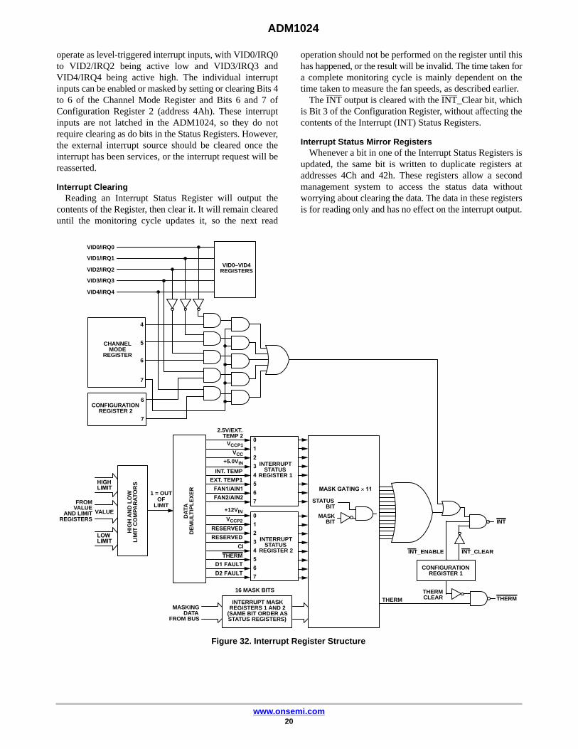
The ADM1024 Interrupt StructureThe Interrupt Structure of the ADM1024 is shown in
Figure 32. As each measurement value is obtained andstored in the appropriate value register, the value and thelimits from the corresponding limit registers are fed to thehigh and low limit comparators. The result of eachcomparison (1 = out of limit, 0 = in limit) is routed to thecorresponding bit input of the Interrupt Status Registers viaa data demultiplexer and used to set that bit high or low asappropriate.
The Interrupt Mask Registers have bits corresponding toeach of the Interrupt Status Register Bits. Setting anInterrupt Mask Bit high forces the corresponding Status Bitoutput low, while setting an Interrupt Mask Bit low allowsthe corresponding Status Bit to be asserted. After masking,the status bits are all OR’d together to produce the INToutput, which will pull low if any unmasked status bit goeshigh, i.e., when any measured value goes out of limit. TheADM1024 also has a dedicated output for temperatureinterrupts only, the THERM input/output Pin 2. Thefunction of this is described later.
The INT output is enabled when Bit 1 of ConfigurationRegister 1 (INT_Enable) is high, and Bit 3 (INT_Clear) is low.The INT pin has an internal, 100 k pullup resistor.
VID/IRQ InputsThe processor voltage ID inputs VID0 to VID4 can be
reconfigured as interrupt inputs by setting Bit 7 of theChannel Mode Register (address 16h). In this mode they
ADM1024
www.onsemi.com20
operate as level-triggered interrupt inputs, with VID0/IRQ0to VID2/IRQ2 being active low and VID3/IRQ3 andVID4/IRQ4 being active high. The individual interruptinputs can be enabled or masked by setting or clearing Bits 4to 6 of the Channel Mode Register and Bits 6 and 7 ofConfiguration Register 2 (address 4Ah). These interruptinputs are not latched in the ADM1024, so they do notrequire clearing as do bits in the Status Registers. However,the external interrupt source should be cleared once theinterrupt has been services, or the interrupt request will bereasserted.
Interrupt ClearingReading an Interrupt Status Register will output the
contents of the Register, then clear it. It will remain cleareduntil the monitoring cycle updates it, so the next read
operation should not be performed on the register until thishas happened, or the result will be invalid. The time taken fora complete monitoring cycle is mainly dependent on thetime taken to measure the fan speeds, as described earlier.
The INT output is cleared with the INT_Clear bit, whichis Bit 3 of the Configuration Register, without affecting thecontents of the Interrupt (INT) Status Registers.
Interrupt Status Mirror RegistersWhenever a bit in one of the Interrupt Status Registers is
updated, the same bit is written to duplicate registers ataddresses 4Ch and 42h. These registers allow a secondmanagement system to access the status data withoutworrying about clearing the data. The data in these registersis for reading only and has no effect on the interrupt output.
Figure 32. Interrupt Register Structure
INT
16 MASK BITS
VALUE
4
5
6
7
VID4/IRQ4
6
7
THERM THERM
VID0–VID4REGISTERS
CHANNELMODE
REGISTER
CONFIGURATIONREGISTER 2
FROMVALUE
AND LIMITREGISTERS
HIGHLIMIT
1 = OUT
DA
TAD
EM
ULT
IPL
EX
ER
INT. TEMP
EXT. TEMP1
FAN1/AIN1
FAN2/AIN2
RESERVED
RESERVED
CI
D1 FAULT
D2 FAULT
2.5V/EXT.TEMP 2
VCCP1
VCC
+5.0VIN
+12VIN
VCCP2
MASKINGDATA
FROM BUS
INTERRUPT MASKREGISTERS 1 AND 2
(SAME BIT ORDER ASSTATUS REGISTERS)
MASK GATING 11
STATUSBIT
MASKBIT
INT_ENABLE INT_CLEAR
CONFIGURATIONREGISTER 1
THERMCLEAR
THERM
0
1
2
3
4
5
6
7
INTERRUPTSTATUS
REGISTER 2
0
1
2
3
4
5
6
7
INTERRUPTSTATUS
REGISTER 1
HIG
H A
ND
LO
WL
IMIT
CO
MPA
RA
TO
RS
LOWLIMIT
OFLIMIT
VID2/IRQ2
VID3/IRQ3
VID0/IRQ0
VID1/IRQ1

ADM1024
www.onsemi.com21
Temperature Interrupt ModesThe ADM1024 has two distinct methods of producing
interrupts for out−of−limit temperature measurements fromthe internal or external sensors. Temperature errors cangenerate an interrupt on the INT pin along with otherinterrupts, but there is also a separate THERM pin thatgenerates an interrupt only for temperature errors.
Operation of the INT output for temperature interrupts isillustrated in Figure 33 Assuming that the temperature startsoff within the programmed limits and that temperatureinterrupt sources are not masked, INT will go low if thetemperature measured by any of the internal or externalsensors exceeds the programmed high temperature limit forthat sensor, or the hardware limits in register 13h, 14h, 17h,or 18h.
Figure 33. Operation of INT for TemperatureInterrupts
TEMP
HIGH LIMIT
LOW LIMIT
INT
1
1
1
1
1
1
100C
90C
80C
70C
60C
50C
40C
ACPICONTROL METHODSCLEAR EVENT
1ACPI AND DEFAULT CONTROL METHODSADJUST TEMPERATURE LIMIT VALUES.
Once the interrupt has been cleared, it will not bereasserted even if the temperature remains above the highlimit(s). However, INT will be reasserted if:
The temperature falls below the low limit for the sensor;
or:The high limit(s) is/are reprogrammed to a new value, and
the temperature then rises above the new high limit on thenext monitoring cycle;
or:The THERM pin is pulled low externally, which sets Bit 5
of Interrupt Status Register 2;
or:An interrupt is generated by another source.Similarly, should the temperature measured by a sensor
start off within limits then fall below the low limit, INT willbe asserted. Once cleared, it will not be reasserted unless:The temperature rises above the high limit;
or:The low limit(s) is/are reprogrammed, and the temperature
then falls below the new low limit;
or:The THERM pin is pulled low externally, which sets Bit 5
of Interrupt Status Register 2;
or:
An interrupt is generated by another source.
THERM Input/OutputThe Thermal Management Input/Output (THERM) is a
logic input/output with an internal, 100 k pullup resistor,that provides a separate output for temperature interruptsonly. It is enabled by setting Bit 2 of Configuration Register 1.The THERM output has two operating modes that can beprogrammed by Bit 3 of Configuration Register 2 (address4Ah). With this bit set to the default value of 0, the THERMoutput operates in “Default” interrupt mode. With this bit setto 1, the THERM output operates in “ACPI” mode.
Thermal interrupts can still be generated at the INT outputwhile THERM is enabled, but if these are not required they canbe masked by writing a 1 to Bit 0 of Configuration Register 2(address 4Ah). The THERM pin can also function as a logicinput for an external sensor, for example, a temperature sensorsuch as the ADM22105 used in Figure 35. If THERM is takenlow by an external source, the analog output will be forced toFFh to switch a controlled fan to maximum speed. This alsogenerates an INT output as previously described.
Default ModeIn Default mode, the THERM output operates like a
thermostat with hysteresis. THERM will go low and Bit 5 ofInterrupt Status Register 2 will be set, if the temperaturemeasured by any of the sensors exceeds the high limitprogrammed for that sensor. It will remain asserted untilreset by reading Interrupt Status Register 2, by setting Bit 6of Configuration Register 1, or when the temperature fallsbelow the low limit programmed for that sensor.
Figure 34. INT or THERM Output in Default Mode
TEMP
TEMPHIGH LIMIT
TEMPLOW LIMIT
THERM
CLEARED BYREAD OR
THERM CLEARPROGRAMMED
VALUEANALOGOUTPUT
CLEARED BYTEMP FALLINGBELOW LOW
LIMIT 0xFF
EXTTHERMINPUT
If THERM is cleared by reading the status register, it willbe reasserted after the next temperature reading andcomparison if it remains above the high limit.
If THERM is cleared by setting Bit 6 of ConfigurationRegister 1, it cannot be reasserted until this bit is cleared.
THERM will also be asserted if one of the hardwaretemperature limits at addresses 13h, 14h, 17h, or 18h isexceeded for three consecutive measurements. When thishappens, the analog output will be forced to FFh to boost acontrolled cooling fan to full speed.
Reading Status Register 1 will not clear THERM in thiscase, because errors caused by exceeding the hardware

ADM1024
www.onsemi.com22
temperature limits are stored in a separate register that is notcleared by reading the status register. In this case, THERMcan only be cleared by setting Bit 0 of ConfigurationRegister 2.
THERM will be cleared automatically if the temperaturefalls at least 5 degrees below the limit for three consecutivemeasurements.
ACPI ModeIn ACPI mode, THERM responds only to the hardware
temperature limits at addresses 13h, 14h, 17h, and 18h, notto the software-programmed limits.
Figure 35. THERM Output in ACPI Mode
TEMP
HARDWARETRIP POINT
THERM
ANALOGOUTPUT
PROGRAMMEDVALUE
5
0xFF 0xFFTHERMEXT
INPUT
THERM will go low if either the internal or externalhardware temperature limit is exceeded for threeconsecutive measurements. It will remain low until thetemperature falls at least 5 degrees below the limit for threeconsecutive measurements. While THERM is low, theanalog output will go to FFh to boost a controlled fan to fullspeed.
RESET Input/OutputRESET (Pin 12) is an I/O pin that can function as an
open-drain output, providing a low going 20 ms output pulsewhen Bit 4 of the Configuration Register is set to 1, providedthe reset function has first been enabled by setting Bit 7 ofInterrupt Mask Registers 2 to 1. The bit is automaticallycleared when the reset pulse is output. Pin 11 can also functionas a RESET input by pulling this pin low to reset the internalregisters of the ADM1024 to default values. Only thoseregisters that have power-on default values as listed inTable 10 are affected by this function. The DAC, Value, andLimit Registers are not affected.
NAND Tree TestsA NAND gate is provided in the ADM1024 for
Automated Test Equipment (ATE) board level connectivitytesting. The device is placed into NAND Test Mode bypowering up with Pin 11 held high. This pin is automaticallysampled after powerup; if it is connected high, then theNAND test mode is invoked.
In NAND test mode, all digital inputs may be tested asillustrated below. NTEST_OUT/ADD will become theNAND test output pin. To perform a NAND tree test, all pinsincluded in the NAND tree should first be driven high. Each
pin can then be toggled and a resulting toggle can beobserved on NTEST_OUT/ADD.
Allow for a typical propagation delay of 500 ns. Thestructure of the NAND tree is shown in Figure 36.
Figure 36. NAND Tree
LATCH
CQD
ENABLE
SDASCL
VID4
POWER−ONRESET
NTEST_IN/AOUT
NTEST_OUT/ADDVID0VID1VID2VID3
FAN1FAN2
Note that NTEST_OUT/ADD is a dual function line andif both functions are required, then this line should not behardwired directly to VCC/GND. Instead it should beconnected via a 5 k resistor.
Note: If any of the inputs shown in Figure 36 are unused,they should not be connected directly to ground, but via aresistor such as 10 k. This will allow the Automatic TestEquipment (ATE) to drive every input high so that the NANDtree test can be carried out properly.
Using the ADM1024
Power-on ResetWhen power is first applied, the ADM1024 performs a
power-on reset on several of its registers. Registers whosepower-on values are not shown have power-on conditionsthat are indeterminate (this includes the Value and LimitRegisters). The ADC is inactive. In most applications, usuallythe first action after power-on would be to write limits into theLimit Registers. Power-on reset clears or initializes thefollowing registers (the initialized values are shown inTable 12):• Configuration Registers 1 and 2
• Channel Mode Register
• Interrupt (INT) Status Registers 1 and 2
• Interrupt (INT) Status Mirror Registers 1 and 2
• Interrupt (INT) Mask Registers 1 and 2
• VID/Fan Divisor Register
• VID4 Register
• Chassis Intrusion Clear Register
• Test Register
• Analog Output Register
• Hardware Trip Registers
InitializationConfiguration Register initialization performs a similar,
but not identical, function to power-on reset. The TestRegister and Analog Output Register are not initialized.

ADM1024
www.onsemi.com23
Configuration Register initialization is accomplished bysetting Bit 7 of the Configuration Register high. This bitautomatically clears after being set.
Using the Configuration RegistersControl of the ADM1024 is provided through two
configuration registers. The ADC is stopped upon powerup,and the INT_Clear signal is asserted, clearing the INT output.The Configuration Registers are used to start and stop theADM1024; enable or disable interrupt outputs and modes,and provide the initialization function described above.
Bit 0 of Configuration Register 1 controls the monitoringloop of the ADM1024. Setting Bit 0 low stops themonitoring loop and puts the ADM1024 into a low powermode thereby reducing power consumption. Serial buscommunication is still possible with any register in theADM1024 while in low power mode. Setting Bit 0 highstarts the monitoring loop.
Bit 1 of Configuration Register 1 enables or disables theINT Interrupt output. Setting Bit 1 high enables the INToutput; setting Bit 1 low disables the output.
Bit 2 of Configuration Register 1 enables or disables theTHERM output. Setting Bit 1 high enables the INT output;setting Bit 1 low disables the output.
Bit 3 of Configuration Register 1 is used to clear the INTinterrupt output when set high. The ADM1024 monitoringfunction will stop until Bit 3 is set low. Interrupt Statusregister contents will not be affected.
Bit 4 of Configuration Register 1 causes a low going 45 ms(typ) pulse at the RESET pin (Pin 12).
Bit 6 of Configuration Register 1 is used to clear aninterrupt at the THERM output when it is set to 1.
Bit 7 of Configuration Register 1 is used to start aConfiguration Register Initialization when it is set to 1.
Bit 0 of Configuration Register 2 is used to masktemperature interrupts at the INT output when it is set to 1.The THERM output is unaffected by this bit.
Bits 1 and 2 of Configuration Register 2 lock the valuesstored in the Local and Remote Fan Control Registers ataddresses 13h and 14h. The values in these registers cannotbe changed until a power-on reset is performed.
Bit 3 of Configuration Register 2 selects the THERMinterrupt mode. The default value of 0 selects one−timemode. Setting this bit to 1 selects ACPI mode.
Starting ConversionThe monitoring function (analog inputs, temperature, and
fan speeds) in the ADM1024 is started by writing toConfiguration Register 1 and setting Start (Bit 0) high. TheINT_Enable (Bit 1) should be set to 1, and INT Clear (Bit 3)set to 0 to enable interrupts. The THERMenable bit (Bit 2)should be set to 1 and the THERM Clear bit (Bit 6) shouldbe set to 0 to enable temperature interrupts at the THERMpin. Apart from initially starting together, the analogmeasurements and fan speed measurements proceedindependently, and are not synchronized in any way.
The time taken to complete the analog measurementsdepends on how they are configured, as describedelsewhere. The time taken to complete the fan speedmeasurements depends on the fan speed and the number oftachometer output pulses per revolution.
Once the measurements have been completed, the resultscan be read from the Value Registers at any time.
Reduced Power and Shutdown ModeThe ADM1024 can be placed in a low power mode by
setting Bit 0 of the Configuration Register to 0. This disablesthe internal ADC. Full shutdown mode may then beachieved by setting Bit 0 of the Test Register to 1. This turnsoff the analog output and stops the monitoring cycle, ifrunning, but does not affect the condition of any of theregisters. The device will return to its previous state whenthis bit is reset to 0.
Application CircuitFigure 37 shows a generic application circuit using the
ADM1024. The analog monitoring inputs are connected tothe power supplies including two processor core voltageinputs. The VID inputs are connected to the processorvoltage ID pins. There are two tachometer inputs from fans,and the analog output is used to control the speed of a thirdfan. An opto-sensor for chassis intrusion detection isconnected to the CI input. Of course, in an actualapplication, every input and output may not be used, inwhich case unused analog and digital inputs should be tiedto analog or digital ground as appropriate.

ADM1024
www.onsemi.com24
Figure 37. Application Circuit
ADM1024
+5.0 V
SCL
SDA
SERIAL BUS
VID0/IRQ0
VID1/IRQ1
VID2/IRQ2
VID3/IRQ3
VID4/IRQ4
D1+
12 V
5.0 V
5.0 V
FAN1/AIN1
FAN2/AIN2
CI
GND D
74HC132MRD901
1N9145.0 V
1N914
N1
N2
N3
N4
CMOSBACKUP
BATTERY1
2
3
4
5
6
7
14
13
12
11
10
9
8 12 V
2N2219A
OP295 NTEST_IN/AOUT
THERM
THERM I/O TOOTHER CIRCUITS
NTEST_OUT/ADD 1
2
3
4
5
6
7
8
9
10
11
12
24
23
22
21
20
19
18
17
16
15
14
13
0.1F10FVCC
VCC
RESET
INT INT TO PROCESSOR
D1–
+VCCP1
+2.5VIN/D2+
+VCCP2/D2–
+5.0VIN
+12VIN
TRANSISTORSENSINGTEMP.
PROCESSORPINS OFFROM VID
510k
510k
510k
510k
510k
100k
470k
10k
10k
10k
39k

ADM1024
www.onsemi.com25
ADM REGISTERS
Table 10. ADDRESS POINTER REGISTER
Bit Name R/W Description
7–0 Address Pointer W Address of ADM1024 registers. See the following tables for details.
Table 11. LIST OF REGISTERS
HexAddr Description
Power-on Value(Binary Bit 7−0) Notes
13h Internal TemperatureHardware Trip Point
= 70°C Can be written only if the write once bit in Configuration Register 2has not been set. Values higher than 70°C will have no affect as thefixed trip point in register 16h will be reached first.
14h External TemperatureHardware Trip Point
= 85°C Can be written only if the write once bit in Configuration Register 2has not been set. Values higher than 85°C will have no affect as thefixed trip point in register 17h will be reached first.
15h Test Register 0000 00X0 Setting Bit 0 of this register to 1 selects shutdown mode. Caution: Donot write to any other bits in this register.
16h Channel Mode Register 0000 0000 This register configures the input channels and configures VID0 toVID4 as processor voltage ID or interrupt inputs.
17h Internal TemperatureFixed Hardware Trip Point
= 70°C Read Only. Cannot be changed.
18h External TemperatureFixed Hardware Trip Point
= 85°C Read Only. Cannot be changed.
19h Programmed Value of AnalogOutput
1111 1111
1Ah AIN1 Low Limit Indeterminate
1Bh AIN2 Low Limit Indeterminate
20h 2.5 V Measured Value/Ext. Temp2 Indeterminate Read Only
21h VCCP1 Measured Value Indeterminate Read Only
22h VCC Measured Value Indeterminate Read Only
23h 5.0 V Value Indeterminate Read Only
24h 12 V Measured Value Indeterminate Read Only
25h VCCP2 Measured Value Indeterminate Read Only
26h Ext. Temp1 Value Indeterminate Read Only. Stores the measurement from a diode sensor connectedto Pins 13 and 14.
27h Internal Temperature Value Indeterminate Read Only. This register is used to store eight bits of the internaltemperature reading.
28h FAN1/AIN1 Value Indeterminate Read Only. Stores FAN1 or AIN1 reading, depending on theconfiguration of Pin 5.
29h FAN2/AIN1 Value Indeterminate Read Only. Stores FAN2 or AIN2 reading, depending on theconfiguration of Pin 6.
2Ah Reserved Indeterminate
2Bh 2.5 V/Ext. Temp2 High Limit Indeterminate Stores high limit for 2.5 V input or, in temperature mode, this registerstores the high limit for a diode sensor connected toPins 17 and 18.
2Ch 2.5 V/Ext. Temp2 Low Limit Indeterminate Stores low limit for 2.5 V input or, in temperature mode, this registerstores the low limit for a diode sensor connected toPins 17 and 18.
2Dh VCCP1 High Limit Indeterminate
2Eh VCCP1 Low Limit Indeterminate
2Fh VCC High Limit Indeterminate
30h VCC Low Limit Indeterminate
31h 5.0 V High Limit Indeterminate
32h 5.0 V Low Limit Indeterminate
33h 12 V High Limit Indeterminate

ADM1024
www.onsemi.com26
Table 11. LIST OF REGISTERS
HexAddr Notes
Power-on Value(Binary Bit 7−0)Description
34h 12 V Low Limit Indeterminate
35h VCCP2 High Limit Indeterminate
36h VCCP2 Low Limit Indeterminate
37h Ext. Temp1 High Limit Indeterminate Stores high limit for a diode sensor connected to Pins 13 and 14.
38h Ext. Temp1 Low Limit Indeterminate Stores low limit for a diode sensor connected to Pins 13 and 14.
39h Internal Temp. High Limit Indeterminate Stores the high limit for the internal temperature reading.
3Ah Internal Temp. Low Limit Indeterminate Stores the low limit for the internal temperature reading.
3Bh AIN1/FAN1 High Limit Indeterminate Stores high limit for AIN1 or FAN1, depending on the configuration ofPin 5.
3Ch AIN2/FAN2 High Limit Indeterminate Stores high limit for AIN2 or FAN2, depending on the configuration ofPin 6.
3Dh Reserved Indeterminate
3Eh Company ID Number 0100 0001 This location will contain the company identification number (ReadOnly).
3Fh Revision Number 0001 nnnn Last four bits of this location will contain the revision number of thepart (Read Only).
40h Configuration Register 1 0000 1000 See Table 10
41h Interrupt INT Status Register 1 0000 0000 See Table 11
42h Interrupt INT Status Register 2 0000 0000 See Table 12
43h INT Mask Register 1 0000 0000 See Table 13
44h INT Mask Register 2 0000 0000 See Table 14
46h Chassis Intrusion Clear Register 0000 0000 See Table 15
47h VID0–3/Fan Divisor Register 0101 (VID3–VID0) See Table 16
49h VID4 Register 1000 000 (VID4) See Table 17
4Ah Configuration Register 2 0000 0000 See Table 18
4Ch Interrupt Status Register Mirror 1 0000 0000 See Table 19
4Dh Interrupt Status Register Mirror 2 0000 0000 See Table 20
Table 12. REGISTER 16H, CHANNEL MODE REGISTER (POWER-ON DEFAULT, 00H)
Bit Name R/W Description
0 FAN1/AIN1 R/W Clearing this bit to 0 configures Pin 5 as FAN1 input. Setting this bit to 1 configuresPin 5 as AIN1. Power−on default = 0.
1 FAN2/AIN2 R/W Clearing this bit to 0 configures Pin 6 as FAN2 input. Setting this bit to 1 configuresPin 6 as AIN2. Power−on default = 0.
2 2.5 V, VCCP2/D2 R/W Clearing this bit to 0 configures Pins 17 and 18 to measure VCCP2 and 2.5 V. Settingthis bit to 1 configures Pins 17 and 18 as an input for a second remotetemperature−sensing diode. Power−on default = 0.
3 Int. VCC R/W Clearing this bit to 0 sets the measurement range for the internal VCC measurementto 3.3 V. Setting this bit to 1 sets the internal VCC measurement range to 5.0 V.Power−on default = 0.
4 IRQ0 EN R/W Setting this bit to 1 enables Pin 24 as an active high interrupt input, provided Pins 20to 24 have been configured as interrupts by setting Bit 7 of the Channel ModeRegister. Power−on default = 0.
5 IRQ1 EN R/W Setting this bit to 1 enables Pin 23 as an active high interrupt input, provided Pins 20to 24 have been configured as interrupts by setting Bit 7 of the Channel ModeRegister. Power−on default = 0.
6 IRQ2 EN R/W Setting this bit to 1 enables Pin 22 as an active high interrupt input, provided Pins 20to 24 have been configured as interrupts by setting Bit 7 of the Channel ModeRegister. Power−on default = 0.
7 VID/IRQ R/W Clearing this bit to 0 configures Pins 20 to 24 as processor voltage ID inputs. Settingthis bit to 1 configures Pins 20 to 24 as interrupt inputs. Power−on default = 0.

ADM1024
www.onsemi.com27
Table 13. REGISTER 40H, CONFIGURATION REGISTER 1 (POWER-ON DEFAULT, 08H)
Bit Name R/W Description
0 START R/W Logic 1 enables startup of ADM1024; Logic 0 places it in standby mode. Caution:The outputs of the interrupt pins will not be cleared if the user writes a 0 to thislocation after an interrupt has occurred (see “INT Clear” bit). At startup, limitchecking functions and scanning begins. Note, all high and low limits should be setinto the ADM1024 prior to turning on this bit (Power−On Default = 0).
1 INT_Enable R/W Logic 1 enables the INT_output. 1 = Enabled 0 = Disabled (Power−On Default = 0).
2 THERMEnable
R/W 0 = THERM disabled1 = THERM enabled
3 INT_Clear R/W During Interrupt Service Routine (ISR), this bit is asserted Logic 1 to clear INT outputwithout affecting the contents of the Interrupt Status Register. The device will stopmonitoring. It will resume upon clearing of this bit. (Power−On Default = 0)
4 RESET R/W Setting this bit generates a low going 45 ms reset pulse at Pin 12. This bit isself−clearing and power−on default is 0.
5 Reserved R/W Default = 0
6 THERM CLR R/W A 1 clears the THERM output without changing the Status Register contents.
7 Initialization R/W Logic 1 restores power−on default values to the Configuration Register, InterruptStatus Registers, Interrupt Mask Registers, Fan Divisor Register, and theTemperature Configuration Register. This bit automatically clears itself since thepower−on default is 0.
Table 14. REGISTER 41H, INTERRUPT STATUS REGISTER 1 (POWER-ON DEFAULT, 00H)
Bit Name R/W Description
0 2.5 V/External Temp2Error
Read only A 1 indicates that a High or Low limit has been exceeded.
1 VCCP1 Error Read only A 1 indicates that a High or Low limit has been exceeded.
2 VCC Error Read only A 1 indicates that a High or Low limit has been exceeded.
3 5.0 V Error Read only A 1 indicates that a High or Low limit has been exceeded.
4 Internal Temp Error Read only A 1 indicates that a temperature interrupt has been set, or that a High or Low limithas been exceeded.
5 External Temp1 Error Read only A 1 indicates that a temperature interrupt has been set, or that a High or Low limithas been exceeded.
6 FAN1/AIN1 Error Read only A 1 indicates that a High or Low limit has been exceeded.
7 FAN2/AIN2 Error Read only A 1 indicates that a High or Low limit has been exceeded.
Table 15. REGISTER 42H, INTERRUPT STATUS REGISTER 2 (POWER-ON DEFAULT, 00H) (Note 1 and 2)
Bit Name R/W Description
0 12 V Error Read only A 1 indicates a High or Low limit has been exceeded.
1 VCCP2 Error Read only A 1 indicates a High or Low limit has been exceeded.
2 Reserved Read only Undefined.
3 Reserved Read only Undefined.
4 Chassis Error Read only A 1 indicates Chassis Intrusion has gone high.
5 THERM Interrupt Read only Indicates that THERM pin has been pulled low by an external source.
6 D1 Fault Read only Short or Open−Circuit Sensor Diode D1.
7 D2 Fault Read only Short or Open−Circuit Sensor Diode D2.
1. Any time the Status Register is read out, the conditions (i.e., Register) that are read are automatically reset. In the case of the channel priorityindication, if two or more channels were out of limits, then another indication would automatically be generated if it was not handled duringthe ISR.
2. In the Mask Register, the errant voltage interrupt may be disabled until the operator has time to clear the errant condition or set the limithigher/lower.

ADM1024
www.onsemi.com28
Table 16. REGISTER 43H, INT INTERRUPT MASK REGISTER 1 (POWER-ON DEFAULT, 00H)
Bit Name R/W Description
0 2.5 V/Ext. Temp2 R/W A 1 disables the corresponding interrupt status bit for INT interrupt.
1 VCCP1 R/W A 1 disables the corresponding interrupt status bit for INT interrupt.
2 VCC R/W A 1 disables the corresponding interrupt status bit for INT interrupt.
3 5.0 V R/W A 1 disables the corresponding interrupt status bit for INT interrupt.
4 Int. Temp R/W A 1 disables the corresponding interrupt status bit for INT interrupt.
5 Ext. Temp1 R/W A 1 disables the corresponding interrupt status bit for INT interrupt.
6 FAN1/AIN1 R/W A 1 disables the corresponding interrupt status bit for INT interrupt.
7 FAN2/AIN2 R/W A 1 disables the corresponding interrupt status bit for INT interrupt.
Table 17. REGISTER 44H, INT INTERRUPT MASK REGISTER 2 (POWER-ON DEFAULT, 00H)
Bit Name R/W Description
0 12 V R/W A 1 disables the corresponding interrupt status bit for INT interrupt.
1 VCCP2 R/W A 1 disables the corresponding interrupt status bit for INT interrupt.
2 Reserved R/W Powerup Default Set to Low.
3 Reserved R/W Powerup Default Set to Low.
4 CI R/W A 1 disables the corresponding interrupt status bit for INT interrupt.
5 THERM (Input) R/W A 1 disables the corresponding interrupt status bit for INT interrupt.
6 D1 Fault R/W A 1 disables the corresponding interrupt status bit for INT interrupt.
7 D2 Fault R/W A 1 disables the corresponding interrupt status bit for INT interrupt.
Table 18. REGISTER 46H, CHASSIS INTRUSION CLEAR (POWER-ON DEFAULT, 00H)
Bit Name R/W Description
0–6 Reserved Read only Undefined, always reads as 00h.
7 Chassis Int. Clear R/W A 1 outputs a minimum 20 ms active low pulse on the Chassis Intrusion pin. Theregister bit clears itself after the pulse has been output.
Table 19. REGISTER 47H, VID0−3/FAN DIVISOR REGISTER (POWER-ON DEFAULT, 0101(VID3−0))
Bit Name R/W Description
0–3 VID Read only The VID<3:0> inputs from processor core power supplies to indicate the operatingvoltage (e.g., 1.3 V to 3.5 V).
4–5 FAN1 Divisor R/W Sets counter prescaler for FAN1 speed measurement. <5:4> = 00 – divide by 1<5:4> = 01 – divide by 2<5:4> = 10 – divide by 4<5:4> = 11 – divide by 8
6–7 FAN2 Divisor R/W Sets counter prescaler for FAN2 speed measurement. <7:6> = 00 – divide by 1<7:6> = 01 – divide by 2<7:6> = 10 – divide by 4<7:6> = 11 – divide by 8
Table 20. REGISTER 49H, VID4/DEVICE ID REGISTER (POWER-ON DEFAULT, 1000000(VID4))
Bit Name R/W Description
0 VID4 Read only VID4 Input from Pentium
1–7 Reserved Read only Undefined, always reads as 1000 000(VID4)

ADM1024
www.onsemi.com29
Table 21. REGISTER 4AH, CONFIGURATION REGISTER 2 (POWER-ON DEFAULT, [7:0] = 0X00H)
Bit Name R/W Description
0 Thermal INT Mask R/W Setting this bit masks the thermal interrupts for the INT output ONLY. The THERMoutput will still be generated, regardless of the setting of this bit.
1 Ambient Temp FanControl Register Write
Once Bit
R/W once Writing a 1 to this bit will lock in the values set into the ambient temperatureautomatic fan control register 13h. This register will not be able to be written againuntil a reset is performed (either POR, Hard Reset, or Soft Reset).
2 Remote Temp FanControl Register Write
Once Bit
R/W once Writing a 1 to this bit will lock in the values set into the remote temperature automaticfan control register 14h. This register will not be able to be written again until a resetis performed (either POR, Hard Reset, or Soft Reset).
3 THERM R/W If this bit is 0, the THERM output operates in default mode.
Interrupt Mode If this bit is 1, the THERM output operates in ACPI mode.
4, 5 Reserved Read only Reserved
6 IRQ3 EN R/W Setting this bit to 1 enables Pin 21 as an active high interrupt input, provided Pins 20to 24 have been configured as interrupts by setting Bit 7 of the Channel ModeRegister. Power−on default = 0.
7 IRQ4 EN R/W Setting this bit to 1 enables Pin 20 as an active high interrupt input, provided Pins 20to 24 have been configured as interrupts by setting Bit 7 of the Channel ModeRegister. Power−on default = 0.
Table 22. REGISTER 4CH, INTERRUPT STATUS REGISTER 1 MIRROR (POWER-ON DEFAULT, [7:0] = 00H)
Bit Name R/W Description
0 2.5 V/Ext. Temp2 Error Read only A 1 indicates that a High or Low limit has been exceeded.
1 VCCP1 Error Read only A 1 indicates that a High or Low limit has been exceeded.
2 VCC Error Read only A 1 indicates that a High or Low limit has been exceeded.
3 5.0 V Error Read only A 1 indicates that a High or Low limit has been exceeded.
4 Internal Temp Error Read only A 1 indicates that a temperature interrupt has been set, or that a High or Low limithas been exceeded.
5 External Temp1 Error Read only A 1 indicates that a temperature interrupt has been set, or that a High or Low limithas been exceeded.
6 FAN1/AIN1 Error Read only A 1 indicates that a High or Low limit has been exceeded.
7 FAN2/AIN2 Error Read only A 1 indicates that a High or Low limit has been exceeded.
Table 23. REGISTER 4DH, INTERRUPT STATUS REGISTER 2 MIRROR (POWER-ON DEFAULT, [7:0] = 00H) (Note 1)
Bit Name R/W Description
0 12 V Error Read only A 1 indicates a High or Low limit has been exceeded.
1 VCCP2 Error Read only A 1 indicates a High or Low limit has been exceeded.
2 Reserved Read only Undefined.
3 Reserved Read only Undefined.
4 Chassis Error Read only A 1 indicates Chassis Intrusion has gone high.
5 THERM Interrupt Read only Indicates that THERM pin has been pulled low by an external source.
6 D1 Fault Read only Short or Open−Circuit Sensor Diode D1.
7 D2 Fault Read only Short or Open−Circuit Sensor Diode D2.
1. An error that causes continuous interrupts to be generated may be masked in its respective mask register, until the error can be alleviated.
Table 24. ORDERING INFORMATION
Device Order Number Temperature Range Package Type Shipping†
ADM1024ARUZ−REEL 0°C to +100°C 24-Lead TSSOP 2,500 Tape & Reel
†For information on tape and reel specifications, including part orientation and tape sizes, please refer to our Tape and Reel PackagingSpecifications Brochure, BRD8011/D.
*The “Z’’ suffix indicates Pb-Free part.

ADM1024
www.onsemi.com30
PACKAGE DIMENSIONS
TSSOP24 7.8x4.4, 0.65PCASE 948H
ISSUE B
DIM
D
MIN MAX
7.90
MILLIMETERS
E1 4.30 4.50
A 1.20A1 0.05 0.15
L 0.50 0.75e 0.65 BSC
c 0.09 0.20b 0.19 0.30
L2 0.25 BSCM 0 8
NOTES:1. DIMENSIONING AND TOLERANCING PER ASME Y14.5M, 1994.2. CONTROLLING DIMENSION: MILLIMETERS.3. DIMENSION b DOES NOT INCLUDE DAMBAR PROTRUSION.
DAMBAR PROTRUSION SHALL BE 0.08 MAX AT MMC. DAMBARCANNOT BE LOCATED ON THE LOWER RADIUS OF THE FOOT.
4. DIMENSION D DOES NOT INCLUDE MOLD FLASH,PROTRUSIONS OR GATE BURRS. MOLD FLASH,PROTRUSIONS OR GATE BURRS SHALL NOT EXCEED 0.15PER SIDE. DIMENSION D IS DETERMINED AT DATUM PLANE H.
5. DIMENSION E1 DOES NOT INCLUDE INTERLEAD FLASH ORPROTRUSION. INTERLEAD FLASH OR PROTRUSION SHALLNOT EXCEED 0.25 PER SIDE. DIMENSION E1 IS DETERMINEDAT DATUM PLANE H.
6. DATUMS A AND B ARE DETERMINED AT DATUM PLANE H.7. A1 IS DEFINED AS THE VERTICAL DISTANCE FROM THE SEAT-
ING PLANE TO THE LOWEST POINT ON THE PACKAGE BODY.
7.70
---
24X1.15
24X 0.42
0.65DIMENSIONS: MILLIMETERS
PITCH
SOLDERING FOOTPRINT
E 6.40 BSC
6.70
RECOMMENDED
L
L2
GAUGE
DETAIL A
PLANE
C
DETAIL A
MEND VIEWc
H
0.10SEATINGPLANESIDE VIEW
A
C
0.05 C
C24X
A1
PIN 1REFERENCE
D
E1
24X be
BM0.10 AC
TOP VIEW
B0.15 C1 12
1324
A
B
NOTE 3
2X 12 TIPS
E
NOTE 6NOTE 6
NOTE 4
NOTE 5
S S
S
ON Semiconductor and the are registered trademarks of Semiconductor Components Industries, LLC (SCILLC) or its subsidiaries in the United States and/or other countries.SCILLC owns the rights to a number of patents, trademarks, copyrights, trade secrets, and other intellectual property. A listing of SCILLC’s product/patent coverage may be accessedat www.onsemi.com/site/pdf/Patent−Marking.pdf. SCILLC reserves the right to make changes without further notice to any products herein. SCILLC makes no warranty, representationor guarantee regarding the suitability of its products for any particular purpose, nor does SCILLC assume any liability arising out of the application or use of any product or circuit, andspecifically disclaims any and all liability, including without limitation special, consequential or incidental damages. “Typical” parameters which may be provided in SCILLC data sheetsand/or specifications can and do vary in different applications and actual performance may vary over time. All operating parameters, including “Typicals” must be validated for eachcustomer application by customer’s technical experts. SCILLC does not convey any license under its patent rights nor the rights of others. SCILLC products are not designed, intended,or authorized for use as components in systems intended for surgical implant into the body, or other applications intended to support or sustain life, or for any other application in whichthe failure of the SCILLC product could create a situation where personal injury or death may occur. Should Buyer purchase or use SCILLC products for any such unintended orunauthorized application, Buyer shall indemnify and hold SCILLC and its officers, employees, subsidiaries, affiliates, and distributors harmless against all claims, costs, damages, andexpenses, and reasonable attorney fees arising out of, directly or indirectly, any claim of personal injury or death associated with such unintended or unauthorized use, even if such claimalleges that SCILLC was negligent regarding the design or manufacture of the part. SCILLC is an Equal Opportunity/Affirmative Action Employer. This literature is subject to all applicablecopyright laws and is not for resale in any manner.
PUBLICATION ORDERING INFORMATIONN. American Technical Support: 800−282−9855 Toll FreeUSA/Canada
Europe, Middle East and Africa Technical Support:Phone: 421 33 790 2910
Japan Customer Focus CenterPhone: 81−3−5817−1050
ADM1024/D
LITERATURE FULFILLMENT:Literature Distribution Center for ON Semiconductor19521 E. 32nd Pkwy, Aurora, Colorado 80011 USAPhone: 303−675−2175 or 800−344−3860 Toll Free USA/CanadaFax: 303−675−2176 or 800−344−3867 Toll Free USA/CanadaEmail: [email protected]
ON Semiconductor Website: www.onsemi.com
Order Literature: http://www.onsemi.com/orderlit
For additional information, please contact your localSales Representative