
Addressing 7nm Arm® DynamIQ™ cluster design … · Early access to new Arm IP during RTL...
31
© 2017 Arm Limited Addressing 7nm Arm® DynamIQ™ Cluster Design Challenges Using the Cadence® Digital Implementation Flow Shawn Hung Sr. Engineering Manager, Arm Jerry Chen Sr. AE Manager, Cadence Arm Tech Symposia 2017, Taipei
Transcript of Addressing 7nm Arm® DynamIQ™ cluster design … · Early access to new Arm IP during RTL...

© 2017 Arm Limited
Addressing 7nm Arm® DynamIQ™ Cluster Design
Challenges Using the Cadence® Digital
Implementation Flow
Shawn Hung Sr. Engineering Manager, Arm
Jerry Chen Sr. AE Manager, Cadence
Arm Tech Symposia 2017, Taipei

© 2017 Arm Limited 2
Agenda
Arm DynamIQ introduction
Arm-Cadence collaboration
Cadence flow for 7nm DynamIQ Shared Unit (DSU) implementation
7nm DSU implementation best practices
• Floor-planning
• Placement
• Clock choices
• Handling crosstalk
• Signoff ECO for power/timing
Wrap-up followed by Q&A

© 2017 Arm Limited
Arm DynamIQIntroduction

© 2017 Arm Limited 4
Arm DynamIQ design – Multi-core redefined
New single cluster design
Greater flexibility, with or without big.LITTLE™ technology
Redesigned memory subsystem
Advanced compute capabilities

© 2017 Arm Limited 5
Arm Cortex-A75: New premium performance pointCortex®-A75
Massive uplift for laptop-ready performance
Smartphone power profile
AI for edge to cloud compute
Massive uplift for laptop-ready performance
Smartphone power profile
AI for edge to cloud compute
Estimated device performance using SPECINT2006, final device results may vary Comparison using Cortex-A73 at 2.4GHz vs Cortex-A75 at 3GHz
>50%more performance
compared to current devices

© 2017 Arm Limited 6
2.5xhigher power efficiency
compared to current devices
Cortex-A55: Efficient performance redefined Cortex-A55
Breakthrough power efficiency
Higher sustained performance
More intelligent compute at the edge
Comparison using Cortex-A53 in 28nm devices vs Cortex-A55 in 16nm devices
© 2017 Arm Limited 7
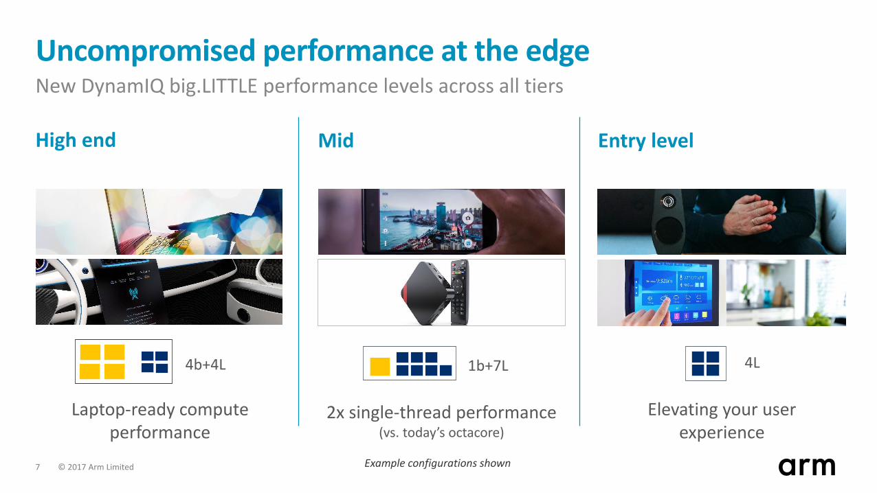
Uncompromised performance at the edgeNew DynamIQ big.LITTLE performance levels across all tiers
High end Mid Entry level
4L1b+7L
Example configurations shown
4b+4L
Laptop-ready compute performance
2x single-thread performance(vs. today’s octacore)
Elevating your user experience

© 2017 Arm Limited
Arm-Cadence Collaboration

© 2017 Arm Limited 9
Arm and Cadence project collaboration
Arm and Cadence are successfully engaged in several joint projects
20122011 20132010 2014 2015
iRM
Implementation Reference
Methodology
Testchip
Hardened Macro Mali T678
iRM
Samsung 20nm
testchip
Cortex-A15iRM
cmos32lp
TSMC 28hpm
Cortex-A57 iRM
cmos32lp
Cortex-A7 iRM
TSMC 28hpm
IBM 20nm
testchip
TSMC 20nm Cortex-A15
testchip
SeahawkQuad-A15
GPU Mali-T604
iRMTSMC 28hpm
Cortex-A7 iRM
Samsung 20nm
testchip
TSMC 40lp POP IP
Dual-A9
TSMC 28hpm
Cortex-A12 iRM
Cortex-A9Hard macro
IBM Arm 14nm FinFET
testchip
TSMC 16FF Cortex-A57
Cortex-A53 iRM
Cortex-A53
Next-gen Mali Cortex
-A57
TSMC 28hpm
TSMC 28hpm
tsmc28hpm
Samsung A7 14nm FINFET
Armv8 Arm big.LITTLE™ +
GPU Testchip
Seahawk 2Dual-A15
TSMC 28hpm
Cortex-A15 R3 iRMUpdate
TSMC 28hpm Cortex-A15
LP iRM
TSMC 16FF Cortex-
A53/A57
GF 28nm A12
CCN-504 iRM
Cortex-M7 iRM
Next-gen System IP
iRM
Cortex-A57 iRM
refresh
GF28nm A17
CCN-504 iRM TSMC
28hpm
Cortex-A17 iRM
Mali T720 iRM
TSMC28hpm
Cortex-A72 iRM
TSMC 16FF+
TSMC 40LP
Mail-T880
CortexA53
T860 GPU
Cortex-A72 CPU
Armv8 Arm big.LITTLE +
GPU Testchip
TSMC 16FF+
N10 Cortex-A73
TSMC 16FF Cortex-A53/A57
PPPA Push
TSMC 16FF+
2016
TSMC 16FFC
TSMC 16FF+
2 MP1 A73 TSMC 16FFC
High Performance
Low Power
Cortex-A73 RAK
Mali-G71 RAK
Cortex-A35RAK
Cortex-A75 RAK
RAK
Cortex-R52RAK
Rapid Adoption Kit
Cortex-M23RAK
Cortex-M33RAK
Mali-G72 RAK
Cortex-A55 RAK
DSURAK
TSMC7nm

© 2017 Arm Limited 10
Arm and Cadence collaboration
Close collaboration with Arm IP and flow developers
Early access to new Arm IP during RTL development cycle enables better understanding of EDA requirements
Cadence tool and flow enhancements implemented in parallel with Arm IP
Cadence R&D
Tool & Flow
updates
Arm R&D
Arm IP Updates
Cadence®Digital Design tools
Investigations / experiments / tool
enhancementsInitialArm IPEarly collaboration ensures tool support in place

© 2017 Arm Limited 11
Cadence Implementation Flow
Place and Route Setup(Cadence Innovus™)
RTL synthesis to gates(Cadence Genus™)
Synthesis / Mapping
Scan Insertion/Compression
Multibit Insertion
LibrariesDEF/FloorplanUPFSDCLEF filesQRC tech Files
Design RTL
Netlist / ScanDEF
Floorplan InitializationMMMC SetupMultiBit Level Shifter Insertion
Placement
Timing-Aware PlacementScan ReorderingClock estimation (Early Clock Flow)PRECTS optimization
+ AdditionalConstraints
- Bounds- Blockages- Route Guides- NDR- CTS constraints
Clock Tree SynthesisCTS with Useful Skew EnabledClock Tree Routing
POSTCTS Setup OptPOSTCTS Hold Fixing
Signal Routing
Timing-aware Signal Routing
PostRoute Optimization
POSTROUTE Setup OptSkew OptimizationIncremental POSTROUTE OptPOSTROUTE Hold Fixing
LibrariesLEF files
SignoffExtraction
(QRC)Multi-corner RC extraction
STA(Cadence Tempus™)
- Multi corner - Multi mode- STA signoff settings
- Graph Based STA- Path based STA
on failing paths
RC SPEF
Netlist and DEF
SignoffConstraints(SDC)

© 2017 Arm Limited 12
Stylus Common User Interface
Arm DSU project used the Stylus Common User Interface
• Streamline synthesis to signoff flow
• Script consistency across the whole digital flow
• Simple reuse of code & fewer files to maintain
• Faster debug with robust common reporting
• Easy to capture advanced flow recipes such as 7nm
Enables each designer to be more productive
Common User Interface
Improved ease-of-use and designer productivity
Common UI
Uniform Commands
Across Tools
Automated Flow and Metrics
Uniform Reports and
Logs
Common Initialization Commands
Uniform Database Access
Uniform New GUI Across Tools

© 2017 Arm Limited
7nm DSU Implementation Flow

© 2017 Arm Limited 14
7nm process changes
On-chip variation requires more accuracy, SOCV
Trim metal shapes needed for best routing density
VIA pillars for high-performance designs
Significant RC differences across layer stack
Lower voltage needs accurate waveform for delay calculation
Wire1
TR
IM Wire2 Wire3
TR
IM
Der
ate
Path depth
Ideal derateOCV derateAOCV derateSOCV derate
> 30X interconnect
delaydifference
between layers
The output switch only at the tail of the input waveform
Vtn
Vtp
Vdd
Both transistors are off, Output floating
PMOS off NMOS on, Output switching
PMOS on NMOS off, Output no change

© 2017 Arm Limited 15
7nm Cadence flow
Routing
• Timing driven
• Aggressive wire spreading to control SI effects of long parallel wires
Signoff
• Complete 7nm timing signoff
• SOCV enabled
Signoff ECO
• Integrated into Implementation flow
• Path based to avoid pessimism
• Focus on total power reduction
Clock tree synthesis
• Non default rules for clock nets based on 7nm layer stack
• Cloning and merging of ICGs
Genus(Physical Synthesis)
Inn
ovu
s(I
mp
lem
enta
tio
n)
GigaPlace™
GigaOpt™
(pre-cts)
CCOpt™
(CTS)
NanoRoute™
GigaOpt(post-route)
Tempus(Signoff STA)
Quantus™
(Signoff Extr)
GDS
RTL
Co
nfo
rmal
®
(Fo
rmal
Eq
)
Synthesis
• Early Physical Synthesis considering 7nm rules
Placement
• No placement guides / regions
• Early clock flow
• No manual latencies for RAMs or ICGs

© 2017 Arm Limited 16
DSU MP8 configuration
RTL Configuration
4x Cortex-A75 + 4x Cortex-A55 MP8
2MB L3 cache
Asynchronous DVFS for cores
AMBA® ACE Bus Interface
Accelerator Coherency Port, Peripheral Port Interface
Cortex-A75 config: 64KB L1, 512KB L2, ECC/Paritypresent, Crypto
Cortex-A55 config: 32KB L1, 256KB L2, ECC/Parity present, Crypto, NEON
Target Frequency: 2.5 GHz @ TT/1.0V/85C*Zoomed-in view of DSU layout
Example configuration
4b+4L
4x Cortex-A75

© 2017 Arm Limited
7nm DSU Implementation Best Practices

© 2017 Arm Limited 18
Floorplanning DSU in the SoC context
In a typical SoC floorplan, the CPU cluster would occupy one corner of the die
Need to consider SoC floorplan along with DSU
Cores and DSU shaped to be efficient at the SoC level
Some examples for a 2x Cortex-A75 + 4x Cortex-A55 configuration shown here
*Schematics with representative scaling

© 2017 Arm Limited 19
Example rectilinear floor plan resultsFloorplan details
2x Cortex-A75 + 4x Cortex-A55
No notches along die edges
Ports accessible close to die center, with some flexibility to move
• Timing goals are met
• Exact same flow used for all floorplan trials
• No placement guides / additional tuning necessary*Zoomed-in view of DSU layout
Results

© 2017 Arm Limited 20
7nm DSU floor planning and placement considerations
Size the “core” channels to accommodate logic + routing
• Use density screens to limit the cell density in “core” channels
• For typical RAM channels, use soft blockages to ensure long wires are buffered optimally
• Logic module placement follows DSU data path flow
• Placement guides / regions not found to be necessary
SI and wire delay avoidance is critical in macro dominated floorplans, especially for 7nm
*Zoomed-in view of DSU layout
DSU logic module placement
RAM channels

© 2017 Arm Limited 21
Placement guides
Historically designers used placement guides to improving timing closure
• Time-consuming, iterative, manual process, which may not converge
• Needs to be manually recreated for each floorplan revision
Innovus Implementation System natively understands DSU data path flow
• No need for manual placement guides
• Generally user-defined placement guides make results worse

© 2017 Arm Limited 22
Clock latency planning
DSU design uses a number of levels of architectural clock gates for achieving low power
For optimal timing closure, pre-CTS clock gate latency estimations should be applied to the architectural clock gates
• Manual latency estimation can be error prone and iterative
• Innovus early clock flow fully automates the latency calculation significantly improving accuracy
• Enables faster floorplan trials and design closure
Early clock flow used for 7nm DSU implementation
Inn
ovu
s(I
mp
lem
enta
tio
n)
GigaPlace
GigaOpt(pre-cts)
CCOpt(CTS)
NanoRoute
GigaOpt(post-route)
GigaOpt
Optimization driven by accurate timing, improving QoRCCOpt
Clock tree synthesis implements latency
GigaPlace
Latencies automatically generated

© 2017 Arm Limited 23
SI avoidance during initial placement
Floorplan creates long thin channels between CPUs and DSU logic
Need to control cell density in these channels to reduce SI effects
Initial placement should consider SI timing effects
Std.cell snapshot in channel
Route segments

© 2017 Arm Limited 24
SI avoidance from initial placement - ResultsResults
Cell density controlled
• Placer manages cell density in channels, so router can reduce signal integrity (SI) effects on long wires
• Enables optimal buffer placement
• Significantly improves final timing
Post Route Timing ReferenceCell density control
in channels
R2R; WNS/TNS/FEP -0.047/-6.393/901 -0.024/-0.667/381
R2CG; WNS/TNS/FEP -0.008/-0.041/13 -0.019/-0.108/50
All; WNS/TNS/FEP -0.059/-7.549/966 -0.024/-0.854/445
Std.cell snapshot in channel
Route segments
Reduced cell density in channel
Long wires aggressively
spread to reduce SI

© 2017 Arm Limited 25
Routing over the L3 RAM macros
For achieving optimal PPA, it is essential to ensure shortest possible paths to and from L3 RAM pins
Routing to RAM pins needs to go across memory macros
• Rotate memory macros so pins on edge facing DSU logic paths
• Memory abstracts should not block upper metal layers
• Router needs to use upper metal layers across memory macros to avoid detours
• Long wire buffers should use channels between memory macros
Inefficient routing & buffering around L3 RAMs
Desired routing and buffering across L3 RAMs
DSUlogic
DSUlogic
L3 RAM

© 2017 Arm Limited 26
Routing over the L3 RAM macros
Innovus system automatically creates dense 7nm routes in M10 directly across SRAM macros
Significantly reduces wire length on nets connecting to memory macros
Results in optimal timing on L3 paths
L3RAMs
M10routes

© 2017 Arm Limited 27
Tempus ECO - Flow
Final stage of implementation based on signoff-quality timing and extraction
• Path-based analysis (PBA) used to avoid any pessimism
• Power optimization timing aware, so no impact to timing closure
• Integrated into Innovus system, so easy to use without leaving implementation environment
Tempus ECO flow used during 7nm DSU implementation
Inn
ovu
s(I
mp
lem
enta
tio
n)
GigaPlace
GigaOpt(pre-cts)
CCOpt(CTS)
NanoRoute
GigaOpt(post-route)
Tempus(Signoff STA)
Quantus(Signoff Extr)
Tempus-ECO

© 2017 Arm Limited 28
0%20%40%60%80%
100%120%
*TUL_C8* *TUL_C11* *TL_C8* *TL_C11* *TS_C8* *TS_C11*
% o
f ce
lls
Cell Type
Cell VT Class Percentage
Usage (Before ECO) Usage (After ECO)
00.20.40.60.8
11.2
Sequential CombinationalCell Type
Normalized Leakage Power
Before Tempus ECO After Tempus ECO
Tempus ECO – 7nm DSU results
During implementation a few VT/CL cell classes enabled
• High-performance timing closure is the focus during implementation, so not all VT classes required
As part of Tempus ECO flow, all VT/CL cell classes are allowed
• Enables Tempus ECO to reclaim significant power without any impact to critical timing paths
• 95% reduction in leakage power
Reduced VT Leakage

© 2017 Arm Limited 29
Summary
7nm DSU design easily achieves 2.5GHz target frequency
• Frequency could be increased if necessary for SoCrequirements
Placement and optimization need to understand floorplan channels between CPUs and cache memories to manage SI
Innovus early CTS used to automatically estimate Architectural clock gate latency pre-CTS
Tempus ECO used to improve final leakage power
Clock latencies automatically generated
Physical synthesis based on 7nm rules
Channel aware placement
Tempus ECO sign off driven timing and power closure
Aggressive wire spreading to reduce SI
Genus(Physical Synthesis)
Inn
ovu
s(I
mp
lem
enta
tio
n)
GigaPlace
GigaOpt(pre-cts)
CCOpt(CTS)
NanoRoute
GigaOpt(post-route)
Tempus(Signoff STA)
GDS
RTL
Tempus ECO

3030
Thank You!Danke!Merci!謝謝!ありがとう!Gracias!Kiitos!감사합니다धन्यवाद
© 2017 Arm Limited

3131 © 2017 Arm Limited
The Arm trademarks featured in this presentation are registered trademarks or trademarks of Arm Limited (or its subsidiaries) in the US and/or elsewhere. All rights reserved. All other marks featured may be trademarks of their respective owners.
www.arm.com/company/policies/trademarks


![GCC internals intro y optimizationesnicolasw/Docencia/CP/gcc_int_intro.pdf · Optimizaciones Back-end Backend: – RTL tree + RTL language + RTL Engine + RTL Compiler [Middle-End]](https://static.fdocuments.net/doc/165x107/5f066be67e708231d417e97b/gcc-internals-intro-y-optimizationes-nicolaswdocenciacpgccintintropdf-optimizaciones.jpg)