(ADDRESS, OPER)
11
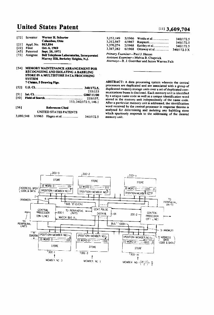
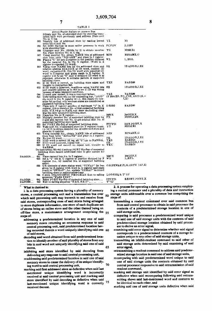
United States Patent [111 3,609,704 [72] Inventor Werner H- Schurter 3,252,149 5/1966 Weida et al.. ..... .. 340/1725 Columbus, Ohlo 3,312,947 4/1967 Raspanti .... .. 340/1725 [21] Appl. No. 863,894 3,370,274 2/1968 Kettley et al..... 340/1725 [22] Filed Oct. 6, 1969 3,387,262 6/1968 Ottaway et al .............. .. 340/1725 X [45] Patented Sept. 28, 1971 . . __ [73] Assignee Bell Telephone Laboratories, Incorporated Paflii‘nng'ga . k - . pmc Murray Hm’ Berkeky Hugh's’ NJ’ Anorneys- R. J. Guenther and James Warren Falk [54] MEMORY MAINTENANCE ARRANGEMENT FOR RECOGNIZING AND ISOLATING A BABBLING STORE IN A MULTISTORE DATA PROCESSING 5 Drawing Figs- ABS‘TRACT: A data processing system wherein the central processors are duplicated and are associated with a group of U.S. ...................................................... .. dup?cated memory storage units over a set ofduplicated cam 235/153 munications buses is disclosed. Each memory unit is identi?ed 1 In‘. ...................................................... u l a unique name code as wcu as a unique identi?cation word 0‘ .......................................... .. stored in the memory uni‘ independently of the name code‘ 153; 340/ 172.5, 146-1 After a particular memory unit is addressed, the identi?cation word received by the central processor in response thereto is [56] Rdemm” cued analyzed for determining and isolating any babbling store UNITED STATES PATENTS which spuriously responds to the addressing of the desired 3,080,548 3/l963 Hagen et a1 ................. .. 340/l 72.5 memory unit. 300-0 300-2 30o_ n STORE 10 WORD o ------ -- 00: x0 WORD 0 ------ -e mo 10 WORD 01:?“ 100K?‘ (ADDRESS, OPER) CODE’; DATA tposmora: MEMBER NO.) (POSITIONIMEMBER MOU (POSITIONlMEMBER NO) 2~ 4 1 ii 1 I 1 ?l To (ANSWER) A , | PERIPHERAL lBus "0"(EVEN) __;\_J|_ uws CENT. PULSE T CENTRAL TO PERIPHERAL PROCESSOR 2004 urms DISTR/B. CENTRAL i PROCESSOR ]-—-* MATCH BUS 9, -—~ - (OFFLINE) To II II PEBISRERAL } : BUS I (00mm Q L I I A \ 5 (ANSWER) ‘ ‘ l H I T- I l J i I ‘DADDR (POSITIONIMEMBER No.71 (POSITION: MEMBER NO? 7 ADDRESS —*— > ID WORD O - - - - - - " - OOI [D WORD O - " - - r - - -O|O icorgpi?mm) STORE STORE A l5100~J L300- 3 f 1 MEMBER NO 0 MEMBER N0 | MEMBER N0 1<rn2-l):
Transcript of (ADDRESS, OPER)
United States Patent [111 3,609,704
[72] Inventor Werner H- Schurter 3,252,149 5/1966 Weida et al.. ..... .. 340/1725 Columbus, Ohlo 3,312,947 4/1967 Raspanti .... .. 340/1725
[21] Appl. No. 863,894 3,370,274 2/1968 Kettley et al..... 340/1725 [22] Filed Oct. 6, 1969 3,387,262 6/1968 Ottaway et al .............. .. 340/1725 X [45] Patented Sept. 28, 1971 . . __
[73] Assignee Bell Telephone Laboratories, Incorporated Paflii‘nng'ga . k - . pmc
Murray Hm’ Berkeky Hugh's’ NJ’ Anorneys- R. J. Guenther and James Warren Falk
[54] MEMORY MAINTENANCE ARRANGEMENT FOR RECOGNIZING AND ISOLATING A BABBLING STORE IN A MULTISTORE DATA PROCESSING
5 Drawing Figs- ABS‘TRACT: A data processing system wherein the central processors are duplicated and are associated with a group of
U.S. ...................................................... .. dup?cated memory storage units over a set ofduplicated cam
235/153 munications buses is disclosed. Each memory unit is identi?ed 1 In‘. ...................................................... u l a unique name code as wcu as a unique identi?cation word
0‘ .......................................... .. stored in the memory uni‘ independently of the name code‘ 153; 340/ 172.5, 146-1 After a particular memory unit is addressed, the identi?cation
word received by the central processor in response thereto is [56] Rdemm” cued analyzed for determining and isolating any babbling store
UNITED STATES PATENTS which spuriously responds to the addressing of the desired 3,080,548 3/l963 Hagen et a1 ................. .. 340/l 72.5 memory unit.
300-0 300-2 30o_ n
STORE
10 WORD o ------ -- 00: x0 WORD 0 ------ -e mo 10 WORD 01:?“ 100K?‘ (ADDRESS, OPER) CODE’; DATA tposmora: MEMBER NO.) (POSITIONIMEMBER MOU (POSITIONlMEMBER NO)
2~ 4 1 ii 1 I 1 ?l To (ANSWER) A , | PERIPHERAL
lBus "0"(EVEN) __;\_J|_ uws CENT. PULSE T CENTRAL TO PERIPHERAL
PROCESSOR 2004 urms DISTR/B. CENTRAL i PROCESSOR ]-—-* MATCH BUS 9, -—~ - (OFFLINE)
To II II
PEBISRERAL } : BUS I (00mm Q L I I A \ 5 (ANSWER) ‘ ‘ l H I
T- I l J i I ‘DADDR (POSITIONIMEMBER No.71 (POSITION: MEMBER NO? 7 ADDRESS —*— > ID WORD O - - - - - - " - OOI [D WORD O - " - - r - - -O|O icorgpi?mm)
STORE STORE A l5100~J L300- 3
f 1 MEMBER NO 0 MEMBER N0 | MEMBER N0 1<rn2-l):
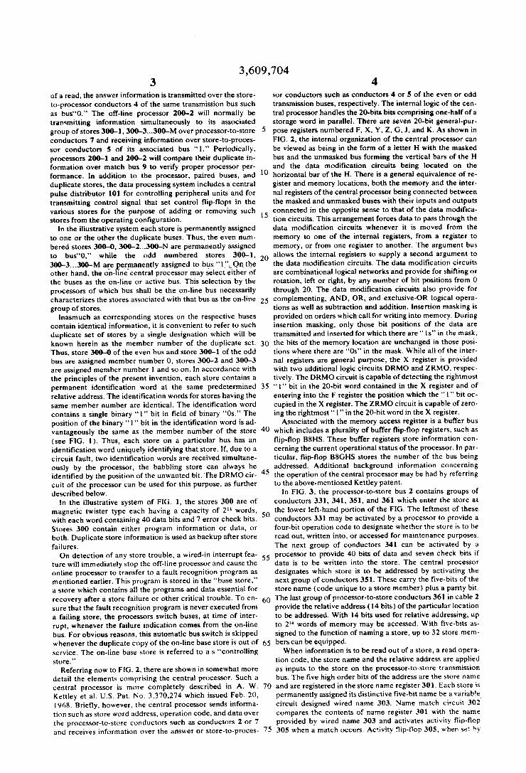
PATENTEDSEPZBIBII 3.609.704 sum 2 or 5
FIG. 2
CENTRAL PROCESSOR ZOO-l
BUFFER BUS TO FROM MEMORY MEIMORY REGISTERS
I A BUFFER BUS 7/: 2 5 Y i, 1
MEMORY ACCESS REGISTER \
I I I BBGHS
DATA MODIFICATION cmcuns MATCH __Tp OTHER
" REG. PROCESSOR
.WMATCH F REGISTERS BUS
I I DRMO ZRMQ V’T“ ARGUMENT BUS
I I X REG|STERS “"‘UNMASKED BUS
Y, Z,G,J AND K --a »—u
REGISTERS
FROM SCANNER
PAR -
T0 PULSE AND —--.- SIGNAL
I~"MASKED BUS DISTRIBUTORS
PATENTEDSEP28I97I 334609.704 sIIEET II M 5
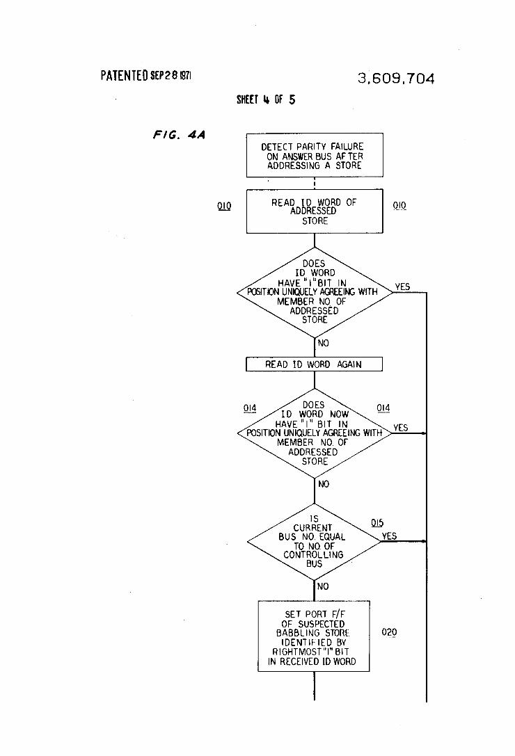
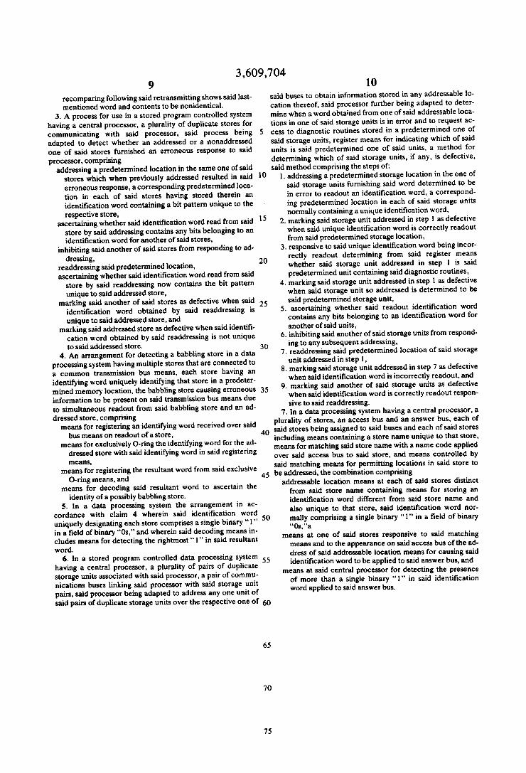
FIG. 4A DETEcT PARITY FAILURE ON ANSWER BUS AFTER ADDRESSING A STORE
0|0 READ ID WORD OF —- ADDRESSED
STORE
DOES ID WORD
HAVE "I"BIT IN POSITION uNIOuELY AGREEING WITH
MEMBER NO OF ADDREssED
sTORE
NO
[ READ ID woRD AGAIN
DOES '
—— ID WORD Now
HAVE "I" BIT IN POSITION UNIQUELY AGREEING WITH
MEMBER NO. OF ADDREssED
sTORE
IS CURRENT
BUS NO. EQUAL T0 NO OF
CONTROLLING BUS
sET PORT F/F OF SUSPECTED BABBLING STORE O29 IDENTIFIED BY
RIOI-ITMOST "l“ BIT IN RECEIVED ID WORD

PATENTED 8EP28 IBTI
FIG. 48
3.609.704 SHEET 5 BF 5
READ 1o woao 0F ORIGTNALLY ADDRESSED
STORE
ID woao NOW HAVE "I" BIT m
MEMBER NO. OF PREV. ADDRESSED
STORE
YES
POSITION UNIQUELY AGREEING WITH NO
READ ID WORD AGAIN
DOES 10 WORD NON
HAVE "I" BIT IN POSITION UNIQUELY AGREETNG WITH
MEMBER NO. OF PREV. ADDRESSED
UPDATE BIT OF STATUS WORD OF BABBLING
STORE TO IDENTIFY BABBLING
STORE TO SUBSEQUENT MAINT. ROUTINES
STORE
RESET PORT F/F OF SUSPECTED
BA BBLING STORE
"PASS EXIT" BABBLING STORE FOUND I
"FAIL EXIT" FAULT LIES m
ADDRESSED STORE OR 10 woao IS MUTILATED
3,609,704 1
MEMORY MAINTENANCE ARRANGEMENT FOR RECOGNIZING AND ISOLATING A BABBLING STORE IN
A MULTISTORE DATA PROCESSING SYSTEM
BACKGROUND OF THE INVENTION
This invention relates to memory storage arrangements in self-checking and/or self-diagnosing data processing systems and, more particularly, to systems in which a plurality of memory units are associated with some processing unit (s) 10 over a common bus transmission system.
In many data processing applications, the memory storage required for the data to be processed and the programming in structions for processing the data may be subdivided in several distinct memory units or “stores." This may be desirable for 15 various reasons: to separate instruction memory and data memory, to provide modular system design, to provide for fu tu re growth, or, in duplicated memory systems, to improve the chances of system recovery in the presence of multiple com ponent failures. 20 The reads instructions and data from, and writes data into,
the stores via a transmission bus. While the use of a direct bus from the processor to each store individually would make the selection of a store immune to store failures, the greater cost and space expenditure is often not justifiable. Instead, an ar- 2 5 rangement may be used in which the processor reads and/or writes into some or all stores via a common bus. A given store then responds only if it recognizes a word address as being in its address range. The address may comprise two groups of bits, the ?rst group designating the particular store and a 30 second group being the “relative address," i.e., the desired lo cation within the store.
Circuit component failures during writing, storing, or read ing of information can be detected by redundant bit infonna tion (error codes, parity), by duplication and data matching, 35 or special indicator leads. It is common practice to use the common bus for the checking information as well as the data.
Typically, detection of a store failure results in an interrupt of the normal data processing program. A fault-recognition program then identi?es the store containing the failure, takes 40 it out of service, returns 0 data processing, and in due time a diagnostic program identi?es the failing circuit, or circuit component.
It has been discovered that certain circuit failures in a store may cause this store to "babble," i.e., to respond to a read 45 command even though another store is addressed. The bab bling store sends answer information simultaneously with, and usually di?'erent from, the properly responding store (referred to as the "addressed store“). The resulting data appears muti lated at the processor end and will fail one or several error checks. In response, the fault recognition program suspects the addressed store and takes it out of service although it does not contain the failure. The babbling store, on the other hand, will remain in service. It will make successful diagnostics of the good store unreliable and, in addition, may cause other good stores to go out of service. While babbling-store failures are infrequent, the disruptive
effects which they can produce are a matter of serious con cern in self-checking systems. Heretofore, the only alternative 60 was provision of private checking paths to each individual store on a bus. This is not only expensive but difficult to imple ment in a system designed for future growth in memory size.
SUMMARY OF THE INVENTION
In accordance with the present invention, a procedure is fol lowed which precedes the running of conventional fault recog nition and diagnostic programs and whose purpose it is to determine whether a babbling store was the cause of the store
65
failure. This is done by reading of a special identi?cation word 70 located in the store which was being addressed when the bab bling occurred. In accordance with the invention. an identi? cation word unique to the store is permanently stored at the same relative address in each store of the memory system. Next, the central processor compares the identi?cation word 75
50
55
2 received with the word expected to be returned. If the com parison veri?es that the identi?cation word was returned cor rectly, normal maintenance procedures may safely be fol lowed inasmuch as no response from a nonaddressed store was obtained. However, if an incorrect identi?cation word was returned, the cause could either be a failure of the addressed store or the existence of a babbling store. According to the in vention, the structure of the identification in such that the processor, by analyzing its mutilated pattern, can directly identify the babbling store, if one exists, and temporarily disconnect it from the common bus. In order to deten'nine whether the store so identi?ed was in fact babbling, the identi?cation word of the addresses store is dien read again. If the correct identi?cation is not obtained, the suspected bab bling store is marked as being defective and a diagnostic pro gram scheduled for it. If the correct identi?cation word is not obtained, the addressed store may safely be marked as being defective and normal maintenance procedures should pin point the trouble.
Accordingly, a feature of the present invention is the analy sis of a mutilated identi?cation word obtained from one store to locate another store which exhibits a spurious response.
It is another feature of the present invention to mask from the identi?cation word obtained from the ?rst store all of the bits which correspond to the bits of the expected identi?cation word of that store and to identify such other store by analysis of any remaining unmasked bits.
It is another feature of the present invention temporarily to prevent such store identi?ed by the remaining unmasked bits from delivering any readout data to the common bus.
It is another feature of the present invention to determine that the initially addressed store is defective when, upon such readdressing, an incorrect identi?cation word continues to be obtained and, on the other hand, to determine that the tem porarily inhibited store was defective when a correct identi? cation word is obtained.
DESCRIPTION OF THE DRAWING
The foregoing and other features of the present invention may become more apparent by reading the following detailed description of one implementation of the invention, together with the drawing; in which:
FIG. 1 shows a block diagram of the duplicate processor, bus transmission system, and stores wherein each store has an identi?cation word stored therein for implementing the main tenance arrangement of the present invention;
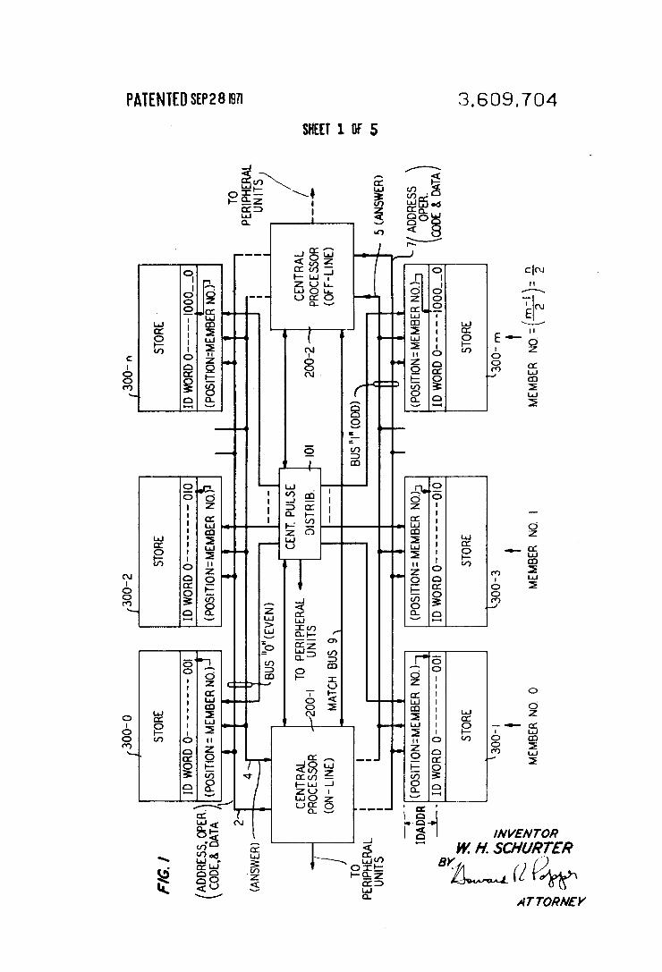
FIG. 2 shows a more detailed diagram of a central processor of FIG. 1;
FIG. 3 shows a simpli?ed diagram of the store having the identi?cation word of FIG. 1 stored therein; and
FIGS. 4A and 4B show a flow chart of an illustrative procedure for carrying out the maintenance arrangement of the present invention.
GENERAL DESCRIPTION
Referring to FIG. 1, a data processing system is shown in which, for purposes of achieving high operating reliability, certain equipments are duplicated. A pair of central proces sors 200-1 and 200-2 are shown associated with a pair of transmission buses by means of which the processors commu nicate with the plurality of stores 300. Within a bus, the con ductor leads are grouped according to their function. In nor mal operation, one of the central processors such as processor 200-1 will be “on-line“ or active, i.e., exercising control over the peripheral units (not shown), such as circuits to control and monitor a telephone switching network. Within either bus, the conductor leads are grouped according to their func tion. For example, the on-line central processor might trans mit the store address, along with a read, write or maintenance operation code and in case of a write, also the data to be stored, over the processor-to-store transmission conductors 2 to its associated group of stores 300-0, 300-2...300-N. ln case
3,609,704 3
of a read, the answer information is transmitted over the store to-processor conductors 4 of the same transmission bus such as bus“0." The off-line processor 200-2 will normally be transmitting information simultaneously to its associated group of stores 300-1, 300-3...300-M over processor-to-store conductors 7 and receiving information over store-to-proces sor conductors S of its associated bus “I." Periodically. processors 200-1 and 200-2 will compare their duplicate in formation over match bus 9 to verify proper processor per formance. In addition to the processor, paired buses, and duplicate stores, the data processing system includes a central pulse distributor 101 for controlling peripheral units and for transmitting control signal that set control flip-flops in the various stores for the purpose of adding or removing such stores from the operating configuration.
In the illustrative system each store is permanently assigned to one or the other the duplicate buses. Thus, the even num bered stores 300-0, 300—2...300-N are permanently assigned to bus"0," while the odd numbered stores 300-1, 300—3...300-M are permanently assigned to bus “lfV'LQn the other hand, the on-line central processor may select either of the buses as the on-line or active bus. This selection by the processors of which bus shall be the on-line bus necessarily characterizes the stores associated with that bus as the on-line group ofstores. Inasmuch as corresponding stores on the respective buses
contain identical information, it is convenient to refer to such duplicate set of stores by a single designation which will be known herein as the member number of the duplicate set. Thus, store 300-0 of the even bus and store 300-1 of the odd bus are assigned member number 0, stores 300-2 and 300-3 are assigned member number I and so on. in accordance with the principles of the present invention, each store contains a permanent identi?cation word at the same predetermined relative address. The identi?cation words for stores having the same member number are identical. The identi?cation word contains a single binary "I" bit in ?eld of binary “0s." The position of the binary “ l “ bit in the identi?cation word is ad vantageously the same as the member number of the store (see FIG. 1). Thus, each store on a particular bus has an identi?cation word uniquely identifying that store. If, due to a circuit fault, two identi?cation words are received simultane ously by the processor, the babbling store can always be identi?ed by the position of the unwanted bit. The DRMO cir cult of the processor can be used for this purpose, as further described below.
In the illustrative system of FIG. 1, the stores 300 are of magnetic twister type each having a capacity of 2H words, with each word containing 40 data bits and 7 error check bits. Stores 300 contain either program information or data, or both. Duplicate store information is used as backup after store failures. On detection of any store trouble, a wired-in interrupt fea
ture will immediately stop the off-line processor and cause the online processor to transfer to a fault recognition program as mentioned earlier. This program is stored in the “base store,“ a store which contains all the programs and data essential for recovery after a store failure or other critical trouble. To en sure that the fault recognition program is never executed from a failing store, the processors switch buses, at time of inter rupt, whenever the failure indication comes from the on-line bus. For obvious reasons, this automatic bus switch is skipped whenever the duplicate copy of the on-line base store is out of service. The on-line base store is referred to a s “controlling store.“
Referring now to FIG. 2, there are shown in somewhat more detail the elements comprising the central processor. Such a central processor is more completely described in A. W. Kettley et al. US. Pat. No. 3,370,274 which issued Feb. 20, I968. Brie?y, however, the central processor sends informa tion such as store word address, operation code, and data over the processor-to-store conductors such as conductors 2 or '7 and receives information over the answer or store-to-proces
25
30
35
40
45
50
55
60
65
70
75
4 sor conductors such as conductors 4 or 5 of the even or odd
transmission buses, respectively. The internal logic of the cen tral processor handles the 20-bits bits comprising one-half of a storage word in parallel. There are seven 20-bit general-pur pose registers numbered F, X, Y, Z, G, .l, and K. As shown in FIG. 2, the internal organization of the central processor can be viewed as being in the form of a letter H with the masked bus and the unmasked bus forming the vertical bars of the H and the data modi?cation circuits being located on the horizontal bar of the H. There is a general equivalence of re~ gister and memory locations, both the memory and the inter~ nal registers of the central processor being connected between the masked and unmasked buses with their inputs and outputs connected in the opposite sense to that of the data modi?ca tion circuits. This arrangement forces data to pass through the data modi?cation circuits whenever it is moved from the memory to one of the internal registers, from a register to memory, or from one register to another. The argument bus allows the internal registers to supply a second argument to the data modi?cation circuits. The data modi?cation circuits are combinational logical networks and provide for shifting or rotation, left or right, by any number of bit positions from 0 through 20. The data modi?cation circuits also provide for complementing, AND, OR, and exclusive-OR logical opera tions as well as subtraction and addition. Insertion masking is provided on orders which call for writing into memory. During insertion masking, only those bit positions of the data are transmitted and inserted for which there are “ ls“ in the mask; the bits of the memory location are unchanged in those posi tions where there are "05“ in the mask. While all of the inter nal registers are general purpose, the X register is provided with two additional logic circuits DRMO and ZRMO, respec— tively. The DRMO circuit is capable ofdetecting the rightmost “ l " bit in the 20-bit word contained in the X register and of entering into the F register the position which the “ l “ bit oc~ cupied in the X register. The ZRMO circuit is capable of zero in g the rightmost " l " in the 20-bit word in the X register.
Associated with the memory access register is a buffer bus which includes a plurality of buffer ?ip-flop registers, such as flip-?op BSHS. These buffer registers store information con cerning the current operational status of the processor. In par ticular, flip-?op B8GHS stores the number of the bus being addressed. Additional background information concerning the operation of the central processor may be had by referring to the above-mentioned Kettley patent. .
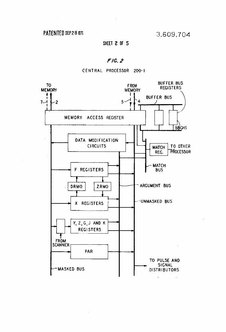
In FIG. 3, the processor-to-store bus 2 contains groups of conductors 331, 341, 351, and 361 which enter the store at the lower left-hand portion of the H0. The leftmost of these conductors 33] may be activated by a processor to provide a four-bit operation code to designate whether the store is to be read out, written into, or accessed for maintenance purposes. The next group of conductors 341 can be activated by a processor to provide 40 bits of data and seven check bits if data is to be written into the store. The central processor designates which store is to be addressed by activating the next group of conductors 351. These carry the ?ve-bits of the store name (code unique to a store member) plus a parity bit. The last group of processor-to~store conductors 361 in cable 2 provide the relative address ( 14 bits) of the particular location to be addressed. With 14 bits used for relative addressing, up to 2H words of memory may be accessed. With ?ve-bits as signed to the function of naming a store, up to 32 store mem bers can be equipped. When information is to be read out of a store, a read opera
tion code, the store name and the relative address are applied as inputs to the store on the processor-to-store transmission bus. The live high order bits of the address are the store name and are registered in the store name register 30]. Each store is permanently assigned its distinctive ?ve-bit name be a variable circuit designed wired name 303. Name match circuit 302 compares the contents of name register 301 with the name provided by wired name 303 and activates activity ?ip-?op 305 when a match occurs. Activity flip~?op 305, when set by
3,609,704 5
match circuit 302, enables AND gate 306. AND gate 306 al‘ lows the relative address registered in address register 307 to be applied to memory module access circuit 308. The word in memory module 309 at the addressed location is ampli?ed by readout circuit 310 and inserted into data register 311 from which it is normally applied on me store-to-processor conduc tors of its associated transmission bus. For the purpose of isolation in a complex trouble situation, the store may have PORT flip-?op 312 set by a signal from central pulse distribu tor (CPD) 101. When PORT ?ip-flop 312 is set, gate 313 is in hibited and prevents data register 311 from delivering its con tents to the answer leads of its associated store-to-processor bus. 0n write orders, operations are the same except that opera
tion-code register-decoder 315, in response to registering a write order, will activate write circuit 316 to write the data ap plied over the write data leads of the processor-to-store bus into memory module 309. For the purpose of a special diag nostic test, the bus-register test, AND gates 320 and 321 can be enabled to pass the contents of name register 301 and ad dress register 307 directly to data register 311 and thence back to the processor over the answer conductors of the store to-processor bus. During the bus-register test, the central processor can verify, among other things, whether the store correctly registered the transmitted name bit pattern.
Problem of the Babbling Store (see FIG. 3)
From the above description of FIG. 3, it is seen that the ?ve name bits designating a particular store must be correctly received and registered in name register 301. if the name re gister 301 of a store which is addressed does not correctly re gister these bits, the addressed store will not be accessed because name match circuit 302 will not recognize the correct bit pattern in register 301. On the other hand, if the name re gister 301 of a nonaddressed store incorrectly registers a name bit pattern in such a way that they appear to be the same as that in wired name 303, name match circuit 302 will allow the memory module 309 in this nonaddressed store to be inter rogated even though the name bits transmitted on the name bit leads of bus 2 did not agree with the name pattern in wired name 303. Under these latter circumstances, the store will “ babble” in the sense described earlier. In either case, the response received by the processor will be the responses of two stores OR’d together, and error checks in the processor will fail. '
Upon such a parity failure detection, the central processor in the prior art system would take the originally addressed store out of service and execute a diagnostic program on it. in this program, the central processor would ?rst run a bus-re gister test, i.e., it will once again address the same store, but in addition it will transmit a signal to operate gate 320 in the ad dressed store. This causes the name bits registered in register 301 to be transmitted directly to data register 311 and thence back to the processor. The outcome of the bus-register test de pends on the component failure which causes babbling. Ifthe failure is in the name register of the babbling store, the bus-re gister test fails since it explicitly tests the name register. The diagnostic result would pinpoint the failure to the proper cir cuit but to the wrong store, since the addressed store is not the store which babbles. On the other hand, a store might have babbled because of a
defect in the diode matrix of its name match circuit or in cer tain gating operations, so that its active ?ip-flop is erroneously set although the name register works correctly. Since the bus register test does not use the affected circuit, it would pass. Depending on the exact structure of the remaining diagnostic tests, they either would all pass, or would fail with diagnostic output locating the failure both in the wrong store and the wrong circuit. 1
Regardless of whether the addressed store is le? in service
20
25
30
35
45
55
65
70 .
6 or not, store failures will continue to be caused by the bab bling store in the working con?guration of the prior art system. Each time, this causes a program interrupt which often involves automatic bus switching, as explained earlier,‘ with its inherent hazard to program sanity. In addition, the complete diagnostic program will be called after each failure and each time takes up to several minutes to run. During this time, store duplication is lost, and system reliability is seri ously jeopardized. Thirdly, the babbling store must be taken out of service by the operator’s action since the maintenance programs are incapable of isolating a babbling store. Finally, diagnostic results will be unreliable.
Referring now to FIG. 4, there is shown a flow chart of the process of the present invention by means of which a babbling store is recognized and isolated in the illustrative system. The steps of the process may be implemented by a sequence of stored programmed instructions, which in the ensuing descrip tion will be assigned reference numbers so that the detailed steps hereinafter described may be correlated with the ?ow chart of FIG. 4. For each numbered step hereinafter there will also be given a mnemonic operation code as actually em ployed in one illustrative embodiment of the invention. The instructions constituting the steps of the process hereinafter described, as well as any data needed, are assumed to be stored in the base stores. When the processor detects a store failure, it may advantageously use the high order or name bits of the address which resulted in the store failure as an index to a translation table to obtain the unit number of the store which was addressed when the parity failure was detected.
in instruction 020, the PORT ?ip-?op of the suspected bab bling store is set. This isolates the suspected store from its answer bus for all reading. if the suspected store is the con trolling store, setting the PORT ?ip-?op would result in pro gram insanity. In this case, the assumption is made that no babbling store is involved. This is acceptable, because if the duplicate copy of the controlling store had been in service, an automatic bus switch would have occurred, and the suspected store would no longer be the controlling store. So, since the duplicate copy is out of service, no recovery would be possible if the controlling store was in fact babbling. in order to deter mine whether the suspected store is the controlling store, in struction 015 compares a memory bit CSB which indicates the current controlling store bus with the flip-?op BBGHS which indicates the bus number of the addressed store.
In the ensuing description of an illustrative program sequence which implements the process of the present inven tion, it will be assumed at the outset that the hardware cir cuitry has detected a failure upon receiving the response from an addressed store. Each step of the illustrative sequence is separately identified at the left by a three digit number such as 003. To the right of this number is given a brief English lan guage description of the step. To the right of the description is set forth the mnemonic of the instruction which consists of the mnemonic operation code, such as “Y2" in step 003. To the right of the operation code, and separated therefrom by a short space, is a combined data address and option ?eld by means of which additional information concerning the opera tion to be performed is speci?ed. For purposes of achieving greater clarity, the ensuing description will be presented in tabular form in table I. For the purposes of simplifying the description, it has been
thus far assumed that the procedure for determining whether a babbling store contributed an erroneous response was in itiated by a store failure detected by the processor in the course of processing useful data. However, such procedure can also be initiated in the course of systematic store tests, ex ecuted either due to failures other than store failures, or as preventive maintenance. The procedure for identifying the babbling store as described herein may advantageously be ex ecuted as the ?rst portion of such store tests. Further and other variations will be apparent to those skilled in the art
5 without departing from the spirit and scope of the invention.
BABBliL _.
3,609,704
TABLE I
Detect Parity Failure on Answer Bus Obtain unit No. of addressed store by entering trans- . lation table with previously used address. Place unit No. in Y reg. Identity bus of addressed store by reading lowest order bit of unit No. Set GHS ?ip~ilop to cause active processor to work with identi?ed bus. Truncate unit No. (divide by 2) to obtain member No. Place member No. in G reg. Using member No. obtain NAME bits of addressed store from table “B2NAME” and place in I register. Place a "1” bit into Z register in the position dictated by the member No. in the G register. (Word in Z register is expected ID word). Using store N AME bits for the addressed store and relative address IDADDR oi ID word, readout ID word, exclusive-0R, this ID word with expected ID word in Z register and place result in X register. X register will be all "0" only it obtained ID word is as expected, otherwise X contains pattern of suspected babbling stores. If ID word is correct, no babbling store exists and transfer to instruction 043. If ID word is incorrect, re-address usin NAME bits and relative address M in 010 to see if D was wrong because of some transient condition.
003
005
007
010
(111
012
Y Z
PCPDV
YG
MIN
WZ
SX IDADDRJJBZ
BARBER)
IDADDRJJEZ
014 Ii word now correct, it was a transient failure. 7 .7 . 'I‘XZ BABE!!!) 015 If the [ailing store was on the controlling bus, "AND" IF BBUHSHEQWCSB, AND (X.
the word in the X register w/—1, this clears the low l,X) order bit so that only nonbase stores are considered as suspected babbling stores. Place into F register position of rightmost “1" in X register, this is member No. of ?rst suspected babbling store. ii X=0 go to FAIL exit since controlling store was the only suspected babbling store. Placebus No.inXregister.__.. Multiply member No. oi’ suspected babbling store by 2 and add current bus No. to get original unit No. of Suspected babbling store back. Set PORT ?ip-?op of suspected babbling store, . Take unit No 01’ addressed store (in Y register] trunc. (-l- by 2) to obtain member N0. of addressed store and lace in G register. ‘sing member No., obtain NAME bits of addressed
store from table “B2NAME" and place in J register. Re-test ID word _ _ _ . . . _ _ . _ _ _ . _ . . _ _ . .. ,
If iD word is correct (K reg. all "0") go to BABBIO. . if H) word incorrect, repeat test_____ _ _ . _ _ . . , . l . .
1i 1]) word not correct on repeat test. transfer to BABB2D.
Do instruction 031-041 ii setting PORT ilip~iiop oi suspected babgling store caused addressed store to give correct 11) war .
031 Place current bus No. in Z register.-. .. l. 032 Set a "1" bit in G register in position dictated by F
register 0.43., by member No. of suspected babbling store). 0R contents oi store status word “STMAP” for bus given by Z 1' star with word in G register and place result in "ST AP”, i.e., update "STMAP’ to record babbling store as maintenance-busy. CALL DIAGNOSTIg?rROGRAM Exit to calling
017
018 019
020 022
033
DRMO
MBVE FX
ETC PD
MIN
SK TKZ SK TKU
MDV E G
BABBZiO
20
B2NAME,G
IDADDPLLEZ BABBIO IDADDILLEZ BABB20
034 sequence “PASS EXI
042 Reset PORT ?ip-?op of suspected babbling storm . i 043 Exit to calling sequence “FAIL EXIT" . . . . N . .
STCPD RESET.PORT,X BABB20. .
T‘ 0,1 BABB30 . _
What is claimed is: l. in a data processing system having a plurality of memory
stores, a ccntral processing unit and a transmission bus over which said processing unit may transmit to and receive from said stores, corresponding ones of said storcs being arranged to store duplicate information, one store of each duplicate set of stores being an onlinc store and the other thereof being an
2. A process for operating a data processing system employ ing a central processor and a plurality of data and instruction storage units addressable over a common bus comprising the steps of: _ _‘
transmitting a readout command over said common bus from said central processor to obtain in said processor the contents of a predetermined storage location in one of
50
received thcrcat.
o?-linc store, a maintenance arrangement comprising the 5 5 said storage units, steps of: comparing in said processor a predetermined word unique
addressing a Pfedclemlined location in all)’ one of Said to said one of said storage units with the contents of said memory stores returning an erroneous response to said predetermined storage location obtained by said proces ccntral processing unit, said predetermined location hav- so: to derive an enor signal, ing recorded therein a word uniquely identifying said one 60 examining said error signal to determine whcthcr said signal of said stores, corresponds to a predetermined contents of a storage lo
dccoding said word obtained from said predetermined loca- cation unique to any other of said storage units, tion to identify another of said plurality of stores from any transmitting an inhibit-readout command to said other of bits in said word not uniquely identifying said one of said said storage units determined by said examining of said stores, 65 error signal,
inhibiting said store identi?ed by said decoding from rctransmitting a readout command to address said predeter delivcring any response to said central processing unit, mincd storage location in said one of said storage units,
readdrcssing said predetermined location in said one of said recomparing with said predetermined word unique to said memory stores to cause the delivery of its unique identify- one of said storage units the contents obtained by said ing word to said central processing unit, 70 central processor responsive to said retransmission of said
marking said ?rst addressed store as defective when said last readout command, mentioned unique identifying word is incorrectly marking said storage unit identified by said error signal as received at said central processing unit and marking said defective when said rccompan'ng following said retrans storc identi?ed by said decoding as defective when said mitting shows said last-mentioned word and contents to last-mentioned unique identifying word is correctly 75 be identical to each other, and
marking said one of said storage units defective when said
3,609,704
recomparing following said retransmitting shows said last mentioned word and contents to be nonidentical.
3. A process for use in a stored program controlled system having a central processor, a plurality of duplicate stores for communicating with said processor, said process being adapted to detect whether an addressed or a nonaddressed one of said stores furnished an erroneous response to said
processor, comprising addressing a predetermined location in the same one of said
stores which when previously addressed resulted in said erroneous response, a corresponding predetermined loca tion in each of said stores having stored therein an identi?cation word containing a bit pattern unique to the respective store,
ascertaining whether said identi?cation word read from said store by said addressing contains any bits belonging to an identi?cation word for another of said stores,
inhibiting said another of said stores from responding to ad dressing,
readdressing said predetermined location, ascertaining whether said identi?cation word read from said
store by said readdressing now contains the bit pattern unique to said addressed store,
marking said another of said stores as defective when said identi?cation word obtained by said readdressing is unique to said addressed store, and
marking said addressed store as defective when said identi? cation word obtained by said readdressing is not unique to said addressed store.
4. An arrangement for detecting a babbling store in a data processing system having multiple stores that are connected to a common transmission bus means, each store having an identifying word uniquely identifying that store in a predeter mined memory location, the babbling store causing erroneous information to be present on said transmission bus means due to simultaneous readout from said babbling store and an ad dressed store, comprising means for registering an identifying word received over said
bus means on readout of a store, means for exclusively O-ring the identifying word for the ad
dressed store with said identifying word in said registering means,
means for registering the resultant word from said exclusive O-ring means, and
means for decoding said resultant word to ascertain the identity of a possibly babbling store.
5. [n a data processing system the arrangement in ac cordance with claim 4 wherein said identi?cation word uniquely designating each store comprises a single binary “ l " in a ?eld of binary "0s," and wherein said decoding means in cludes means for detecting the rightmost “ l“ in said resultant word.
6. In a stored program controlled data processing system having a central processor, a plurality of pairs of duplicate storage units associated with said processor, a pair of commu nications buses linking said processor with said storage unit pairs, said processor being adapted to address any one unit of said pairs of duplicate storage units over the respective one of
20
25
30
35
40
45
50
60
65
70
75
10 said buses to obtain information stored in any addressable lo cation thereof, said processor further being adapted to deter mine when a word obtained from one of said addressable loca tions in one of said storage units is in error and to request ac cess to diagnostic routines stored in a predetermined one of said storage units, register means for indicating which of said units is said predetermined one of said units, a method for determining which of said storage units, if any, is defective, said method comprising the steps of:
. addressing a predetermined storage location in the one of said storage units furnishing said word determined to be in error to readout an identi?cation word, a correspond ing predetermined location in each of said storage units nonnally containing a unique identi?cation word,
2. marking said storage unit addressed in step I as defective when said unique identi?cation word is correctly readout from said predetermined storage location,
3. responsive to said unique identi?cation word being incor rectly readout determining from said register means whether said storage unit addressed in step l is said predetermined unit containing said diagnostic routines,
4. marking said storage unit addressed in step 1 as defective when said storage unit so addressed is determined to be said predetermined storage unit,
5. ascertaining whether said readout identi?cation word contains any bits belonging to an identi?cation word for another of said units,
6. inhibiting said another of said storage units from respond ing to any subsequent addressing,
7. readdressing said predetermined location of said storage unit addressed in step i,
8. marking said storage unit addressed in step 7 as defective when said identi?cation word is incorrectly readout, and
9. marking said another of said storage units as defective when said identi?cation word is correctly readout respon sive to said readdressing.
7. In a data processing system having a central processor, a plurality of stores, an access bus and an answer bus, each of said stores being assigned to said buses and each of said stores including means containing a store name unique to that store, means for matching said store name with a name code applied over said access bus to said store, and means controlled by said matching means for permitting locations in said store to be addressed, the combination comprising
addressable location means at each of said stores distinct from said store name containing means for storing an identi?cation word different from said store name and also unique to that store, said identi?cation word nor mally comprising a single binary “1" in a ?eld of binary “0s,"a
means at one of said stores responsive to said matching means and to the appearance on said access bus of the ad dress of said addressable location means for causing said identi?cation word to be applied to said answer bus, and
means at said central processor for detecting the presence of more than a single binary “1" in said identi?cation word applied to said answer bus.