
Additive Manufacturing Methods and Materials Requirements ...
10
Additive Manufacturing Methods and Materials Requirements for the Fabrication of 3D Printed Hybrid Electronic Circuits D. R. Hines Laboratory For Physical Sciences College Park, MD, USA [email protected] (L1) Thermal processing up to 250 ˚C. (L2) Fabrication on flat surfaces. (L3) Surface mounted electronic components. Current Fabrication Limitations: Needed Fabrication Improvements: Develop Fabrication Methods for the Elimination of Surface Mounted (SMT) Electrical Components for Electronic Circuit Fabrication. Direct-Write Printing Limitations and Needed Improvements Platform Demonstrators: • LPS Power Supply • LM Micro-Controller (1) Identify & characterize ink materials that can be processed at temperatures below 150 ˚C without loss in performance. (2) Develop printing methods for the fabrication of circuits onto non-flat, 3D printed surfaces. (3) Develop methods for integrating/embedding components into circuits during fabrication. Object:
Transcript of Additive Manufacturing Methods and Materials Requirements ...
Additive Manufacturing Methods and Materials Requirements for the Fabrication
of 3DPrinted Hybrid Electronic Circuits
D. R. HinesLaboratory For Physical Sciences
College Park, MD, [email protected]
(L1) Thermal processing up to 250 ˚C.
(L2) Fabrication on flat surfaces.
(L3) Surface mounted electronic components.
Current
Fabrication
Limitations:
Needed
Fabrication
Improvements:
Develop Fabrication Methods for the Elimination
of Surface Mounted (SMT) Electrical Components for Electronic Circuit Fabrication.
Direct-Write Printing Limitations and Needed Improvements
Platform Demonstrators:• LPS Power Supply • LM Micro-Controller
(1) Identify & characterize ink materials that can be
processed at temperatures below 150 ˚C
without loss in performance.
(2) Develop printing methods for the fabrication of
circuits onto non-flat, 3D printed surfaces.
(3) Develop methods for integrating/embedding
components into circuits during fabrication.
Object:

1. Deposition rate Rpp > 0.001 mm3/sec with the ability to establish a desired rate.
2. > 3 hours stable deposition rate (DR < 10%) with no more than one purge per hour.
3. Feature sizes down to 20 μm and surface roughness (Dh)< 10% of layer thickness (h).
4. In-situ and/or post processing at temperatures < 150 ˚C.
5. Resistivity < 6×10⁻⁸ Ωm for conducting inks. Good electrical insulation for dielectric inks. Dimensional stability for structural inks.
6. Adhesion good enough to pass scotch tape test.
7. Also need automatic calculation of total Volume (V) and total Length (L) to be printed for a given print file (this allows determination of desired Deposition Rate (R) and print Speed (s) for the file).
Minimum Processability Requirements of Ink Materialsfor Direct-Write Manufacturing (related to AJ printing)
Design Requirement
LPS Power Supply Circuit - Single Room layout
List of main components:(a) Capacitors: 10 µF & 20 µF(b) Resistors: KΩ(c) Si IC chip: (d) Inductor: µH

64-Pin QFP µC
J-TAG
Conn
3V Battery
ON/OFF Switch
LED Display
Sensor
I/O
(+)
C1
LM Micro-Controller Circuit
List of main components:
(c) Capacitors: 0.1 µF (d) Resistors: 220Ω to 50KΩ
(a) LEDs(b) Si IC chip
LPS Power Supply
~1 mm
Circuitization:Aerosol-Jet Printed using
Ag-N Ink for Conducting Layers &
P-PI ink for Dielectric Layer
AJ Printed onto Polyimide coated SiO2/Si Substrate.
Processing temperature 255 °CComponents : Surface Mounted~(15 x 20) mm
13 Working Boards• Functional Test process (Room Temp)• 24 Hr ESS Temp Cycling• 96 Hr High temp Burn-in• Functional Test process (Room temp)
Over 4000 hrs of Thermal Cycling &Accelerated Life Testing
As Printed Circuitization
Populated Circuit
Input:5 Volts1 Amp

Requirements of Embedded/Integrated Components
Requirements:• Processing Temperature < 150
with no loss in material performance.
• Printed Circuitization (previously demonstrated).
• Printed Interconnects to Bare die IC chips with smooth transitions between different leveled surfaces.
• Resistors for 200 Ω to 160 K Ω
• Capacitors up to 20 µF (consider bare die Si-based caps).
• Inductors in the µH range with Q-factor > 10.
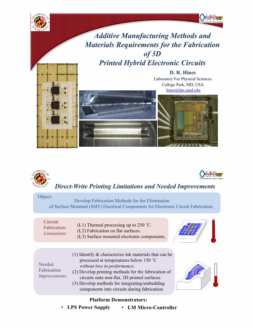
Line Pitch Pyramid
Examples of AJ Printed Structures with in-situ curing of UV-curable Polymer Ink
1mm
Tubes(black streak is felt marker note on back surface of glass subst.)
Note: aspect ratio for smallest cylinder Þ 2.8Cylinders
~1 mm Sq Base
5 mm long traces
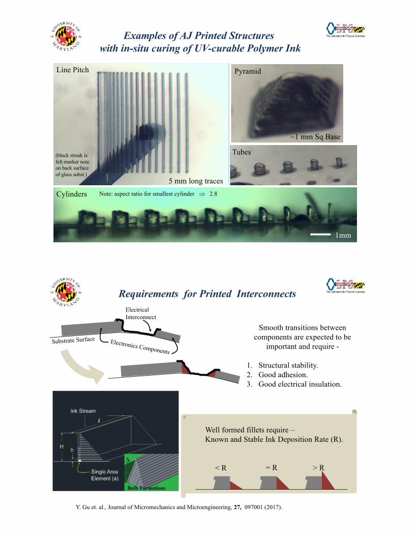
Smooth transitions between components are expected to be
important and require -
1. Structural stability.2. Good adhesion.3. Good electrical insulation.
Substrate Surface Electronics Components
ElectricalInterconnect
Well formed fillets require –Known and Stable Ink Deposition Rate (R).
< R > R= R
Y. Gu et. al., Journal of Micromechanics and Microengineering, 27, 097001 (2017).
Requirements for Printed Interconnects

AJ Printed Interconnects-over-Fillets
1 mm fillet 375 um fillet
Y. Gu et. al., Advanced Materials Technologies, 2 (2017).
Fillet – edge on views
Bare Si IC Chip with AJ Printed Interconnects
LM µ-Controller Chip
Close up image of Interconnects-over-Fillets
100 µm

LM u-Controller Circuit with Integrated Bare Si IC Chip
as printed
after SMT component attach
10 mm
AJ Printed Resistors

PS Circuit with Si based Capacitors as Substrate
~(15 x 20) mm
3.3μF/sq
2. Interconnects & Jumpers
3. Original PSCS
1. 4X8 Caps Substrate
AJ Printed Inductors
Polymer-Core, Straight SolenoidPlanar-Spiral
Ferrite-Core Iron-Core

AJ Printed InductorsPolymer-Core, Tapered Solenoid
Simulated and measured Results of AJ Printed Inductors
! "#$%&'>! "(')*($+ > ! -&#)%)+./0 "#$%&' < ./0 "(')*($+ < ./0 -&#)%)+
234 = 128 9 : ;
Q-factorOperating Frequency

Summary of Embedded/Integrated Components for Electronic Circuit Fabrication.
ResultsComponent Material(s) Status
Circuitization AJ printed Ag ink & Polymer ink
DemonstratedIntegrated into PS & uC
tested (PS - TC & HTOL)
Resistors AJ printed Carbon based resistor paste
Demonstrated
Capacitors Si based 3.3 uF Capacitors DemonstratedWorking to integrate into PS
Inductors AJ printed Ag ink w/ polymercore
Demonstrated
Si Bare IC chips Interconnect electrical attach to 300 um thick
bare die
DemonstratedIntegrated into uC
Interconnects AJ printed Ag ink over polymer fillets
DemonstratedIntegrated into uC
Test sample - in TC testing
Summary of Demonstrated AJ Printed ComponentsCapacitor Substrate
Printed Resistors
Printed Solid-core Inductors
Printed Interconnects-over-Fillets with Bare Si IC chips