Adatkonverterek: az analóg 'átjáró'
15
Test your EQ (Engineering Quotient)® 53 ______________________________________________________________________________________ Példák adatlap részletek (részletes adatlap: Internet link ) Mixed-signal technology means blending digital with the analog world, which is more like black magic . It's not just ones and zeroes, but things like tweaking voltages and currents - a lot of physics - and getting a number of different variables to mesh. [B. Runyan] Both technical skills (e.g., data converter and amplifier design) and system skills (e.g., functional partitions and tradeoffs) are required to develop useful products for leading edge applications. [McAdam] Don't underestimate the amount of work required to understand the data sheet and implement the interface. [S. Hendrix] 1: Resistor ladder 1 DAC LTC1599 (16 bit multiplying) 2: Current-steering 2 DAC LTC1668 (16 bit, 50 MSPS) 3: Interpolating DAC 3 AD9772A (14 bit, 160 MSPS) 4: SAR 4 ADC MAX1290 (12 bit, 400 KSPS) 5: Parallel 5 SAR ADC architecture SPT7938 (12 bit, 40 MSPS) 6: Pipeline 6 ADC AD9203 (10 bit, 40 MSPS) 7: Pipeline ADC w/ FIFO 7 THS1206 (12 bit, 6 MSPS) 8: ∆Σ combined 8 w/ pipeline ADC AD9260 (16 bit, 2.5 MSPS) 9: ADC does frequency translation 9 10: DAC using multi-bit ∆Σ modulation (14 bit, 10 MSPS) 10 1 ellenállás („R/2R”) hálózat: ”inverz” létra, szegmentálás – lásd 44. oldal 2 kapcsolt áram-források, szegmentálás – lásd 45. oldal 3 alapsávi ill. képmás rekonstrukció 4 fokozatos érték-közelítés– lásd 48. oldal (kapacitív belső D/A) 5 időben átlapolt működés ( „time interleaving” ) 6 konkurrens minta-kezelés – lásd 49. oldal 7 plusz több csatornás szimultán mintavétel 8 lásd 2.6b feladat (az OSADC és Nyquist-rate technikák kombinálása) 9 kontrollált alulmintavételezés 10 4-ed rendű (L = 4), multi-bites, digitális delta-szigma modulátor
Transcript of Adatkonverterek: az analóg 'átjáró'

Test your EQ (Engineering Quotient)® 53 ______________________________________________________________________________________
Példák adatlap részletek (részletes adatlap: Internet link)
Mixed-signal technology means blending digital with the analog world, which is more like black magic. It's not just ones and zeroes, but things like tweaking voltages and currents
- a lot of physics - and getting a number of different variables to mesh. [B. Runyan]
Both technical skills (e.g., data converter and amplifier design) and system skills (e.g., functional partitions and tradeoffs) are required to develop useful products
for leading edge applications. [McAdam]
Don't underestimate the amount of work required to understand the data sheet and implement the interface. [S. Hendrix]
1: Resistor ladder1 DAC LTC1599 (16 bit multiplying) 2: Current-steering2 DAC LTC1668 (16 bit, 50 MSPS) 3: Interpolating DAC3 AD9772A (14 bit, 160 MSPS) 4: SAR4 ADC MAX1290 (12 bit, 400 KSPS) 5: Parallel5 SAR ADC architecture SPT7938 (12 bit, 40 MSPS) 6: Pipeline6 ADC AD9203 (10 bit, 40 MSPS) 7: Pipeline ADC w/ FIFO7 THS1206 (12 bit, 6 MSPS) 8: ∆Σ combined8 w/ pipeline ADC AD9260 (16 bit, 2.5 MSPS) 9: ADC does frequency translation9 10: DAC using multi-bit ∆Σ modulation (14 bit, 10 MSPS)10
1 ellenállás („R/2R”) hálózat: ”inverz” létra, szegmentálás – lásd 44. oldal 2 kapcsolt áram-források, szegmentálás – lásd 45. oldal 3 alapsávi ill. képmás rekonstrukció 4 fokozatos érték-közelítés– lásd 48. oldal (kapacitív belső D/A) 5 időben átlapolt működés ( „time interleaving” ) 6 konkurrens minta-kezelés – lásd 49. oldal 7 plusz több csatornás szimultán mintavétel 8 lásd 2.6b feladat (az OSADC és Nyquist-rate technikák kombinálása) 9 kontrollált alulmintavételezés 10 4-ed rendű (L = 4), multi-bites, digitális delta-szigma modulátor

54 ADATKONVERTEREK ______________________________________________________________________________________
1: LTC1599 − 2-byte parallel input, low glitch 16-bit Multiplying DAC On-chip 4-Quadrant resistors Asynchronous clear pin resets to Zero scale or Mid-scale DNL and INL: 1LSB Max http://www.linear.com/ Application Note #86:
A Standards Lab Grade 20-Bit DAC with 0.1ppm/° Drift (http://www.linear.com/pub)
virtual ground (!)

Test your EQ (Engineering Quotient)® 55 ______________________________________________________________________________________
2: LTC1668 − 16-bit, 50MSPS differential current output DAC Laser trimmed, thin-film resistors High spectral purity: 87dB SFDR at 1MHz fOUT; 5pV-s glitch impulse http://www.linear.com/
56 ADATKONVERTEREK ______________________________________________________________________________________
3: AD9772A − 14-bit, 160 MSPS segmented current source DAC Optimized for baseband or IF waveform reconstruction applications 67.5 MHz Reconstruction Passband @ 160 MSPS; 74 dBc SFDR @ 25 MHz 2x Interpolation Filter with High- or Low-Pass Response 73 dB Image Rejection “Zero-Stuffing” Option for Enhanced Direct IF Performance Internal 2x/4x Clock Multiplier http://www.analog.com/ Interactive Design Tool: Harmonic Images in the AD9772 DAC
http://www.analog.com/techSupport/designTools/interactiveTools/index.html The AD9772A is a complete, 2x oversampling DAC that includes a 2x interpolation filter, a phase-locked loop (PLL) clock multiplier and a 1.20 V bandgap voltage reference.
While the AD9772A’s digital interface can support input data rates as high as 160 MSPS, its internal DAC can operate up to 400 MSPS, thus providing direct IF conversion capabilities. The 14-bit DAC provides two complementary current outputs whose full-scale current is determined by an external resistor. The AD9772A features a flexible, low jitter, differential clock input providing excellent noise rejection while accepting a sine wave input. An on-chip PLL clock multiplier produces all of the necessary synchronized clocks from an external reference clock source. Separate supply inputs are provided for each functional block to ensure optimum noise and distortion performance. A SLEEP mode is also included for power savings. Preceding the 14-bit DAC is a 2x digital interpolation filter that can be configured for a low-pass (i.e., baseband mode) or high-pass (i.e., direct IF mode) response. The input data is latched into the edge-triggered input latches on the rising edge of the differential input clock and then interpolated by a factor of two by the digital filter. For traditional baseband applications, the 2x interpolation filter has a low-pass response.
For direct IF applications, the filter’s response can be converted into a high-pass response to extract the higher image. The output data of the 2x interpolation filter can update the 14-bit DAC directly (NRZ mode) or undergo a “zero-stuffing” process (RZ mode) to increase the DAC update rate by another factor of two. This action enhances the relative signal level and pass-band flatness of the higher image.
Test your EQ (Engineering Quotient)® 57 ______________________________________________________________________________________
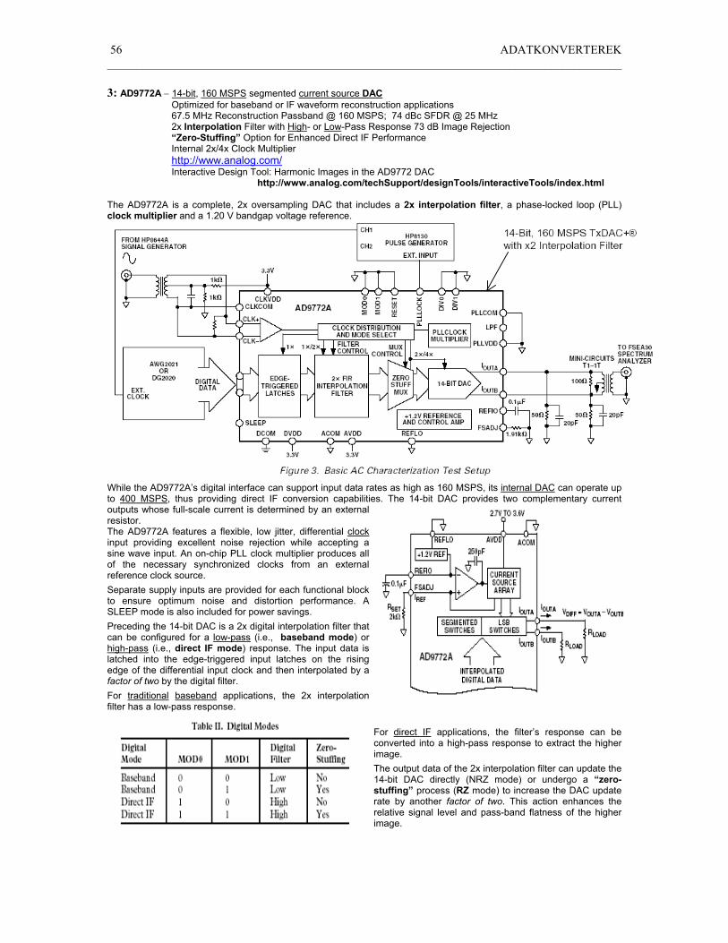
AD9772A - BASEBAND Referring to Figure 5, the “new” first image associated with the DAC’s higher data rate after interpolation is “pushed” out further relative to the input signal, since it now occurs at 2xfDATA – fFUNDAMENTAL. The “old” first image associated with the lower DAC data rate before interpolation is suppressed by the digital filter. As a result, the transition band for the analog reconstruction filter is increased, thus reducing the complexity of the analog filter. Furthermore, the sin(x)/x roll-off over the original input data passband (i.e., dc to fDATA/2) is significantly reduced. AD9772A - DIRECT IF As previously mentioned, the 2x interpolation filter can be converted into a high-pass response, thus suppressing the “fundamental” while passing the “original” first image occurring at fDATA – fFUNDAMENTAL. Figure 6 shows the time and frequency representation for a high-pass response of a discrete time sinewave. This action can also be modeled as a “1/2 wave” digital mixing process in which the impulse response of the low-pass filter is digitally mixed with a square wave having a frequency of exactly fDATA/2. [ Since the even coefficients have a zero value (refer to Table I), this process simplifies into inverting the center coefficient of the low-pass filter (i.e., invert H(18)). Note that this also corresponds to inverting the peak of the impulse response shown in Figure 2a. The resulting high-pass frequency response becomes the frequency inverted mirror image of the low-pass filter response shown in Figure 2b. ] It is worth noting that the “new” first image now occurs at fDATA + fFUNDAMENTAL. A reduced transition region of 2x fFUNDAMENTAL exists for image selection, thus mandating that the fFUNDAMENTAL be placed sufficiently high for practical filtering purposes in direct IF applications. Also, the “lower sideband images” occurring at fDATA – fFUNDAMENTAL and its multiples (i.e., N x fDATA – fFUNDAMENTAL) experience a frequency inversion while the “uppersideband images” occurring at fDATA + fFUNDAMENTAL and its multiples (i.e., N x fDATA + fFUNDAMENTAL) do not.
58 ADATKONVERTEREK ______________________________________________________________________________________
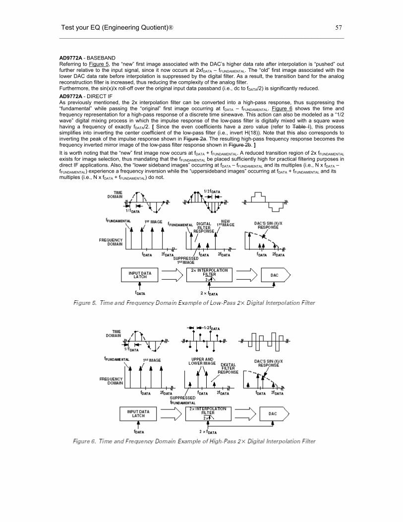
4: MAX1290 − 12-bit, 400 KSPS successive approximation (SAR) ADC Byte-wide parallel interface Automatic power-down, fast wake-up (2µs) http://www.maxim-ic.com/ Application Note #270: Analog-Signal Data Acquisition in Industrial Automation Systems http://www.maxim-ic.com/appnotes.cfm/appnote_number/270
Power consumption is only 10mW (VDD = VLOGIC) at a 400ksps max sampling rate. Two software-selectable power-down modes enable the MAX1290 to be shut down between conversions; accessing the parallel interface returns them to normal operation. Powering down between conversions can cut supply current to under 10µA at reduced sampling rates. Low Current: 1.9mA (400ksps) / 1.0mA (100ksps) / 400µA (10ksps) / 2µA (Shutdown) Both devices offer software-configurable analog inputs for unipolar / bipolar and single-ended / pseudo-differential operation. In single-ended mode, the MAX1290 has 8 input channels and the MAX1292 has 4 input channels (4 and 2 input channels, respectively, when in pseudo-differential mode). Excellent dynamic performance and low power combined with ease of use and small package size make these converters ideal for battery-powered and data-acquisition applications or for other circuits with demanding power consumption and space requirements.
Timing diagram for fastest conversion:

Test your EQ (Engineering Quotient)® 59 ______________________________________________________________________________________
5: SPT7938 − 12-bit, 40 MSPS time interleaving ADC On-Chip Track-and-Hold http://www.spt.com/ ( http://www.fairchildsemi.com/products/analog/spt.html )
The general architecture for the CMOS ADC is shown in the block diagram. The design contains 18 identical successive approximation (SAR) ADC sections (all operating in parallel), an 18-phase clock generator, a 13-bit 18:1 digital output multiplexer, correction logic, and a voltage reference generator which provides common reference levels for each ADC section.
The high sample rate is achieved by using multiple SAR ADC sections in parallel, each of which samples the input signal in sequence. Each ADC uses 18 clock cycles to complete a conversion. The clock cycles are allocated as follows: Cycles Clock operation
1 Reference zero sampling 2 Auto-zero comparison 3 Auto-calibrate comparison 4 Input sample 5-17 13-bit SAR conversion 18 Data transfer
The 18-phase clock, which is derived from the input clock, synchronizes these events. The timing signals for adjacent ADC sections are shifted by one clock cycle so that the analog input is sampled on every cycle of the input clock by exactly one ADC section. After 18 clock periods, the timing cycle repeats. The latency from analog input sample to the corresponding digital output is 14 clock cycles. Timing diagram:

60 ADATKONVERTEREK ______________________________________________________________________________________
6: AD9203 − 10-bit, 40 MSPS pipeline ADC ENOB: 9.55 @ fIN = 20MHz IF undersampling up to fIN = 130 MHz http://www.analog.com/
The AD920311 implements a multistage differential pipelined architecture to achieve high sample rates while consuming low power and guarantees no missing codes over the full operating temperature range. The AD9203 distributes the conversion over several smaller A/D sub-blocks, refining the conversion with progressively higher accuracy as it passes the results from stage to stage. As a consequence of the distributed conversion, the AD9203 requires a small fraction of the 1023 comparators used in a traditional 10-bit flash-type A/D. A sample-and-hold function within each of the stages permits the first stage to operate on a new input sample while the remaining stages operate on preceding samples. Each stage of the pipeline, excluding the last, consists of a low resolution flash A/D connected to a switched capacitor DAC and interstage residue amplifier (MDAC). The residue amplifier magnifies the difference between the reconstructed DAC output and the flash input for the next stage in the pipeline. One bit of redundancy is used in each one of the stages to facilitate digital correction of flash errors. The last stage simply consists of a flash A/D. Sampling occurs on the falling edge of the clock. DIRECT IF DOWN CONVERSION USING THE AD9203 Sampling IF signals above an ADC’s baseband region (i.e., dc to FS/2) is becoming increasingly popular in communication applications. This process is often referred to as Direct IF Down Conversion or Undersampling.
There are several potential benefits in using the ADC to alias (i.e., or mix) down a narrow band or wide band IF signal.
First and foremost is the elimination of a complete mixer stage with its associated amplifiers and filters, reducing cost and power dissipation. Second is the ability to apply various DSP techniques to perform such functions as filtering, channel selection, quadrature demodulation, data reduction, detection, etc.
SNR/SFDR for IF @ 70 MHz and 130 MHz (clock = 40 MSPS)
11 I. Mehr, L. Singer:
"A 55-mW, 10-bit, 40-Msample/s Nyquist-Rate CMOS ADC," IEEE Trans. on Solid-State Circuits, vol. 35, No. 3, pp. 318-325, March 2000
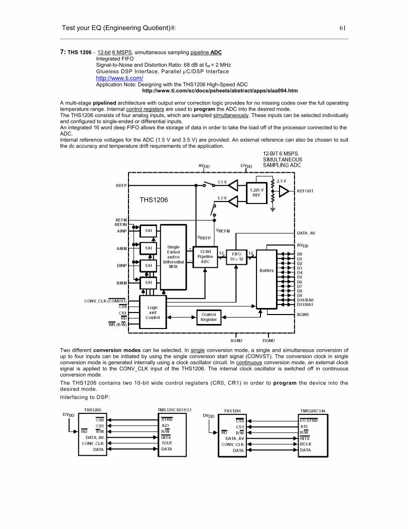
Test your EQ (Engineering Quotient)® 61 ______________________________________________________________________________________
7: THS 1206 − 12-bit 6 MSPS, simultaneous sampling pipeline ADC Integrated FIFO Signal-to-Noise and Distortion Ratio: 68 dB at fIN = 2 MHz Glueless DSP Interface, Parallel µC/DSP Interface http://www.ti.com/ Application Note: Designing with the THS1206 High-Speed ADC
http://www.ti.com/sc/docs/psheets/abstract/apps/slaa094.htm A multi-stage pipelined architecture with output error correction logic provides for no missing codes over the full operating temperature range. Internal control registers are used to program the ADC into the desired mode. The THS1206 consists of four analog inputs, which are sampled simultaneously. These inputs can be selected individually and configured to single-ended or differential inputs. An integrated 16 word deep FIFO allows the storage of data in order to take the load off of the processor connected to the ADC. Internal reference voltages for the ADC (1.5 V and 3.5 V) are provided. An external reference can also be chosen to suit the dc accuracy and temperature drift requirements of the application.
THS1206
Two different conversion modes can be selected. In single conversion mode, a single and simultaneous conversion of up to four inputs can be initiated by using the single conversion start signal (CONVST). The conversion clock in single conversion mode is generated internally using a clock oscillator circuit. In continuous conversion mode, an external clock signal is applied to the CONV_CLK input of the THS1206. The internal clock oscillator is switched off in continuous conversion mode. The THS1206 contains two 10-bit wide control registers (CR0, CR1) in order to program the device into the desired mode. Interfacing to DSP:

62 ADATKONVERTEREK ______________________________________________________________________________________
8: AD9260 − High speed oversampling ADC w/16-bit resolution @ a 2.5 MHz word rate SNR: 88.5 dB, THD: -96 dB, SFDR: 100 dB Linear phase http://www.analog.com/
The AD926012 utilizes a new analog-to-digital converter architecture to combine sigma-delta techniques with a high-speed, pipelined A/D converter. This topology allows the AD9260 to offer the high dynamic range associated with sigma-delta converters while maintaining very wide input signal bandwidth (1.25 MHz) at a very modest 8× oversampling ratio.
Figure (on the next page) provides a simplified block diagram of the AD9260. The differential analog input is fed into a second order, multibit sigma-delta modulator. This modulator features a 5-bit flash quantizer and 5-bit feedback. In addition, a 12-bit pipelined A/D quantizes the input to the 5-bit flash to greater accuracy. A special digital modulation loop combines the output of the 12-bit pipelined A/D with the delayed output of the 5-bit flash to produce the equivalent response of a second order loop with a 12-bit quantizer and 12-bit feedback. The combination of a second order loop and multibit feedback provides inherent stability: the AD9260 is not prone to idle tones or full-scale idiosyncracies sometimes associated with higher order single bit sigma-delta modulators. The output of this 12-bit modulator is fed into the digital decimation filter. The user may bring the data out undecimated (at the clock rate), or at a decimation factor of 2×, 4×, or a full 8×. The spectra of the undecimated output clearly shows the second order shaping characteristic of the quantization noise as it rises at frequencies above 1.25 MHz. The on-chip decimation filter provides excellent stopband rejection to suppress any stray input signal between 1.25 MHz and 18.75 MHz, substantially easing the requirements on any antialiasing filter for the analog input path. The decimation filters are integrated with symmetric FIR filter structures, providing a linear phase response and excellent passband flatness.
12 T. Brooks et al:
"A Cascaded Sigma-Delta Pipeline A/D converter with 1.25 MHz Signal Bandwidth and 89 dB SNR," IEEE Trans. on Solid-State Circuits, vol. 32, No. 12, pp. 1896-1905, Dec. 1997

Test your EQ (Engineering Quotient)® 63 ______________________________________________________________________________________
AD9260
Measured spectra for a 100KHz input signal with 8x decimation and filtering of output data: (a) shuffling disabled and (b) shuffling enabled
Measured spectra for a 100KHz input signal, bypassing the decimation filters: (a) 5-b modulator output (MOUT) and (b) digitally processed 12-b output of the combined
modulator and pipeline data (COUT)

64 ADATKONVERTEREK ______________________________________________________________________________________
9: A-to-D Converter Does Frequency Translation Design Note #259 [D. Redmayne] http://www.linear.com/ The need to characterize frequency sources, both in the laboratory and in the field, is increasingly important. The circuit in Figure 1 offers some interesting attributes in a compact and relatively inexpensive scheme. It uses an LTC1420 ADC 13 to undersample a higher frequency, driving an LTC1668 DAC 14, followed by a filter to perform a down conversion. The output of the analog filter is subsequently resampled to produce a manageable sample (process) rate for a single-chip microcontroller.
In addition to characterizing the carrier in an IF strip or the output of a local oscillator, this technique is also useful for characterizing ADCs, DACs, clock sources, signal sources or the effects of logic devices or phase-locked loops on phase noise. Frequency conversion or translation is usually performed by a diode mixer or a Gilbert cell mixer. Down conversion is most often encountered in radio receivers; up conversion is more commonly used in transmitters. The common superheterodyne receiver usually involves one conversion to produce a fixed intermediate frequency (IF). Spectrum analyzers, cellular base stations, cable modems, microwave and satellite receivers, radar and optical communications systems all include frequency conversion blocks.
Down Conversion with an ADC It may not be commonly known that down conversion can be performed using an ADC, by undersampling a signal frequency. The resulting output signal frequency is the difference between the sample frequency (fS) (or a multiple of fS) and the incoming frequency. An ADC may be used to undersample any frequency that is within its full linear bandwidth.
As in the case of a mixer, the result of this operation is a sum and a difference frequency. The sum frequency, however, ends up at the same apparent frequency as the difference frequency in a discrete time sampled system. Essentially, only the difference frequency remains. The major constraint in an undersampled system is that the bandwidth of the incoming signals must not fall outside the Nyquist zone in use. (A Nyquist zone extends over a bandwidth of fS/2, above or below an integral multiple of the sample frequency.) Any signal falling outside the desired Nyquist zone wraps back into the DC-to-fS/2 zone. The above constraint can be relaxed if subsequent bandpass filtering in the digital domain limits the frequency range of interest. So long as an unwanted signal does not wrap back into the frequency range of interest, its effect on the spectrum of interest is negligible.
In Figure 1, the 10Msps LTC1420 translates the 40.455MHz input signal to 455kHz at its output. When a high speed DAC is used to reproduce the 455kHz signal, a subsequent analog bandpass filter adds little cost or power dissipation. One advantage of the analog filter is that it does not exhibit mathematical artifacts if the signal frequency is not coherent with the sample rate. In fact, this scheme allows the intermediate frequency to be tailored to suit the conversion rate of the resampling LTC1417 ADC15.
analog filter
update rate resample
ratesample rate
Figure 1. Undersampling 40MHz Performs 2-Stage Frequency Translation to 100Hz
An incentive for using a high speed infinite sample-and-hold in this fashion is the benefit of a high sample rate, without the need to process samples at that rate. The data rate delivered by a high speed ADC can be too fast for a low power processor to handle and data rate decimation may reduce SNR too much.
13 12 bit, 10 MSPS pipeline ADC 14 16 bit, 50 MSPS current-steering DAC 15 14 bit, 400 KSPS charge redistribution SAR ADC

Test your EQ (Engineering Quotient)® 65 ______________________________________________________________________________________
The use of an analog filter after the DAC may seem old fashioned, but the filter characteristics available from ceramic resonators, active filters or tuned LC filters may be hard to match in a digital filter. The use of a higher resolution ADC (LTC1417) following the initial 12-bit quantization allows details to be resolved if the original signal contains a few LSB of noise (dither), as well as improving frequency measurement capability. The 455kHz intermediate signal was chosen to allow the use of readily available 455kHz ceramic resonators or LC filters. (Note that the LTC1560-1 monolithic 5th order elliptic lowpass filter could also be used in this application.) The LTC1668 DAC, as it is a current output device, can drive a tank circuit tuned to the desired frequency. The subsequent resampling of this signal at a submultiple of 455KHz – 100Hz (45,490sps) produces a sinusoid at 100Hz (!!). In Figure 2, the resampled output of the DAC is shown. Figure 3 is the result of an FFT performed on of the output of the LTC1417 ADC.
Figure 2. The Downconverted 100Hz Output Exagerates Figure 3. The Spectrum of the 100Hz Signal Phase or Frequency Variation in Original Signal Can be Processed to Determine Characteristics of the Original Signal As mentioned earlier, the output of the DAC is not only the difference frequency of 455kHz. The DAC acts like a mixer and produces in addition to the fundamental (455kHz), the sum and the difference frequencies of the 10MHz conversion clock and the 455kHz signal. The lower of these unwanted frequencies, 9.545MHz (10MHz – 455kHz), is approximately 20 times the 455kHz or 4.4 octaves above the carrier. The signal level in these components without filtering is approximately 25dB below the carrier; hence, a lowpass or bandpass filter is required. A 2nd order LPF with a 12dB/octave roll-off in the transition region will reduce these unwanted components to approximately 77dB below the carrier, the region of other harmonic and noise components. If the signal under scrutiny is a single tone, a lowpass filter is adequate. These techniques can also be used on the bench to evaluate the performance of signal generators and clock sources and of course, ADCs and DACs, as well as performing monitoring functions in the field.
Note: Serial Data Output During a Conversion (LTC1417 SAR ADC) Figure 4 shows data from the previous conversion being clocked out during the conversion with the LTC1417 ADC internal clock providing both the conversion clock and the SCLK. The internal clock has been optimized for the fastest conversion time; consequently, this mode can provide the best overall speed performance.
Figure 4. Internal Conversion Clock Selected. Data Transferred During Conversion Using the ADC Clock Output as a Master Shift Clock (SCLK Driven from CLKOUT)

66 ADATKONVERTEREK ______________________________________________________________________________________
10: A (N =)14-bit, (fN =)10 MSPS DAC Using Multi-bit Delta-Sigma Modulation System diagram:
M = 12 L = 4 K (= n) = 6
The modulator was overdesigned so that overall performance of system would be limited only the nonidealities in the analog circuits. Since 2’s complement arithmetic is used in this design, the quantizer is implemented by simply truncating the 20-bit output of the fourth integrator stage to its six most significant bits. All multiplier coefficient are designed to be factors of 2. Pipelining were used to reduce the design compexity and power dissipation.
a typical example

Test your EQ (Engineering Quotient)® 67 ______________________________________________________________________________________
Figure shows the setup used for testing the prototype. An HP8131 pulse generator was used to generate the system clock. The oversampled digital input is generated by an HP16522A pattern generator, eliminating the need for the interpolation stage. The 6-bit output of the digital modulator is converted into a thermometer code that drives 63 identical current cells (continuously calibrated to a reference current). Differential-to-single-ended conversion of the analog output was performed using a low-distortion transformer, and the resulting signal was characterized using an HP3585A spectrum analyzer. The 6-bit digital output of the modulator was also driven off-chip and acquired with an HP16500C logic analyzer to verify the functionality of the digital section independent of the analog circuitry.
Special care was taken in the test setup to minimize the coupling of digital switching noise into the analog output. The clock input to the chip is a low-swing differential signal. Figure shows the measured signal-to-noise ratio (SNR) and signal-to-(noise distortion) ratio (SNDR) as functions of the input signal level for a 1-MHz digital input sine wave sampled at 120 MHz. The noise and distortion components were measured over a 5-MHz bandwidth, corresponding to a 10-MHz Nyquist rate. A frequency of 1 MHz was chosen for the signal, so that the low-order harmonic distortion components fall into the 5-MHz baseband and are included in the SNDR measurements. These measurements demonstrate 85-dB dynamic range and 80-dB peak SNDR. The harmonic distortion is dominated by the second harmonic at -83 dB for the full-scale fundamental. The second harmonic is attributed to the nonlinearity in the measurement equipment.