Adaptive Digital Predistortion with Applications for LMDS ... · Adaptive Digital Predistortion...
98
Adaptive Digital Predistortion with Applications for LMDS Systems by Daniel Eric Johnson Thesis submitted to the Faculty of the Virginia Polytechnic Institute and State University in partial fulfillment of the requirements for the degree of Master of Science in Electrical Engineering Charles W. Bostian, Chair Jeffery H. Reed Dennis G. Sweeney August 25, 2000 Blacksburg, VA Keywords: Measurement, Simulation, Nonlinear Amplification, AM-AM, AM-PM, Broadband Copyright © 2000, Daniel Eric Johnson
Transcript of Adaptive Digital Predistortion with Applications for LMDS ... · Adaptive Digital Predistortion...
Adaptive Digital Predistortion with Applications for LMDS Systems
by Daniel Eric Johnson
Thesis submitted to the Faculty of the Virginia Polytechnic Institute and State University
in partial fulfillment of the requirements for the degree of
Master of Science in
Electrical Engineering
Charles W. Bostian, Chair Jeffery H. Reed
Dennis G. Sweeney
August 25, 2000 Blacksburg, VA
Keywords: Measurement, Simulation, Nonlinear Amplification, AM-AM, AM-PM, Broadband
Copyright © 2000, Daniel Eric Johnson

Adaptive Digital Predistortion with Applications for LMDS Systems
Daniel Eric Johnson
(ABSTRACT)
A limiting factor in the widespread deployment of LMDS systems is the limited distance of current systems. Rain attenuation and limited transmitter power are the primary causes of the limited distance. Adaptive digital predistortion is presented as a method of increasing effective transmitter power.
A background on LMDS link design, non-linear amplification, and predistortion is presented to assist the reader. A developed simulation uses AM-AM and AM-PM characteristics obtained from laboratory measurements of a 28 GHz amplifier to determine the effect of several predistortion implementation options and to confirm the feasibility of the proposed architecture.
The potential impact of this predistortion architecture on LMDS system design is considered. The presented multi-stage predistortion architecture is found to be capable of implementation at Msymbol/second rates utilizing a FPGA or custom IC and a moderate speed digital signal processor.

iii
Acknowledgements
I would like to thank Dr. Bostian for being my advisor throughout my graduate school
career. His experience with advising students made my stay enjoyable, and his
comments and suggestions greatly improved this thesis. I am grateful that he is an
advisor that always provided options rather than decisions. I would also like to thank my
other committee members. Dr. Sweeney provided invaluable assistance in performing
the amplifier measurements. Dr. Reed exposed me to the topic of adaptive digital
predistortion during his class and suggested the topic during the initial phases of my
research.
I would like to thank Dr. Sanjay Raman for use of the network analyzer and Chris
Haskins for his assistance with the operation and setup of the network analyzer. Barry
Taylor of Agilent Technologies provided the millimeter-wave amplifiers for
measurement. The measurements would not have been possible without these people.
I would also like to thank CWT, Virginia Tech’s Communication Network Services, and
WavTrace for their financial support and opportunities during my stay at Virginia Tech.
I would like to thank the faculty, staff, and students of CWT for their assistance during
my stay at Virginia Tech. I am grateful to Cortney Martin, John Nichols, and Tim
Callahan and the many other people at CNS for their assistance and friendship.
Finally, I would like to thank my friends and family that supported my decision to return
to graduate school.

iv
Table of Contents
CHAPTER 1. INTRODUCTION .........................................................................1
CHAPTER 2. THEORY...................................................................................... 3
2.1 Link Margin........................................................................................................... 3 2.1.1 Introduction.....................................................................................................3 2.1.2 Percent Reliability...........................................................................................3 2.1.3 Clear Weather Margin.....................................................................................3 2.1.4 Receiver Sensitivity.........................................................................................3 2.1.5 Antenna Gain vs. Beamwidth..........................................................................4 2.1.6 Free Space Loss...............................................................................................6 2.1.7 Rain Attenuation.............................................................................................7 2.1.8 Maximum Link Distance.................................................................................8
2.2 Amplifier Theory................................................................................................. 10 2.2.1 Non-linear Effects of Typical Power Amplifier............................................10 2.2.2 Amplifier Class.............................................................................................11 2.2.3 Backoff..........................................................................................................13 2.2.4 Traditional Amplifier Characterizations.......................................................13 2.2.5 Distortion Characterizations..........................................................................14
2.3 Predistortion Theory........................................................................................... 19 2.3.1 Advantages of Linearization.........................................................................19 2.3.2 Linearization Techniques..............................................................................19 2.3.3 Adaptive Digital Predistortion......................................................................22
CHAPTER 3. MEASUREMENT.......................................................................30
3.1 Measurement Motivation ................................................................................... 30
3.2 Measurement Procedure..................................................................................... 30
3.3 Measurement Results.......................................................................................... 36 3.3.1 Fixed 30 dB Attenuator.................................................................................37 3.3.2 HMMC-5040 Amplifier................................................................................39 3.3.3 Combined Amplifier Reference....................................................................41 3.3.4 Combined Amplifier at Different Frequencies..............................................43 3.3.5 Combined Amplifier with Low Drain Voltage.............................................44 3.3.6 Combined Amplifier with Low Drain Current..............................................46 3.3.7 Combined Amplifier with Reduced Temperature.........................................48
CHAPTER 4. SIMULATION ............................................................................51
v
4.1 Simulation Overview........................................................................................... 51
4.2 Simulation Design................................................................................................ 52 4.2.1 Transmitter....................................................................................................52 4.2.2 Receiver.........................................................................................................60
4.3 Simulation Results............................................................................................... 62 4.3.1 Peak-to-Average Ratio..................................................................................62 4.3.2 Polynomial Order..........................................................................................65 4.3.3 Forward Table Size.......................................................................................68 4.3.4 Dispersion Due to Filtering...........................................................................69 4.3.5 Optimum Amplifier Input Power..................................................................70 4.3.6 Adjacent Channel Power Ratio.....................................................................72 4.3.7 Computation Complexity..............................................................................74 4.3.8 Maladjusted Predistorter...............................................................................74
CHAPTER 5. APPLICATIONS TO LMDS....................................................... 77
5.1 Proposed Multi-stage Implementation for LMDS ........................................... 77 5.1.1 Quadrature Downconversion.........................................................................78 5.1.2 Forward Table...............................................................................................79 5.1.3 Digital Signal Processor................................................................................79 5.1.4 Polynomial Gain Predistorter........................................................................81 5.1.5 Required Adaptation Rate.............................................................................83
5.2 Implications of Predistortion for LMDS........................................................... 83
5.3 Conclusions .......................................................................................................... 86 5.3.1 Future Work..................................................................................................87
vi
Table of Figures
Figure 2.1: Free Space Loss vs. Distance for a 28 GHz Signal for Distances Typical in a LMDS System.............................................................................................................7
Figure 2.2: Link Outage Probability vs. Distance for a Sample LMDS System................9 Figure 2.3: Example of Crossover Distortion and Clipping..............................................12 Figure 2.4: Intermodulation, Compression, and Saturation Points...................................14 Figure 2.5: Simulated 16-QAM constellation with AM-AM distortion...........................16 Figure 2.6: Simulated 16-QAM spectrum with AM-AM distortion.................................16 Figure 2.7: Simulated 16-QAM constellation with AM-AM and AM-PM distortion......17 Figure 2.8: Simulated 16-QAM spectrum with AM-AM and AM-PM distortion............18 Figure 2.9 Feedforward Transmitter [16]..........................................................................20 Figure 2.10 Cartesian Loop Feedback [16].......................................................................21 Figure 2.11 LINC Transmitter [16]...................................................................................22 Figure 2.12: Block Diagram for a Inverse Modeling Adaptive Digital Predistortion
System [19]...............................................................................................................23 Figure 2.13: Block Diagram for a Multi-stage Predistortion System [19]........................27 Figure 3.1 Amplifier Test Configuration..........................................................................31 Figure 3.2 Amplifier under Test with Attenuator and Joining Adapter............................32 Figure 3.3 Agilent 8510C Measurement System..............................................................32 Figure 3.4 Amplifiers on Peltier Devices while Testing...................................................36 Figure 3.5 30 dB Fixed Attenuator Frequency Sweep S21 Magnitude............................37 Figure 3.6 30 dB Fixed Attenuator Power Sweep S21 Magnitude...................................38 Figure 3.7 30 dB Fixed Attenuator Power Sweep S21 Phase...........................................38 Figure 3.8 HMMC-5040 Frequency Swept S21...............................................................39 Figure 3.9 HMMC-5040 Power Swept S21 Magnitude....................................................40 Figure 3.10 HMMC-5040 Power Swept S21 Phase..........................................................40 Figure 3.11 Combined Amplifier Frequency Swept S21 Magnitude................................41 Figure 3.12 Combined Amplifier Power Swept S21 Magnitude......................................42 Figure 3.13 Combined Amplifer Power Swept S21 Phase...............................................42 Figure 3.14 Combined Amplifier Power Swept at Different Frequencies S21 Magnitude
...................................................................................................................................43 Figure 3.15 Combined Amplifier Power Swept at Different Frequencies S21 Phase......44 Figure 3.16 Low Drain Voltage Frequency Swept S21 Magnitude..................................45 Figure 3.17 Low Drain Voltage Power Swept S21 Magnitude.........................................45 Figure 3.18 Low Drain Voltage Power Swept S21 Phase.................................................46 Figure 3.19 Low Drain Current Frequency Swept S21 Magnitude..................................47 Figure 3.20 Low Drain Current Power Swept S21 Magnitude.........................................47 Figure 3.21 Low Drain Current Power Swept S21 Phase.................................................48 Figure 3.22 Reduced Temperature Frequency Swept S21 Magnitude..............................49 Figure 3.23 Reduced Temperature Power Swept S21 Magnitude....................................50 Figure 3.24 Reduced Temperature Power Swept S21 Phase............................................50 Figure 4.1 Block Diagram of Predistortion Simulator......................................................51 Figure 4.2 QPSK Constellation.........................................................................................53
vii
Figure 4.3 16-QAM Constellation....................................................................................53 Figure 4.4 64-QAM Constellation....................................................................................54 Figure 4.5 256-QAM Constellation..................................................................................54 Figure 4.6 Root-Raise Cosine Impulse Response for r=0.5 and r=0.15...........................55 Figure 4.7 Comparison of Root-Raised Cosine Filter and Raised Cosine Filter..............56 Figure 4.8 Peak Output Power Relative to Peak Input Power vs. Rolloff Factor for a
Root-Cosine Filter.....................................................................................................64 Figure 4.9 Peak-to-Average Power Ratio vs. Root-Cosine Filter Rolloff Factor.............64 Figure 4.10 Predistorter Output Magnitude vs. Input Magnitude for 8th Order Polynomial
...................................................................................................................................66 Figure 4.11 Predistorter Output Phase Shift vs. Input Magnitude for 8th Order Polynomial
...................................................................................................................................67 Figure 4.12 Real Part (FI) of Predistorter Multiplier vs. Input Power for 8th Order
Polynomial................................................................................................................67 Figure 4.13 Imaginary Part (FQ) of Predistorter Multiplier vs. Input Power for 8th Order
Polynomial................................................................................................................68 Figure 4.14 16-QAM Constellation before Non-Linear Distortion..................................69 Figure 4.15 16-QAM Constellation after Non-Linear Distortion.....................................70 Figure 4.16 EVM for 16-QAM with and without Predistortion for Various Constant
Noise Levels..............................................................................................................71 Figure 4.17 Power Spectral Density Plot with Adjustable Gain Block = 0 dB................73 Figure 4.18 Power Spectral Density Plot with Adjustable Gain Block = 6 dB................73 Figure 4.19 Maladjusted Predistorter for Different Frequencies......................................75 Figure 4.20 Maladjusted Predistorter for Different Bias...................................................75 Figure 4.21 Maladjusted Predistorter for Different Temperature.....................................76 Figure 5.1 Proposed Multi-stage Predistortion System for LMDS...................................77 Figure 5.2 Multiplier Portion of the Gain Predistorter Implementation [34]....................82 Figure 5.3 Nested Polynomial Implementation [34].........................................................82 Figure 5.4 Distance vs. Outage Probability for a 5 dB Increase in Transmitter Power....85 Figure 5.5 Distance vs. Outage Probability for a 10 dB Increase in Transmitter Power..85

1
Chapter 1. Introduction A limiting factor of current LMDS systems is the restricted distance over which they can
operate reliably. Increasing the output power of the transmit amplifier can increase the
range or reliability, but the cost per dBm increases greatly after the output power exceeds
what is possible with a single solid-state device.
The current limit for a single semiconductor device operating at 28 GHz is approximately
30 dBm. Increasing the amplifier power above this limit requires combining multiple
semiconductor devices or using vacuum tube in place of a solid-state device. Both
options are expensive and greatly increase the cost per dBm.
This high cost motivates the LMDS equipment designer to find ways to increase the
performance of the system without requiring a higher power amplifier. Two possibilities
are increasing the antenna gain or implementing predistortion.
Typical LMDS systems use QAM (Quadrature Amplitude Modulation), which is
sensitive to non-linear distortions. QAM is sensitive to non-linear distortions because the
signal has a non-constant envelope power. As the number of symbols increases, the
sensitivity to the distortion also increases because the symbols become more like each
other. The multiple amplitude nature of QAM allows it to achieve excellent bandwidth
efficiency but makes QAM susceptible to non-linear distortions.
The amplifier might capable of producing signals at higher powers, but the distortions
become more severe at higher powers. If a predistorter adapts to be the inverse of the
amplifier distortion function, the amplifier can become an ideal limiting amplifier.
Previous implementations of predistortion are for low bit rate (2400 bps) systems.
LMDS presents the challenge of having symbol rates of near 10 Msymbols/second. The
proposed mixture of digital logic and a digital signal processor is capable of achieving
predistortion at mega-symbol per second speeds.
Chapter 2 details background on link design for LMDS systems, non-linear amplifiers,
and predistortion concepts. Chapter 3 details the results and procedure used to measure a

2
28 GHz amplifier for several different operating conditions. A simulation of a digital
communications system in Chapter 4 uses these measurements in a non-linear amplifier
model. The major contributions of Chapter 4 are a determination of potential gain from
implementing predistortion with the measured amplifier and the effect of various
parameters. Chapter 5 details a proposed predistortion system suitable for operation near
10 Msymbols per second and the implications of predistortion for LMDS system design.

3
Chapter 2. Theory
2.1 Link Margin
2.1.1 Introduction
One of the most important aspects of designing a LMDS system or any other wireless
communication system is the link margin. It would not be wise to design a system that is
on the verge of failure. Therefore, all communication systems are over designed. In a
LMDS system the amount of margin or over design required is determined by the desired
link reliability.
2.1.2 Percent Reliability
LMDS links are generally designed to deliver a certain probability of outage due to rain.
This however does not take into account outages from other sources such as equipment
failure and power outages. Nevertheless, when taking into account link reliability, a
dominant cause of an outage in an LMDS link is rain attenuation.
The microwave link designer determines from customer requirements what level of
reliability is required for the link. The reliability is usually specified in a percent
availability. Some typical availability values are 99.9, 99.99%, and 99.995%. When
spoken these percent reliabilities might be called ‘three-nines’, ‘four-nines’, and ‘four-
nines and a five’ respectively. Reliability can also be specified in percent outage, which
is 100% minus the percent availability.
2.1.3 Clear Weather Margin
The clear weather margin is the amount by which the received signal strength exceeds the
receive threshold during clear weather conditions. The clear weather margin and link
distance allow the link reliability to be determined. When given the link reliability the
maximum link distance can be determined by iteration.
2.1.4 Receiver Sensitivity
This specification is needed to calculate the link margin. The receiver sensitivity is the
minimum signal required to obtain a particular bit error rate. This is usually measured for
4
a pre-FEC (pre-forward-error-correction) BER (bit error rate) of 10-6. With FEC, a near
error free link is still achievable at this BER.
Different modulations schemes require different signal to noise ratios to achieve the same
BER. For QAM (quadrature amplitude modulation) and PSK (phase shift keying) the
required signal to noise ratio for the same BER increases and the spectral efficiency
increases as the number of modulation levels increases.
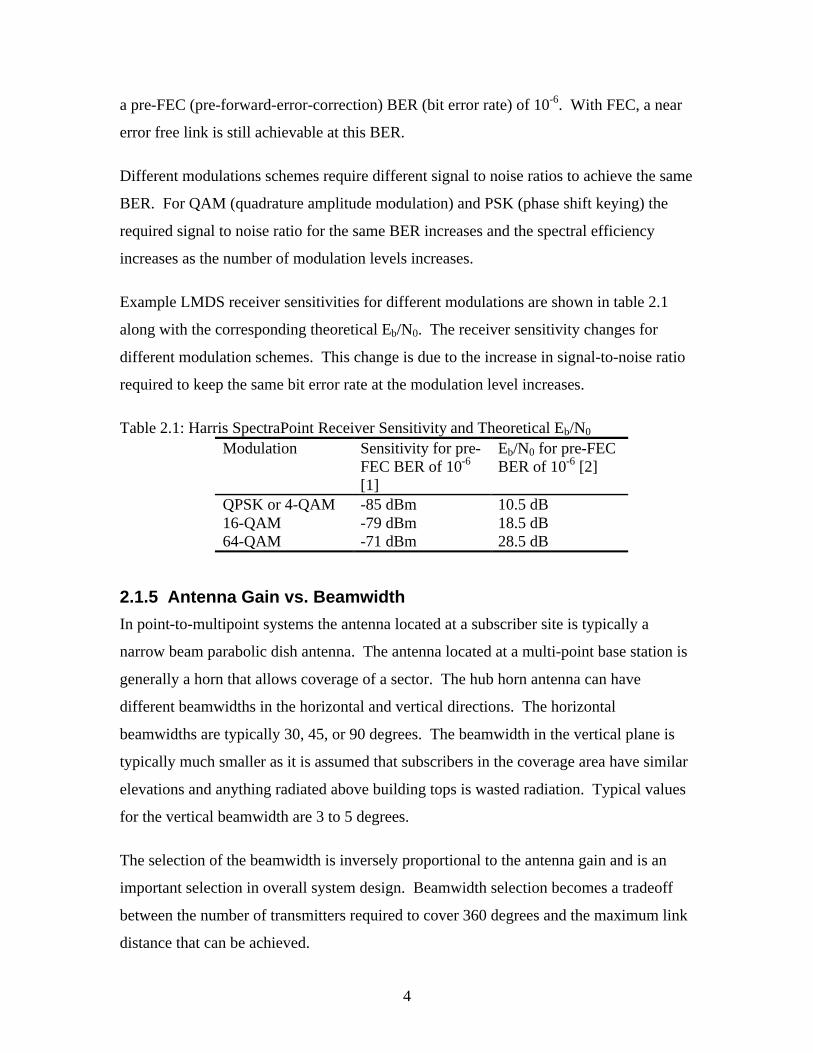
Example LMDS receiver sensitivities for different modulations are shown in table 2.1
along with the corresponding theoretical Eb/N0. The receiver sensitivity changes for
different modulation schemes. This change is due to the increase in signal-to-noise ratio
required to keep the same bit error rate at the modulation level increases.
Table 2.1: Harris SpectraPoint Receiver Sensitivity and Theoretical Eb/N0 Modulation Sensitivity for pre-
FEC BER of 10-6 [1]
Eb/N0 for pre-FEC BER of 10-6 [2]
QPSK or 4-QAM -85 dBm 10.5 dB 16-QAM -79 dBm 18.5 dB 64-QAM -71 dBm 28.5 dB
2.1.5 Antenna Gain vs. Beamwidth
In point-to-multipoint systems the antenna located at a subscriber site is typically a
narrow beam parabolic dish antenna. The antenna located at a multi-point base station is
generally a horn that allows coverage of a sector. The hub horn antenna can have
different beamwidths in the horizontal and vertical directions. The horizontal
beamwidths are typically 30, 45, or 90 degrees. The beamwidth in the vertical plane is
typically much smaller as it is assumed that subscribers in the coverage area have similar
elevations and anything radiated above building tops is wasted radiation. Typical values
for the vertical beamwidth are 3 to 5 degrees.
The selection of the beamwidth is inversely proportional to the antenna gain and is an
important selection in overall system design. Beamwidth selection becomes a tradeoff
between the number of transmitters required to cover 360 degrees and the maximum link
distance that can be achieved.

5
The vertical beamwidth geometry can limit both the maximum and minimum distances
from the transmitter. The minimum and maximum distances can be found by simple
trigonometry if the height (h) above the receiving antenna, the distance (R) from the base
station, and the vertical beamwidth (vbw) are known. The downtilt angle (t) is typically
specified as the angle below the level line to the horizon.
)tan( 21min vbwt
hR
⋅+= (Eq. 2.1)
)tan( 21max vbwt
hR
⋅−= (Eq. 2.2)
The beamwidth of the antenna is inversely related to the maximum gain of the antenna.
The beamwidth can be varied in either the horizontal or the vertical dimension and the
gain will vary inversely when either beamwidth is altered. For example, an antenna with
a 30 degree beamwidth in the horizontal plane and a 3 degree beamwidth in the vertical
plane has roughly the twice the gain when compared to an antenna with a 60 degree
beamwidth in the horizontal plane and a 3 degree beamwidth in the vertical plane.
The following equation can be used to estimate antenna gain when given the horizontal
and vertical beamwidths in degrees. The G is the antenna gain as a ratio, and the HPE°
and HPH° are the half power bandwidths of the horizontal and vertical beamwidths.
°° ⋅=
HE HPHPG
26000 (Eq. 2.3)
[4]
Using a reference horn antenna we estimate its gain. The reference antenna with a
measured gain of 22 dBi is specified to have a horizontal beamwidth of 30 degrees and a
vertical beamwidth of 3 degrees. The estimated gain using this equation results in a gain
of approximately 288.89 or 24.6 dB. It can also be seen that decreasing the beamwidth in
a single dimension increases the gain by the same factor. Using the equation again we
can find that an antenna with a 15 degree horizontal beamwidth and the same vertical
beamwidth would have a gain of approximately 27.6 dB or twice the calculated gain of

6
the reference antenna. This relationship results in a tradeoff between the antenna gain
and the number of sectors required to cover 360 degrees.
Table 2.2: Beamwidth Selection Tradeoffs Reference Beamwidth (degrees) 30 30 30 30 30 30 30 30Reference Gain (dB) 22 22 22 22 22 22 22 22Desired Beamwidth (degrees) 10 15 20 30 45 60 90 180Sectors required for full coverage 36 24 18 12 8 6 4 2Gain (dB) 26.77 25.01 23.76 22.00 20.24 18.99 17.23 14.22Change in Gain (dB) 4.77 3.01 1.76 0.00 -1.76 -3.01 -4.77 -7.78Relative number of sectors 3.00 2.00 1.50 1.00 0.67 0.50 0.33 0.17
2.1.6 Free Space Loss
As a radio signal travels through space the signal strength decreases at a rate of the square
of the increase in distance. The equation to predict the power (Pr) at the receiver is based
upon the transmitted power (Pt), wavelength of the signal (λ), distance (d) between the
transmitter and receiver, and the isotropic antenna gains of both the transmitter (Gt) and
receiver (Gr).
22
2
)4()(
d
GGPdP rtt
r πλ
= (Eq. 2.4) [2]
Since the received power and antenna gain are commonly specified in decibels, this
equation can be rearranged using logarithmic properties to the following more convenient
equation.
)(log204log20log20)( 101010)()()()( dGGPdP dBrdBtdBmtdBmr ⋅−⋅−⋅+++= πλ (Eq. 2.5)
The free space loss component of the above equation represented by the following
equation.
)(log204log20log20 101010)( dF dB ⋅−⋅−⋅= πλ (Eq. 2.6)
The figure 2.1 shows the free space loss (F) at 28 GHz for distances applicable to LMDS.

7
1000 2000 3000 4000 5000 6000 7000−140
−138
−136
−134
−132
−130
−128
−126
−124
−122
−120Free Space Loss vs Distance
Distance (meters)
Fre
e S
pace
Los
s (d
B)
Figure 2.1: Free Space Loss vs. Distance for a 28 GHz Signal for Distances Typical in a LMDS System
2.1.7 Rain Attenuation
Organizations such as the ITU publish the amount of time a year that a particular rain rate
is exceeded in a particular region [3]. This is the basis of calculating the needed margin
when given the desired reliability.
This published rain rate data can then be turned into a probability distribution function
that can show the probability of exceeding a particular rainfall rate during the entire year
at a particular location. The link should be designed with enough link margin to continue
to operate during this rain rate. The following equation can be used to calculate the
amount of attenuation for a particular distance in kilometers. The A is the attenuation per
kilometer due to rain and r is the rain rate in millimeters per hour.
βα)()(
hrmm
kmdB rA ⋅= (Eq. 2.7)
For a 30 GHz signal with horizontal polarization α = 0.187 and β=1.02.

8
Table 2.3: ITU Predicted reliability, rain rates, and attenuation for a 28 GHz signal in Blacksburg, VA
Percent Outage Percent AvailableMinutes
unavailable/yearRain rate (mm/hr)
[3]Attenuation
(dB/km)0.001 99.999 5.3 108.0 22.180.002 99.998 10.5 89.0 18.210.005 99.995 26.3 64.5 13.110.010 99.990 52.6 49.0 9.900.020 99.980 105.1 35.0 7.030.050 99.950 262.8 22.0 4.380.100 99.900 525.6 14.5 2.860.200 99.800 1051.2 9.5 1.860.500 99.500 2628.0 5.2 1.001.000 99.000 5256.0 3.0 0.572.000 98.000 10512.0 1.5 0.285.000 95.000 26280.0 0.0 0.00
Once the desired link reliability is chosen, data from rain measurements are used to
determine the corresponding rain rate that is not exceeded for the same percentage of the
time as the link reliability. This rain rate is converted into attenuation per kilometer
using equation 2.7. The attenuation per kilometer is then multiplied by the effective link
distance in kilometers to determine to attenuation due to rain at that rate. Links with a
longer distance therefore require a higher margin to operate at the same reliability. The
assumption that the effective link distance is equal to the actual link distance is used here.
This assumption is valid for short links such as those considered here.
2.1.8 Maximum Link Distance
Once the desired reliability is known, it can be converted into a minimum required
margin per kilometer. The transmitter power, receiver antenna gain, transmitter antenna
gain, and receiver sensitivity can be used to iterate the maximum distance for the link to
maintain that reliability. When rain margins are considered, the increase in radius gained
from an increase in transmitter power is not as great. This is because as the link distance
increases, the required margin also increases.
9
0 1 2 3 4 5 6 710
−3
10−2
10−1
100
Distance vs. Outage Probability
Distance (km)
Out
age
Pro
babi
lity
(%)
QPSK16−QAM64−QAM
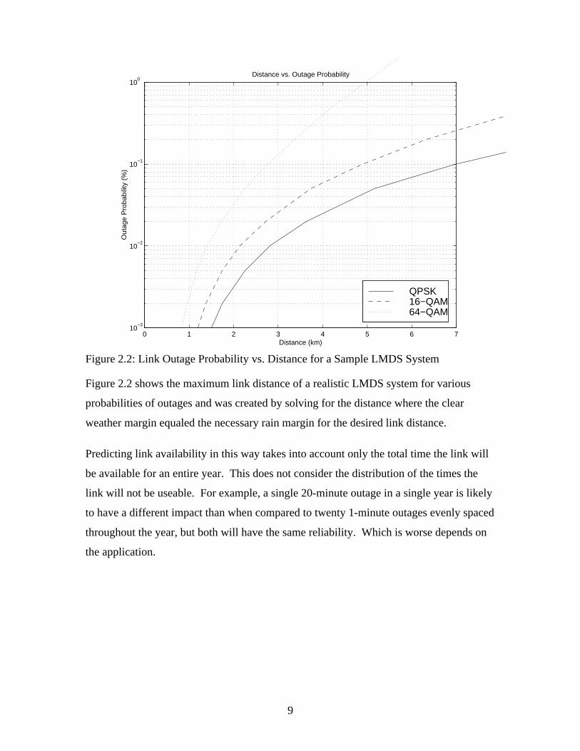
Figure 2.2: Link Outage Probability vs. Distance for a Sample LMDS System
Figure 2.2 shows the maximum link distance of a realistic LMDS system for various
probabilities of outages and was created by solving for the distance where the clear
weather margin equaled the necessary rain margin for the desired link distance.
Predicting link availability in this way takes into account only the total time the link will
be available for an entire year. This does not consider the distribution of the times the
link will not be useable. For example, a single 20-minute outage in a single year is likely
to have a different impact than when compared to twenty 1-minute outages evenly spaced
throughout the year, but both will have the same reliability. Which is worse depends on
the application.
10
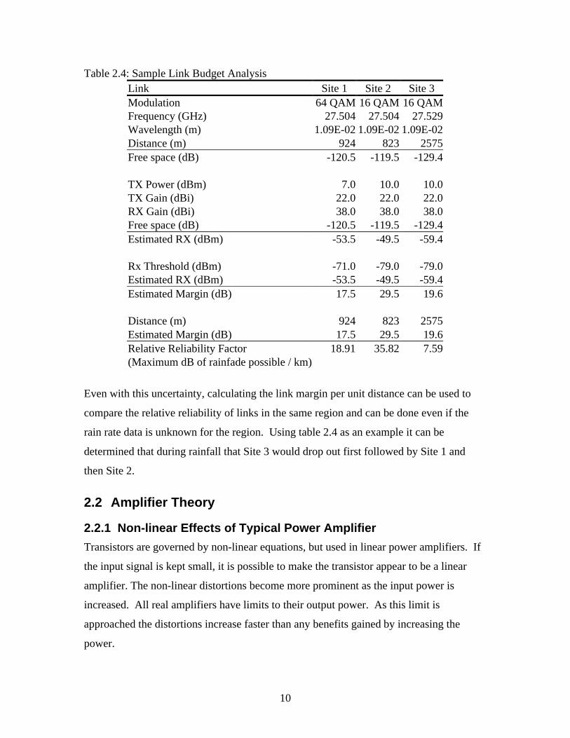
Table 2.4: Sample Link Budget Analysis Link Site 1 Site 2 Site 3 Modulation 64 QAM 16 QAM 16 QAM Frequency (GHz) 27.504 27.504 27.529 Wavelength (m) 1.09E-02 1.09E-02 1.09E-02 Distance (m) 924 823 2575 Free space (dB) -120.5 -119.5 -129.4 TX Power (dBm) 7.0 10.0 10.0 TX Gain (dBi) 22.0 22.0 22.0 RX Gain (dBi) 38.0 38.0 38.0 Free space (dB) -120.5 -119.5 -129.4 Estimated RX (dBm) -53.5 -49.5 -59.4 Rx Threshold (dBm) -71.0 -79.0 -79.0 Estimated RX (dBm) -53.5 -49.5 -59.4 Estimated Margin (dB) 17.5 29.5 19.6 Distance (m) 924 823 2575 Estimated Margin (dB) 17.5 29.5 19.6 Relative Reliability Factor 18.91 35.82 7.59 (Maximum dB of rainfade possible / km)
Even with this uncertainty, calculating the link margin per unit distance can be used to
compare the relative reliability of links in the same region and can be done even if the
rain rate data is unknown for the region. Using table 2.4 as an example it can be
determined that during rainfall that Site 3 would drop out first followed by Site 1 and
then Site 2.
2.2 Amplifier Theory
2.2.1 Non-linear Effects of Typical Power Amplifier
Transistors are governed by non-linear equations, but used in linear power amplifiers. If
the input signal is kept small, it is possible to make the transistor appear to be a linear
amplifier. The non-linear distortions become more prominent as the input power is
increased. All real amplifiers have limits to their output power. As this limit is
approached the distortions increase faster than any benefits gained by increasing the
power.

11
2.2.2 Amplifier Class
Amplifiers are divided into several different classes. Different classes have different bias
networks, linearity, and efficiencies. A Class A amplifier offers the most linear response
of the amplifiers considered below. However, this high linearity comes at the price of
power efficiency. The power efficiency or η can be considered to be defined by the
equation below.
)(Ppower supply
)(Ppower load�
s
L= [5] (Eq. 2.8)
The transistors in a Class A amplifier are always biased to obtain high linearity. The
theoretical maximum power efficiency of 25% is obtained when the transistor is at the
edge of saturation. The transistor shows non-linear effects before reaching the saturation
point and the practical efficiencies obtained are around 10% to 20%. [5]
The Class B amplifier trades linearity for a higher power efficiency (η) than the Class A.
The transistors are not turned on unless a signal exceeds a threshold in either the negative
or positive direction. This causes what is called crossover distortion or a ‘dead band’.
The theoretical maximum power efficiency (η) for a class B amplifier with a sinusoidal
input is 78.5%. [5]
12
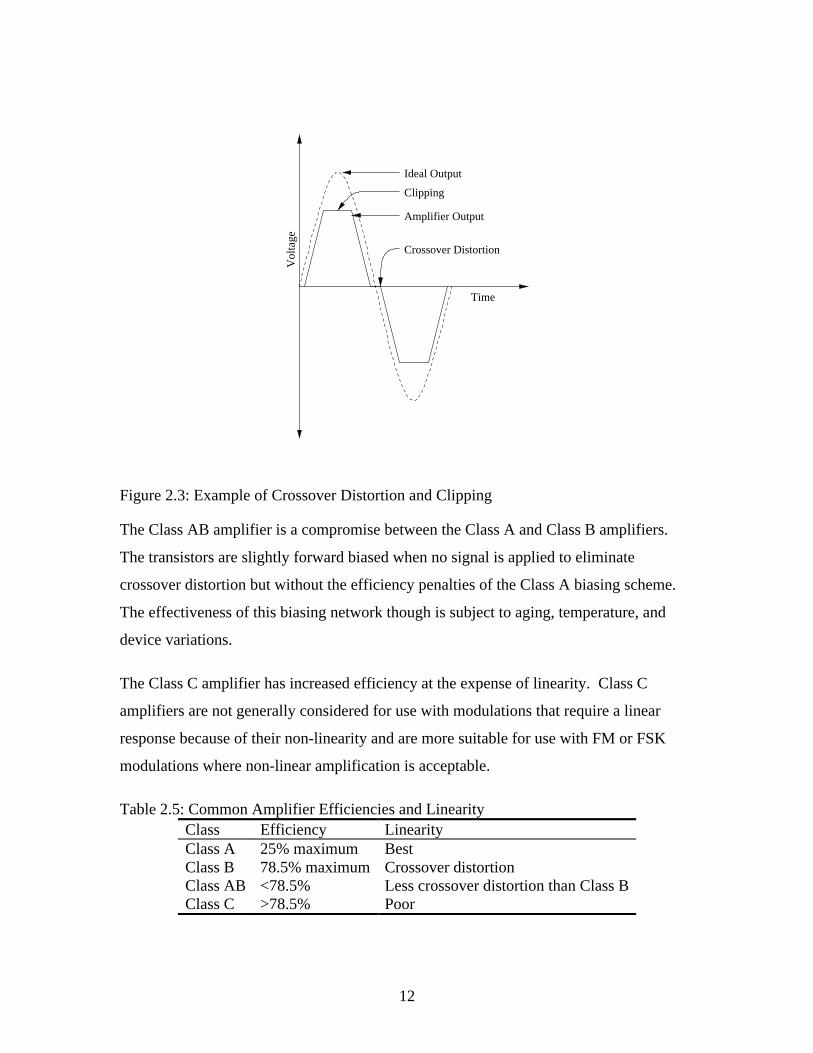
Vol
tage
Time
Crossover Distortion
Amplifier Output
Clipping
Ideal Output
Figure 2.3: Example of Crossover Distortion and Clipping
The Class AB amplifier is a compromise between the Class A and Class B amplifiers.
The transistors are slightly forward biased when no signal is applied to eliminate
crossover distortion but without the efficiency penalties of the Class A biasing scheme.
The effectiveness of this biasing network though is subject to aging, temperature, and
device variations.
The Class C amplifier has increased efficiency at the expense of linearity. Class C
amplifiers are not generally considered for use with modulations that require a linear
response because of their non-linearity and are more suitable for use with FM or FSK
modulations where non-linear amplification is acceptable.
Table 2.5: Common Amplifier Efficiencies and Linearity Class Efficiency Linearity Class A 25% maximum Best Class B 78.5% maximum Crossover distortion Class AB <78.5% Less crossover distortion than Class B Class C >78.5% Poor

13
2.2.3 Backoff
As the input power is increased, the output power approaches a maximum or saturation.
The distance in decibels between the average input power and the saturated input power
is called the ‘backoff’. As backoff is reduced, a point is reached were any additional
increase in input power does not result in improved link error performance. The location
of this point is dependent upon amplifier characteristics and the characteristics of the
modulation.
The input backoff is defined by [6] to be the ratio of the input power required to achieve
saturation to the average input power.
in
inSat
P
PIBO 10log10= [6] (Eq. 2.9)
Two things happen when the QAM modulation index increases. The transmitted signal
becomes more sensitive to distortions in the transmitter and a higher Eb/N0 is required at
the receiver to maintain the same BER performance. As a result, increasing the
modulation index will require an increase in backoff. The link margin of a higher
modulation index is therefore reduced by both the higher Eb/N0 requirement as expected
and by the decrease in average input power or increase in backoff [7].
2.2.4 Traditional Amplifier Characterizations
2.2.4.1 Third Order Intercept Point (IP3) Third order intermodulation products are of interest in characterizing amplifier
performance because third order products are very close in frequency to the desired
signal. The 3rd order intercept point is a figure of merit associated with 3rd order
intermodulation products and is the point at which third-order products overtake the
desired first order component. The IP3 can be specified by either the input power at
which the 3rd order products equal the desired signal or the output power at which the 3rd
order products are equal to the desired signal. It is possible that this point is beyond the
maximum output power of the amplifier. In this case the point is located at the
intersection of input vs. output power gain curves. If referenced from the output power
14
this is called the OIP3 and IIP3 if referenced from the input power. Intermodulation
products with odd orders such as the 3rd and 5th order products are considered because
they can create interference within the bandwidth of the desired signal. [8]
Input PowerIIP3
IP3
Out
put P
ower
Real Amplifier ResponseOIP3
1dB Compression Point
Saturation Point
1st Order Ideal Linear Response
3rd order
Figure 2.4: Intermodulation, Compression, and Saturation Points
2.2.4.2 1 dB Gain Compression Point The 1 dB compression point is defined as the point at which the output of an amplifier
has dropped 1 dB below the idea linear output. Compression points might be specified
for particular amounts of compression. Other commonly specified points are 3 dB and
0.1 dB below ideal gain. The AM-AM distortion curve can be used to determine these
points.
2.2.4.3 Saturation Point Saturation occurs when the maximum input power is exceeded. At this point the output
is ‘clipped’ to a maximum voltage, and gain compression results until a maximum power
is achieved. Saturation also causes phase modulation of the signal by the power amplifier
[9].
2.2.5 Distortion Characterizations
Additional amplifier characterizations can give a more accurate representation of non-
linear distortions in an amplifier. When a signal is sent through a near linear amplifier

15
the amplifier gain and phase shift are functions of the input amplitude. The following
equation represents the input to the amplifier where R is the amplitude of the input signal.
[ ])(cos)()( ttwtRtx xox θ+⋅= [10] (Eq. 2.10)
The output of the amplifier (y) can be expressed as the following, where G is the
amplitude distortion as a function of the input amplitude and Ψ is the phase distortion as
a function of the input amplitude Rx.
( )[ ] ( ) ( )[ ]{ }tRttwtRGty xxox Ψ++⋅= θcos)( [10] (Eq. 2.11)
Although the output is shown in a polar form here, implementations typically use I and Q
signals.
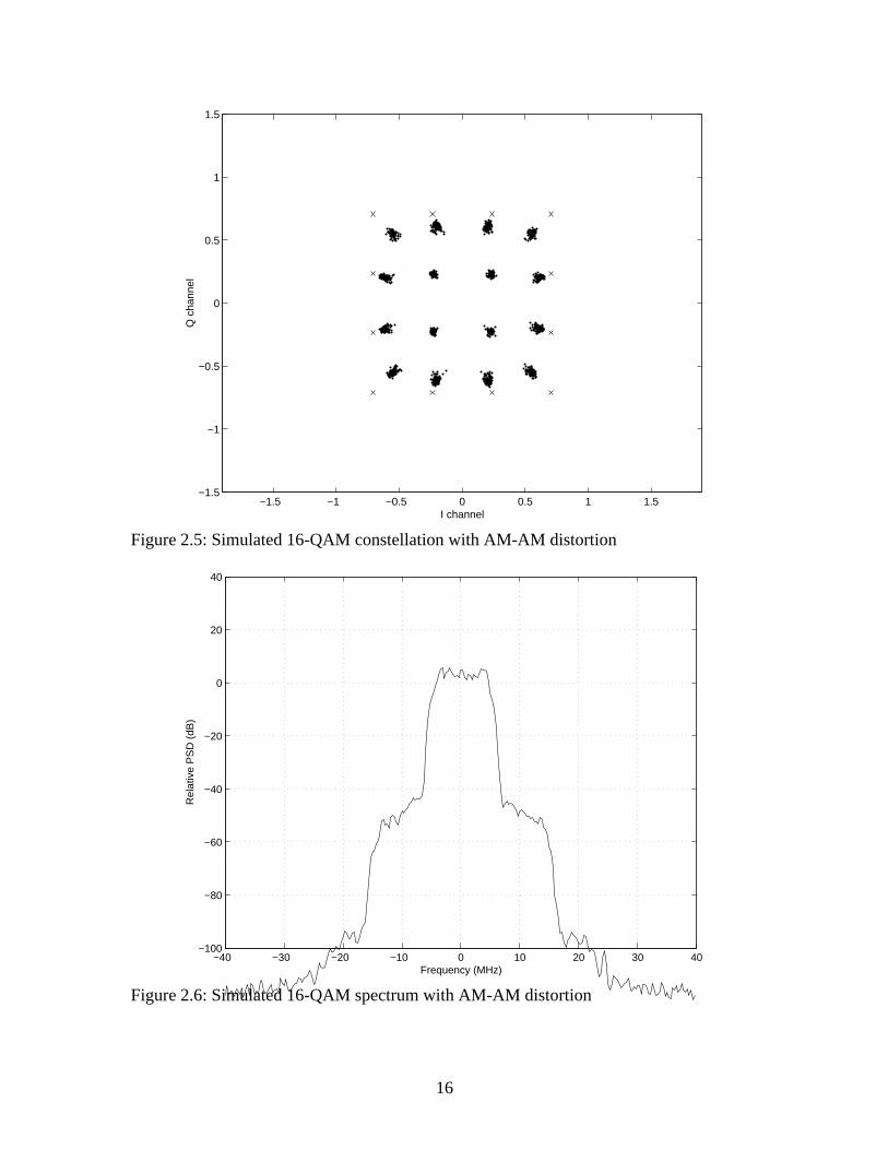
2.2.5.1 AM-AM Distortion The ideal amplifier has constant gain across all input powers. A practical amplifier has a
maximum output power, which will limit the output power to a particular value. In
reality as this limit is approached gradually as the apparent gain of an amplifier decreases
with increasing input. The AM-AM distortion is created by this variation in the gain of
the amplifier across different input powers. The AM-AM distortion graph can be used to
determine the gain compression for any input power.
16
−1.5 −1 −0.5 0 0.5 1 1.5−1.5
−1
−0.5
0
0.5
1
1.5
I channel
Q c
hann
el
Figure 2.5: Simulated 16-QAM constellation with AM-AM distortion
−40 −30 −20 −10 0 10 20 30 40−100
−80
−60
−40
−20
0
20
40
Frequency (MHz)
Rel
ativ
e P
SD
(dB
)
Figure 2.6: Simulated 16-QAM spectrum with AM-AM distortion
17
The constellation and spectrum of a severely AM-AM distorted 16-QAM signal is show
in the previous figures. The distortion gives the constellation compressed spacing at its
outer points. The dispersion in the constellation is not due to noise, as this signal
contained no noise. The dispersion is induced by the root raised cosine filter and is
described in more detail later. The ‘X’ shows the desired constellation point location.
The inner four points are dispersed around the ideal point while the outer points are being
‘compressed’ with the corner points showing the most compression.
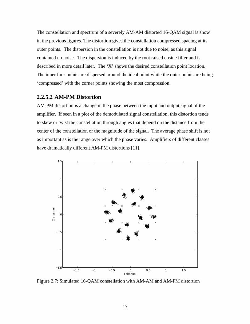
2.2.5.2 AM-PM Distortion AM-PM distortion is a change in the phase between the input and output signal of the
amplifier. If seen in a plot of the demodulated signal constellation, this distortion tends
to skew or twist the constellation through angles that depend on the distance from the
center of the constellation or the magnitude of the signal. The average phase shift is not
as important as is the range over which the phase varies. Amplifiers of different classes
have dramatically different AM-PM distortions [11].
−1.5 −1 −0.5 0 0.5 1 1.5−1.5
−1
−0.5
0
0.5
1
1.5
I channel
Q c
hann
el
Figure 2.7: Simulated 16-QAM constellation with AM-AM and AM-PM distortion
18
−40 −30 −20 −10 0 10 20 30 40−100
−80
−60
−40
−20
0
20
40
Frequency (MHz)
Rel
ativ
e P
SD
(dB
)
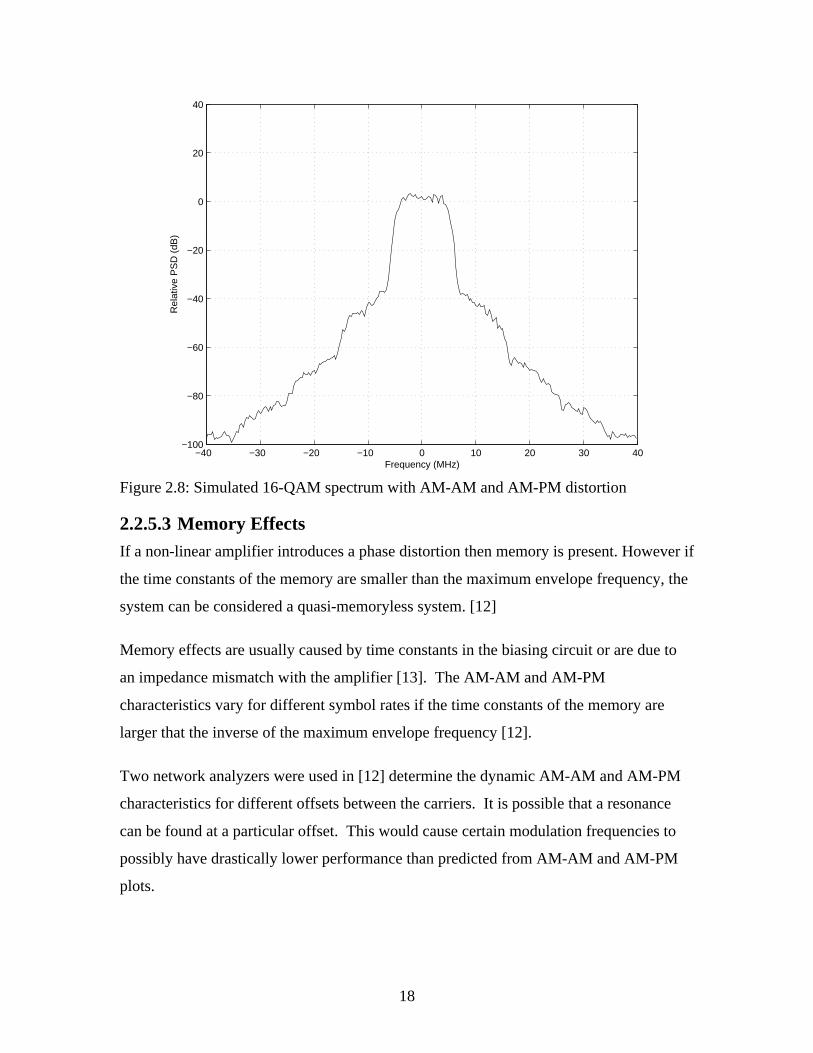
Figure 2.8: Simulated 16-QAM spectrum with AM-AM and AM-PM distortion
2.2.5.3 Memory Effects If a non-linear amplifier introduces a phase distortion then memory is present. However if
the time constants of the memory are smaller than the maximum envelope frequency, the
system can be considered a quasi-memoryless system. [12]
Memory effects are usually caused by time constants in the biasing circuit or are due to
an impedance mismatch with the amplifier [13]. The AM-AM and AM-PM
characteristics vary for different symbol rates if the time constants of the memory are
larger that the inverse of the maximum envelope frequency [12].
Two network analyzers were used in [12] determine the dynamic AM-AM and AM-PM
characteristics for different offsets between the carriers. It is possible that a resonance
can be found at a particular offset. This would cause certain modulation frequencies to
possibly have drastically lower performance than predicted from AM-AM and AM-PM
plots.
19
2.2.5.4 Adjacent Channel Power Ratio (ACPR) The adjacent channel power ration or ACPR is defined by [13] to be the power contained
within the upper and lower adjacent channels divided by the power in the main channel.
The division of the power in either the upper or lower channel by the main channel power
is represented by ACPRUPPER or ACPRLOWER. Variations in the definition are possible by
defining different frequencies for the start and stop of the adjacent channel. Other names
for ACPR include adjacent channel interference ratio (ACIR) [14] and signal to
intermodulation power ratio (SIMR) [7].
The increase in ACPR after an amplifier with non-linear effects amplifies a signal is
called spectral regrowth [13]. This increase ‘steals’ power that could otherwise be used
for the desired signal while potentially interfering with adjacent signals or inefficiently
using spectrum [15].
It is difficult to relate IP3 and ACPR because IP3 is measured with a relatively simple
two-tone measurement while ACPR is measured as a result of complex linear
modulations and cannot be represented by a finite number of tones [13].
2.3 Predistortion Theory
2.3.1 Advantages of Linearization
The advantages of amplifier linearization include a reduction in adjacent channel
interference or out-of-band distortion, a reduction of in-band distortion, and an increase
in power efficiency. Out-of band distortion is undesirable because it robs power from the
desired signal as well as interferes with the adjacent channels. A reduction of the in-band
distortion will result in an increase in effective transmitter power. Linearization can also
enable the use of less linear but more power efficient amplifiers.
2.3.2 Linearization Techniques
2.3.2.1 Addition of a Non-Linear Component For this method, a non-linear component such as a diode corrects the non-linear
characteristics of the power amplifier. The ideal diode for this purpose has near opposite
AM-AM and AM-PM characteristics of the amplifier. The method has the advantage of
20
being easy to implement but it may not completely correct the non-linear effects of the
amplifier. [16]
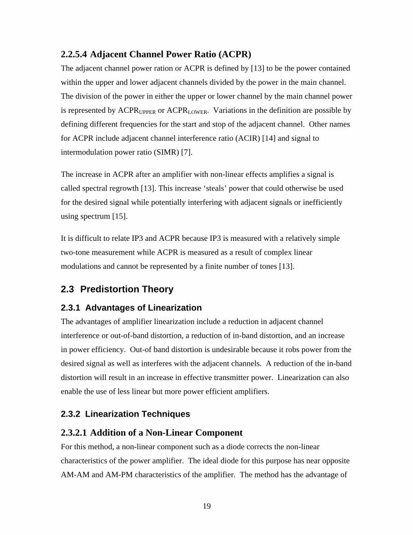
2.3.2.2 Feedforward The feedforward method generates an error signal by subtracting the signal at the input of
the amplifier from an attenuated version of the amplifier output. Analog methods are
used to amplify the error signal and subtract it from the output of the amplifier. The
result of the subtraction is the amplified desired signal. Disadvantages of this method
include requiring a powerful error-signal amplifier to cancel the distortion after the
amplifier, complexity, and adjustment.[10] Imperfections in the error-amplifier also
degrade the performance of the feedforward method. [16]
Main Amplifier
Delay Line
Attenuator
Delay Line
Error Amplifier
Error InjectionCouplerCoupler
HybridCombiner
RF Input
RF Output
++
Figure 2.9 Feedforward Transmitter [16]
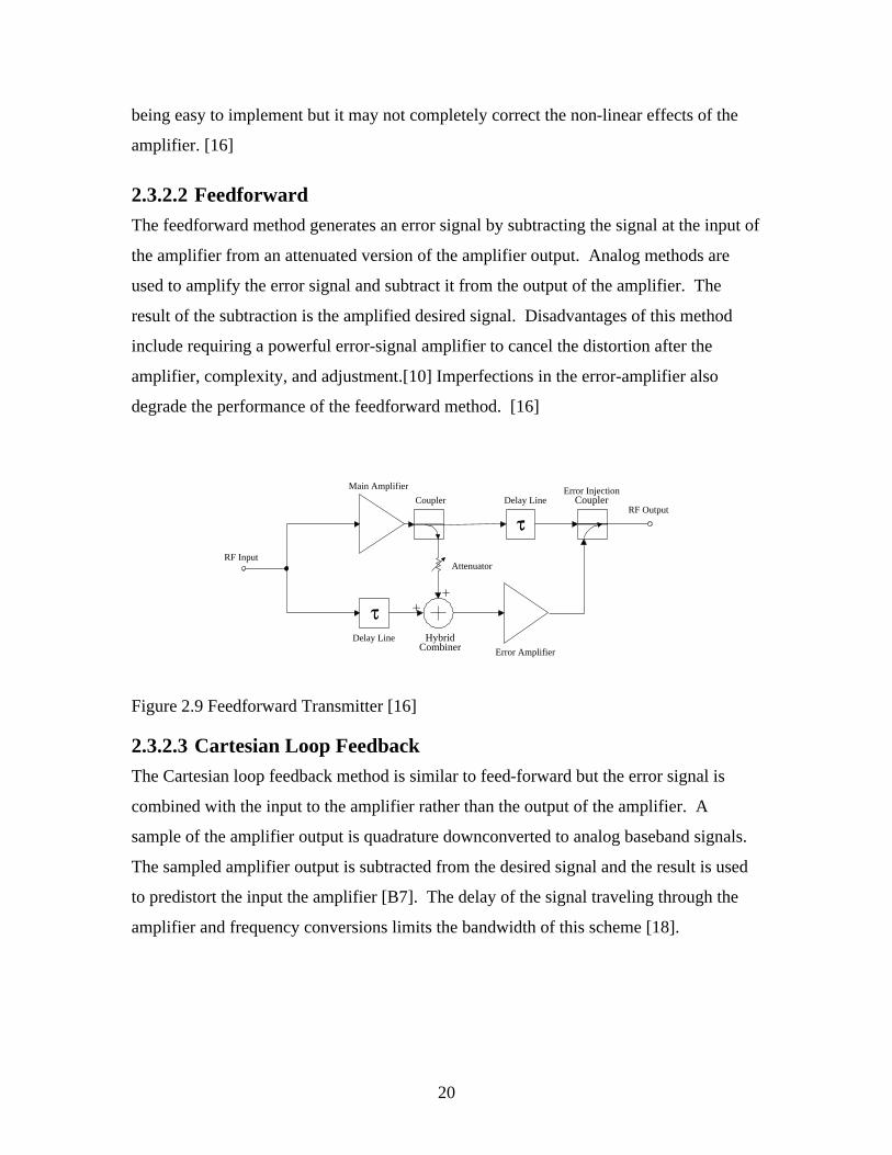
2.3.2.3 Cartesian Loop Feedback The Cartesian loop feedback method is similar to feed-forward but the error signal is
combined with the input to the amplifier rather than the output of the amplifier. A
sample of the amplifier output is quadrature downconverted to analog baseband signals.
The sampled amplifier output is subtracted from the desired signal and the result is used
to predistort the input the amplifier [B7]. The delay of the signal traveling through the
amplifier and frequency conversions limits the bandwidth of this scheme [18].
21
+
_
+
_
BasebandI
BasebandQ
90o
PA
90o
LO
LO
LPF
LPF
Figure 2.10 Cartesian Loop Feedback [16]
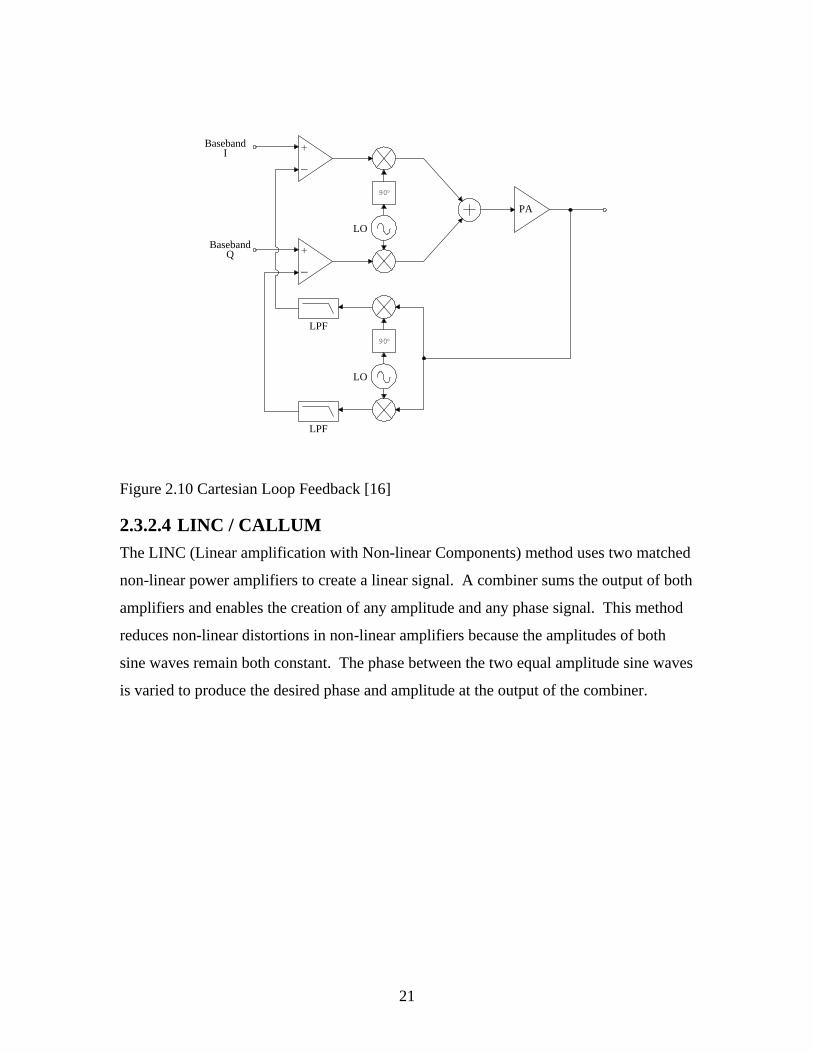
2.3.2.4 LINC / CALLUM The LINC (Linear amplification with Non-linear Components) method uses two matched
non-linear power amplifiers to create a linear signal. A combiner sums the output of both
amplifiers and enables the creation of any amplitude and any phase signal. This method
reduces non-linear distortions in non-linear amplifiers because the amplitudes of both
sine waves remain both constant. The phase between the two equal amplitude sine waves
is varied to produce the desired phase and amplitude at the output of the combiner.
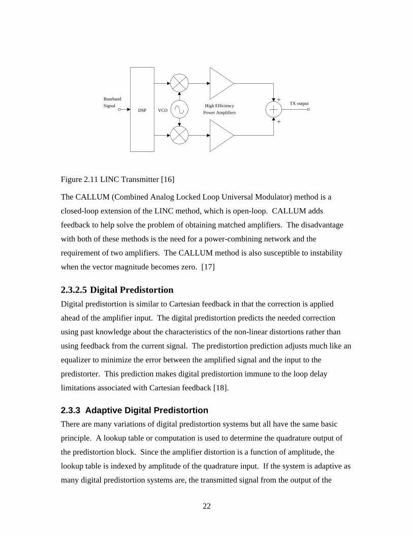
22
TX output
DSPHigh Efficiency
Power Amplifiers
Baseband
SignalVCO
+
+
Figure 2.11 LINC Transmitter [16]
The CALLUM (Combined Analog Locked Loop Universal Modulator) method is a
closed-loop extension of the LINC method, which is open-loop. CALLUM adds
feedback to help solve the problem of obtaining matched amplifiers. The disadvantage
with both of these methods is the need for a power-combining network and the
requirement of two amplifiers. The CALLUM method is also susceptible to instability
when the vector magnitude becomes zero. [17]
2.3.2.5 Digital Predistortion Digital predistortion is similar to Cartesian feedback in that the correction is applied
ahead of the amplifier input. The digital predistortion predicts the needed correction
using past knowledge about the characteristics of the non-linear distortions rather than
using feedback from the current signal. The predistortion prediction adjusts much like an
equalizer to minimize the error between the amplified signal and the input to the
predistorter. This prediction makes digital predistortion immune to the loop delay
limitations associated with Cartesian feedback [18].
2.3.3 Adaptive Digital Predistortion
There are many variations of digital predistortion systems but all have the same basic
principle. A lookup table or computation is used to determine the quadrature output of
the predistortion block. Since the amplifier distortion is a function of amplitude, the
lookup table is indexed by amplitude of the quadrature input. If the system is adaptive as
many digital predistortion systems are, the transmitted signal from the output of the
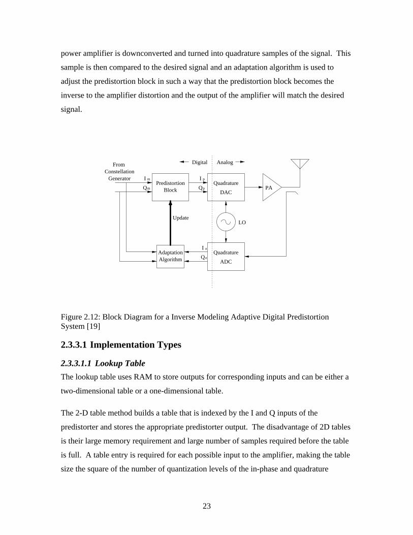
23
power amplifier is downconverted and turned into quadrature samples of the signal. This
sample is then compared to the desired signal and an adaptation algorithm is used to
adjust the predistortion block in such a way that the predistortion block becomes the
inverse to the amplifier distortion and the output of the amplifier will match the desired
signal.
Quadrature
ADCAlgorithmAdaptation
LO
Quadrature
DAC
From
PAPredistortion
Block
Q
I
I
Q
Update
I
Qm p
m p
ConstellationGenerator
a
a
AnalogDigital
Figure 2.12: Block Diagram for a Inverse Modeling Adaptive Digital Predistortion System [19]
2.3.3.1 Implementation Types
2.3.3.1.1 Lookup Table
The lookup table uses RAM to store outputs for corresponding inputs and can be either a
two-dimensional table or a one-dimensional table.
The 2-D table method builds a table that is indexed by the I and Q inputs of the
predistorter and stores the appropriate predistorter output. The disadvantage of 2D tables
is their large memory requirement and large number of samples required before the table
is full. A table entry is required for each possible input to the amplifier, making the table
size the square of the number of quantization levels of the in-phase and quadrature
24
samples. The advantage of the 2-D table is that no polar-to-rectangular or rectangular-to-
polar conversions are necessary.
),( mmIP QIFI = [20] (Eq. 2.12)
),( mmQP QIFQ = [20] (Eq. 2.13)
Another method uses two 1-D tables to correct for amplitude and phase distortion. The
following equations demonstrate how the 1-D polar table might be implemented. RP
represents the magnitude of the predistorter output, FR represents the AM-AM function of
the predistorter, Fφ represents the AM-PM function of the predistorter, RM represents the
magnitude of the predistorter input, φP represents the phase of the signal at the output of
the predistorter, and φM represents the phase of the signal at the input of the predistorter.
)( MRP RFR = [21] (Eq. 2.14)
)( PMP RFφφφ += [21] (Eq. 2.15)
The above equation shows the phase offset (Fφ) as a function of the output of the
predistorter (RP) rather than the input magnitude (RM). This implementation is called the
cascade implementation and has the desirable effect of separating the convergence of the
phase and magnitude characteristics [21]. Enhancements to the 1-D tables include using
interpolation methods to reduce the number of entries required. A disadvantage of the
1-D table is that it requires conversions between rectangular and polar representations.
2.3.3.1.1.1 Lookup Table Size
An implementation can have a table entry for every possible digital value. If the number
of bits used to quantize the signal is represented by n, a full two dimensional table
memory requires (2n)2 entries while a one dimensional table requires a two tables of 2n
values. The use of interpolation can be used to decrease the number of points required in
the look up table [22].
Table size has an inverse relationship with adjacent channel interference [18]. Each
doubling of the table size decreases the ACPR by 6 dB up to a limit after which
25
increasing the table size no longer reduces the adjacent channel interference. The
specific case in [22] shows a 6dB decrease in adjacent channel interference for every
doubling of the look up table size up to 256 entries using interpolation.
2.3.3.1.1.2 Table Indexing
The spacing between table entries must be considered if a table entry does not exist for
every possible quantized value. The typical options for index spacing are optimal
indexing, equal amplitude indexing, and equal power indexing. The optimal index
spacing can be found by applying a method detailed in [23] that is similar to the
Lloyd-Max algorithm for picking optimal points for quantization. This calculation
depends on amplifier distortion, the probability density function of the modulation, and
the level of backoff. [23]
The equal power spacing has the worst spacing scheme for class AB amplifiers. The
equal power spacing concentrates more points in the saturation region rather than in the
low power region where crossover distortion lies. Nevertheless, equal power indexing
has a computational advantage because the predistortion is a function of power
eliminating the requirement for calculating the square root. [23]
The equal amplitude spaced method is a compromise of simplicity and performance. The
method has intermodulation powers of 4 dB to 10 dB better than the equal power spacing
method and is 1 dB to 4 dB worse than optimal spacing. [23]
2.3.3.1.1.3 Table Load Time
[14] has derived the time required to trace every path. Where T is the total time required
to trace all paths, N is the number of symbols, W is the symbol rate, and L is number of
symbols stored in the raised-cosine filter.
W
NT
L
= [14]
(Eq. 2.16)
The time to load the table is most important in low symbol rate systems where it can take
10 seconds to trace all possible points.

26
2.3.3.1.2 Calculation
An alternative to using a lookup table is to use a computation to calculate the output
signal as a function of the input signal. This method is favorable because of the
elimination of large banks of RAM required by the table look-up method.
A polynomial function is one way to perform a calculation predistorter. As polynomial
order is increased the model becomes closer to the amplifier distortions but
computational load is increased. It was noted in [24] that a 16th order polynomial with
nine even terms was sufficient to model the AM-PM distortions. Similarly, a ninth order
polynomial with five odd terms was sufficient to model the AM-AM distortions.
2.3.3.1.2.1 Adaptation Algorithms
If a calculation such as interpolation or a polynomial is used to predistidort, then an
adaptation algorithms are necessary to adjust the function or table values that control the
predistorter. Adaptation algorithms or optimization methods are divided into two basic
categories. Direct methods provide the exact answer within a predetermined number of
calculations and are the preferred method for orders less that 100 [25]. Iteration or
gradient methods approach a solution gradually. Methods such as LMS, RLS, RASCAL
[35], Secant [11, 18] have all been proposed for optimizing predistoter functions and
lookup tables.
2.3.3.2 Multi-stage Predistortion In the multi-state predistortion proposed in [19], the forward model of the power
amplifier is determined by comparing samples from the predistorter output to the samples
downconverted and digitized from the power amplifier output. This multi-stage method
then uses the forward model to generate the inverse model needed in the predistortion
block. Synthetic data formulated to speed convergence of the model can then be used to
determine the predistorter without interrupting the data being sent by the transmitter. This
method eliminates the delays of waiting for a symbol to propagate through the analog
chain or the delay of waiting for the input sample to change. [19]
27
Quadrature
ADC
LO
Algorithm
ReverseAdaptation
ForwardModel
SimulatorGeneratorSequence
Q
I
Q
I
Block
Predistortion Quadrature
DACPA
Algorithm
ForwardAdaptation
Update
Update
m
m
a
a
I p
Qp
From Constellation
Generator
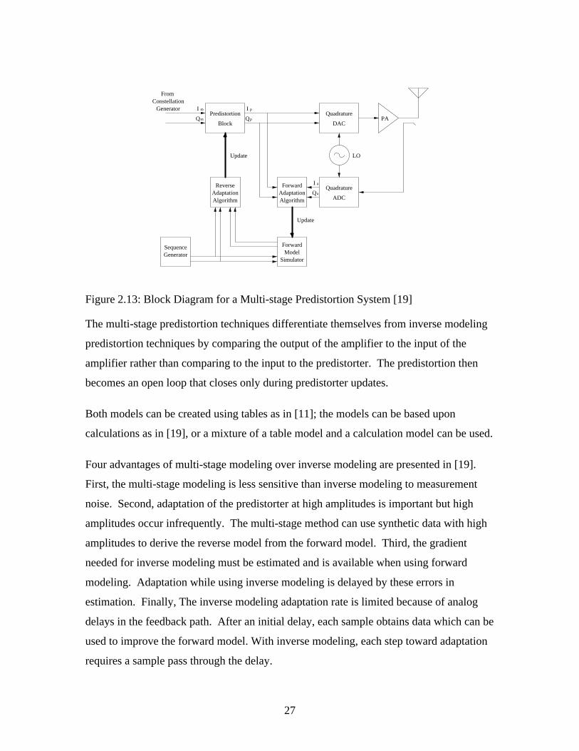
Figure 2.13: Block Diagram for a Multi-stage Predistortion System [19]
The multi-stage predistortion techniques differentiate themselves from inverse modeling
predistortion techniques by comparing the output of the amplifier to the input of the
amplifier rather than comparing to the input to the predistorter. The predistortion then
becomes an open loop that closes only during predistorter updates.
Both models can be created using tables as in [11]; the models can be based upon
calculations as in [19], or a mixture of a table model and a calculation model can be used.
Four advantages of multi-stage modeling over inverse modeling are presented in [19].
First, the multi-stage modeling is less sensitive than inverse modeling to measurement
noise. Second, adaptation of the predistorter at high amplitudes is important but high
amplitudes occur infrequently. The multi-stage method can use synthetic data with high
amplitudes to derive the reverse model from the forward model. Third, the gradient
needed for inverse modeling must be estimated and is available when using forward
modeling. Adaptation while using inverse modeling is delayed by these errors in
estimation. Finally, The inverse modeling adaptation rate is limited because of analog
delays in the feedback path. After an initial delay, each sample obtains data which can be
used to improve the forward model. With inverse modeling, each step toward adaptation
requires a sample pass through the delay.
28
2.3.3.3 Signal or Data Predistortion The digital predistorter can predistort individual samples of the signal just before the
digital to analog conversion or predistort individual symbols. Data predistortion is
equivalent to adjusting the location of the constellation points in the signal-space. While
data predistortion is easy to implement, the distorter only reduces distortion at the symbol
sampling time and does not reduce out-of-band distortions. [10]
Signal predistortion adjusts individual samples as the last step before digital to analog
conversion. This allows the amplifier to appear as a near ideal amplifier up to the
saturation point [10] and allows correction of both in-band and out-of-band distortions.
2.3.3.4 Delay Estimation A variable delay is present between the digital output of the predistortion block and the
samples taken from the amplifier output [35]. This delay is not constant and must be
estimated to derive the correct predistorter. The delay must be estimated within 1/64th of
a symbol period for less than –60 dB ACPR. The delay may be estimated by comparing
the slope of the magnitude of the two signals and adjusting the delay in the appropriate
direction if the sign of the slope is different. [14] A typical delay can be 20 µs to 100 µs
[19] and can be quite significant for high sample rates.
2.3.3.5 Update Rate Adaptive digital predistortion has the ability to adapt to changing characteristics caused
by aging, temperature, and output matching variations. While it is possible to perform
digital predistortion in a static manner without adjusting the predistortion block, this
would be unable to take into account variations in amplifier characteristics. However,
[26] acknowledges that the amplifier characteristics change slowly and it is not necessary
to continuously update the predistorter.
2.3.3.6 Sample Rate The required sample rate will be larger than the Nyquist sampling rate for the desired
signal. How much larger will depend on the degree of distortion and the desired

29
reduction in ACPR. The sample rate of the feedback must be at least twice as wide as the
bandwidth of the distortion to be eliminated [14].
2.3.3.7 Raised Cosine Filtering Raised cosine pulse shaping is used in transmitters to limit bandwidth and intersymbol
interference. This is typically implemented as a filter with a square-root raised-cosine
frequency response in both the transmitter and receiver. The resulting frequency
response of the cascaded filters is the desired raised-cosine frequency response. Because
a square-root raised-cosine filter is used in the transmitter, the signal contains inter-
symbol interference that can be removed by the filter in the receiver, but the non-linear
distortion in the amplifier between these filters has the effect of spreading the
constellation points after filtering in the receiver.
The rolloff parameter of the raised cosine filter has an effect on the required backoff of
the transmitted signal according to [7]. It was found by [7] found that performance for
rolloffs of 35% to 50% was constant but that a 20% rolloff required an additional 1dB of
backoff.
2.3.3.8 Implementation Errors If a reduction in the adjacent channel interference is desired, then the dominant noise
must not be due to quantization. A quantization of at least 10 bits is necessary to obtain a
-60dB ACPR [14]. The maximum signal (Ps) to quantization noise (Nq) ratio is
expressed by the following equation where b is the number of bits [27].
bN
P
dBq
s 02.676.1 +=
[27]
(Eq. 2.17)
The quadrature conversion is susceptible to gain imbalance, phase imbalance, and carrier
or local oscillator (LO) feedthrough [11]. The reduction in ACPR is in reality limited by
quantization and LO carrier feed through [35].
30
Chapter 3. Measurement
3.1 Measurement Motivation Previous studies of predistortion have included AM-AM and AM-PM characteristics of
amplifiers in cellular and PCS bands. Since this study concentrated on the use of
predistortion for LMDS, it was beneficial to measure the characteristics of an amplifier in
the LMDS bands.
Other predistortion studies consider a static amplifier characteristic and only note that the
characteristics change with conditions. This set of measurements shows the change in
characteristics with changes in frequency, voltage, current, and temperature. It is perhaps
impossible to predict the amplifier’s response with so many variables, but these
measurements show the significance of these variations.
The AM-AM and AM-PM distortions obtained in the measurements are used in the next
chapter as non-linear distortion models in a simulation of a digital communication system
with a non-linear amplifier. Although each amplifier is different, these measurements
provide the simulation with real data of a 28 GHz amplifier distortion characteristic.
3.2 Measurement Procedure The Agilent-HMMC-5033 is a class A amplifier [28] that is suitable for use at LMDS
frequencies and both the input and output terminate to 50 ohms. The Agilent-HMMC-
5040 is a similar amplifier designed to drive the Agilent-HMMC-5033. Agilent
Technologies recommends a backoff of at least 10 dB below the 1 dB compression point
for their HMMC-5040/HMMC-5033 amplifier chain to keep distortions acceptable when
using complex modulations [28].
Both amplifiers are supplied as chips with connections made via gold bond wires.
Agilent assembled the tested amplifiers into test packages with the power connections
brought to pins and the RF input and RF output of the amplifiers to 2.4 mm female
connectors.
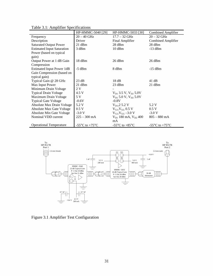
31
Table 3.1: Amplifier Specifications HP-HMMC-5040 [29] HP-HMMC-5033 [30] Combined Amplifier Frequency 20 – 40 GHz 17.7 – 32 GHz 20 – 32 GHz Description Driver Final Amplifier Combined Amplifier Saturated Output Power 21 dBm 28 dBm 28 dBm Estimated Input Saturation Power (based on typical gain)
3 dBm 10 dBm -13 dBm
Output Power at 1 dB Gain Compression
18 dBm 26 dBm 26 dBm
Estimated Input Power 1dB Gain Compression (based on typical gain)
-5 dBm 8 dBm -15 dBm
Typical Gain @ 28 GHz 23 dB 18 dB 41 dB Max Input Power 21 dBm 23 dBm 21 dBm Minimum Drain Voltage 2 V - Typical Drain Voltage 4.5 V VD1 3.5 V, VD2 5.0V Maximum Drain Voltage 5 V VD1 5.0 V, VD2 5.0V Typical Gate Voltage -0.6V -0.8V Absolute Max Drain Voltage 5.2 V VD1,2 5.2 V 5.2 V Absolute Max Gate Voltage 0.5 V VG1,VGG 0.5 V 0.5 V Absolute Min Gate Voltage -3.0 V VG1,VGG –3.0 V -3.0 V Nominal VDD current 225 – 300 mA VD1 180 mA, VD2 400
mA 805 – 880 mA
Operational Temperature -55°C to +75°C -55°C to +85°C -55°C to +75°C
Attenuator30 dB
HMMC−5033
P−1 Out 26 dBmSat Out 28 dBm
18 dB Typical Gain
D1
G1
D2
GG
HMMC−5040
P−1 Out 18 dBm23 dB Typical Gain
Sat Out 21 dBm
GD
2.4 mm female
Port 1HP 8517B
To
Port 2HP 8517B
2.4 mm male
To
3.5 V240 mA
5.0 V460 mA
4.5 V300 mA
1 uF1 uF
−0.8 V
4.7 uF 4.7 uF
−0.6 V
Figure 3.1 Amplifier Test Configuration
32
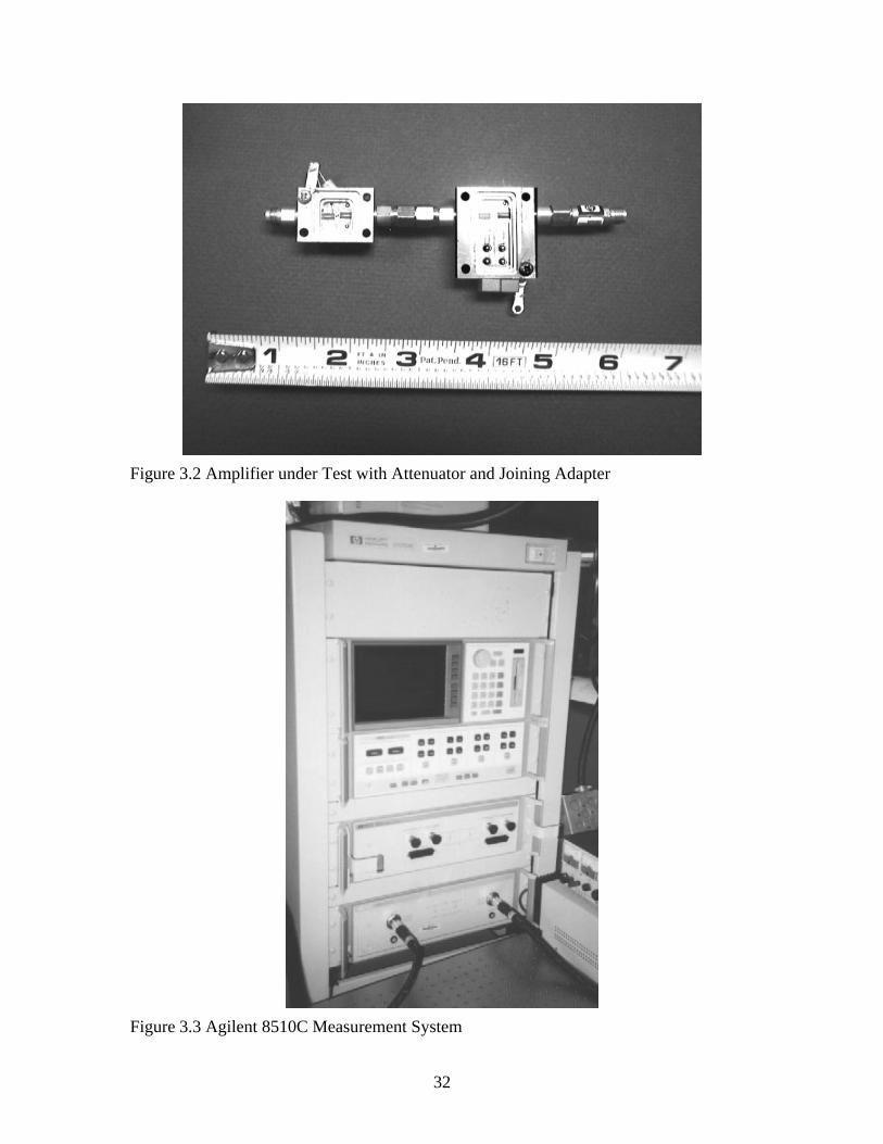
Figure 3.2 Amplifier under Test with Attenuator and Joining Adapter
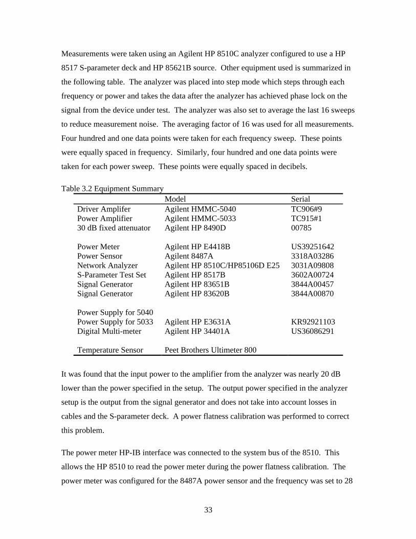
Figure 3.3 Agilent 8510C Measurement System
33
Measurements were taken using an Agilent HP 8510C analyzer configured to use a HP
8517 S-parameter deck and HP 85621B source. Other equipment used is summarized in
the following table. The analyzer was placed into step mode which steps through each
frequency or power and takes the data after the analyzer has achieved phase lock on the
signal from the device under test. The analyzer was also set to average the last 16 sweeps
to reduce measurement noise. The averaging factor of 16 was used for all measurements.
Four hundred and one data points were taken for each frequency sweep. These points
were equally spaced in frequency. Similarly, four hundred and one data points were
taken for each power sweep. These points were equally spaced in decibels.
Table 3.2 Equipment Summary Model Serial Driver Amplifer Agilent HMMC-5040 TC906#9 Power Amplifier Agilent HMMC-5033 TC915#1 30 dB fixed attenuator Agilent HP 8490D 00785 Power Meter Agilent HP E4418B US39251642 Power Sensor Agilent 8487A 3318A03286 Network Analyzer Agilent HP 8510C/HP85106D E25 3031A09808 S-Parameter Test Set Agilent HP 8517B 3602A00724 Signal Generator Agilent HP 83651B 3844A00457 Signal Generator Agilent HP 83620B 3844A00870 Power Supply for 5040 Power Supply for 5033 Agilent HP E3631A KR92921103 Digital Multi-meter Agilent HP 34401A US36086291 Temperature Sensor Peet Brothers Ultimeter 800
It was found that the input power to the amplifier from the analyzer was nearly 20 dB
lower than the power specified in the setup. The output power specified in the analyzer
setup is the output from the signal generator and does not take into account losses in
cables and the S-parameter deck. A power flatness calibration was performed to correct
this problem.
The power meter HP-IB interface was connected to the system bus of the 8510. This
allows the HP 8510 to read the power meter during the power flatness calibration. The
power meter was configured for the 8487A power sensor and the frequency was set to 28

34
GHz. The power meter was then zeroed and then calibrated to the RF source on the front
panel of the power meter. The power of the Port 1 source was set to 10 dBm. Port 1 of
the HP 8517 was connected to the HP 8487A power sensor and a power flatness
calibration was performed. More information on the procedure can be found in Agilent
product note 8510-16 entitled “Controlling Test Port Output Power Flatness” [31].
The output power was confirmed after power calibration for several output powers at
28.0 GHz. The results are shown in the table below.
Table 3.3 Recorded Output Power after Flatness Correction Set Power Measured Power -12 dBm -12.01 dBm -20 dBm -20.05 dBm -25 dBm -25.16 dBm -30 dBm -30.65 dBm
A full 2-port calibration procedure was attempted with the 30 dB fixed attenuator
considered as part of the test set-up. The resulting measurements contained increased
noise because of the noise captured during the calibration with the 30 dB fixed attenuator.
It was decided to remove the 30 dB fixed attenuator from the measurement setup during
calibration. The 30 dB fixed attenuator was then characterized so its effect could be
removed from the measurements later.
A full 2-port calibration without the attenuator was made after the power was leveled.
The male-to-female adapter from the 2.4 mm calibration kit was placed on the Port 1
cable during calibration. Although not required to complete the calibration, the insertion
of this connector during calibration compensates for the insertion of the male-to-male
adapter required at the input of the HMMC-5040 driver amplifier during measurements.
The HMMC-5033 can be biased in one of two ways. The power connections for the
device consist of two drain (VD1, VD2) and two gate connections (VG1,VGG). The first
method of biasing consists of 3 supply voltages of 3.5 V at VD1, 5 V at VD2, and –0.8 V at
VGG with no connection to VG1. VG1 is biased internally from VGG to give the desired
ratio of current between I D1 and I D2. The second biasing configuration connects the VD1
and VD2 to the same 5.0 V supply and connects VG1 and VGG to the same –0.8 V supply.
35
This configuration provides equal I D1 and I D2. All measurements were performed with
the first bias configuration.
Four measurements were taken for each variation when applicable. Frequency sweeps
were performed between 27.5 GHz and 28.5 GHz for powers of –12 dBm and –20 dBm.
This was performed to see the variations in the saturation power with frequency. The
maximum calibrated 28 GHz output power of the analyzer at the input of the amplifier
was found to be -12 dBm. The lowest power possible in a single sweep was -30 dBm.
For power sweeps, the S21 or forward gain of the amplifier was measured with varying
input powers from -30 dBm to -12 dBm or just where the final amplifier HMMC-5033
began to approach saturation. An additional sweep not presented here was made from
-40 dBm to -22 dBm to confirm that the amplifier exhibited a linear response at an input
power of -30 dBm.
Table 3.4 Measurement Types Type Sweep Type Range Constant 1 Frequency 27.5 GHz – 28.5 GHz -20 dBm 2 Frequency 27.5 GHz – 28.5 GHz -12 dBm 4 Power -30 dBm to -12 dBm 28 GHz 5 Power -40 dBm to -22 dBm 28 GHz
Measurements were taken on both HP-HMMC-5040 alone and the combined amplifier
made from the HP-HMMC-5040 and HP-HMMC-5033. The combined amplifier was
tested with several different variations in frequency, drain current, drain voltage, and
device temperature. The bias conditions for each measurement variation are summarized.
An ‘X’ denotes bias conditions such as the gate current that are not important or not
applicable. The following table summarizes the variations.
36
Table 3.5 Measurement Variation Summary Variation Conditions 12 Ideal bias, No cooling 13 Ideal bias, No cooling, Power sweeps at 27.5 GHz and 27.6 GHz 14 VD1 and VD2 on 5033 lowered 10% on 5033, No cooling 15 VG2 on 5033 changed to drop ID by 10%, No cooling 17 VG2 on 5033 changed to drop ID by 10%, Cooled to 51° F
The ideal bias and no cooling measurement is used as a reference for comparison with the
other variation in amplifier conditions. Power sweeps were made at different frequencies
to determine the effect of changing of frequency on the AM-AM and AM-PM
characteristics of the amplifier. Variations 14 and 15 were performed to determine the
effects of non-ideal biasing on the AM-AM and AM-PM characteristics of the amplifier.
The temperature of the amplifier was cooled using a Peltier effect device. The case
temperature of the HMMC-5040 amplifier was measured using the Peet Brothers
Ultimeter 800 temperature sensor.
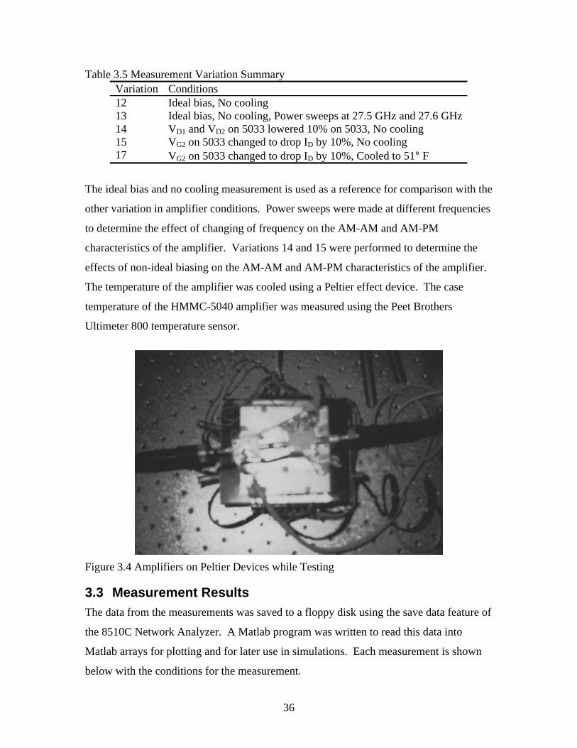
Figure 3.4 Amplifiers on Peltier Devices while Testing
3.3 Measurement Results The data from the measurements was saved to a floppy disk using the save data feature of
the 8510C Network Analyzer. A Matlab program was written to read this data into
Matlab arrays for plotting and for later use in simulations. Each measurement is shown
below with the conditions for the measurement.
37
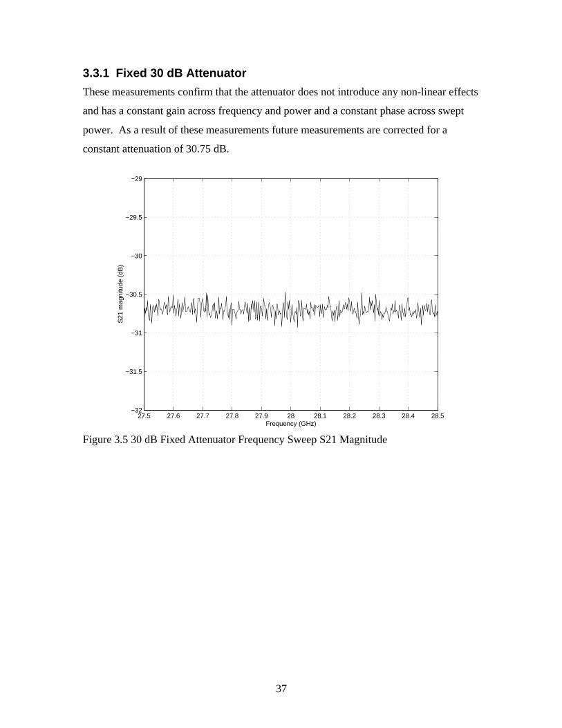
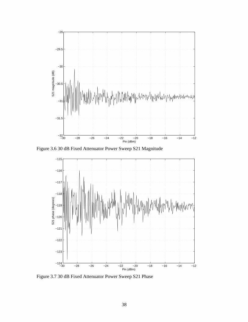
3.3.1 Fixed 30 dB Attenuator
These measurements confirm that the attenuator does not introduce any non-linear effects
and has a constant gain across frequency and power and a constant phase across swept
power. As a result of these measurements future measurements are corrected for a
constant attenuation of 30.75 dB.
27.5 27.6 27.7 27.8 27.9 28 28.1 28.2 28.3 28.4 28.5−32
−31.5
−31
−30.5
−30
−29.5
−29
Frequency (GHz)
S21
mag
nitu
de (
dB)
Figure 3.5 30 dB Fixed Attenuator Frequency Sweep S21 Magnitude
38
−30 −28 −26 −24 −22 −20 −18 −16 −14 −12−32
−31.5
−31
−30.5
−30
−29.5
−29
Pin (dBm)
S21
mag
nitu
de (
dB)
Figure 3.6 30 dB Fixed Attenuator Power Sweep S21 Magnitude
−30 −28 −26 −24 −22 −20 −18 −16 −14 −12−124
−123
−122
−121
−120
−119
−118
−117
−116
−115
Pin (dBm)
S21
pha
se (
degr
ees)
Figure 3.7 30 dB Fixed Attenuator Power Sweep S21 Phase
39
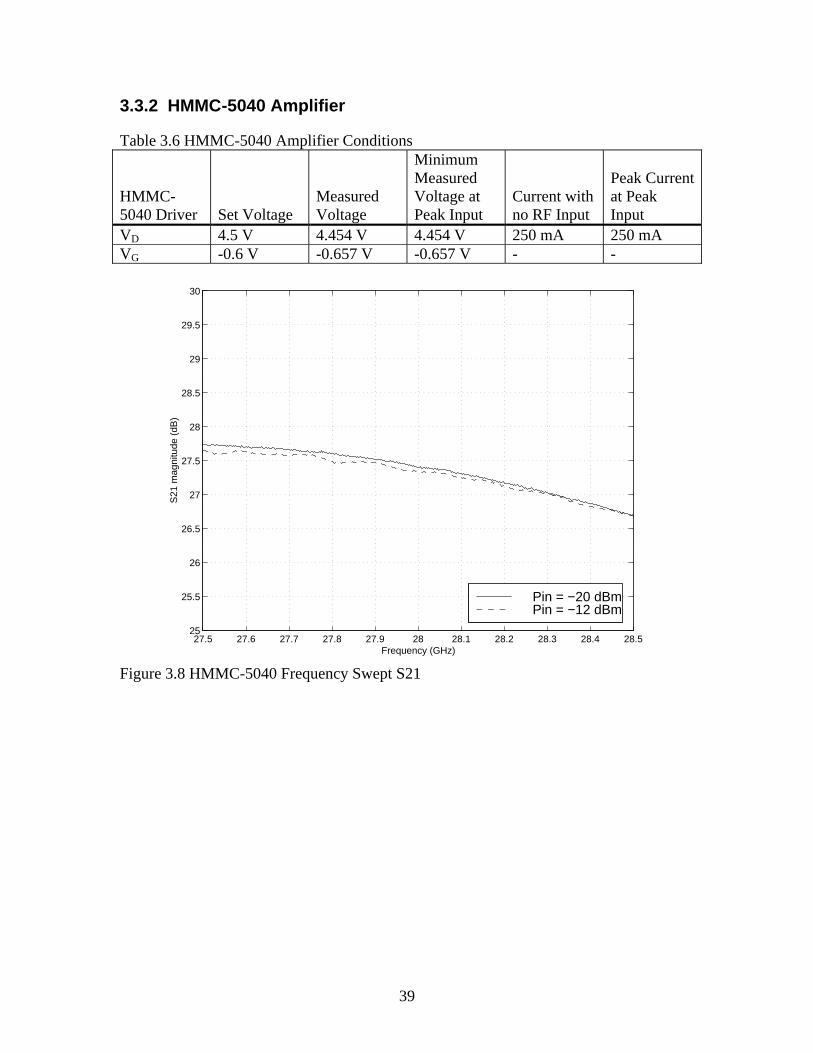
3.3.2 HMMC-5040 Amplifier
Table 3.6 HMMC-5040 Amplifier Conditions
HMMC-5040 Driver Set Voltage
Measured Voltage
Minimum Measured Voltage at Peak Input
Current with no RF Input
Peak Current at Peak Input
VD 4.5 V 4.454 V 4.454 V 250 mA 250 mA VG -0.6 V -0.657 V -0.657 V - -
27.5 27.6 27.7 27.8 27.9 28 28.1 28.2 28.3 28.4 28.525
25.5
26
26.5
27
27.5
28
28.5
29
29.5
30
Frequency (GHz)
S21
mag
nitu
de (
dB)
Pin = −20 dBmPin = −12 dBm
Figure 3.8 HMMC-5040 Frequency Swept S21
40
−30 −28 −26 −24 −22 −20 −18 −16 −14 −1225
25.5
26
26.5
27
27.5
28
28.5
29
29.5
30
Pin (dBm)
S21
mag
nitu
de (
dB)
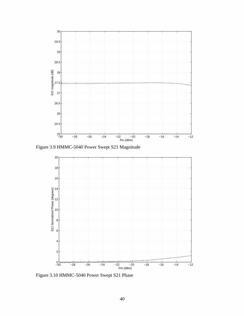
Figure 3.9 HMMC-5040 Power Swept S21 Magnitude
−30 −28 −26 −24 −22 −20 −18 −16 −14 −120
2
4
6
8
10
12
14
16
18
20
Pin (dBm)
S21
Nor
mal
ized
Pha
se (
degr
ees)
Figure 3.10 HMMC-5040 Power Swept S21 Phase
41
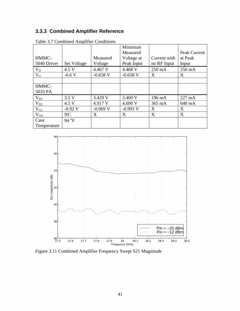
3.3.3 Combined Amplifier Reference
Table 3.7 Combined Amplifier Conditions
HMMC-5040 Driver Set Voltage
Measured Voltage
Minimum Measured Voltage at Peak Input
Current with no RF Input
Peak Current at Peak Input
VD 4.5 V 4.467 V 4.468 V 250 mA 250 mA VG -0.6 V -0.658 V -0.658 V X X HMMC-5033 PA
VD1 3.5 V 3.429 V 3.400 V 196 mA 227 mA VD2 4.5 V 4.917 V 4.600 V 365 mA 640 mA VG1 -0.92 V -0.969 V -0.993 V X X VGG NC X X X X Case Temperature
94 °F
27.5 27.6 27.7 27.8 27.9 28 28.1 28.2 28.3 28.4 28.536
38
40
42
44
46
48
Frequency (GHz)
S21
mag
nitu
de (
dB)
Pin = −20 dBmPin = −12 dBm
Figure 3.11 Combined Amplifier Frequency Swept S21 Magnitude
42
−30 −28 −26 −24 −22 −20 −18 −16 −14 −1236
38
40
42
44
46
48
Pin (dBm)
S21
mag
nitu
de (
dB)
Figure 3.12 Combined Amplifier Power Swept S21 Magnitude
−30 −28 −26 −24 −22 −20 −18 −16 −14 −120
2
4
6
8
10
12
14
16
18
20
Pin (dBm)
S21
Nor
mal
ized
Pha
se (
degr
ees)
Figure 3.13 Combined Amplifer Power Swept S21 Phase
43
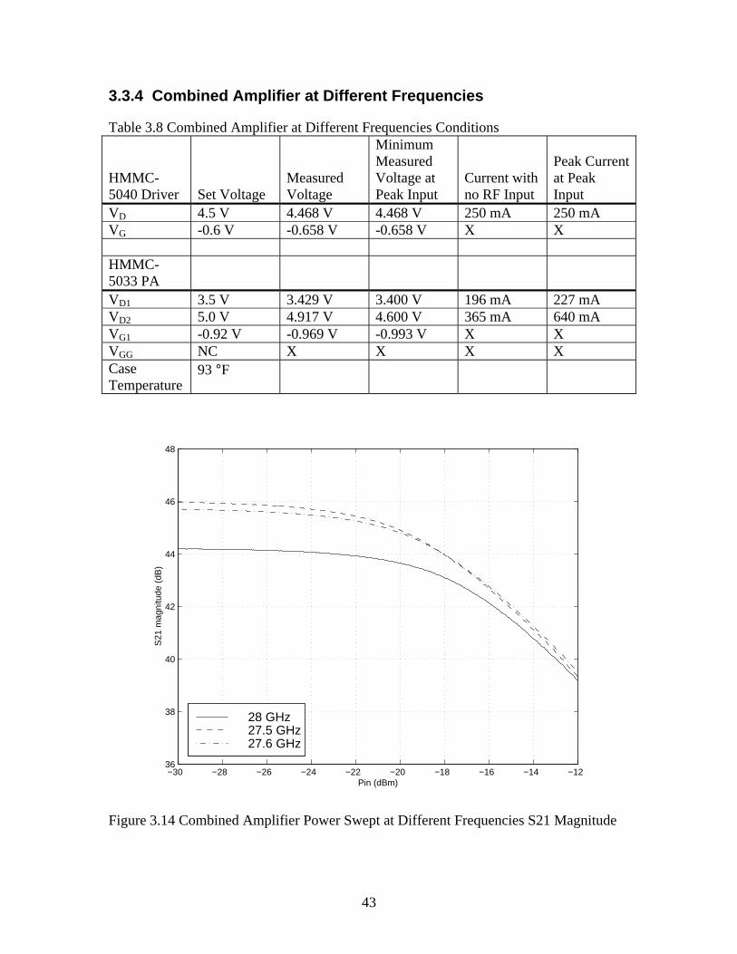
3.3.4 Combined Amplifier at Different Frequencies
Table 3.8 Combined Amplifier at Different Frequencies Conditions
HMMC-5040 Driver Set Voltage
Measured Voltage
Minimum Measured Voltage at Peak Input
Current with no RF Input
Peak Current at Peak Input
VD 4.5 V 4.468 V 4.468 V 250 mA 250 mA VG -0.6 V -0.658 V -0.658 V X X HMMC-5033 PA
VD1 3.5 V 3.429 V 3.400 V 196 mA 227 mA VD2 5.0 V 4.917 V 4.600 V 365 mA 640 mA VG1 -0.92 V -0.969 V -0.993 V X X VGG NC X X X X Case Temperature
93 °F
−30 −28 −26 −24 −22 −20 −18 −16 −14 −1236
38
40
42
44
46
48
Pin (dBm)
S21
mag
nitu
de (
dB)
28 GHz27.5 GHz27.6 GHz
Figure 3.14 Combined Amplifier Power Swept at Different Frequencies S21 Magnitude
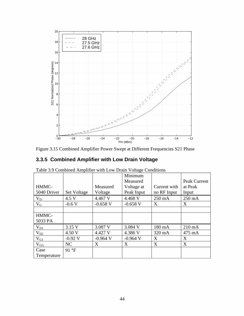
44
−30 −28 −26 −24 −22 −20 −18 −16 −14 −120
2
4
6
8
10
12
14
16
18
20
Pin (dBm)
S21
Nor
mal
ized
Pha
se (
degr
ees)
28 GHz27.5 GHz27.6 GHz
Figure 3.15 Combined Amplifier Power Swept at Different Frequencies S21 Phase
3.3.5 Combined Amplifier with Low Drain Voltage
Table 3.9 Combined Amplifier with Low Drain Voltage Conditions
HMMC-5040 Driver Set Voltage
Measured Voltage
Minimum Measured Voltage at Peak Input
Current with no RF Input
Peak Current at Peak Input
VD 4.5 V 4.467 V 4.468 V 250 mA 250 mA VG -0.6 V -0.658 V -0.658 V X X HMMC-5033 PA
VD1 3.15 V 3.087 V 3.084 V 180 mA 210 mA VD2 4.50 V 4.427 V 4.386 V 320 mA 475 mA VG1 -0.92 V -0.964 V -0.964 V X X VGG NC X X X X Case Temperature
91 °F
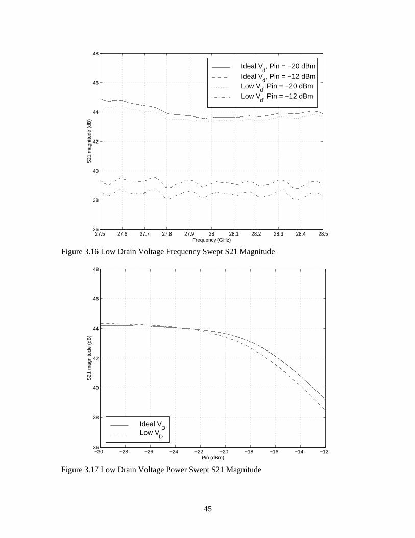
45
27.5 27.6 27.7 27.8 27.9 28 28.1 28.2 28.3 28.4 28.536
38
40
42
44
46
48
Frequency (GHz)
S21
mag
nitu
de (
dB)
Ideal Vd, Pin = −20 dBm
Ideal Vd, Pin = −12 dBm
Low Vd, Pin = −20 dBm
Low Vd, Pin = −12 dBm
Figure 3.16 Low Drain Voltage Frequency Swept S21 Magnitude
−30 −28 −26 −24 −22 −20 −18 −16 −14 −1236
38
40
42
44
46
48
Pin (dBm)
S21
mag
nitu
de (
dB)
Ideal VD
Low VD
Figure 3.17 Low Drain Voltage Power Swept S21 Magnitude
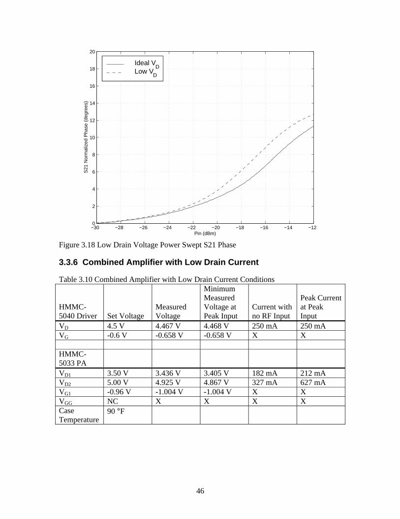
46
−30 −28 −26 −24 −22 −20 −18 −16 −14 −120
2
4
6
8
10
12
14
16
18
20
Pin (dBm)
S21
Nor
mal
ized
Pha
se (
degr
ees)
Ideal VD
Low VD
Figure 3.18 Low Drain Voltage Power Swept S21 Phase
3.3.6 Combined Amplifier with Low Drain Current
Table 3.10 Combined Amplifier with Low Drain Current Conditions
HMMC-5040 Driver Set Voltage
Measured Voltage
Minimum Measured Voltage at Peak Input
Current with no RF Input
Peak Current at Peak Input
VD 4.5 V 4.467 V 4.468 V 250 mA 250 mA VG -0.6 V -0.658 V -0.658 V X X HMMC-5033 PA
VD1 3.50 V 3.436 V 3.405 V 182 mA 212 mA VD2 5.00 V 4.925 V 4.867 V 327 mA 627 mA VG1 -0.96 V -1.004 V -1.004 V X X VGG NC X X X X Case Temperature
90 °F
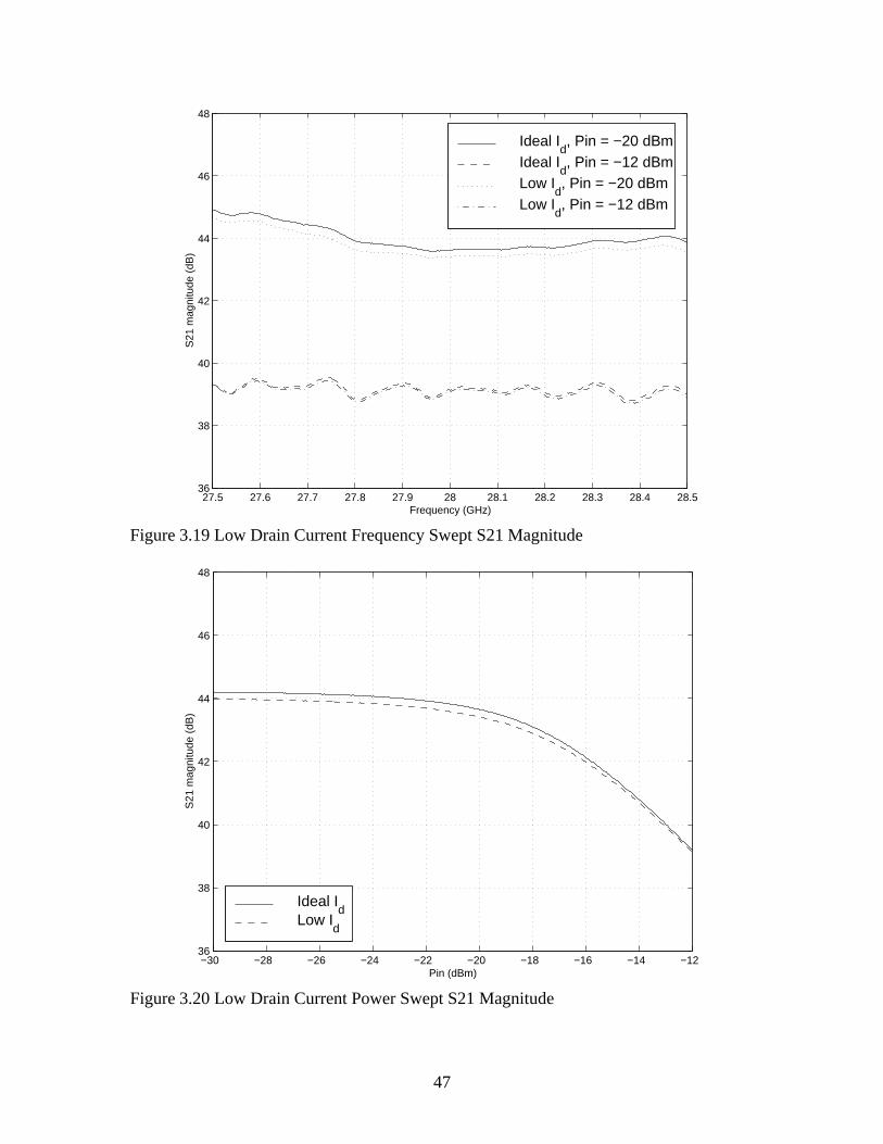
47
27.5 27.6 27.7 27.8 27.9 28 28.1 28.2 28.3 28.4 28.536
38
40
42
44
46
48
Frequency (GHz)
S21
mag
nitu
de (
dB)
Ideal Id, Pin = −20 dBm
Ideal Id, Pin = −12 dBm
Low Id, Pin = −20 dBm
Low Id, Pin = −12 dBm
Figure 3.19 Low Drain Current Frequency Swept S21 Magnitude
−30 −28 −26 −24 −22 −20 −18 −16 −14 −1236
38
40
42
44
46
48
Pin (dBm)
S21
mag
nitu
de (
dB)
Ideal Id
Low Id
Figure 3.20 Low Drain Current Power Swept S21 Magnitude
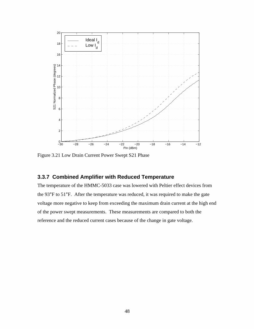
48
−30 −28 −26 −24 −22 −20 −18 −16 −14 −120
2
4
6
8
10
12
14
16
18
20
Pin (dBm)
S21
Nor
mal
ized
Pha
se (
degr
ees)
Ideal Id
Low Id
Figure 3.21 Low Drain Current Power Swept S21 Phase
3.3.7 Combined Amplifier with Reduced Temperature
The temperature of the HMMC-5033 case was lowered with Peltier effect devices from
the 93°F to 51°F. After the temperature was reduced, it was required to make the gate
voltage more negative to keep from exceeding the maximum drain current at the high end
of the power swept measurements. These measurements are compared to both the
reference and the reduced current cases because of the change in gate voltage.
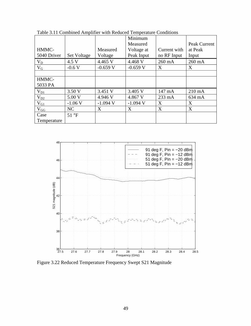
49
Table 3.11 Combined Amplifier with Reduced Temperature Conditions
HMMC-5040 Driver Set Voltage
Measured Voltage
Minimum Measured Voltage at Peak Input
Current with no RF Input
Peak Current at Peak Input
VD 4.5 V 4.465 V 4.468 V 260 mA 260 mA VG -0.6 V -0.659 V -0.659 V X X HMMC-5033 PA
VD1 3.50 V 3.451 V 3.405 V 147 mA 210 mA VD2 5.00 V 4.946 V 4.867 V 233 mA 634 mA VG1 -1.06 V -1.094 V -1.094 V X X VGG NC X X X X Case Temperature
51 °F
27.5 27.6 27.7 27.8 27.9 28 28.1 28.2 28.3 28.4 28.536
38
40
42
44
46
48
Frequency (GHz)
S21
mag
nitu
de (
dB)
91 deg F, Pin = −20 dBm91 deg F, Pin = −12 dBm51 deg F, Pin = −20 dBm51 deg F, Pin = −12 dBm
Figure 3.22 Reduced Temperature Frequency Swept S21 Magnitude
50
−30 −28 −26 −24 −22 −20 −18 −16 −14 −1236
38
40
42
44
46
48
Pin (dBm)
S21
mag
nitu
de (
dB)
91 deg F Reference51 deg F91 deg F Low I
D
Figure 3.23 Reduced Temperature Power Swept S21 Magnitude
−30 −28 −26 −24 −22 −20 −18 −16 −14 −120
2
4
6
8
10
12
14
16
18
20
Pin (dBm)
S21
Nor
mal
ized
Pha
se (
degr
ees)
91 deg F Reference51 deg F91 deg F Low I
D
Figure 3.24 Reduced Temperature Power Swept S21 Phase
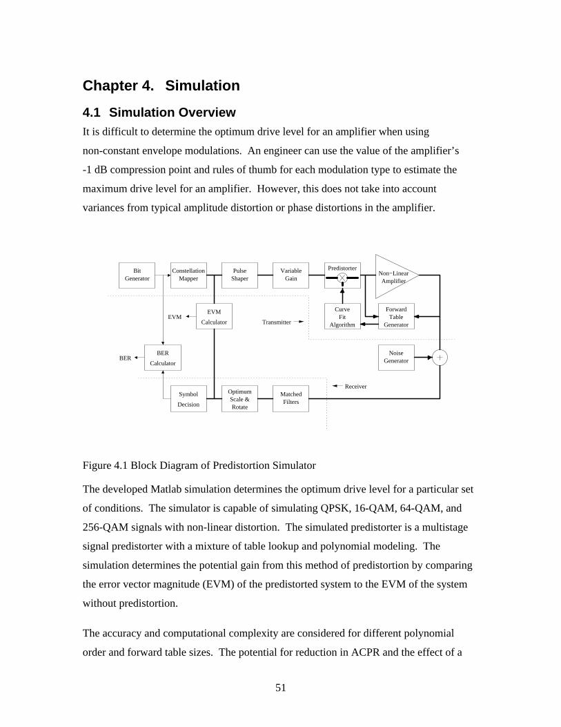
51
Chapter 4. Simulation
4.1 Simulation Overview It is difficult to determine the optimum drive level for an amplifier when using
non-constant envelope modulations. An engineer can use the value of the amplifier’s
-1 dB compression point and rules of thumb for each modulation type to estimate the
maximum drive level for an amplifier. However, this does not take into account
variances from typical amplitude distortion or phase distortions in the amplifier.
MapperConstellation Pulse
Shaper
Calculator
EVM
Calculator
BER
Decision
SymbolScale &Rotate
Optimum MatchedFilters
BitGenerator
VariableGain
Non−LinearAmplifier
TableGenerator
Forward
Predistorter
GeneratorNoise
CurveFit
Algorithm
BER
EVMTransmitter
Receiver
Figure 4.1 Block Diagram of Predistortion Simulator
The developed Matlab simulation determines the optimum drive level for a particular set
of conditions. The simulator is capable of simulating QPSK, 16-QAM, 64-QAM, and
256-QAM signals with non-linear distortion. The simulated predistorter is a multistage
signal predistorter with a mixture of table lookup and polynomial modeling. The
simulation determines the potential gain from this method of predistortion by comparing
the error vector magnitude (EVM) of the predistorted system to the EVM of the system
without predistortion.
The accuracy and computational complexity are considered for different polynomial
order and forward table sizes. The potential for reduction in ACPR and the effect of a

52
maladjusted predistorter are also considered. The next chapter uses the insight on design
decisions gained from these simulations to evaluate the feasibility of a proposed
predistorter for a LMDS system.
4.2 Simulation Design
4.2.1 Transmitter
4.2.1.1 Random Sequence Generator The random sequence generator generates a bit sequence of either one or zero with equal
probability. The sequence length is specified when the sequence is generated.
4.2.1.2 Constellation Generator The constellation generator converts the bit sequence from zeros and ones to a complex
valued constellation point. The generator is capable of generating QPSK, 16-QAM,
64-QAM, and 256-QAM signals. Grey coding was used in assigning binary values to
each point so errors with adjacent symbols would cause a single bit error. The
constellations and decimal values assigned to each symbol are shown in the following
figures. The peak power of each constellation is 1W with corresponding peak I and Q
voltages of 21 volt.
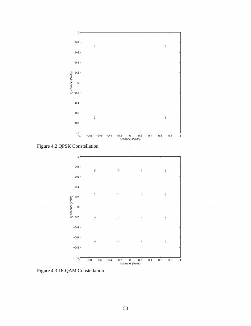
53
−1 −0.8 −0.6 −0.4 −0.2 0 0.2 0.4 0.6 0.8 1−1
−0.8
−0.6
−0.4
−0.2
0
0.2
0.4
0.6
0.8
1
I channel (Volts)
Q c
hann
el (
Vol
ts)
0 1
2 3
Figure 4.2 QPSK Constellation
−1 −0.8 −0.6 −0.4 −0.2 0 0.2 0.4 0.6 0.8 1−1
−0.8
−0.6
−0.4
−0.2
0
0.2
0.4
0.6
0.8
1
I channel (Volts)
Q c
hann
el (
Vol
ts)
0 1
2 3
4 5
6 7
89
1011
1213
1415
Figure 4.3 16-QAM Constellation
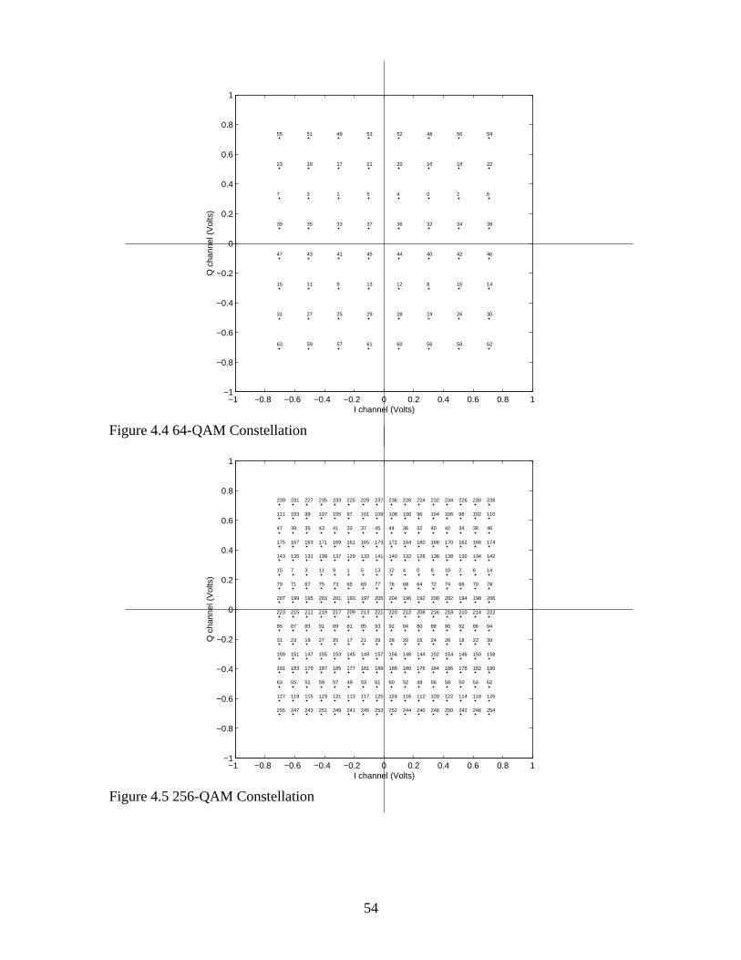
54
−1 −0.8 −0.6 −0.4 −0.2 0 0.2 0.4 0.6 0.8 1−1
−0.8
−0.6
−0.4
−0.2
0
0.2
0.4
0.6
0.8
1
I channel (Volts)
Q c
hann
el (
Vol
ts)
01 23 45 67
89 1011 1213 1415
1617 1819 2021 2223
2425 2627 2829 3031
3233 3435 3637 3839
4041 4243 4445 4647
4849 5051 5253 5455
5657 5859 6061 6263
Figure 4.4 64-QAM Constellation
−1 −0.8 −0.6 −0.4 −0.2 0 0.2 0.4 0.6 0.8 1−1
−0.8
−0.6
−0.4
−0.2
0
0.2
0.4
0.6
0.8
1
I channel (Volts)
Q c
hann
el (
Vol
ts)
01 23 45 67 89 1011 1213 1415
1617 1819 2021 2223 2425 2627 2829 3031
3233 3435 3637 3839 4041 4243 4445 4647
4849 5051 5253 5455 5657 5859 6061 6263
6465 6667 6869 7071 7273 7475 7677 7879
8081 8283 8485 8687 8889 9091 9293 9495
9697 9899 100101 102103 104105 106107 108109 110111
112113 114115 116117 118119 120121 122123 124125 126127
128129 130131 132133 134135 136137 138139 140141 142143
144145 146147 148149 150151 152153 154155 156157 158159
160161 162163 164165 166167 168169 170171 172173 174175
176177 178179 180181 182183 184185 186187 188189 190191
192193 194195 196197 198199 200201 202203 204205 206207
208209 210211 212213 214215 216217 218219 220221 222223
224225 226227 228229 230231 232233 234235 236237 238239
240241 242243 244245 246247 248249 250251 252253 254255
Figure 4.5 256-QAM Constellation

55
4.2.1.3 Root Raised Cosine Pulse Shaping The ideal root raised cosine filter has an infinite length and must be truncated when
implemented. The delay of 6 symbols was found experimentally by increasing the delay
until the error due to the truncated filter was small compared to other errors. An
oversampling rate of 8 was used for the simulations; therefore each symbol results in 8
samples. The filter is implemented as a FIR filter with (8 x 6 x 2) + 1 = 97 taps. Each
symbol after filtering depends on the values of the six symbols before and the six
symbols after the symbol of interest.
The root raised cosine filter rolloff factor affects the shape of the filter. A filter with a
rolloff factor of 1 has a gradual cutoff while a filter with a rolloff factor of 0 is an ideal
low pass filter. Rolloff factors (r) of 0.15, 0.2, 0.35, and 0.5 are considered in the
simulations. The rolloff factors of 0.2 and 0.35 are specified in the DAVIC standard for
LMDS systems [32].
−6 −4 −2 0 2 4 6−0.1
0
0.1
0.2
0.3
0.4
0.5
0.6
Symbols
Am
plitu
de
Square−root r=0.5Square−root r=0.15
Figure 4.6 Root-Raise Cosine Impulse Response for r=0.5 and r=0.15.

56
−6 −4 −2 0 2 4 6−0.2
0
0.2
0.4
0.6
0.8
1
1.2
Symbols
Am
plitu
de
Square−root r=0.5r=0.5
Figure 4.7 Comparison of Root-Raised Cosine Filter and Raised Cosine Filter
4.2.1.4 Adjustable Gain Block An adjustable gain block is before the predistorter to increase or decrease the input power
to the amplifier. The adjustable gain value is the independent variable of later plots that
show the point of minimum EVM.
The use of an adjustable gain block was favored over setting a power from the simulated
transmitter because differences in the distortion, root-cosine filter parameters, and
modulation type make referencing a mean or peak power difficult. The data in the peak-
to-average section can be used to determine the peak and average input powers to the
amplifier for a specific modulation, rolloff factor, and adjustable gain block setting.
4.2.1.5 Signal Predistorter The implemented predistorter is a polynomial sample gain predistorter. The predistorter
operates on individual samples and multiples the complex result of the predistortion
function by the input samples.
The predistortion function can be represented in a polar or rectangular form. The
rectangular representation for the function was chosen since the samples are already
rectuangular and will most likely be rectangular in an implementation. The rectangular
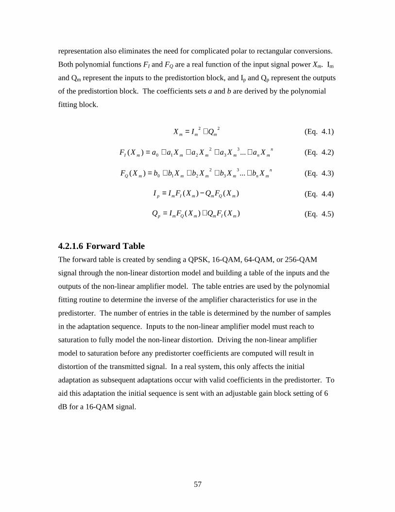
57
representation also eliminates the need for complicated polar to rectangular conversions.
Both polynomial functions FI and FQ are a real function of the input signal power Xm. Im
and Qm represent the inputs to the predistortion block, and Ip and Qp represent the outputs
of the predistortion block. The coefficients sets a and b are derived by the polynomial
fitting block.
22mmm QIX += (Eq. 4.1)
nmnmmmmI XaXaXaXaaXF ++++= ...)( 3
32
210 (Eq. 4.2)
nmnmmmmQ XbXbXbXbbXF ++++= ...)( 3
32
210 (Eq. 4.3)
)()( mQmmImp XFQXFII −= (Eq. 4.4)
)()( mImmQmp XFQXFIQ += (Eq. 4.5)
4.2.1.6 Forward Table The forward table is created by sending a QPSK, 16-QAM, 64-QAM, or 256-QAM
signal through the non-linear distortion model and building a table of the inputs and the
outputs of the non-linear amplifier model. The table entries are used by the polynomial
fitting routine to determine the inverse of the amplifier characteristics for use in the
predistorter. The number of entries in the table is determined by the number of samples
in the adaptation sequence. Inputs to the non-linear amplifier model must reach to
saturation to fully model the non-linear distortion. Driving the non-linear amplifier
model to saturation before any predistorter coefficients are computed will result in
distortion of the transmitted signal. In a real system, this only affects the initial
adaptation as subsequent adaptations occur with valid coefficients in the predistorter. To
aid this adaptation the initial sequence is sent with an adjustable gain block setting of 6
dB for a 16-QAM signal.
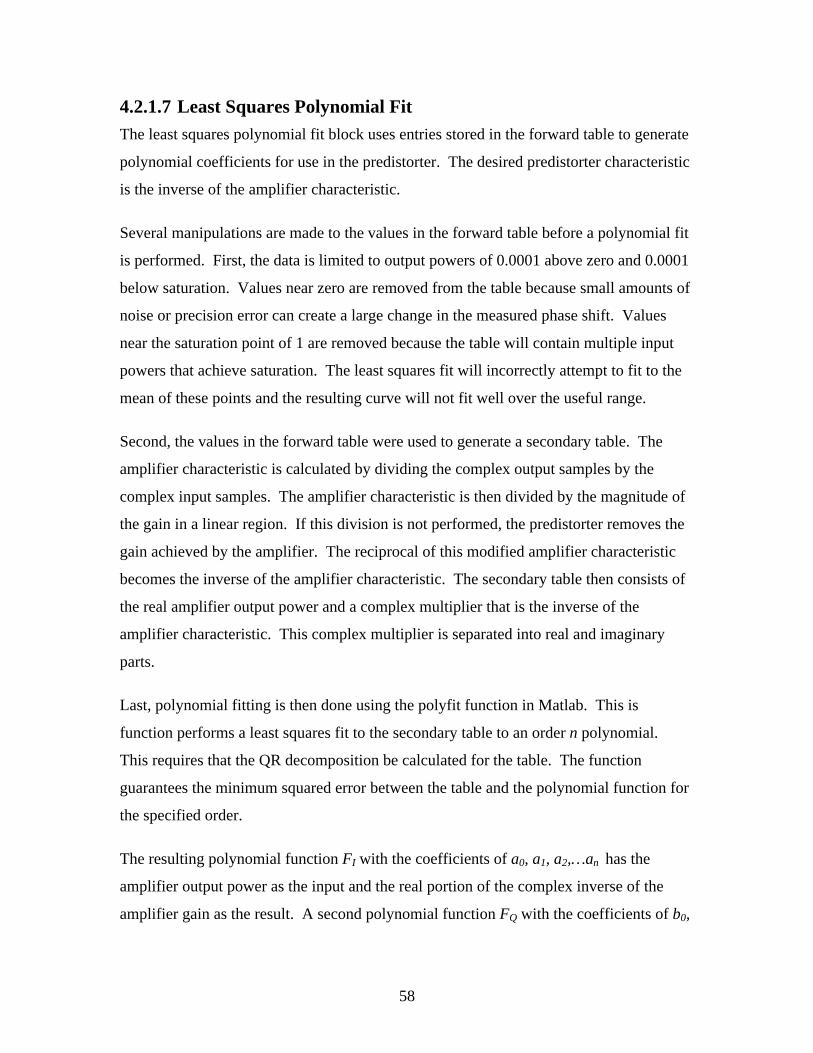
58
4.2.1.7 Least Squares Polynomial Fit The least squares polynomial fit block uses entries stored in the forward table to generate
polynomial coefficients for use in the predistorter. The desired predistorter characteristic
is the inverse of the amplifier characteristic.
Several manipulations are made to the values in the forward table before a polynomial fit
is performed. First, the data is limited to output powers of 0.0001 above zero and 0.0001
below saturation. Values near zero are removed from the table because small amounts of
noise or precision error can create a large change in the measured phase shift. Values
near the saturation point of 1 are removed because the table will contain multiple input
powers that achieve saturation. The least squares fit will incorrectly attempt to fit to the
mean of these points and the resulting curve will not fit well over the useful range.
Second, the values in the forward table were used to generate a secondary table. The
amplifier characteristic is calculated by dividing the complex output samples by the
complex input samples. The amplifier characteristic is then divided by the magnitude of
the gain in a linear region. If this division is not performed, the predistorter removes the
gain achieved by the amplifier. The reciprocal of this modified amplifier characteristic
becomes the inverse of the amplifier characteristic. The secondary table then consists of
the real amplifier output power and a complex multiplier that is the inverse of the
amplifier characteristic. This complex multiplier is separated into real and imaginary
parts.
Last, polynomial fitting is then done using the polyfit function in Matlab. This is
function performs a least squares fit to the secondary table to an order n polynomial.
This requires that the QR decomposition be calculated for the table. The function
guarantees the minimum squared error between the table and the polynomial function for
the specified order.
The resulting polynomial function FI with the coefficients of a0, a1, a2,…an has the
amplifier output power as the input and the real portion of the complex inverse of the
amplifier gain as the result. A second polynomial function FQ with the coefficients of b0,

59
b1, b2,…bn also has the amplifier output power as the input and the imaginary part of the
complex inverse of the amplifier gain as the result.
4.2.1.8 Non-Linear Distortion The non-linear distortion is based upon the AM-AM and AM-PM distortion
characteristics of the measured Agilent HMMC-5040 and HMMC-5033 combined
amplifier. The simulation reads the characteristics from a data file saved by an HP
network analyzer.
The gain of the measured amplifier was scaled so that 1 was the maximum output power
and the amplifier presented unity gain while operating in the linear region. Several
special cases were required to extend the model if the input was outside of the measured
amplifier characteristics or was not an exact measured value.
If the input to the non-linear block is within the range of measured values then cubic
interpolation is used to determine the output magnitude and phase distortion. The
resulting response passes through every measured point and an interpolation is made if
the input is between two measured points. This is in contrast to the polynomial fit used in
the predistorter, which computes a ‘best fit’ for all data points and does not necessarily
pass through the fitted points. The accuracy of cubic interpolation outside the measured
points was found to be poor so, further cases were needed.
If the input to the non-linear distortion block is below the measured values, then the gain
of the amplifier is linear with a gain equal to the gain at the lowest measured power.
Scaling makes this gain unity for the reference amplifier. The phase shift is held equal to
the phase shift at the lowest measured power. This is valid if the stored measurements
extend into the linear region of the amplifier.
The output of the non-linear distortion is limited to the highest measured output power if
the input to the non-linear model is above the highest measured value. The phase
distortion is continued with a linear slope that is determined by the point at the highest
power and 5% below the highest power. This is valid if the stored measurements extend
into the saturation region of the amplifier.

60
4.2.2 Receiver
4.2.2.1 Noise Generator The noise generator adds additive white Gaussian noise to the signal before it is received.
In a real system, the signal at this point would be a real bandpass signal. Since the
simulated signal is baseband, independent noise with half the power of the desired
bandpass noise power is added to both the I and Q channels. The bandpass noise power
when expressed in decibels is relative to the peak constellation power of 1 W.
4.2.2.2 Scaling and Rotation This block is analogous to automatic gain control (AGC) and carrier synchronization in a
real receiver. The input amplitude to the receiver varies as the adjustable gain block
changes the input amplitude to the non-linear amplifier. The varying gain in the non-
linear distortion also changes the amplitude at the receiver. The phase distortion in the
non-linear distortion model can offset the phase of the constellation. In a real receiver,
carrier synchronization will correct a constant phase offset of the constellation. Since the
simulation is performed on a baseband signal, carrier synchronization is not needed, but a
correction of a constant phase offset is still required.
To correct these problems, scaling and rotation are applied to the symbols at the output of
the matched filter and before symbol decision. The average I and Q samples for a
particular reference symbol are compared to the ideal values and used to correct each
sample from the matched filter output. The reference symbol for every modulation type
simulated was the upper right corner point. Multiplying the correction factor to the
received symbols rotates and scales the received constellation until the mean of received
symbols that should be interpreted as the chosen reference symbol are the same value as
the transmitted reference signal.
The complex division of the reference ( refref jQI + ) by the mean received signal
( refref ˆˆ QjI + ) for the reference constellation point is used to provide the correction factor.
The correction is then multiplied by all the received samples (QjI ˆˆ + ) to obtain scaled
and rotated received signal.

61
)ˆˆmean()ˆˆ(ˆˆ
refref
refrefscaledscaled
QjI
jQIQjIQjI
+++= ⋅+ (Eq. 4.6)
Because the reference symbol for all modulations considered is the upper right symbol,
non-linear distortions will be the most prominently seen in the constellation points near
the zero power. As the simulated amplifier goes into compression, the inner constellation
points will move toward the outer points. Similarly, the inner points will show the
highest degree of phase distortion.
4.2.2.3 Root Raised Cosine Matched Filters The two root raised cosine matched filters in the receiver are the second half of the
desired raised cosine response. The same length and rolloff factor used in the transmitter
pulse shaper is used here. The I and Q signals are separately filtered. Matrix
multiplication is used compute the filter output at symbol times. This removes the
oversampling and each output then corresponds to a complex mapping of a received
symbol.
4.2.2.4 Symbol Decision The symbol decision routine takes the input I and Q signals and scales the signal so ideal
points are at integer values and then the round function is used to determine the closest
signal point. The I and Q values are then converted to binary and then finally returned to
an array of bits.
4.2.2.5 Error Vector Magnitude The error vector magnitude (EVM) is used as a measure of signal quality. This measure
of performance shows signal degradation before it shows up in bit error measurements.
EVM is used because simulations with a high signal to noise ratio require large
simulation times to acquire statistically significant BER measurements.
The error vector magnitude is calculated by computing the magnitude of the vector
between the received signal ( QjI ˆˆ + ) and the transmitted signal ( jQI + ). The EVM is
defined as the error vector voltage as percentage of the symbol with the highest voltage
[33]. When expressed in decibels it is referenced to the peak power of 1 W.

62
22
22 )ˆ()ˆ(
peakpeak QI
QQIIEVM
+
−+−= (Eq. 4.7)
[33]
If the EVM is shown versus different adjustable gain block levels, the point where EVM
is minimum is the optimum amplifier input level and will result in the best performance
at the receiver.
4.2.2.6 Bit Error Rate The bit error rate is calculated on the stream of bits by the following equation.
bits
errors
N
NBER= (Eq. 4.8)
If no bit errors occur during a sequence, a significantly small bit error of 10-12 is used to
allow plotting on a semi-log graph.
4.3 Simulation Results
4.3.1 Peak-to-Average Ratio
Cavers noticed in [7] that additional backoff was needed for similar performance when
the rolloff factor was decreased to 0.2 but did not present a reason. This happens because
the peak-to-average ratio increases with a reduction in the rolloff factor. This is a result
of increased intersymbol interference (ISI) generated by the root-raised cosine filter. The
peak-to-average ratio also increases when the modulation index is increased due to a
reduction in the mean power.
The mean voltage of the output from the root raised cosine filter was found to vary only
with modulation index. As the rolloff factor was varied from 0.15 to 0.5 the change in
the mean between different rolloffs was found to be less than 0.05 dB and therefore
insignificant. The mean power input to the adjustable gain block can be determined by
the mean powers in the following table. The powers are relative to the peak power output
of 1 from the constellation generator.

63
Table 4.1 Peak-to-Average Ratios for Different Modulations Modulation Mean Power
Relative to Peak Input Power of 1
Mean Power Relative to QPSK
Peak-to-Average Ratio (r = 0.5)
Peak-to-Average Ratio (r = 0.15)
QPSK -9.0330 dB 0 dB 3.3495 dB 6.3187 dB 16-QAM -11.5867 dB -2.5536 dB 5.9032 dB 8.8724 dB 64-QAM -12.7123 dB -3.6793 dB 7.0288 dB 9.9980 dB 256-QAM -13.2643 dB -4.2312 dB 7.5808 dB 10.5500 dB
The peak values were determined by filtering a sequence of symbols with the peak power
in the constellation by the absolute value of the root cosine coefficients. This guaranteed
the contribution from the adjacent points summed and the peak output of this filtering
was considered the peak output voltage. The peak output voltage was found to be
independent of the modulation index and remains almost constant until the rolloff factor
is reduced to below 0.4. The peak output of the filter did not necessarily occur at the
times when a symbol was aligned with the center of the filter. The following graph of the
peak output power from the root-raised cosine filter is relative to the peak input power of
1 and can be used to determine the peak input power to the adjustable gain block.
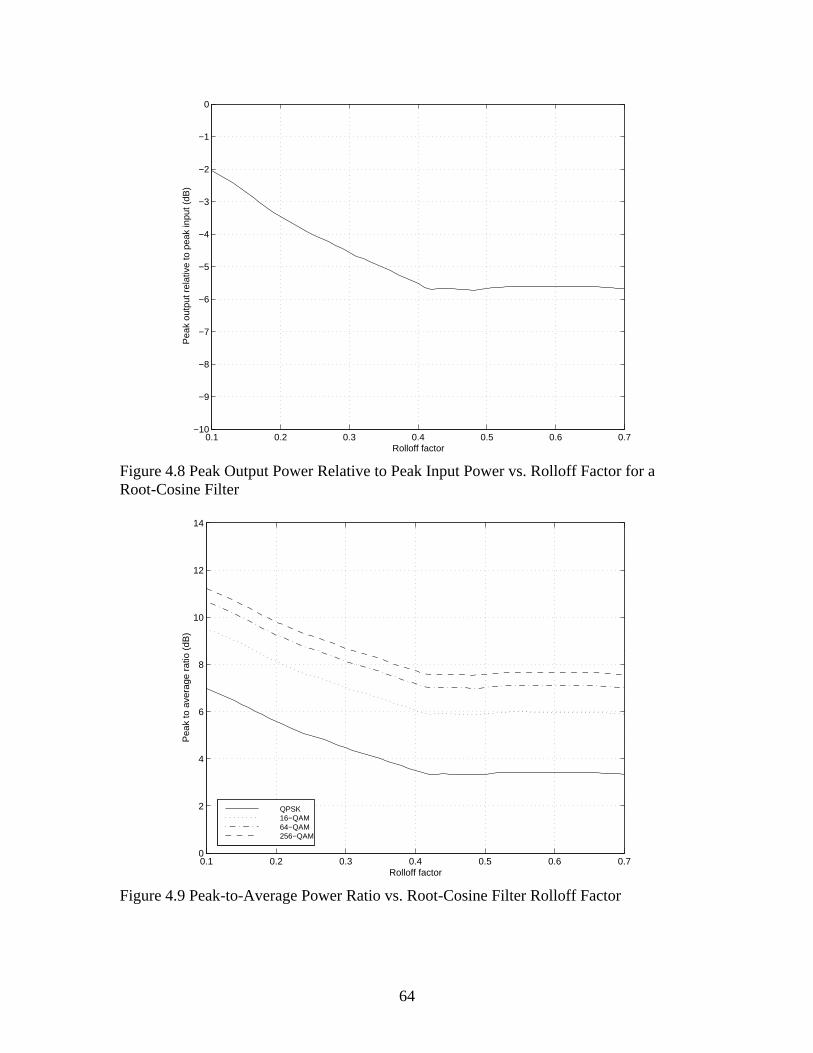
64
0.1 0.2 0.3 0.4 0.5 0.6 0.7−10
−9
−8
−7
−6
−5
−4
−3
−2
−1
0
Pea
k ou
tput
rel
ativ
e to
pea
k in
put (
dB)
Rolloff factor
Figure 4.8 Peak Output Power Relative to Peak Input Power vs. Rolloff Factor for a Root-Cosine Filter
0.1 0.2 0.3 0.4 0.5 0.6 0.70
2
4
6
8
10
12
14
Pea
k to
ave
rage
rat
io (
dB)
Rolloff factor
QPSK16−QAM64−QAM256−QAM
Figure 4.9 Peak-to-Average Power Ratio vs. Root-Cosine Filter Rolloff Factor
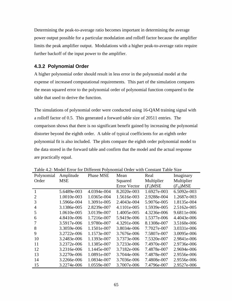
65
Determining the peak-to-average ratio becomes important in determining the average
power output possible for a particular modulation and rolloff factor because the amplifier
limits the peak amplifier output. Modulations with a higher peak-to-average ratio require
further backoff of the input power to the amplifier.
4.3.2 Polynomial Order
A higher polynomial order should result in less error in the polynomial model at the
expense of increased computational requirements. This part of the simulation compares
the mean squared error to the polynomial order of polynomial function compared to the
table that used to derive the function.
The simulations of polynomial order were conducted using 16-QAM training signal with
a rolloff factor of 0.5. This generated a forward table size of 20511 entries. The
comparison shows that there is no significant benefit gained by increasing the polynomial
distorter beyond the eighth order. A table of typical coefficients for an eighth order
polynomial fit is also included. The plots compare the eighth order polynomial model to
the data stored in the forward table and confirm that the model and the actual response
are practically equal.
Table 4.2: Model Error for Different Polynomial Order with Constant Table Size Polynomial Order
Amplitude MSE
Phase MSE Mean Squared Error Vector
Real Multiplier (FI)MSE
Imaginary Multiplier (FQ)MSE
1 5.6489e-003 4.0394e-004 8.2020e-003 1.6927e-003 6.5092e-003 2 1.0010e-003 1.0365e-004 1.5616e-003 2.9288e-004 1.2687e-003 3 1.5966e-004 1.3091e-005 2.4043e-004 5.9076e-005 1.8135e-004 4 3.1386e-005 2.8239e-007 4.1101e-005 1.5939e-005 2.5162e-005 5 1.0610e-005 3.0139e-007 1.4005e-005 4.3236e-006 9.6811e-006 6 4.8410e-006 1.7216e-007 5.9419e-006 1.5377e-006 4.4043e-006 7 3.5917e-006 1.9780e-007 4.3291e-006 8.1308e-007 3.5160e-006 8 3.3059e-006 1.1501e-007 3.8034e-006 7.7027e-007 3.0331e-006 9 3.2722e-006 1.1573e-007 3.7676e-006 7.5807e-007 3.0095e-006 10 3.2483e-006 1.1393e-007 3.7373e-006 7.5320e-007 2.9841e-006 11 3.2372e-006 1.1385e-007 3.7233e-006 7.4970e-007 2.9736e-006 12 3.2316e-006 1.1445e-007 3.7182e-006 7.4878e-007 2.9694e-006 13 3.2270e-006 1.0891e-007 3.7044e-006 7.4878e-007 2.9556e-006 14 3.2266e-006 1.0834e-007 3.7036e-006 7.4808e-007 2.9556e-006 15 3.2274e-006 1.0559e-007 3.7007e-006 7.4796e-007 2.9527e-006
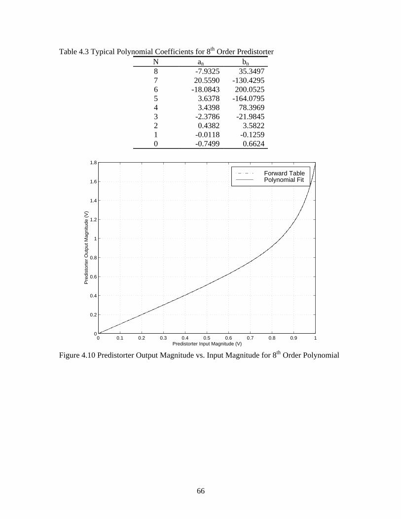
66
Table 4.3 Typical Polynomial Coefficients for 8th Order Predistorter N an bn 8 -7.9325 35.3497 7 20.5590 -130.4295 6 -18.0843 200.0525 5 3.6378 -164.0795 4 3.4398 78.3969 3 -2.3786 -21.9845 2 0.4382 3.5822 1 -0.0118 -0.1259 0 -0.7499 0.6624
0 0.1 0.2 0.3 0.4 0.5 0.6 0.7 0.8 0.9 10
0.2
0.4
0.6
0.8
1
1.2
1.4
1.6
1.8
Predistorter Input Magnitude (V)
Pre
dist
orte
r O
utpu
t Mag
nitu
de (
V)
Forward TablePolynomial Fit
Figure 4.10 Predistorter Output Magnitude vs. Input Magnitude for 8th Order Polynomial
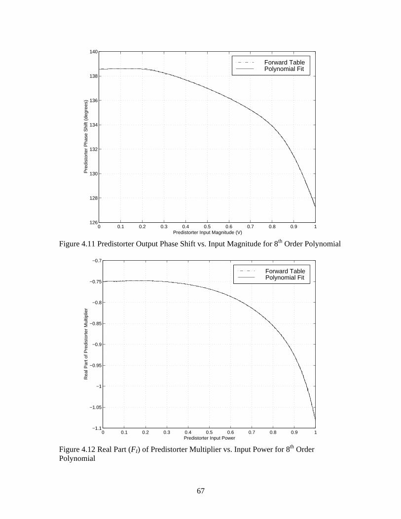
67
0 0.1 0.2 0.3 0.4 0.5 0.6 0.7 0.8 0.9 1126
128
130
132
134
136
138
140
Predistorter Input Magnitude (V)
Pre
dist
orte
r P
hase
Shi
ft (d
egre
es)
Forward TablePolynomial Fit
Figure 4.11 Predistorter Output Phase Shift vs. Input Magnitude for 8th Order Polynomial
0 0.1 0.2 0.3 0.4 0.5 0.6 0.7 0.8 0.9 1−1.1
−1.05
−1
−0.95
−0.9
−0.85
−0.8
−0.75
−0.7
Predistorter Input Power
Rea
l Par
t of P
redi
stor
ter
Mul
tiplie
r
Forward TablePolynomial Fit
Figure 4.12 Real Part (FI) of Predistorter Multiplier vs. Input Power for 8th Order Polynomial
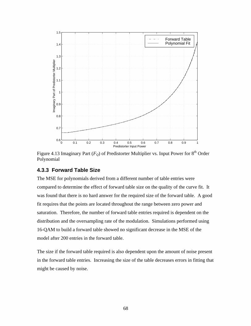
68
0 0.1 0.2 0.3 0.4 0.5 0.6 0.7 0.8 0.9 10.6
0.7
0.8
0.9
1
1.1
1.2
1.3
1.4
1.5
Predistorter Input Power
Imag
inar
y P
art o
f Pre
dist
orte
r M
ultip
lier
Forward TablePolynomial Fit
Figure 4.13 Imaginary Part (FQ) of Predistorter Multiplier vs. Input Power for 8th Order Polynomial
4.3.3 Forward Table Size
The MSE for polynomials derived from a different number of table entries were
compared to determine the effect of forward table size on the quality of the curve fit. It
was found that there is no hard answer for the required size of the forward table. A good
fit requires that the points are located throughout the range between zero power and
saturation. Therefore, the number of forward table entries required is dependent on the
distribution and the oversampling rate of the modulation. Simulations performed using
16-QAM to build a forward table showed no significant decrease in the MSE of the
model after 200 entries in the forward table.
The size if the forward table required is also dependent upon the amount of noise present
in the forward table entries. Increasing the size of the table decreases errors in fitting that
might be caused by noise.
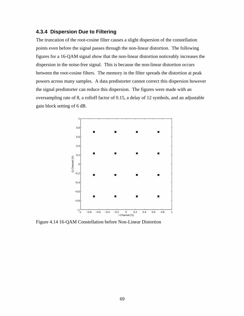
69
4.3.4 Dispersion Due to Filtering
The truncation of the root-cosine filter causes a slight dispersion of the constellation
points even before the signal passes through the non-linear distortion. The following
figures for a 16-QAM signal show that the non-linear distortion noticeably increases the
dispersion in the noise-free signal. This is because the non-linear distortion occurs
between the root-cosine filters. The memory in the filter spreads the distortion at peak
powers across many samples. A data predistorter cannot correct this dispersion however
the signal predistorter can reduce this dispersion. The figures were made with an
oversampling rate of 8, a rolloff factor of 0.15, a delay of 12 symbols, and an adjustable
gain block setting of 6 dB.
−1 −0.8 −0.6 −0.4 −0.2 0 0.2 0.4 0.6 0.8 1−1
−0.8
−0.6
−0.4
−0.2
0
0.2
0.4
0.6
0.8
1
I Channel (V)
Q C
hann
el (
V)
Figure 4.14 16-QAM Constellation before Non-Linear Distortion
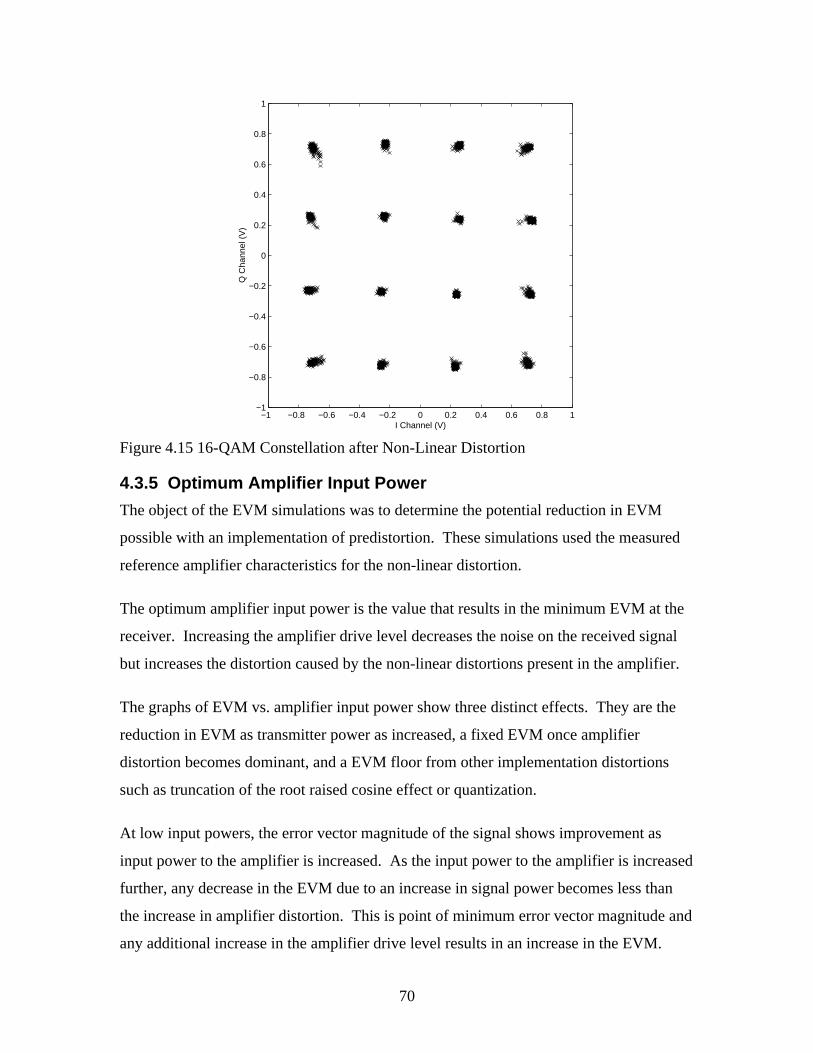
70
−1 −0.8 −0.6 −0.4 −0.2 0 0.2 0.4 0.6 0.8 1−1
−0.8
−0.6
−0.4
−0.2
0
0.2
0.4
0.6
0.8
1
I Channel (V)
Q C
hann
el (
V)
Figure 4.15 16-QAM Constellation after Non-Linear Distortion
4.3.5 Optimum Amplifier Input Power
The object of the EVM simulations was to determine the potential reduction in EVM
possible with an implementation of predistortion. These simulations used the measured
reference amplifier characteristics for the non-linear distortion.
The optimum amplifier input power is the value that results in the minimum EVM at the
receiver. Increasing the amplifier drive level decreases the noise on the received signal
but increases the distortion caused by the non-linear distortions present in the amplifier.
The graphs of EVM vs. amplifier input power show three distinct effects. They are the
reduction in EVM as transmitter power as increased, a fixed EVM once amplifier
distortion becomes dominant, and a EVM floor from other implementation distortions
such as truncation of the root raised cosine effect or quantization.
At low input powers, the error vector magnitude of the signal shows improvement as
input power to the amplifier is increased. As the input power to the amplifier is increased
further, any decrease in the EVM due to an increase in signal power becomes less than
the increase in amplifier distortion. This is point of minimum error vector magnitude and
any additional increase in the amplifier drive level results in an increase in the EVM.
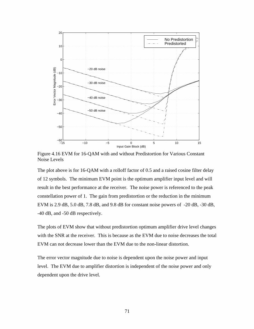
71
−15 −10 −5 0 5 10 15−60
−50
−40
−30
−20
−10
0
10
20
Input Gain Block (dB)
Err
or V
ecto
r M
agni
tude
(dB
)
−20 dB noise
−30 dB noise
−40 dB noise
−50 dB noise
No PredistortionPredistorted
Figure 4.16 EVM for 16-QAM with and without Predistortion for Various Constant Noise Levels
The plot above is for 16-QAM with a rolloff factor of 0.5 and a raised cosine filter delay
of 12 symbols. The minimum EVM point is the optimum amplifier input level and will
result in the best performance at the receiver. The noise power is referenced to the peak
constellation power of 1. The gain from predistortion or the reduction in the minimum
EVM is 2.9 dB, 5.0 dB, 7.8 dB, and 9.8 dB for constant noise powers of -20 dB, -30 dB,
-40 dB, and -50 dB respectively.
The plots of EVM show that without predistortion optimum amplifier drive level changes
with the SNR at the receiver. This is because as the EVM due to noise decreases the total
EVM can not decrease lower than the EVM due to the non-linear distortion.
The error vector magnitude due to noise is dependent upon the noise power and input
level. The EVM due to amplifier distortion is independent of the noise power and only
dependent upon the drive level.
72
Without predistortion or power control the wireless link should not be optimized for the
minimum EVM during clear weather conditions. The link should be optimized for the
minimum EVM with a SNR measured at the receiver that is just above the desired
minimum performance.
The potential gain from predistortion decreases as the constant noise power decreases if
the amplifier input is readjusted for optimum EVM. This is actually the gain of
predistortion over continuously varying the amplifier input power to achieve the
minimum EVM. If the amplifier input level remains constant, the true gain from the
implementation of predistortion remains constant as the link experiences fading. The
implementation of predistortion significantly reduces the need for varying the amplifier
input power continuously because the point of minimum EVM does not move
significantly as the SNR is decreased.
4.3.6 Adjacent Channel Power Ratio
The power spectral densities of the ideal, distorted, predistorted after amplification, and
amplified without predistortion waveforms were computed for two drive levels. The
simulated power spectral density plot has a symbol rate of 10 Msymbols/second, an
oversampling rate of 8, and a sample rate of 80 Msamples/second.
The ACPR of the predistorted signal is slightly less than the ACPR of the amplified
signal without predistortion (IQa). This difference increases with a reduction in the
backoff.
The predistorted signal has only a slightly lower ACPR than the original signal (IQm).
This confirms that this predistortion method is able to correct much of the out-of-band
interference caused by non-linear amplification and that errors in the polynomial
modeling were not severe enough to degrade the ACPR. The limiting factors to
minimizing out-of-band interference will be quantization and oversampling.
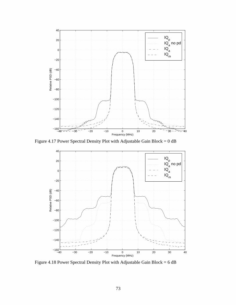
73
−40 −30 −20 −10 0 10 20 30 40−160
−140
−120
−100
−80
−60
−40
−20
0
20
40
Frequency (MHz)
Rel
ativ
e P
SD
(dB
)
IQp
IQa no pd
IQa
IQm
Figure 4.17 Power Spectral Density Plot with Adjustable Gain Block = 0 dB
−40 −30 −20 −10 0 10 20 30 40−160
−140
−120
−100
−80
−60
−40
−20
0
20
40
Frequency (MHz)
Rel
ativ
e P
SD
(dB
)
IQp
IQa no pd
IQa
IQm
Figure 4.18 Power Spectral Density Plot with Adjustable Gain Block = 6 dB
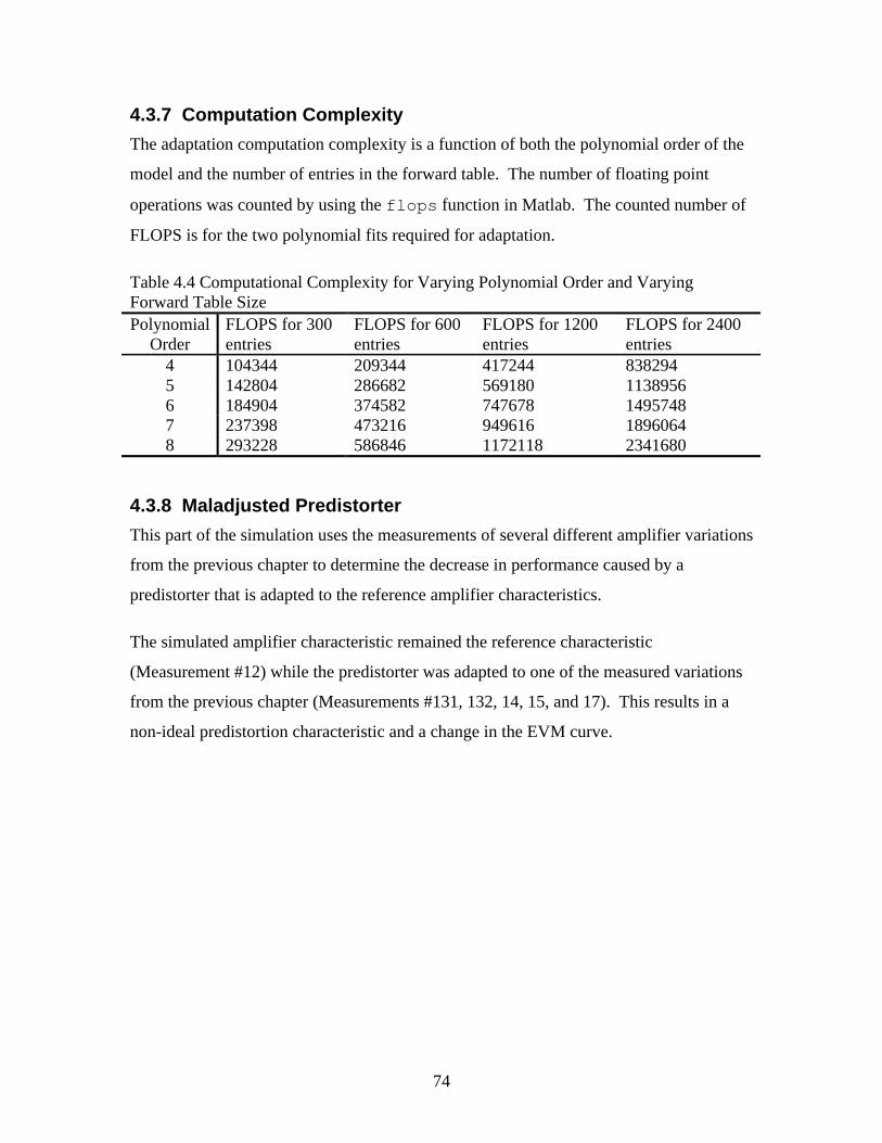
74
4.3.7 Computation Complexity
The adaptation computation complexity is a function of both the polynomial order of the
model and the number of entries in the forward table. The number of floating point
operations was counted by using the flops function in Matlab. The counted number of
FLOPS is for the two polynomial fits required for adaptation.
Table 4.4 Computational Complexity for Varying Polynomial Order and Varying Forward Table Size Polynomial
Order FLOPS for 300 entries
FLOPS for 600 entries
FLOPS for 1200 entries
FLOPS for 2400 entries
4 104344 209344 417244 838294 5 142804 286682 569180 1138956 6 184904 374582 747678 1495748 7 237398 473216 949616 1896064 8 293228 586846 1172118 2341680
4.3.8 Maladjusted Predistorter
This part of the simulation uses the measurements of several different amplifier variations
from the previous chapter to determine the decrease in performance caused by a
predistorter that is adapted to the reference amplifier characteristics.
The simulated amplifier characteristic remained the reference characteristic
(Measurement #12) while the predistorter was adapted to one of the measured variations
from the previous chapter (Measurements #131, 132, 14, 15, and 17). This results in a
non-ideal predistortion characteristic and a change in the EVM curve.

75
−15 −10 −5 0 5 10 15−40
−30
−20
−10
0
10
20
Input Gain Block (dB)
Err
or V
ecto
r M
agni
tude
(dB
)
No PredistortionCorrect27.5 GHz27.6 GHz
Figure 4.19 Maladjusted Predistorter for Different Frequencies
−15 −10 −5 0 5 10 15−40
−30
−20
−10
0
10
20
30
Input Gain Block (dB)
Err
or V
ecto
r M
agni
tude
(dB
)
No PredistortionCorrectLow V
dLow I
d
Figure 4.20 Maladjusted Predistorter for Different Bias
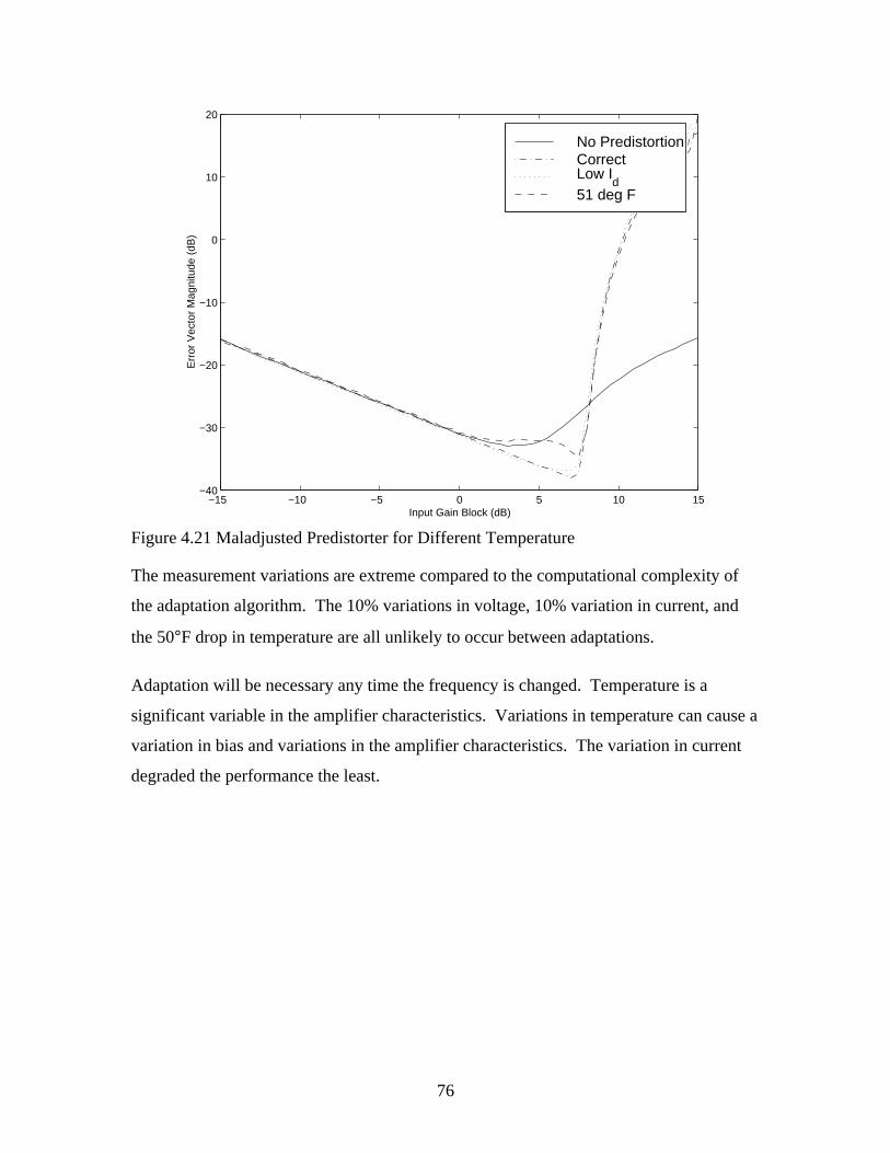
76
−15 −10 −5 0 5 10 15−40
−30
−20
−10
0
10
20
Input Gain Block (dB)
Err
or V
ecto
r M
agni
tude
(dB
)
No PredistortionCorrectLow I
d51 deg F
Figure 4.21 Maladjusted Predistorter for Different Temperature
The measurement variations are extreme compared to the computational complexity of
the adaptation algorithm. The 10% variations in voltage, 10% variation in current, and
the 50°F drop in temperature are all unlikely to occur between adaptations.
Adaptation will be necessary any time the frequency is changed. Temperature is a
significant variable in the amplifier characteristics. Variations in temperature can cause a
variation in bias and variations in the amplifier characteristics. The variation in current
degraded the performance the least.
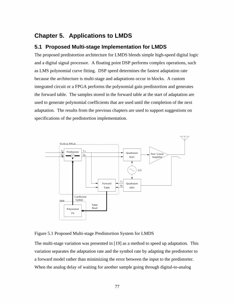
77
Chapter 5. Applications to LMDS
5.1 Proposed Multi-stage Implementation for LMDS The proposed predistortion architecture for LMDS blends simple high-speed digital logic
and a digital signal processor. A floating point DSP performs complex operations, such
as LMS polynomial curve fitting. DSP speed determines the fastest adaptation rate
because the architecture is multi-stage and adaptations occur in blocks. A custom
integrated circuit or a FPGA performs the polynomial gain predistortion and generates
the forward table. The samples stored in the forward table at the start of adaptation are
used to generate polynomial coefficients that are used until the completion of the next
adaptation. The results from the previous chapters are used to support suggestions on
specifications of the predistortion implementation.
Predistorter
Quadrature
ADC
LO
Non−LinearAmplifier
Fit
Polynomial
Q
I
Quadrature
DAC
Forward
Table
VLSI or FPGA
DSP
ReadTable
CoefficientUpdate
I
Q
I
Qm
m p
p
s
s
Figure 5.1 Proposed Multi-stage Predistortion System for LMDS
The multi-stage variation was presented in [19] as a method to speed up adaptation. This
variation separates the adaptation rate and the symbol rate by adapting the predistorter to
a forward model rather than minimizing the error between the input to the predistorter.
When the analog delay of waiting for another sample going through digital-to-analog

78
conversion, upconversion, amplification, downconversion, and analog-to-digital
conversion is eliminated, the adaptation speed is limited only by computation speed.
This separation can also be used for adaptation in systems where the sample time is less
than the computation time required for each sample. This separation also allows a typical
digital signal processor along with simple high-speed logic to be used to perform
Msymbol/second predistortion.
5.1.1 Quadrature Downconversion
Adaptive predistortion requires a feedback path. Predistortion can be preformed without
adaptation, but the simulated error vector magnitude of a maladjusted predistorter shows
that adaptation is necessary if predistortion is to achieve its potential benefits.
Multiple frequency conversions are likely necessary to convert a sample of the 28 GHz
amplifier output to a digital baseband signal. This makes the downconversion one of the
costliest parts of an implementation of adaptive digital predistortion in a LMDS system.
Using the same local oscillators as for upconversion to 28 GHz eliminates the need for
carrier synchronization in the feedback path. Time division duplex (TDD) systems have
a potential advantage because the receiver components are idle while transmitting and
could be used to sample the amplifier output.
The delay between the output of the predistorter and the corresponding sample from the
power amplifier must be adjusted within 1/64th of a symbol period [14]. Since the
oversampling rate of 8 only allows adjustment within 1/8th of a symbol period and
oversampling by 64 is not feasible, another method must be used to keep the error in the
delay minimized. The sampling clock of the analog-to-digital conversion of the amplifier
output must be delayed by a fraction of the sampling period to be able to adjust within
1/64th of a symbol period.
All predistortion implementations are sensitive to imperfections in the sampling of the
amplifier output. Utilizing a digital downconversion chip for the final downconversion to
baseband can minimize potential phase and magnitude errors. Digital downconversion
and upconversion chips are available from a several sources such as Intersil, Graychip,
and Analog Devices.
79
5.1.2 Forward Table
The forward table consists of memory and controlling logic that stores a number of
previous digital samples from the output of the predistorter and the output of the
amplifier in RAM. The forward table can be implemented with dedicated logic and
limited RAM. The logic is suitable for implementation on a custom chip or with a field
programmable gate array (FPGA). A forward table of n entries contains the previous n
samples of both signals.
Previous simulations found that forward tables larger than 300 entries did not
significantly reduce the mean squared error of the model. However, additional entries
could be added to reduce sensitivity to noise. A table size of 2400 entries is used for
evaluating computational complexity. Additional memory is required in the forward
table to delay the samples from output of the predistorter because the analog group delay
of the amplifier is longer than one symbol time.
Table indexing is not an issue since the previous samples are stored. The table of
previous samples is also necessary to verify the correct delay between the predistorted
samples and the samples of the amplifier output. This delay determination is necessary
so that the appropriate predistorter output sample is stored with the appropriate amplifier
output sample.
5.1.3 Digital Signal Processor
The digital signal processor’s primary task is to convert the information stored in the
forward table RAM into the correct polynomial predistorter coefficients to cancel the
non-linear effects of the amplifier. An additional task of the DSP is to determine the
delay between the digital sample at the output of the predistorter and the digital sample of
the amplifier output. After calculating the polynomial coefficients the DSP loads the
polynomial coefficients in the polynomial gain predistorter. These coefficients are used
until the end of the next adaptation.
The digital signal processor reads the previous samples from the forward table memory
and uses them to generate a second table called the predistorter table. The predistorter
table contains the complex predistorter multiplier as a function of the input power to the
80
predistorter block. The values in the predistorter table are obtained by dividing the
predistorter output values in the forward table by the amplifier output values in the
forward table. This inverse of the amplifier gain is then multiplied by the amplifier gain
in a low power linear region to prevent the predistorter from canceling the amplifier gain.
The result of these operations is a table of complex multipliers that will correct the
measured non-linear distortions in the amplifier. These multipliers are indexed in the
predistorter table by the linear gain divided powers of the amplifier output values in the
forward table.
A least squares fitting routine is then used to model the predistorter table as a polynomial
equation. The least square fit used in the simulation requires a floating point processor to
obtain the polynomial coefficients. The number of floating point operations (FLOPs)
was estimated in the simulation chapter. Even the worst case of adapting an eighth order
polynomial with 2400 forward table entries requires 2,341,680 floating point operations.
Under the assumption that the digital signal processor can compute 40 million floating
point operations per second (FLOPS), the time required to obtain a polynomial
approximation of the table is 0.059 seconds or about 1/17th of a second. This delay
corresponds to 585,420 symbols in the reference system of 10 Msymbols/second. A few
additional operations per table entry are required but are insignificant to the number of
operations required to obtain the polynomial coefficients.
The forward table must be filled before the coefficients can be computed. Assuming a
forward table of 2400 entries and a symbol rate of 10 Msymbols/second, the forward
table can be filled in 240 microseconds. This delay is insignificant compared to the 0.059
seconds that is required to adapt or obtain the coefficients.
The DSP also compares the both sets of samples in the forward table to generate
adjustments to the sample clock phase of the amplifier output analog-to-digital converter.
This is used to fine adjust the delay between the amplifier output and the predistorter
input within the required 1/64th of a symbol. Comparing the sign of the slope of both the
predistorter output and amplifier output signals is a method that could be used to
determine if the delay between the two inputs to the forward table are correct. If the
81
signs of the slope do not match then the delay would be adjusted in the appropriate
direction.
5.1.4 Polynomial Gain Predistorter
The proposed polynomial gain predistorter consists of two parts. The first part
implements a complex polynomial as a function of predistorter input power and the
second part is a complex multiplier. The polynomial gain predistorter can easily be
implemented in either a custom IC or a FPGA since the predistorter design contains only
multipliers and adders.
For an n order polynomial predistorter there are 62 +n real multiplications and 32 +n
real additions performed for each input sample. The proposed 8th order polynomial
predistorter requires 22 multiplications and 19 additions for each sample. This includes
conversion of the I and Q voltages samples to a power that requires 2 multiplications and
an addition. The complex multiplication of the predistortion vector with in incoming I
and Q samples requires 4 multiplications and 2 additions. For the example system with a
rate of 10 Msymbols/second with 8X oversampling for a total of 80 Msamples/second,
the computational requirement would be 3.28 GFLOPS (billion floating operations per
second). The computational needs of this predistorter are quite large when considering
implementation in a DSP but the simplicity of the calculations makes a custom IC or
FPGA implementation the best solution for the predistorter.
The structures of the multiplier and the polynomial function are shown in the figure 5.2
and figure 5.3. The notation used is the same as used when the signal predistorter is
described in the simulation chapter. I and Q are used to represent the real and imaginary
parts of a complex signal respectively. The subscript m represents the input to the
predistorter or the output from the constellation mapper, FI and FQ are the real and
imaginary outputs of the polynomial function, the subscript p represents the predistorted
signal, a and b are the real and imaginary coefficients respectively, and Xm represents the
power of the signal input to the predistorter.
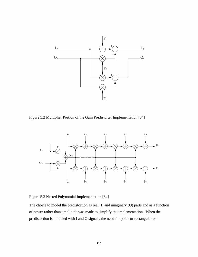
82
p
pI
Q
+
+
+
−
I
Qm
m
I
F
F
I
FQ
Figure 5.2 Multiplier Portion of the Gain Predistorter Implementation [34]
F I
FQ
bn b b b3 2 1
3 2 1na a a a a
b
0
0
I m
Qm
mX
Figure 5.3 Nested Polynomial Implementation [34]
The choice to model the predistortion as real (I) and imaginary (Q) parts and as a function
of power rather than amplitude was made to simplify the implementation. When the
predistortion is modeled with I and Q signals, the need for polar-to-rectangular or
83
rectangular-to-polar conversions is eliminated. The use of power rather than amplitude
as an input to the function eliminates the need for a square root.
5.1.5 Required Adaptation Rate
The amplifier measurements, simulation of a maladjusted predistorter, and an estimation
of the time required to compute polynomial coefficients can be used to determine the
feasibility of the proposed adaptive digital predistortion. The changes in the amplifier
characteristics for the variations were slight, but the degradation in EVM during the
amplifier variations was greater than expected. Daily adaptations to account for amplifier
aging are not sufficient and more frequent adaptations than were expected are necessary.
Repeated measurements under the same conditions and performed within several minutes
yielded similar results. It is therefore reasonable to assume that amplifier characteristics
will remain relatively static over the estimated 0.059 seconds required to compute the
polynomial coefficients. The measurement variations of 10% decreases in bias voltage,
10% decreases in bias current, and 40°F drops in temperature are unlikely to occur within
a few seconds. The reasonable times to achieve these changes are significantly longer
than the estimated adaptation time of 0.059 seconds. Therefore, this adaptation rate is
sufficient and predistortion by this method is feasible.
5.2 Implications of Predistortion for LMDS LMDS is typically a bi-directional service. Therefore, different reliabilities or different
link margins for the downstream and upstream links have no advantage. Adding
predistortion to the base station only could be used to increase the downstream data rate
while maintaining similar reliabilities for the downstream and upstream links. The
downstream data rate could be increased by an increase in the number of modulation
levels or change in forward error correction if used. Addition of predistortion to just the
base station transmitter might be useful in cost sensitive applications of predistortion. All
subscribers using that particular base station transmitter can benefit from predistortion
without the additional cost of predistortion at each subscriber. A higher downstream data
rate also better fits the demands of most subscribers.

84
If predistortion is added to both the base station and subscriber transmitters then the
system designer is given more flexibility. The gain from predistortion, like any effective
increase in transmitter power, can be used to increase antenna beamwidth, increase link
margin, increase maximum distance, increase the data rate for both upstream and
downstream links, or any combination.
The following analysis determines the potential impact of a 5 dB or 10 dB increase in the
effective transmitter power of a LMDS transmitter. This analysis is valid for any
effective increase in the transmitter power from any enhancement and is not limited to
predistortion.
The 10 dB increase in link margin allows an increase in the modulation index to the next
standard square level. The increase in data rate varies depending on the previous
modulation index. If the previous modulation were QPSK the 10 dB increase would
allow 16-QAM, which has twice the data rate for the same symbol rate, to show similar
performance. If the previous modulation were 16-QAM the 10 dB increase would allow
a 64-QAM signal to show similar performance with 1.5 times the data rate of the
16-QAM signal.
The increase in the maximum link distance is rather insignificant at short link distances.
The gains are more significant when considering lower reliability links, especially when
comparing the amount of outage minutes per year. An increase in effective power can be
used to increase the antenna beamwidth proportionally in a single dimension. This may
be desirable to reduce the number of transmitters used to cover a given area.
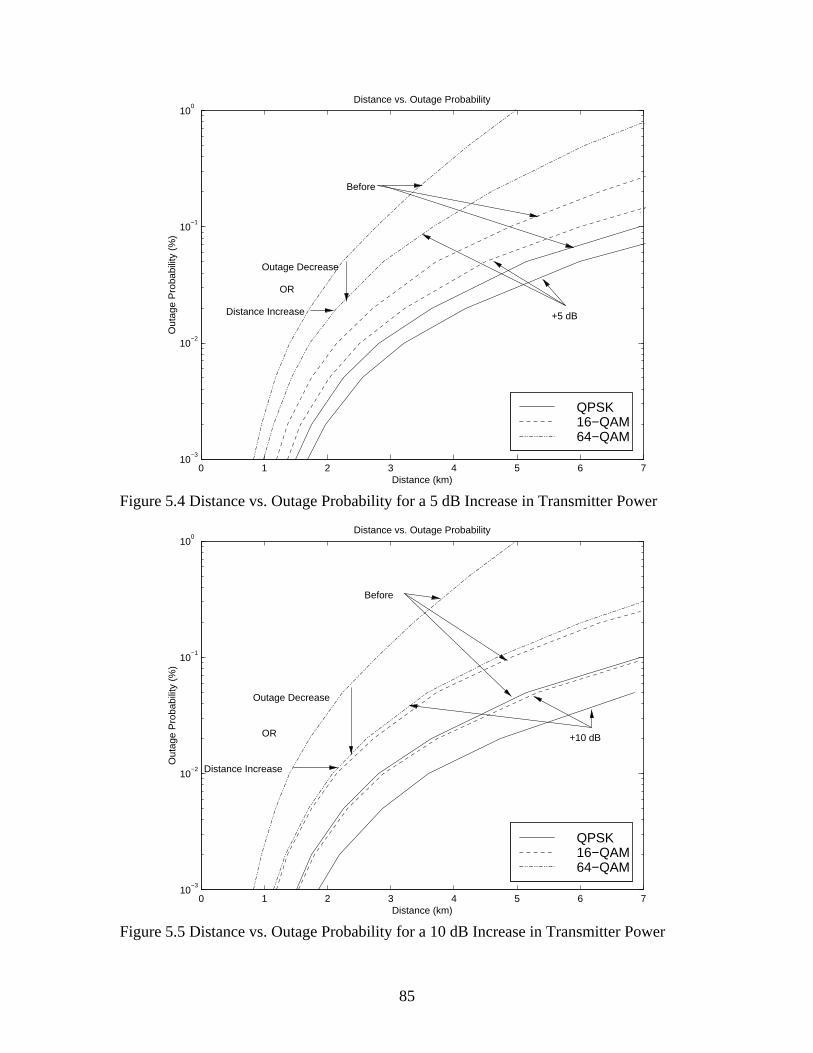
85
0 1 2 3 4 5 6 710
−3
10−2
10−1
100
Distance vs. Outage Probability
Distance (km)
Before
+5 dB
Out
age
Pro
babi
lity
(%)
Distance Increase
Outage Decrease
OR
QPSK16−QAM64−QAM
Figure 5.4 Distance vs. Outage Probability for a 5 dB Increase in Transmitter Power
0 1 2 3 4 5 6 710
−3
10−2
10−1
100
Distance vs. Outage Probability
Distance (km)
Distance Increase
Outage Decrease
OR
Out
age
Pro
babi
lity
(%)
+10 dB
Before
QPSK16−QAM64−QAM
Figure 5.5 Distance vs. Outage Probability for a 10 dB Increase in Transmitter Power
86
The implementation of predistortion in a LMDS system has other benefits. The addition
of adaptive digital predistortion can also be used to identify transmitter degradations
before total failure. The forward table or the predistorter coefficients could be
downloaded and compared with previous values to detect changes in the power amplifier.
These transmitter diagnostics are especially important in point-to-point links where it
may be difficult to identify if a link failure is due to a transmitter or the far receiver.
The typical gain for predistortion was defined as the gain between the optimum EVM
with predistortion and the optimum EVM without predistortion. The assumption was
made that the case without predistortion could be optimized. However the location of the
optimum point in unknown to a system without predistortion or EVM feedback from the
far receiver. The amplifier input power could be adjusted during the installation but it is
likely to require some additional backoff to prevent changing amplifier characteristics or
changes in the amplifier input power from degrading the EVM.
5.3 Conclusions This thesis presented a possible method for adaptive digital predistortion in LMDS
systems. Laboratory network analyzer measurements of a 28 GHz amplifier and
simulation of a digital communication system was presented to support the feasibility of
implementing predistortion in an LMDS system. An emphasis was placed on designing a
practical implementation. Predistortion at Msymbol/second rates was found to be
feasible by placing complicated adaptation algorithms in a digital signal processor,
performing simple high speed tasks with a custom IC or a FPGA, and using a multi-stage
predistortion architecture.
Adaptation to changes in the amplifier characteristics is required. The simulation showed
that even small changes in amplifier characteristics could nullify the in-band benefits of
predistortion.
The implementation of predistortion can increase the effective power of the transmitter
by as much as 10 dB. The actual increase is dependent upon level of the non-linear
distortion as compared to other distortions such as quantization, noise at the receiver, and
the peak-to-average ratio of the signal.

87
5.3.1 Future Work
The simulated amplifier model was assumed to be mostly memoryless. Two network
analyzers would be required to confirm that the amplifier time constants were negligible
at frequencies less than the simulated symbol rate. Further work might confirm that this
amplifier is memoryless at the modulation rates considered and determine its maximum
bandwidth. In addition, the effects of synchronization and equalization in the receiver
were not considered during the simulations.
A consideration of the many optimization techniques to estimate the polynomial
coefficients from a table of data points is beyond the scope of this work. Other methods
might be available that are more appropriate for fixed-point DSPs, are more efficient, or
make better use of the parallel architectures of modern DSPs.
Additional insight to implementation challenges could be gained from an actual adaptive
digital predistorter implementation. Several imperfections in the system such as
quantization, amplitude and phase errors in the quadrature conversions, and error in delay
estimation were not considered because these would be dependent upon implementation
particulars.
The measurements and simulations show that the non-linear distortion of the amplifier
cannot be ignored even in Class A amplifiers. The use of predistortion with Class AB
amplifier would enable the use of higher power amplifiers. Predistortion for an OFDM
system was not considered here but is of considerable interest because of the higher peak-
to-average power ratios of OFDM signals.

88
References
[1] Harris Corporation, Clearburst Specifications, 2000. Available: http://www.microwave.harris.com/broadband/pdf/169e.pdf.
[2] T. S. Rappaport, Wireless communications: Principles and Practice, Prentice Hall, 1996.
[3] L.J. Ippolito et al., Propagation effects handbook for satellite systems design; a summary of propagation impairments on 10 to 100 GHz satellite links with techniques for system design, NASA reference publication 1082(03), NASA 1983.
[4] W. Stutzman and Antenna theory and design, 2nd ed., Wiley, 1998.
[5] A.S. Sedra and K.C. Smith, Microelectronic circuits, Holt, Rinehart, and Winston, 3rd Edition, 1989.
[6] Cheng-Po Liang, Je-Hong Jong, W.E. Stark, J.R.East “Nonlinear amplifier effects in communications systems,” IEEE Transactions on Microwave Theory & Techniques, vol.47, no.8, Aug. 1999, pp.1461-6.
[7] J.K. Cavers. “The effect of data modulation format on intermodulation power in nonlinear amplifiers,” VTC 1994. 'Creating Tomorrow's Mobile Systems', 1994 IEEE 44th Vehicular Technology Conference, Part vol.1, 1994, pp.489-93 vol.1.
[8] W.A. Davis, Radio & Microwave Engineering, Class Notes for EE 4605, Virginia Tech, Fall 1998.
[9] H.L. Krauss, C.W. Bostian and F.H. Raab, Solid State Radio Engineering, John Wiley and Sons, 1980.
[10] S. Andreoli, H.G. McClure, P. Banelli, S. Cacopardi, “Digital linearizer for RF amplifiers,” IEEE Transactions on Broadcasting, vol.43, no.1, March 1997, pp.12-19.
[11] A. Lohtia, P.A. Goud, C.G. Englefield, “Power amplifier linearization using cubic spline interpolation,” 1993 43rd IEEE Vehicular Technology Conference. Personal Communication -Freedom Through Wireless Technology, IEEE, 1993, pp.676-9.
[12] W. Bosch and G. Gatti, “Measurement and simulation of memory effects in predistortion linearizers,” IEEE Transactions on Microwave Theory & Techniques, vol.37, no.12, Dec. 1989, pp.1885-90.
[13] K.G. Gard, H.M. Gutierrez, M.B. Steer. “Characterization of spectral regrowth in microwave amplifiers based on the nonlinear transformation of a complex Gaussian process,” IEEE Transactions on Microwave Theory & Techniques, vol.47, no.7, pt.1, July 1999, pp.1059-69.
[14] Y. Nagata, “Linear amplification technique for digital mobile communications,” 39th IEEE Vehicular Technology Conference, IEEE. 1989, pp.159-64 vol.1.
[15] B. Sklar, Digital Communications: Fundamentals and Applications, Prentice Hall, 1987.
89
[16] C. Haskins, Diode Predistortion Linearization for Power Amplifier RFICs in Digital Radios, Thesis, Virginia Polytechnic Institute and State University, 2000. Available: http://etd.vt.edu.
[17] D.J. Jennings and J.P. McGeehan, “A high-efficiency RF transmitter using VCO-derived synthesis: CALLUM,” IEEE Transactions on Microwave Theory & Techniques, vol.47, no.6, pt.1, June 1999, pp.715-21.
[18] J.K. Cavers, “A linearizing predistorter with fast adaptation,” 40th IEEE Vehicular Technology Conference. On the Move in the 90's, IEEE, 1990, pp.41-7.
[19] J.T. Stonick, V.L. Stonick, and J.M.F. Moura, “Multi-stage adaptive predistortion of HPA saturation effects for digital television transmission,” 1999 IEEE International Conference on Acoustics, Speech, and Signal Processing. Proceedings. ICASSP99, IEEE. Part vol.5, 1999, pp.2671-4 vol.5.
[20] M. Faulkner, T. Mattsson T, and W. Yates, “Adaptive linearisation using pre-distortion,” 40th IEEE Vehicular Technology Conference. On the Move in the 90's, IEEE. 1990, pp.35-40.
[21] M. Faulkner and M. Johansson, “Adaptive linearization using predistortion-experimental results,” IEEE Transactions on Vehicular Technology, vol.43, no.2, May 1994, pp.323-32.
[22] J. de Mingo J and A. Valdovinos, “Amplifier linearization using a new digital predistorter for digital mobile radio systems,” 1997 IEEE 47th Vehicular Technology Conference. Technology in Motion, IEEE, Part vol.2, 1997, pp.671-5.
[23] J.K. Cavers JK, “Optimum indexing in predistorting amplifier linearizers,” 1997 IEEE 47th Vehicular Technology Conference Technology in Motion, IEEE. Part vol.2, 1997, pp.676-80 vol.2.
[24] J.T. Stonick, V.L. Stonick, J.M.F. Moura, R.S. Zborowski, “Memoryless polynomial adaptive predistortion (TV transmitters)”, 1995 International Conference on Acoustics, Speech, and Signal Processing. Conference Proceedings, IEEE. Part vol.2, 1995, pp.981-4 vol.2.
[25] F. Szidarovszky and S. Yakowitz, Principles and procedures of numerical analysis, New York, Plenum Press, 1978.
[26] R.C. Davis and W. Boyd, “Adaptive Predistorter Technique for Linearizing a Power Amplifier for Digital Data Systems”, U.S. Patent 4,291,277, issued 22 Sept. 1982.
[27] M.E. Frerking, Digital Signal Processing in Communication Systems, Chapman & Hall, 1994.
[28] B. Taylor, private conversation and e-mail, Agilent Technologies, 2000.
[29] Agilent Technologies, “HMMC-5033 17.7-32 GHz Power Amplifier”, [Online Data Sheet], Available: http://www.semiconductor.agilent.com.
[30] Agilent Technologies, “HMMC-5040 20-40 GHz Power Amplifier”, [Online Data Sheet], Available: http://www.semiconductor.agilent.com.

90
[31] Agilent Technologies, “Controlling Test Port Output Power Flatness: PN 8510-16-A”, [Online Product Note] Available: http://www.tm.agilent.com
[32] DAVIC Standard, Part 8: Lower Layer Protocols and Phsical Interfaces, Version 1.41, Digital Audio Video Council, 2000. [Online Standard] Available: http://www.davic.org, ftp://ftp.davic.org/davic/pub/Spec1_4_1/141_part08.pdf,
[33] K. Voelker, “Apply error vector measurements in communications design,” Microwaves & RF, vol.34, no.17, Dec. 1995, pp.143-4, 146-8, 150, 152.
[34] D.S. Hilborn, S.P. Stapleton, J.K. Cavers, “An adaptive direct conversion transmitter,” IEEE Transactions on Vehicular Technology, vol.43, no.2, May 1994, pp.223-33.
[35] Wright A.S., Durtler W.G.,“Experimental performance of an adaptive digital linearized power amplifier (for cellular telephony),” IEEE Transactions on Vehicular Technology, vol.41, no.4, Nov. 1992, pp.395-400.

91
Vita
Daniel Eric Johnson was born in Tennessee on September 22, 1973. After a childhood in
Lebanon, TN, he obtained his Bachelor of Science in Electrical Engineering in 1995 from
Tennessee Technological University in Cookeville, Tennessee.
After undergraduate studies, he worked for PageNet, the world’s largest wireless
messaging provider, in Nashville, Tennessee. In 1996, he retuned to Cookeville and
worked for a small manufacturer and designer of countersurveillance equipment as an
Electrical Engineer.
In the fall of 1998, he left Tennessee to pursue a MSEE at Virginia Polytechnic Institute
and State University. His research interests included signal processing and networking
for wireless digital communications. As a part of the Center for Wireless
Telecommunications, he assisted Virginia Tech’s Communication Network Services with
the deployment of the Blacksburg LMDS Testbed System. The testbed was one of the
first licensed deployments of LMDS technology in the United States.
After completing the requirements for a Master of Science in Electrical Engineering in
the summer of 2000, Eric joined Harris Corporation’s Government Communications
Systems Division in Palm Bay, Florida.