AD7616BSTZ, AD7616, AD7616BSTZ-RL - analog.com · 16-Channel DAS with 16-Bit, Bipolar Input, Dual...
50
16-Channel DAS with 16-Bit, Bipolar Input, Dual Simultaneous Sampling ADC Data Sheet AD7616 Rev. 0 Document Feedback Information furnished by Analog Devices is believed to be accurate and reliable. However, no responsibility is assumed by Analog Devices for its use, nor for any infringements of patents or other rights of third parties that may result from its use. Specifications subject to change without notice. No license is granted by implication or otherwise under any patent or patent rights of Analog Devices. Trademarks and registered trademarks are the property of their respective owners. One Technology Way, P.O. Box 9106, Norwood, MA 02062-9106, U.S.A. Tel: 781.329.4700 ©2016 Analog Devices, Inc. All rights reserved. Technical Support www.analog.com FEATURES 16-channel, dual, simultaneously sampled inputs Independently selectable channel input ranges True bipolar: ±10 V, ±5 V, ±2.5 V Single 5 V analog supply and 2.3 V to 3.6 V V DRIVE supply Fully integrated data acquisition solution Analog input clamp protection Input buffer with 1 MΩ analog input impedance First-order antialiasing analog filter On-chip accurate reference and reference buffer Dual 16-bit successive approximation register (SAR) ADC Throughput rate: 2 × 1 MSPS Oversampling capability with digital filter Flexible sequencer with burst mode Flexible parallel/serial interface SPI/QSPI/MICROWIRE/DSP compatible Optional cyclic redundancy check (CRC) error checking Hardware/software configuration Performance 92 dB SNR at 500 kSPS (2× oversampling) 90.5 dB SNR at 1 MSPS −103 dB THD ±1 LSB INL (typical), ±0.99 LSB DNL (maximum) 8 kV ESD rating on analog input channels On-chip self detect function 80-lead LQFP package APPLICATIONS Power line monitoring Protective relays Multiphase motor control Instrumentation and control systems Data acquisition systems (DASs) GENERAL DESCRIPTION The AD7616 is a 16-bit, DAS that supports dual simultaneous sampling of 16 channels. The AD7616 operates from a single 5 V supply and can accommodate ±10 V, ±5 V, and ±2.5 V true bipolar input signals while sampling at throughput rates up to 1 MSPS per channel pair with 90.5 dB SNR. Higher SNR performance can be achieved with the on-chip oversampling mode (92 dB for an oversampling ratio (OSR) of 2). The input clamp protection circuitry can tolerate voltages up to ±21 V. The AD7616 has 1 MΩ analog input impedance, regardless of sampling frequency. The single-supply operation, on-chip filtering, and high input impedance eliminate the need for driver op amps and external bipolar supplies. The device contains analog input clamp protection, a dual, 16-bit charge redistribution SAR analog-to-digital converter (ADC), a flexible digital filter, a 2.5 V reference and reference buffer, and high speed serial and parallel interfaces. The AD7616 is serial peripheral interface (SPI)/QSPI™/DSP/ MICROWIRE compatible FUNCTIONAL BLOCK DIAGRAM Figure 1. 13591-001 R FB 1MΩ 1MΩ R FB FIRST- ORDER LPF R FB 1MΩ 1MΩ R FB FIRST- ORDER LPF V0A V0AGND R FB 1MΩ 1MΩ R FB V7A V7AGND V0B V0BGND V7B V7BGND 9:1 MUX BUSY CONVST CONTROL INPUTS CLK OSC REFINOUT REFSEL SER/PAR SER1W OSR DIGITAL FILTER 2.5V REF REFCAP NOTES 1. MULTIFUNCTION PINS, SUCH AS DB15/OS2, ARE REFERRED TO BY A SINGLE FUNCTION OF THE PIN, FOR EXAMPLE, DB15, WHEN ONLY THAT FUNCTION IS RELEVANT. REFER TO THE PIN CONFIGURATION AND FUNCTION DESCRIPTIONS SECTION FOR MORE INFORMATION. SERIAL REGCAP REGCAPD 1.8V DLDO V CC AD7616 9:1 MUX 16-BIT SAR 16-BIT SAR OS2 TO OS0 V DRIVE V CC ALDO 2:1 MUX HW_RNGSEL0, HW_RNGSEL1 CHSEL2 TO CHSEL0 SEQEN FLEXIBLE SEQUENCER BURST RESET AGND DGND DB15 TO DB0 SDOx/SDI PARALLEL FIRST- ORDER LPF R FB 1MΩ 1MΩ R FB FIRST- ORDER LPF 1.8V ALDO PARALLEL/ SERIAL INTERFACE CLAMP CLAMP CLAMP CLAMP CLAMP CLAMP CLAMP CLAMP
Transcript of AD7616BSTZ, AD7616, AD7616BSTZ-RL - analog.com · 16-Channel DAS with 16-Bit, Bipolar Input, Dual...

16-Channel DAS with 16-Bit, Bipolar Input, Dual Simultaneous Sampling ADC
Data Sheet AD7616
Rev. 0 Document Feedback Information furnished by Analog Devices is believed to be accurate and reliable. However, no responsibility is assumed by Analog Devices for its use, nor for any infringements of patents or other rights of third parties that may result from its use. Specifications subject to change without notice. No license is granted by implication or otherwise under any patent or patent rights of Analog Devices. Trademarks and registered trademarks are the property of their respective owners.
One Technology Way, P.O. Box 9106, Norwood, MA 02062-9106, U.S.A. Tel: 781.329.4700 ©2016 Analog Devices, Inc. All rights reserved. Technical Support www.analog.com
FEATURES 16-channel, dual, simultaneously sampled inputs Independently selectable channel input ranges
True bipolar: ±10 V, ±5 V, ±2.5 V Single 5 V analog supply and 2.3 V to 3.6 V VDRIVE supply Fully integrated data acquisition solution
Analog input clamp protection Input buffer with 1 MΩ analog input impedance First-order antialiasing analog filter On-chip accurate reference and reference buffer Dual 16-bit successive approximation register (SAR) ADC Throughput rate: 2 × 1 MSPS Oversampling capability with digital filter Flexible sequencer with burst mode
Flexible parallel/serial interface SPI/QSPI/MICROWIRE/DSP compatible Optional cyclic redundancy check (CRC) error checking
Hardware/software configuration Performance
92 dB SNR at 500 kSPS (2× oversampling) 90.5 dB SNR at 1 MSPS −103 dB THD ±1 LSB INL (typical), ±0.99 LSB DNL (maximum) 8 kV ESD rating on analog input channels
On-chip self detect function 80-lead LQFP package
APPLICATIONS Power line monitoring Protective relays Multiphase motor control Instrumentation and control systems Data acquisition systems (DASs)
GENERAL DESCRIPTION The AD7616 is a 16-bit, DAS that supports dual simultaneous sampling of 16 channels. The AD7616 operates from a single 5 V supply and can accommodate ±10 V, ±5 V, and ±2.5 V true bipolar input signals while sampling at throughput rates up to 1 MSPS per channel pair with 90.5 dB SNR. Higher SNR performance can be achieved with the on-chip oversampling mode (92 dB for an oversampling ratio (OSR) of 2).
The input clamp protection circuitry can tolerate voltages up to ±21 V. The AD7616 has 1 MΩ analog input impedance, regardless of sampling frequency. The single-supply operation, on-chip filtering, and high input impedance eliminate the need for driver op amps and external bipolar supplies.
The device contains analog input clamp protection, a dual, 16-bit charge redistribution SAR analog-to-digital converter (ADC), a flexible digital filter, a 2.5 V reference and reference buffer, and high speed serial and parallel interfaces.
The AD7616 is serial peripheral interface (SPI)/QSPI™/DSP/ MICROWIRE compatible
FUNCTIONAL BLOCK DIAGRAM
Figure 1.
1359
1-00
1
RFB1MΩ
1MΩ RFBFIRST-
ORDER LPF
RFB1MΩ
1MΩ RFBFIRST-
ORDER LPF
V0AV0AGND
RFB1MΩ
1MΩ RFB
V7AV7AGND
V0BV0BGND
V7BV7BGND
9:1MUX
BUSYCONVST
CONTROLINPUTS
CLK OSC
REFINOUT REFSEL
SER/PARSER1W
OSRDIGITALFILTER
2.5VREF
REFCAP
NOTES1. MULTIFUNCTION PINS, SUCH AS DB15/OS2, ARE REFERRED TO BY A SINGLE FUNCTION OF THE PIN, FOR EXAMPLE, DB15, WHEN ONLY THAT FUNCTION IS RELEVANT. REFER TO THE PIN CONFIGURATION AND FUNCTION DESCRIPTIONS SECTION FOR MORE INFORMATION.
SERIAL
REGCAP REGCAPD
1.8VDLDO
VCC
AD7616
9:1MUX
16-BITSAR
16-BITSAR
OS2 TO OS0
VDRIVE
VCC
ALDO2:1
MUX
HW_RNGSEL0, HW_RNGSEL1CHSEL2 TO CHSEL0
SEQENFLEXIBLE
SEQUENCERBURSTRESET
AGND DGND
DB15 TO DB0
SDOx/SDI
PARALLEL
FIRST-ORDER LPF
RFB1MΩ
1MΩ RFBFIRST-
ORDER LPF
1.8VALDO
PARALLEL/SERIAL
INTERFACE
CLAMPCLAMP
CLAMPCLAMP
CLAMPCLAMP
CLAMPCLAMP

AD7616 Data Sheet
Rev. 0 | Page 2 of 50
TABLE OF CONTENTS Features .............................................................................................. 1 Applications ....................................................................................... 1 General Description ......................................................................... 1 Functional Block Diagram .............................................................. 1 Revision History ............................................................................... 2 Specifications ..................................................................................... 3
Timing Specifications .................................................................. 6 Parallel Mode Timing Specifications ......................................... 8 Serial Mode Timing Specifications ............................................ 9
Absolute Maximum Ratings .......................................................... 10 Thermal Resistance .................................................................... 10 ESD Caution ................................................................................ 10
Pin Configuration and Function Descriptions ........................... 11 Typical Performance Characteristics ........................................... 15 Terminology .................................................................................... 21 Theory of Operation ...................................................................... 23
Converter Details........................................................................ 23 Analog Input ............................................................................... 23 ADC Transfer Function ............................................................. 24 Internal/External Reference ...................................................... 24 Shutdown Mode .......................................................................... 25 Digital Filter ................................................................................ 25
Applications Information .............................................................. 26 Functionality Overview ............................................................. 26
Device Configuration ..................................................................... 28 Operational Mode ...................................................................... 28 Internal/External Reference ...................................................... 28 Digital Interface .......................................................................... 28 Hardware Mode .......................................................................... 28
Software Mode ............................................................................ 29 Reset Functionality..................................................................... 29 Pin Function Overview ............................................................. 30
Digital Interface .............................................................................. 31 Channel Selection ....................................................................... 31 Parallel Interface ......................................................................... 32 Serial Interface ............................................................................ 33
Sequencer......................................................................................... 35 Hardware Mode Sequencer ....................................................... 35 Software Mode Sequencer ......................................................... 35 Burst Sequencer .......................................................................... 36
Diagnostics ...................................................................................... 38 Diagnostic Channels .................................................................. 38 Interface Self Test ....................................................................... 38 CRC .............................................................................................. 38
Register Summary .......................................................................... 40 Addressing Registers .................................................................. 41 Configuration Register .............................................................. 42 Channel Register ........................................................................ 43 Input Range Registers ................................................................ 44 Input Range Register A1............................................................ 44 Input Range Register A2............................................................ 45 Input Range Register B1 ............................................................ 46 Input Range Register B2 ............................................................ 47 Sequencer Stack Registers ......................................................... 48 Status Register ............................................................................. 49
Outline Dimensions ....................................................................... 50 Ordering Guide .......................................................................... 50
REVISION HISTORY 10/2016—Revision 0: Initial Version

Data Sheet AD7616
Rev. 0 | Page 3 of 50
SPECIFICATIONS VREF = 2.5 V external/internal, VCC = 4.75 V to 5.25 V, VDRIVE = 2.3 V to 3.6 V, fSAMPLE = 1 MSPS, TA = −40°C to +125°C, unless otherwise noted.
Table 1. Parameter Test Conditions/Comments Min Typ Max Unit DYNAMIC PERFORMANCE
Signal-to-Noise Ratio (SNR)1, 2 89 90.5 dB 92 dB 93 dB
88 89.5 dB 85.5 87 dB
Signal-to-Noise-and-Distortion (SINAD)1 88.5 90 dB 87.5 89 dB 85 87 dB
Dynamic Range 92 dB 90.5 dB 88 dB
Total Harmonic Distortion (THD)1 −103 −93.5 dB −100 dB
fIN = 1 kHz sine wave unless otherwise noted No oversampling, ±10 V range OSR = 2, ±10 V range,3 fSAMPLE = 500 kSPS OSR = 4, ±10 V range3
No oversampling, ±5 V range No oversampling, ±2.5 V range No oversampling, ±10 V range No oversampling, ±5 V range No oversampling, ±2.5 V range No oversampling, ±10 V range No oversampling, ±5 V range No oversampling, ±2.5 V range No oversampling, ±10 V range No oversampling, ±5 V range No oversampling, ±2.5 V range −97 dB
Peak Harmonic or Spurious Noise1 −103 dB Intermodulation Distortion (IMD)1 fa = 1 kHz, fb = 1.1 kHz
Second-Order Terms −105 dB Third-Order Terms −113 dB
Channel to Channel Isolation1 fIN on unselected channels up to 5 kHz −106 dB ANALOG INPUT FILTER
Full Power Bandwidth −3 dB, ±10 V range 39 kHz −3 dB, ±5 V/2.5 V range 33 kHz −0.1 dB 5.5 kHz
Phase Delay3 ±10 V range 4.4 6 μs
±5 V range 5 μs±2.5 V range 4.9 μs
Phase Delay Drift3 ±10 V range ±0.55 5 ns/°CPhase Delay Matching (Dual Simultaneous
Pair)3 ±10 V range 4.4 100 ns
±5 V range 4.7 ns±2.5 V range 4.1 ns
DC ACCURACY Resolution No missing codes 16 Bits Differential Nonlinearity (DNL)1 ±0.5 ±0.99 LSB4 Integral Nonlinearity (INL)1 ±1 ±2 LSBTotal Unadjusted Error (TUE) ±10 V range ±6 LSB
±5 V range ±8 LSB±2.5 V range ±10 LSB
Positive Full-Scale Error5
External reference ±10 V range ±5 ±32 LSB ±5 V range ± 4 LSB ±2.5 V range ± 2 LSB
Internal reference ±10 V range ±5 LSB

AD7616 Data Sheet
Rev. 0 | Page 4 of 50
Parameter Test Conditions/Comments Min Typ Max Unit Positive Full-Scale (PFS) Error Drift3 External reference ±2 ±5 ppm/°C Internal reference ±3 ±10 ppm/°C Positive Full-Scale Error Matching1 ±10 V range 3 11 LSB ±5 V range 4 LSB ±2.5 V range 8 LSB Bipolar Zero Code Error1 ±10 V range ±0.8 ±8 LSB ±5 V range ±1 ±10 LSB ±2.5 V range ±3 ±15 LSB Bipolar Zero Code Error Drift3 ±10 V range ±1.3 ±20.4 μV/°C ±5 V range ±0.9 μV/°C ±2.5 V range ±0.5 μV/°C Bipolar Zero Code Error Matching ±10 V range ±2 ±10 LSB ±5 V range ±3 LSB ±2.5 V range ±3 LSB Negative Full-Scale (NFS) Error1, 5 External reference ±10 V range ±4 ±32 LSB ±5 V range ±3 LSB ±2.5 V range ±6 LSB Internal reference ±10 V range ±3 LSB Negative Full-Scale Error Drift3 External reference ±2 ±5 ppm/°C Internal reference ±4 ppm/°C Negative Full-Scale Error Matching1 ±10 V range 4 12 LSB ±5 V range 4 LSB ±2.5 V range 8 LSB
ANALOG INPUT Input Voltage Ranges Software/hardware selectable ±10 V Software/hardware selectable ±5 V Software/hardware selectable ±2.5 V Analog Input Current ±10 V range, see Figure 34 ±10.5 μA ±5 V range, see Figure 34 ±6.5 μA ±2.5 V range, see Figure 34 ±4 μA Input Capacitance6 10 pF Input Impedance See the Analog Input section 0.85 1 MΩ Input Impedance Drift3 25 ppm/°C
REFERENCE INPUT/OUTPUT Reference Input Voltage Range See the ADC Transfer Function section 2.495 2.5 2.505 V DC Leakage Current ±1 μA Input Capacitance6 REFSEL = 1 7.5 pF Reference Output Voltage REFINOUT 2.495 2.505 V Reference Temperature Coefficient3 ±2 ±15 ppm/°C
LOGIC INPUTS Input Voltage
High (VINH) VDRIVE = 2.7 V to 3.6 V 2 V VDRIVE = 2.3 V to 2.7 V 1.7 V Low (VINL) VDRIVE = 2.7 V to 3.6 V 0.8 V VDRIVE = 2.3 V to 2.7 V 0.7 V
Input Current (IIN) ±1 μA Input Capacitance (CIN)6 5 pF

Data Sheet AD7616
Rev. 0 | Page 5 of 50
Parameter Test Conditions/Comments Min Typ Max Unit LOGIC OUTPUTS
Output Voltage High (VOH) ISOURCE = 100 μA VDRIVE − 0.2 V Low (VOL) ISINK = 100 μA 0.4 V
Floating State Leakage Current ±0.005 ±1 μA Floating State Output Capacitance6 5 pF Output Coding Twos complement
CONVERSION RATE Conversion Time Per channel pair 0.5 μs Acquisition Time Per channel pair 0.5 μs Throughput Rate Per channel pair 1 MSPS
POWER REQUIREMENTS VCC 4.75 5.25 V VDRIVE 2.3 3.6 V IVCC
Normal Mode Static 37 57 mA Operational fSAMPLE = 1 MSPS 42 65 mA
Shutdown Mode 28 μA IDRIVE Digital inputs = 0 V or VDRIVE
Normal Mode Static 0.3 0.75 mA Operational fSAMPLE = 1 MSPS 7 8 mA
Shutdown Mode 50 μA Power Dissipation
Normal Mode Static 185 300 mW Operational fSAMPLE = 1 MSPS 230 350 mW
Shutdown Mode 0.75 mW 1 See the Terminology section. 2 The user can achieve 93 dB SNR by enabling oversampling. The values are valid for manual mode. In burst mode, values degrade by ~1 dB. 3 Not production tested. Sample tested during initial release to ensure compliance. 4 LSB means least significant bit. With a ±2.5 V input range, 1 LSB = 76.293 μV. With a ±5 V input range, 1 LSB = 152.58 μV. With a ±10 V input range, 1 LSB = 305.175 μV. 5 Positive and negative full-scale error for the internal reference excludes reference errors. 6 Supported by simulation data.

AD7616 Data Sheet
Rev. 0 | Page 6 of 50
TIMING SPECIFICATIONS Universal Timing Specifications
VCC = 4.75 V to 5.25 V, VDRIVE = 2.3 V to 3.6 V, VREF = 2.5 V external reference/internal reference, TA = −40°C to +125°C, unless otherwise noted. Interface timing tested using a load capacitance of 30 pF, dependent on VDRIVE and load capacitance for serial interface (see Table 14).
Table 2. Parameter1 Min Typ Max Unit Description tCYCLE 1 µs Minimum time between consecutive CONVST rising edges (excluding burst and
oversampling modes) tCONV_LOW 50 ns CONVST low pulse width tCONV_HIGH 50 ns CONVST high pulse width tBUSY_DELAY 32 ns CONVST high to BUSY high (manual mode) tCS_SETUP 20 ns BUSY falling edge to CS falling edge setup time
tCH_SETUP 50 ns Channel select setup time in hardware mode for CHSELx tCH_HOLD 20 ns Channel select hold time in hardware mode for CHSELx tCONV 475 520 ns Conversion time for the selected channel pair tACQ 480 ns Acquisition time for the selected channel pair tQUIET 50 ns CS rising edge to next CONVST rising edge
tRESET_LOW
Partial Reset 40 500 ns Partial RESET low pulse width
Full Reset 1.2 µs Full RESET low pulse width
tDEVICE_SETUP Partial Reset 50 ns Time between partial RESET high and CONVST rising edge
Full Reset 15 ms Time between full RESET high and CONVST rising edge
tWRITE Partial Reset 50 ns Time between partial RESET high and CS for write operation
Full Reset 240 µs Time between full RESET high and CS for write operation
tRESET_WAIT 1 ms Time between stable VCC/VDRIVE and release of RESET (see Figure 50)
tRESET_SETUP Time prior to release of RESET that queried hardware inputs must be stable for (see Figure 50)
Partial Reset 10 ns Full Reset 0.05 ms
tRESET_HOLD Time after release of RESET that queried hardware inputs must be stable for (see Figure 50)
Partial Reset 10 ns Full Reset 0.24 ms
1 Not production tested. Sample tested during initial release to ensure compliance.
Figure 2. Universal Timing Diagram Across All Interfaces
CONVST
BUSY
CS
CHx yCHSEL0 TO
CHSEL2
tCYCLE
tCONV_LOW
tBUSY_DELAY
tCONV_HIGH
tQUIET
tCONV tACQ
tCS_SETUP
tCH_SETUP tCH_HOLD
HARDWAREMODE ONLY 1359
1-10
2

Data Sheet AD7616
Rev. 0 | Page 7 of 50
Figure 3. Reset Timing
VCCVDRIVE
RESET
CONVST
BUSY
CS
MODE RANGE SETTING IN HW MODE
CHx CHy CHz
ACQx CONVx ACQy CONVy
tRESET_WAIT
tDEVICE_SETUP
tWRITE
ALL MODES
HARDWAREMODE ONLY
1359
1-10
3
REFSELSER/PAR, SER1W
HW_RNGSEL0,HW_RNGSEL1
CRCEN, BURSTSEQEN, OS0 TO OS2
CHSEL0 TO CHSEL2
ADC INTERNAL ACTION
tRESET_SETUP
tRESET_HOLD
tRESET_LOW

AD7616 Data Sheet
Rev. 0 | Page 8 of 50
Parallel Mode Timing Specifications
Table 3. Parameter Min Typ Max Unit Description tRD_SETUP 10 ns CS falling edge to RD falling edge setup time
tRD_HOLD 10 ns RD rising edge to CS rising edge hold time
tRD_HIGH 10 ns RD high pulse width
tRD_LOW 30 ns RD low pulse width
tDOUT_SETUP 30 ns Data access time after falling edge of RD
tDOUT_3STATE 11 ns CS rising edge to DBx high impedance
tWR_SETUP 10 ns CS to WR setup time
tWR_HIGH 20 ns WR high pulse width
tWR_LOW 30 ns WR low pulse width
tWR_HOLD 10 ns WR hold time
tDIN_SETUP 30 ns Configuration data to WR setup time
tDIN_HOLD 10 ns Configuration data to WR hold time
tCONF_SETTLE 20 ns Configuration data settle time, WR rising edge to CONVST rising edge
Figure 4. Parallel Read Timing Diagram
Figure 5. Parallel Write Timing Diagram
CONVST
BUSY
CS
RD
CONV A CONV BDB15 TO DB0
tDOUT_3STATE
tRD_SETUP
tDOUT_SETUP 1359
1-03
3
tRD_LOW
tRD_HIGH tRD_HOLD
CONVST
CS
WR
WRITE REG 1 WRITE REG 2DB0 TODB15
tCONF_SETTLE
tWR_HIGH
tDIN_HOLD
tDIN_SETUP 1359
1-10
5
tWR_HOLD
tWR_SETUP
tWR_LOW

Data Sheet AD7616
Rev. 0 | Page 9 of 50
Serial Mode Timing Specifications
Table 4. Parameter Min Typ Max Unit Description fSCLK
1 40/50 MHz SCLK frequency tSCLK 1/fSCLK Minimum SCLK period tSCLK_SETUP
1 10.5 ns CS to SCLK falling edge setup time, VDRIVE above 3 V
13.5 ns CS to SCLK falling edge setup time, VDRIVE above 2.3 V
tSCLK_HOLD 10 ns SCLK to CS rising edge hold time
tSCLK_LOW 8 ns SCLK low pulse width tSCLK_HIGH 9 ns SCLK high pulse width tDOUT_SETUP
1 9 ns Data out access time after SCLK rising edge, VDRIVE above 3 V 11 ns Data out access time after SCLK rising edge, VDRIVE above 2.3 V tDOUT_HOLD 4 ns Data out hold time after SCLK rising edge tDIN_SETUP 10 ns Data in setup time before SCLK falling edge tDIN_HOLD 8 ns Data in hold time after SCLK falling edge tDOUT_3STATE 10 ns CS rising edge to SDOx high impedance 1 Dependent on VDRIVE and load capacitance (see Table 14).
Figure 6. Serial Timing Diagram
CONVST
BUSY
CS
1 2 3 14 15 16SCLK
DB15 DB14 DB13
DB15 DB14 DB13
DB15 DB14 DB13
DB2 DB1 DB0
DB2 DB1 DB0
DB2 DB1 DB0
SDOA
SDOB
SDI
tDOUT_SETUP tDOUT_HOLDtSCLK_SETUP
tSCLK tSCLK_HIGH
tSCLK_LOW tSCLK_HOLD
tDIN_HOLDtDIN_SETUP tDOUT_3STATE 1359
1-10
6

AD7616 Data Sheet
Rev. 0 | Page 10 of 50
ABSOLUTE MAXIMUM RATINGS TA = 25°C, unless otherwise noted.
Table 5. Parameter Rating VCC to AGND −0.3 V to +7 V VDRIVE to AGND −0.3 V to VCC + 0.3 V Analog Input Voltage to AGND1 ±21 V Digital Input Voltage to AGND −0.3 V to VDRIVE + 0.3 V Digital Output Voltage to AGND −0.3 V to VDRIVE + 0.3 V REFINOUT to AGND −0.3 V to VCC + 0.3 V Input Current to Any Pin Except
Supplies1 ±10 mA Operating Temperature Range −40°C to +125°C Storage Temperature Range −65°C to +150°C Junction Temperature 150°C Soldering Reflow
Pb/Sn Temperature (10 sec to 30 sec) 240 (+0)°C Pb-Free Temperature 260 (+0)°C
ESD All Pins Except Analog Inputs 2 kV Analog Input Pins Only 8 kV
1 Transient currents of up to 100 mA do not cause silicon controlled rectifier (SCR) latch-up.
Stresses at or above those listed under Absolute Maximum Ratings may cause permanent damage to the product. This is a stress rating only; functional operation of the product at these or any other conditions above those indicated in the operational section of this specification is not implied. Operation beyond the maximum operating conditions for extended periods may affect product reliability.
THERMAL RESISTANCE Thermal performance is directly linked to printed circuit board (PCB) design and operating environment. Close attention to PCB thermal design is required.
θJA is the natural convection junction to ambient thermal resistance measured in a one cubic foot sealed enclosure. θJC is the junction to case thermal resistance.
Table 6. Thermal Resistance Package Type θJA θJC Unit ST-80-21 41 7.5 °C/W 1 Thermal impedance simulated values are based on a JEDEC 2S2P thermal
test board. See JEDEC JESD51.
ESD CAUTION

Data Sheet AD7616
Rev. 0 | Page 11 of 50
PIN CONFIGURATION AND FUNCTION DESCRIPTIONS
Figure 7. Pin Configuration
Table 7. Pin Function Descriptions Pin No. Type1 Mnemonic2 Description 1 AI GND V4BGND Analog Input Ground Pin. This pin corresponds to Analog Input Pin V4B. 2 AI V4B Analog Input for Channel 4, ADC B. 3 AI GND V5BGND Analog Input Ground Pin. This pin corresponds to Analog Input Pin V5B. 4 AI V5B Analog Input for Channel 5, ADC B. 5, 16, 29, 72 P AGND Analog Supply Ground Pins. 6, 15, 30, 71 P VCC Analog Supply Voltage, 4.7 V to 5.25 V. This supply voltage is applied to the internal front-end
amplifiers and to the ADC core. Decouple these pins to AGND using 0.1 µF and 10 µF capacitors in parallel.
7 AI V6B Analog Input for Channel 6, ADC B. 8 AI GND V6BGND Analog Input Ground Pin. This pin corresponds to Analog Input Pin V6B. 9 AI V7B Analog Input for Channel 7, ADC B. 10 AI GND V7BGND Analog Input Ground Pin. This pin corresponds to Analog Input Pin V7B. 11 AI GND V7AGND Analog Input Ground Pin. This pin corresponds to Analog Input Pin V7A. 12 AI V7A Analog Input for Channel 7, ADC A. 13 AI GND V6AGND Analog Input Ground Pin. This pin corresponds to Analog Input Pin V6A. 14 AI V6A Analog Input for Channel 6, ADC A. 17 AI V5A Analog Input V5A. 18 AI GND V5AGND Analog Input Ground Pin. This pin corresponds to Analog Input Pin V5A. 19 AI V4A Analog Input V4A. 20 AI GND V4AGND Analog Input Ground Pin. This pin corresponds to Analog Input Pin V4A.
V4BGNDV4B
V5BGNDV5B
AGNDVCC
V6BV6BGND
V7BV7BGNDV7AGND
V7AV6AGND
V6AVCC
AGNDV5A
V5AGNDV4A
V4AGND
DB12/SDOADB13/OS0DB14/OS1DB15/OS2
DB11/SDOBDB10/SDIDB9DB8REGCAPDREGGNDDDGNDVDRIVEDB7DB6DB5/CRCEN
DB3DB2DB1DB0
V3A
GN
DV3
AV2
AG
ND
V2A
V1A
GN
DV1
AV0
AG
ND
V0A
AG
ND
V CC
REF
CA
PR
EFG
ND
REF
INO
UT
REF
INO
UTG
ND
REF
SEL
SEQ
ENH
W_R
NG
SEL1
HW
_RN
GSE
L0
V3B
GN
DV3
BV2
BG
ND
V2B
V1B
GN
DV1
BV0
BG
ND
V0B
AG
ND
V CC
REG
CA
PR
EGG
ND
CO
NVS
TB
USY
CH
SEL2
CH
SEL1
CH
SEL0
AD7616TOP VIEW
(Not to Scale)
RES
ET
SER
/PA
R
DB4/SER1W
WR
/BU
RST
SCLK
/RD
CS
2
3
4
7
6
5
1
8
9
10
12
13
14
15
16
17
18
19
20
11
59
58
57
54
55
56
60
53
52
51
49
48
47
46
45
44
43
42
41
50
21 22 23 24 25 26 27 28 29 30 31 32 33 34 35 36 37 38 39 40
80 79 78 77 76 75 74 73 72 71 70 69 68 67 66 65 64 63 62 61
ANALOG INPUT
DECOUPLING CAP PIN
POWER SUPPLY
GROUND PIN
DIGITAL INPUT
REFERENCE INPUT/OUTPUT
DIGITAL INPUT/OUTPUT
DIGITAL OUTPUT 1359
1-00
5

AD7616 Data Sheet
Rev. 0 | Page 12 of 50
Pin No. Type1 Mnemonic2 Description 21 AI GND V3AGND Analog Input Ground Pin. This pin corresponds to Analog Input Pin V3A. 22 AI V3A Analog Input for Channel 3, ADC A. 23 AI GND V2AGND Analog Input Ground Pin. This pin corresponds to Analog Input Pin V2A. 24 AI V2A Analog Input for Channel 2, ADC A. 25 AI GND V1AGND Analog Input Ground Pin. This pin corresponds to Analog Input Pin V1A. 26 AI V1A Analog Input for Channel 1, ADC A. 27 AI GND V0AGND Analog Input Ground Pin. This pin corresponds to Analog Input Pin V0A. 28 AI V0A Analog Input for Channel 0, ADC A. 31 CAP REFCAP Reference Buffer Output Force/Sense Pin. Decouple this pin to AGND using a low effective
series resistance (ESR), 10 µF, X5R ceramic capacitor, as close to the REFCAP pin as possible. The voltage on this pin is typically 4.096 V.
32 CAP REFGND Reference Ground pin. Connect this pin to AGND. 33 REF REFINOUT Reference Input/Reference Output. The on-chip reference of 2.5 V is available on this pin for
external use when the REFSEL pin is set to logic high. Alternatively, the internal reference can be disabled by setting the REFSEL pin to logic low, and an external reference of 2.5 V can be applied to this input. Decoupling is required on this pin for both the internal and external reference options. Connect a 100 nF, X8R capacitor between the REFINOUT and REFINOUTGND pins, as close to the REFINOUT pin as possible. If using an external reference, connect a 10 kΩ series resistor to this pin to band limit the reference signal.
34 CAP REFINOUTGND Reference Input, Reference Output Ground Pin. 35 DI REFSEL Internal/External Reference Selection Input. REFSEL is a logic input. If this pin is set to logic
high, the internal reference is selected and enabled. If this pin is set to logic low, the internal reference is disabled and an external reference voltage must be applied to the REFINOUT pin. The signal state is latched on the release of a full reset, and requires an additional full reset to reconfigure.
36 DI RESET Reset Input. Full and partial reset options are available. The type of reset is determined by the length of the RESET pulse. Keeping RESET low places the device into shutdown mode. See the Reset Functionality section for further details.
37 DI SEQEN Channel Sequencer Enable Input (Hardware Mode Only). When SEQEN is tied low, the sequencer is disabled.
When SEQEN is high, the sequencer is enabled (with restricted functionality in hardware mode). See the Sequencer section for further details. The signal state is latched on the release of a full reset, and requires an additional full reset to reconfigure.
In software mode, this pin must be connected to DGND. 38, 39 DI HW_RNGSEL1,
HW_RNGSEL0 Hardware/Software Mode Selection, Hardware Mode Range Select Inputs. Hardware/software mode selection is latched at full reset. Range selection in hardware mode is not latched.
HW_RNGSELx = 00: software mode; the AD7616 is configured via the software registers. HW_RNGSELx = 01: hardware mode; analog input range is ±2.5 V. HW_RNGSELx = 10: hardware mode; analog input range is ±5 V. HW_RNGSELx = 11: hardware mode; analog input range is ±10 V. 40 DI SER/PAR Serial/Parallel Interface Selection Input. Logic input. If this pin is tied to a logic low, the parallel
interface is selected. If this pin is tied to logic high, the serial interface is selected. The signal state is latched on the release of a full reset, and requires an additional full reset to reconfigure.
41, 42, 43, 44
DO/DI DB0, DB1, DB2, DB3
Parallel Output/Input Data Bit 0 to Data Bit 3. In parallel mode, these pins are output/input parallel data bits, DB7 to DB0. Refer to the Parallel Interface section for further details. In serial mode, these pins must be tied to DGND.
45 DO/DI DB4/SER1W Parallel Output/Input Data Bit 4/Serial Output Selection. In parallel mode, this pin acts as a three-state parallel digital output/input pin. Refer to the Parallel Interface section for further details.
In serial mode, this pin determines whether the serial output operates over SDOA and SDOB or just SDOA. When SER1W is low, the serial output operates over SDOA only. When SER1W is high, the serial output operates over both SDOA and SDOB. The signal state is latched on the release of a full reset, and requires an additional full reset to reconfigure.

Data Sheet AD7616
Rev. 0 | Page 13 of 50
Pin No. Type1 Mnemonic2 Description 46 DO/DI DB5/CRCEN Parallel Output/Input Data Bit 5/CRC Enable Input. In parallel mode, this pin acts as a three-
state parallel digital input/output. While in serial mode, this pin acts as a CRC enable input. The CRCEN signal state is latched on the release of a full reset, and requires an additional full reset to reconfigure. Refer to the Digital Interface section for further details.
In serial mode, when CRCEN is low, there is no CRC word following the conversion results; when CRCEN is high, an extra CRC word follows the last conversion word configured by CHSELx. See the CRC section for further details.
In software mode, this pin must be connected to DGND. 47, 48 DO/DI DB6, DB7 Parallel Output/Input Data Bit 6 and Data Bit 7. When SER/PAR = 0, these pins act as three-
state parallel digital input/outputs. Refer to the Parallel Interface section for further details. In serial mode, when SER/PAR = 1 these pins must be tied to DGND.
49 P VDRIVE Logic Power Supply Input. The voltage (2.3 V to 3.6 V) supplied at this pin determines the operating voltage of the interface. This pin is nominally at the same supply as the supply of the host interface. Decouple this pin with 0.1 µF and 10 µF capacitors in parallel.
50 P DGND Digital Ground. This pin is the ground reference point for all digital circuitry on the AD7616. The DGND pin must connect to the DGND plane of a system.
51 CAP REGGNDD Ground for the Digital Low Dropout (LDO) Regulator Connected to REGCAPD (Pin 52). 52 CAP REGCAPD Decoupling Capacitor Pin for Voltage Output from Internal Digital Regulator. Decouple this
output pin separately to REGGNDD using a 10 μF capacitor. The voltage at this pin is 1.89 V typical. 53, 54 DO/DI DB8, DB9 Parallel Output/Input Data Bit 9 and Data Bit 8. When SER/PAR = 0, these pins act as three-
state parallel digital input/outputs. Refer to the Parallel Interface section for further details. In serial mode, when SER/PAR = 1, these pins must be tied to DGND.
55 DO/DI DB10/SDI Parallel Output/Input Data Bit DB10/Serial Data Input. When SER/PAR = 0, this pin acts as a three-state parallel digital input/output. Refer to the Parallel Interface section for further details. In hardware serial mode, tie this pin to DGND.
In serial mode, when SER/PAR = 1, this pin acts as the data input of the SPI interface.
56 DO/DI DB11/SDOB Parallel Output/Input Data Bit 11/Serial Data Output B. When SER/PAR = 0, this pin acts as a three-state parallel digital input/output. Refer to the Parallel Interface section for further details.
In serial mode, when SER/PAR = 1, this pin functions as SDOB and outputs serial conversion data.
57 DO/DI DB12/SDOA Parallel Output/Input Data Bit 12/Serial Data Output A. When SER/PAR = 0, this pin acts as a three-state parallel digital input/output. Refer to the Parallel Interface section for further details.
In serial mode, when SER/PAR = 1, this pin functions as SDOA and outputs serial conversion data.
58, 59, 60 DO/DI DB13/OS0, DB14/OS1, DB15/OS2
Parallel Output/Input Data Bit 13, Data Bit 14, and Data Bit 15/Oversampling Ratio Selection. When SER/PAR = 0, these pins act as three-state parallel digital input/outputs. Refer to the Parallel Interface section for further details.
In serial hardware mode, these pins control the oversampling settings. The signal state is latched on the release of a full reset, and requires an additional full reset to reconfigure. See the Digital Filter section for further details.
In software serial mode, these pins must be connected to DGND. 61 DI WR/BURST Write/Burst Mode Enable.
In software parallel mode, this pin acts as WR for a parallel interface.
In hardware parallel or serial mode, this pin enables BURST mode. The signal state is latched on the release of a full reset, and requires an additional full reset to reconfigure. Refer to the Burst Sequencer section for further information.
In software serial mode, connect this pin to DGND. 62 DI SCLK/RD Serial Clock Input/Parallel Data Read Control Input. In serial mode, this pin acts as the serial
clock input for data transfers. The CS falling edge takes the SDOA and SDOB data output lines out of three-state and clocks out the MSB of the conversion result. The rising edge of SCLK clocks all subsequent data bits onto the SDOA and SDOB serial data outputs.
When both CS and RD are logic low in parallel mode, the output bus is enabled.
63 DI CS Chip Select. This active low logic input frames the data transfer.
In parallel mode, when both CS and RD are logic low, the DBx output bus is enabled and the conversion result is output on the parallel data bus lines.
In serial mode, CS frames the serial read transfer and clocks out the MSB of the serial output data.

AD7616 Data Sheet
Rev. 0 | Page 14 of 50
Pin No. Type1 Mnemonic2 Description 64, 65, 66 DI CHSEL0, CHSEL1,
CHSEL2 Channel Selection Input 0 to Input 2. In hardware mode, these inputs select the input channels for the next conversion in Channel Group A and Channel Group B. For example, CHSELx = 0x000 selects V0A and V0B for the next conversion; CHSELx = 0x001 selects V1A and V1B for the next conversion.
In software mode, these pins must be connected to DGND. 67 DO BUSY Busy Output. This pin transitions to a logic high after a CONVST rising edge and indicates that
the conversion process has started. The BUSY output remains high until the conversion process for the current selected channels is complete. The falling edge of BUSY signals that the conversion data is being latched into the output data registers and is available to read. Data must be read after BUSY returns to low. Rising edges on CONVST have no effect while the BUSY signal is high.
68 DI CONVST Conversion Start Input for Channel Group A and Channel Group B. This logic input initiates conversions on the analog input channels.
A conversion is initiated when CONVST transitions from low to high for the selected analog input pair. When burst mode and oversampling mode are disabled, every CONVST transition from low to high converts one channel pair. In sequencer mode, when burst mode or oversampling is enabled, a single CONVST transition from low to high is necessary to perform the required number of conversions.
69 CAP REGGND Internal Analog Regulator Ground. This pin must connect to the AGND plane of a system. 70 CAP REGCAP Decoupling Capacitor Pin for Voltage Output from Internal Analog Regulator. Decouple this
output pin separately to REGGND using a 10 μF capacitor. The voltage at this pin is 1.87 V typical.
73 AI V0B Analog Input for Channel 0, ADC B. 74 AI GND V0BGND Analog Input Ground Pin. This pin corresponds to Analog Input Pin V0B. 75 AI V1B Analog Input for Channel 1, ADC B. 76 AI GND V1BGND Analog Input Ground Pin. This pin corresponds to Analog Input Pin V1B. 77 AI V2B Analog Input for Channel 2, ADC B. 78 AI GND V2BGND Analog Input Ground Pin. This pin corresponds to Analog Input Pin V2B. 79 AI V3B Analog Input for Channel 3, ADC B. 80 AI GND V3BGND Analog Input Ground Pin. This pin corresponds to Analog Input Pin V3B. 1 AI is analog input, GND is ground, P is power supply, REF is reference input/output, DI is digital input, DO is digital output, and CAP is decoupling capacitor pin. 2 Note that throughout this data sheet, multifunction pins, such as SER/PAR, are referred to either by the entire pin name or by a single function of the pin, for example,
SER, when only that function is relevant.

Data Sheet AD7616
Rev. 0 | Page 15 of 50
TYPICAL PERFORMANCE CHARACTERISTICS VREF = 2.5 V internal, VCC = 5 V, VDRIVE = 3.3 V, fSAMPLE = 1 MSPS, fIN = 1 kHz TA = 25°C, unless otherwise noted.
Figure 8. Fast Fourier Transform (FFT), ±10 V Range
Figure 9. FFT, ±5 V Range
Figure 10. FFT Burst Mode, ±10 V Range
Figure 11. SNR vs. Temperature
Figure 12. SINAD vs. Temperature
Figure 13. THD vs. Temperature
–160
–140
–120
–100
–80
–60
–40
–20
0
200 40 60 80 100
MA
GN
ITU
DE
(dB
)
FREQUENCY (kHz) 1359
1-20
8
SNR = 90.44dBSINAD = 90.25dBTHD = –103.41dBN SAMPLES = 65536
–160
–140
–120
–100
–80
–60
–40
–20
0
200 40 60 80 100
MA
GN
ITU
DE
(dB
)
FREQUENCY (kHz)
SNR = 89.59dBSINAD = 89.39dBTHD = –102.36dBN SAMPLES = 65536
1359
1-20
9
–160
–140
–120
–100
–80
–60
–40
–20
0
100 20 30 40 50
MA
GN
ITU
DE
(dB
)
FREQUENCY (kHz)
SNR = 90.6dBSINAD = 90.65dBTHD = –107.4dBN SAMPLES = 65536
1359
1-21
0
80
82
84
86
88
90
92
94
96
98
100
–40 –25 –10 5 20 35 50 65 80 95 110 125
SNR
(dB
)
TEMPERATURE (°C)
±10V RANGE±5V RANGE±2.5V RANGE
1359
1-21
1
80
82
84
86
88
90
92
94
96
98
100
–40 –25 –10 5 20 35 50 65 80 95 110 125
SIN
AD
(dB
)
TEMPERATURE (°C)
±10V RANGE±5V RANGE±2.5V RANGE
1359
1-21
2
–120
–110
–100
–90
–80
–70
–60
–40 –25 –10 5 20 35 50 65 80 95 110 125
THD
(dB
)
TEMPERATURE (°C)
RSOURCE MATCHED ON Vx AND VxGND INPUTS
±10V RANGE±5V RANGE±2.5V RANGE
1359
1-21
3

AD7616 Data Sheet
Rev. 0 | Page 16 of 50
Figure 14. Typical INL Error, ±10 V Range
Figure 15. Typical INL Error, ±5 V Range
Figure 16. Typical DNL Error, ±10 V Range
Figure 17. Typical DNL Error, ±5 V Range
Figure 18. DC Histogram of Codes at Code Center, ±10 V Range
Figure 19. DC Histogram of Codes at Code Center, ±5 V Range
0 10000 20000 30000 40000 50000 60000
INL
ERR
OR
(LSB
)
CODE 1359
1-21
4–2.0
–1.5
–1.0
–0.5
0
0.5
1.0
1.5
2.0
0 10000 20000 30000 40000 50000 60000
INL
ERR
OR
(LSB
)
CODE 1359
1-21
5–2.0
–1.5
–1.0
–0.5
0
0.5
1.0
1.5
2.0
0 10000 20000 30000 40000 50000 60000
DN
L ER
RO
R (L
SB)
CODE 1359
1-21
6–2.0
–1.5
–1.0
–0.5
0
0.5
1.0
1.5
2.0
0 10000 20000 30000 40000 50000 60000
CODE 1359
1-21
7
DN
L ER
RO
R (L
SB)
–2.0
–1.5
–1.0
–0.5
0
0.5
1.0
1.5
2.0
29
32731
26334
229750
5000
10000
15000
20000
25000
30000
35000
32766 32767 32768 32769 32770 32771
NU
MB
ER O
F H
ITS
CODE
±10V RANGEVxx AND VxxGNDSHORTED TOGETHER65536 SAMPLES
4140
1359
1-21
8
363021
24343
31138
6841
1570
5000
10000
15000
20000
25000
30000
35000
32764 32765 32766 32767 32768 32769
NU
MB
ER O
F H
ITS
CODE
±5V RANGEVxx AND VxxGNDSHORTED TOGETHER65536 SAMPLES
1359
1-21
9

Data Sheet AD7616
Rev. 0 | Page 17 of 50
Figure 20. DC Histogram of Codes at Code Center, ±2.5 V Range
Figure 21. NFS Error vs. Temperature
Figure 22. PFS Error vs. Temperature
Figure 23. PFS/NFS Error vs. Source Resistance
Figure 24. NFS/PFS Error Matching vs. Temperature
Figure 25. Bipolar Zero Code Error vs. Temperature
1 85
2022
13596
27621
18123
249 2 10
5000
10000
15000
20000
25000
30000
32757 32758 32759 32760 32761 32762 32763 32764 32765 32768
NU
MB
ER O
F H
ITS
CODE
±2.5V RANGEVxx and VxxGNDSHORTED TOGETHER65536 SAMPLES
3836
1359
1-22
0
–30
–20
–10
0
10
20
30
–40 –25 –10 5 20 35 50 65 80 95 110 125
NFS
ER
RO
R (L
SB)
TEMPERATURE (°C)
±10V RANGE±5V RANGE±2.5V RANGE
1359
1-22
1
–30
–20
–10
0
10
20
30
–40 –25 –10 5 20 35 50 65 80 95 110 125
PFS
ERR
OR
(LSB
)
TEMPERATURE (°C)
±10V RANGE±5V RANGE±2.5V RANGE
1359
1-22
2
0
0.001
0.002
0.003
0.004
0.005
0.006
0.007
0.008
0.009
0 20 40 60 80 100
1359
1-22
3
PFS/
NFS
ERR
OR
(%FS
)
SOURCE RESISTANCE (kΩ)
NFS ±10V RANGENFS ±5V RANGENFS ±2.5V RANGEPFS ±10V RANGEPFS ±5V RANGEPFS ±2.5V RANGE
–40 –25 –10 5 20 35 50 65 80 95 110 125
TEMPERATURE (°C)
0
1
2
3
4
5
6
7
8
9
10
NFS
/PFS
ER
RO
R M
ATC
HIN
G (L
SB)
PFS ±10V RANGENFS ±10V RANGE
1359
1-22
4
-10
-8
-6
-4
-2
0
2
4
6
8
10
BIP
OLA
R Z
ERO
CO
DE
ERR
OR
(LSB
)
–40 –25 –10 5 20 35 50 65 80 95 110 125
TEMPERATURE (°C)
±10V RANGE±5V RANGE±2.5V RANGE
1359
1-22
5

AD7616 Data Sheet
Rev. 0 | Page 18 of 50
Figure 26. Bipolar Zero Error Matching vs. Temperature
Figure 27. THD vs. Input Frequency for Various Source Impedances,
±10 V Range
Figure 28. THD vs. Input Frequency for Various Source
Impedances, ±5 V Range
Figure 29. SNR vs. Input Frequency for Different Oversampling Rates, ±10 V Range
Figure 30. SNR vs. Input Frequency for Different Oversampling Rates,
±5 V Range
Figure 31. Channel to Channel Isolation
0
1
2
3
4
5
6
7
8
–40 –25 –10 5 20 35 50 65 80 95 110 125
BIP
OLA
R Z
ERO
ER
RO
R M
ATC
HIN
G (L
SB)
TEMPERATURE (°C)
DC INPUT
1359
1-22
6
±10V RANGE±5V RANGE±2.5V RANGE
–110
–100
–90
–80
–70
–60
–50
–40
1k 10k 100k
THD
(dB
)
INPUT FREQUENCY (Hz)
0Ω50Ω100Ω1.2kΩ5.6kΩ10kΩ23.7kΩ47.3kΩ105kΩ
1359
1-22
7
±10V RANGERSOURCE MATCHED ON Vxx AND VxxGND INPUTS
–120
–110
–100
–90
–80
–70
–60
–50
–40
1k 10k 100k
THD
(dB
)
INPUT FREQUENCY (Hz)
0Ω50Ω100Ω1.2kΩ5.6kΩ10kΩ23.7kΩ47.3kΩ105kΩ
1359
1-22
8
±5V RANGERSOURCE MATCHED ON Vxx AND VxxGND INPUTS
100 1k 10k 100k
SNR
(dB
)
INPUT FREQUENCY (Hz)
NO OSOSR × 2OSR × 4OSR × 8OSR × 16OSR × 32
80
82
84
86
88
90
92
94
96
98
1359
1-22
9
±10V RANGE
100 1k 10k 100k
SNR
(dB
)
INPUT FREQUENCY (Hz)
NO OSOSR × 2OSR × 4OSR × 8OSR × 16OSR × 32
80
82
84
86
88
90
92
94
96
98
1359
1-23
0
±5V RANGE
–150
–140
–130
–120
–110
–100
–90
–80
–70
–60
–50
0 5000 10000 15000 20000 25000 30000
CH
AN
NE
LTO
CH
AN
NE
L IS
OLA
TIO
N (d
B)
INTERFERER FREQUENCY (Hz)
±10V RANGE±5V RANGE±2.5V RANGE
1359
1-23
1

Data Sheet AD7616
Rev. 0 | Page 19 of 50
Figure 32. Phase Delay vs. Temperature
Figure 33. Internal Reference Voltage vs. Temperature for Various
Supply Voltages
Figure 34. Analog Input Current vs. Temperature for Various Supply Voltages
Figure 35. PSRR vs. Ripple Frequency
Figure 36. CMRR vs. Ripple Frequency
Figure 37. Static/Dynamic IVCC Current vs. Temperature
0
2
4
6
8
10
12
–40 –25 –10 5 20 35 50 65 80 95 110 125
PHA
SED
ELA
Y(µ
s)
TEMPERATURE (°C)
±10V RANGE±5V RANGE±2.5V RANGE
1359
1-23
2
2.490
2.495
2.500
2.505
2.510
–40 –25 –10 5 20 35 50 65 80 95 110 125
INTE
RN
AL
REF
EREN
CE
VOLT
AG
E (V
)
TEMPERATURE (°C)
4.75V5V5.25V
1359
1-23
4
–15
–10
–5
0
5
10
15
–40 –25 –10 5 20 35 50 65 80 95 110 125
AN
ALO
G IN
PUT
CU
RR
ENT
(µA
)
TEMPERATURE (°C)
+10V INPUT
–10V INPUT
+5V INPUT
–5V INPUT
+2.5V INPUT
–2.5V INPUT
1359
1-23
5
40
50
60
70
80
90
100
110
120
130
0.1 1 10 100 1000
PSR
R (d
B)
RIPPLE FREQUENCY (kHz)
±10V RANGE±5V RANGE±2.5V RANGE
100mV p-p SINE WAVEAPPLIED TO VCC SUPPLY
1359
1-23
6
–120
–100
–80
–60
–40
–20
0
10 100 1k 10k 100k 1M 10M
CM
RR
(dB
)
RIPPLE FREQUENCY (Hz)
±10V RANGE±5V RANGE±2.5V RANGE
1359
1-23
7
0
10
20
30
40
50
60
70
80
90
100
–40 –25 –10 5 20 35 50 65 80 95 110 125TEMPERATURE (°C)
STA
TIC
/DYN
AM
IC IV
CC
CU
RR
ENT
(mA
)
1359
1-23
8
STATIC
DYNAMIC

AD7616 Data Sheet
Rev. 0 | Page 20 of 50
Figure 38. Dynamic VDRIVE Current vs. Temperature
Figure 39. Static VDRIVE Current vs. Temperature
Figure 40. IVCC Current vs. Sampling Frequency
0
0.5
1.0
1.5
2.0
2.5
3.0
3.5
4.0
4.5
5.0
DYN
AM
IC V
DR
IVE
CU
RR
ENT
(mA
)
TEMPERATURE (°C)
–40 –25 –10 5 20 35 50 65 80 95 110 125
1359
1-23
9
0
0.1
0.2
0.3
0.4
0.5
0.6
0.7
STA
TIC
VD
RIV
E C
UR
REN
T (m
A)
–40 –25 –10 5 20 35 50 65 80 95 110 125TEMPERATURE (°C) 13
591-
240
38
39
40
41
42
43
44
45
46
47
100 200 300 400 500 600 700 800 900 1000
I VC
C C
UR
REN
T (m
A)
SAMPLING FREQUENCY (kSPS) 1359
1-24
1

Data Sheet AD7616
Rev. 0 | Page 21 of 50
TERMINOLOGY Integral Nonlinearity (INL) INL is the maximum deviation from a straight line passing through the endpoints of the ADC transfer function. The endpoints of the transfer function are zero scale, at ½ LSB below the first code transition; and full scale, at ½ LSB above the last code transition.
Differential Nonlinearity (DNL) DNL is the difference between the measured and the ideal 1 LSB change between any two adjacent codes in the ADC.
Bipolar Zero Code Error Bipolar zero code error is the deviation of the midscale transition (all 1s to all 0s) from the ideal, which is 0 V − ½ LSB.
Bipolar Zero Code Error Matching Bipolar zero code error matching is the absolute difference in bipolar zero code error between any two input channels.
Positive Full-Scale (PFS) Error Positive full-scale error is the deviation of the actual last code transition from the ideal last code transition (10 V − 1½ LSB (9.99954), 5 V − 1½ LSB (4.99977) and 2.5 V − 1½ LSB (2.49989)) after bipolar zero code error is adjusted out. The positive full-scale error includes the contribution from the internal reference buffer.
Positive Full-Scale Error Matching Positive full-scale error matching is the absolute difference in positive full-scale error between any two input channels.
Negative Full-Scale (NFS) Error Negative full-scale error is the deviation of the first code transition from the ideal first code transition (−10 V + ½ LSB (−9.99985), −5 V + ½ LSB (−4.99992) and −2.5 V + ½ LSB (−2.49996)) after the bipolar zero code error is adjusted out. The negative full-scale error includes the contribution from the internal reference buffer.
Negative Full-Scale Error Matching Negative full-scale error matching is the absolute difference in negative full-scale error between any two input channels.
Signal-to-Noise-and-Distortion Ratio (SINAD) SINAD is the measured ratio of signal to noise and distortion at the output of the ADC. The signal is the rms value of the sine wave, and noise is the rms sum of all nonfundamental signals up to half the sampling frequency (fS/2), including harmonics, but excluding dc.
Signal-to-Noise Ratio (SNR) SNR is the measured ratio of signal to noise at the output of the ADC. The signal is the rms amplitude of the fundamental. Noise is the sum of all nonfundamental signals up to half the sampling frequency (fS/2), excluding dc.
The ratio is dependent on the number of quantization levels in the digitization process: the greater the number of levels, the smaller the quantization noise. The theoretical SNR for an ideal N-bit converter with a sine wave input is given by
Signal-to-Noise Ratio = (6.02N + 1.76) dB
Therefore, for a 16-bit converter, the SNR is 98 dB.
Total Harmonic Distortion (THD) THD is the ratio of the rms sum of the first five harmonic components to the rms value of a full-scale input signal and is expressed in decibels (dB).
Peak Harmonic or Spurious Noise The ratio of the rms value of the next largest component in the ADC output spectrum (up to fS/2, excluding dc) to the rms value of the fundamental. Normally, the value of this specification is determined by the largest harmonic in the spectrum, but for ADCs where the harmonics are buried in the noise floor, it is determined by a noise peak.
Intermodulation Distortion With inputs consisting of sine waves at two frequencies, fa and fb, any active device with nonlinearities creates distortion products at the sum and difference frequencies of mfa ± nfb, where m, n = 0, 1, 2, 3. Intermodulation distortion terms are those for which neither m nor n is equal to 0. For example, the second-order terms include (fa + fb) and (fa − fb), and the third-order terms include (2fa + fb), (2fa − fb), (fa + 2fb), and (fa − 2fb).
The calculation of the intermodulation distortion is per the THD specification, where it is the ratio of the rms sum of the individual distortion products to the rms amplitude of the sum of the fundamentals expressed in decibels (dB).
Power Supply Rejection Ratio (PSRR) Variations in power supply affect the full-scale transition but not the linearity of the converter. Power supply rejection is the maximum change in full-scale transition point due to a change in power supply voltage from the nominal value. The PSRR is defined as the ratio of the power in the ADC output at full-scale frequency, f, to the power of a 100 mV p-p sine wave applied to the VCC supply of the ADC of frequency, fS.
PSRR (dB) = 10log(Pf/PfS)
where: Pf is equal to the power at frequency, f, in the ADC output. PfS is equal to the power at frequency, fS, coupled onto the VCC supply.

AD7616 Data Sheet
Rev. 0 | Page 22 of 50
AC Common-Mode Rejection Ratio (AC CMRR) AC CMRR is defined as the ratio of the power in the ADC output at frequency, f, to the power of a sine wave applied to the common-mode voltage of Vxx and VxxGND at frequency, fS.
AC CMRR (dB) = 10log(Pf/PfS)
where: Pf is the power at frequency, f, in the ADC output. PfS is the power at frequency, fS, in the ADC output.
Channel to Channel Isolation Channel to channel isolation is a measure of the level of crosstalk between all input channels. It is measured by applying a full-scale sine wave signal, up to 160 kHz, to all unselected input channels and then determining the degree to which the signal attenuates in the selected channel with a 1 kHz sine wave signal applied.
Phase Delay Phase delay is a measure of the absolute time delay between when an input is sampled by the converter and when the result associated with that sample is available to be read back from the ADC, including delay induced by the analog front end of the device.
Phase Delay Drift Phase delay drift is the change in group delay per unit temperature across the entire operating temperature of the device.
Phase Delay Matching Phase delay matching is the maximum phase delay seen between any simultaneously sampled pair.

Data Sheet AD7616
Rev. 0 | Page 23 of 50
THEORY OF OPERATION CONVERTER DETAILS The AD7616 is a data acquisition system that employs a high speed, low power, charge redistribution, SAR analog-to-digital converter (ADC), and allows dual simultaneous sampling of 16 analog input channels. The analog inputs on the AD7616 can accept true bipolar input signals. Analog input range options include ±10 V, ±5 V, and ±2.5 V. The AD7616 operates from a single 5 V supply.
The AD7616 contains input clamp protection, input signal scaling amplifiers, a first-order antialiasing filter, an on-chip reference, a reference buffer, a dual high speed ADC, a digital filter, a flexible sequencer, and high speed parallel and serial interfaces.
The AD7616 can be operated in hardware or software mode by controlling the HW_RNGSELx pins. In hardware mode, the AD7616 is configured by pin control. In software mode, the AD7616 is configured by the control registers accessed via the serial or parallel interface.
ANALOG INPUT Analog Input Channel Selection
The AD7616 contains dual, simultaneous sampling, 16-bit ADCs. Each ADC has eight analog input channels for a total of 16 analog inputs. Additionally, the AD7616 has on-chip diagnostic channels to monitor the VCC supply and an on-chip adjustable low dropout regulator. Channels can be selected for conversion by control of the CHSELx pins in hardware mode or via the channel register control in software mode. Software mode is required to sample the diagnostic channels. Channels can be selected dynamically or the AD7616 has an on-chip sequencer to allow the channels for conversion to be preprogrammed. In hard-ware mode, simultaneous sampling is limited to the corresponding A and B channel, that is, Channel V0A is always sampled with Channel V0B. In software mode, it is possible to select any A channel with any B channel for simultaneous sampling.
Analog Input Ranges
The AD7616 can handle true bipolar, single-ended input voltages. The logic levels on the range select pins, HW_RNGSEL0 and HW_RNGSEL1, determine the analog input range of all analog input channels. If both range select pins are tied to a logic low, the analog input range is determined in software mode via the input range registers (see the Register Summary section for more details). In software mode, it is possible to configure an individual analog input range per channel.
Table 8. Analog Input Range Selection Analog Input Range HW_RNGSEL1 HW_RNGSEL0 Configured via the Input
Range Registers 0 0
±2.5 V 0 1 ±5 V 1 0 ±10 V 1 1
In hardware mode, a logic change on these pins has an immediate effect on the analog input range; however, there is typically a settling time of approximately 120 µs in addition to the normal acquisition time requirement. The recommended practice is to hardwire the range select pins according to the desired input range for the system signals.
Analog Input Impedance
The analog input impedance of the AD7616 is 1 MΩ, a fixed input impedance that does not vary with the AD7616 sampling frequency. This high analog input impedance eliminates the need for a driver amplifier in front of the AD7616, allowing direct connection to the source or sensor.
Analog Input Clamp Protection
Figure 41 shows the analog input circuitry of the AD7616. Each analog input of the AD7616 contains clamp protection circuitry. Despite single 5 V supply operation, this analog input clamp protection allows an input overvoltage of between −20 V and +20 V.
Figure 41. Analog Input Circuitry
Figure 42 shows the input clamp current vs. source voltage characteristic of the clamp circuit. For source voltages between −20 V and +20 V, no current flows in the clamp circuit. For input voltages that are greater than +20 V and less than −20 V, the AD7616 clamp circuitry turns on.
Figure 42. Input Protection Clamp Profile, Input Clamp Current vs. Source Voltage
Place a series resistor on the analog input channels to limit the current to ±10 mA for input voltages greater than +20 V and less than −20 V. In an application where there is a series resistance on an analog input channel, VxA or VxB, a corresponding resistance is required on the analog input ground channel, VxAGND or VxBGND (see Figure 43). If there is no correspond-
1MΩCLAMPVxx
1MΩCLAMPVxxGND
FIRST-ORDER
LPF
RFB
RFB 1359
1-00
6
–0.25
–0.20
–0.15
–0.10
–0.05
0
0.05
0.10
0.15
0.20
0.25
–30 –20 –10 0 10 20 30
INPU
T C
LAM
P C
UR
REN
T (m
A)
SOURCE VOLTAGE (V)
POWERED OFFPOWERED ON
1359
1-24
3

AD7616 Data Sheet
Rev. 0 | Page 24 of 50
ing resistor on the VxAGND or VxBGND channel, an offset error occurs on that channel. Use the input overvoltage clamp protection circuitry to protect the AD7616 against transient overvoltage events. It is not recommended to leave the AD7616 in a condition where the clamp protection circuitry is active in normal or power-down conditions for extended periods.
Figure 43. Input Resistance Matching on the Analog Input
Analog Input Antialiasing Filter
An analog antialiasing filter (a first-order Butterworth) is also provided on the AD7616. Figure 44 and Figure 45 show the frequency and phase response, respectively, of the analog antialiasing filter. The typical corner frequency in the ±10 V range is 39 kHz, and 33 kHz in the ±5 V range.
Figure 44. Analog Antialiasing Filter Frequency Response
Figure 45. Analog Antialiasing Filter Phase Response
ADC TRANSFER FUNCTION The output coding of the AD7616 is twos complement. The designed code transitions occur midway between successive integer LSB values, that is, 1/2 LSB and 3/2 LSB. The LSB size is full-scale range ÷ 65,536 for the AD7616. The ideal transfer characteristics for the AD7616 are shown in Figure 46. The LSB size is dependent on the analog input range selected.
Figure 46. Transfer Characteristics
INTERNAL/EXTERNAL REFERENCE The AD7616 can operate with either an internal or external reference. The device contains an on-chip 2.5 V band gap refer-ence. The REFINOUT pin allows access to the 2.5 V reference that generates the on-chip 4.096 V reference internally, or it allows an external reference of 2.5 V to be applied to the AD7616. An externally applied reference of 2.5 V is also amplified to 4.096 V using the internal buffer. This 4.096 V buffered reference is the reference used by the SAR ADC.
The REFSEL pin is a logic input pin that allows the user to select between the internal reference and an external reference. If this pin is set to logic high, the internal reference is selected and enabled. If this pin is set to logic low, the internal reference is disabled and an external reference voltage must be applied to the REFINOUT pin.
The internal reference buffer is always enabled. After a full reset, the AD7616 operates in the reference mode selected by the REFSEL pin. Decoupling is required on the REFINOUT pin for both the internal and external reference options. A 100 nF, X8R ceramic capacitor is required on the REFINOUT pin to REFINOUTGND.
The AD7616 contains a reference buffer configured to amplify the reference voltage to ~4.096 V. A 10 μF, X5R ceramic capacitor is required between REFCAP and REFGND. The reference voltage available at the REFINOUT pin is 2.5 V. When the AD7616 is configured in external reference mode, the REFINOUT pin is a high input impedance pin.
1MΩCLAMP
Vxx
1MΩCLAMP
VxxGND
RFB
RFB
C
R
R
ANALOGINPUT
SIGNAL
AD7616
1359
1-00
8
–30
–25
–20
–15
–10
–5
0
5
100 1k 10k 100k
AT
TE
NU
AT
ION
(d
B)
INPUT FREQUENCY (Hz)
±10V RANGE±5V RANGE±2.5V RANGE
1359
1-24
4
0
1
2
3
4
5
6
1001k 10k 100k
PH
AS
E(µ
s)
INPUT FREQUENCY (Hz)
±10V RANGE±5V RANGE±2.5V RANGE
1359
1-24
6
011...111011...110
000...001000...000111...111
100...010100...001100...000
–FS + 1/2LSB 0V – 1/2LSB +FS – 3/2LSB
AD
CC
OD
E
ANALOG INPUT
+FS MIDSCALE –FS LSB±10V RANGE +10V 0V –10V 305µV±5V RANGE +5V 0V –5V 152µV±2.5V RANGE
+FS – (–FS)
2N*
*WHERE N IS THE NUMBER OF BITS OF THE CONVERTER
LSB =
VIN
5V2.5V
REFINOUT±5V CODE = × 32,768 ×
VIN
2.5V2.5V
REFINOUT±2.5V CODE = × 32,768 ×
VIN
10V2.5V
REFINOUT±10V CODE = × 32,768 ×
+2.5V 0V –2.5V 76µV
1359
1-00
9

Data Sheet AD7616
Rev. 0 | Page 25 of 50
If the internal reference is to be applied elsewhere within the system, it must first be buffered externally.
Figure 47. Reference Circuitry
SHUTDOWN MODE The AD7616 enters shutdown mode by keeping the RESET pin low for greater than 1.2 µs. When the RESET pin is set from low to high, the device exits shutdown mode and enters normal mode.
When the AD7616 is placed in shutdown mode, the current consumption is typically 78 µA and the power-up time to perform a write to the device is approximately 240 µs. Power-up time to perform a conversion is 15 ms. In shutdown mode, all circuitry is powered down and all registers are cleared and reset to their default values.
DIGITAL FILTER The AD7616 contains an optional digital first-order sinc filter for use in applications where slower throughput rates are in use or where higher SNR or dynamic range is desirable.
The OSR of the digital filter is controlled in hardware using the oversampling pins, OS2 to OS0 (OSx), or in software via the OS bits within the configuration register. In software mode, over-sampling is enabled for all channels after the OS bits are set in the configuration register. In hardware mode, the OSx signals at the time a full reset is released determine the OSR to be used.
Table 9 provides the oversampling bit decoding to select the different oversample rates. In addition to the oversampling function, the output result is decimated to 16-bit resolution.
If the OSx pins/OS bits are set to select an OS ratio of eight, the next CONVST rising edge takes the first sample for the selected channel, and the remaining seven samples for that channel are taken with an internally generated sampling signal. These samples are then averaged to yield an improvement in SNR performance. As the OS ratio increases, the −3 dB frequency is reduced, and the allowed sampling frequency is also reduced. The conversion time extends as the oversampling rate is increased, and the BUSY signal scales with oversampling rates. Acquisition and conversion time increase linearly with oversampling ratio.
If oversampling is enabled with the sequencer or in burst mode, the extra samples are gathered for a given channel before the sequencer moves on to the next channel.
Table 9 shows the typical SNR performance of the device for each permissible oversampling ratio. The input tone used was a 100 Hz sine wave for the three input ranges of the device. A plot of SNR vs. OSR is shown in Figure 48.
Figure 48. Typical SNR vs. OSR for all Analog Input Ranges
Table 9. Oversampling Bit Decoding
OSx Pins/OS Bits OSR Typical SNR (dB) −3 dB Bandwidth (kHz)
±2.5 V Range ±5 V Range ±10 V Range All Ranges 000 No oversampling 87.5 89.7 90.8 37 001 2 88.1 90.6 91.8 36.5 010 4 89 91.6 92.9 35 011 8 89.9 92.6 93.9 30.5 100 16 91 93.6 94.9 22 101 32 92.6 94.8 95.8 13.2 110 64 93.9 95.5 96.2 7.2 111 128 94.4 95.4 95.9 3.6
BUF
2.5VREF
REFINOUT
REFSEL
REFINOUTGND REFINOUTGND
REFCAP
100nF10µF
1359
1-01
0
97
96
95
94
93
92
91
90
89
88
870 20 40 60 80 100
SNR
(dB
)
OSR
±2.5V RANGE±5V RANGE±10V RANGE
fIN = 100Hz
120
1359
1-01
1

AD7616 Data Sheet
Rev. 0 | Page 26 of 50
APPLICATIONS INFORMATION FUNCTIONALITY OVERVIEW The AD7616 has two main modes of operation: hardware mode and software mode. Additionally, the communications interface for hardware or software mode can be serial or parallel. Depending on the mode of operation and interface chosen, certain functional-ity may not be available. Full functionality is available in both software serial and software parallel mode with restricted functionality in hardware serial mode and hardware parallel mode. Table 10 shows the functionality available in the different modes of operation.
POWER SUPPLIES The AD7616 has two independent power supplies, VCC and VDRIVE, that supply the analog circuitry and digital interface, respectively. Decouple both the VCC supply and the VDRIVE supply with a 10 µF capacitor in parallel with a 100 nF capacitor.
Additionally, these supplies are regulated by two internal LDO regulators. The analog LDO (ALDO) typically supplies 1.87 V. Decouple the ALDO with a 10 µF capacitor between the
REGCAP and REGCAPGND pins. The digital LDO (DLDO) typically supplies 1.89 V. Decouple the DLDO with a 10 µF capacitor between the REGCAPD and REGCAPDGND pins.
The AD7616 is robust to power supply sequencing. The recom-mended sequence is to power up VDRIVE first, followed by VCC. Hold RESET low until both supplies are stabilized.
TYPICAL CONNECTIONS Figure 49 shows the typical connections required for correct operation of the AD7616. Decouple the VCC and VDRIVE supplies as shown in Figure 49. Place the smaller, 0.1 µF capacitor as close to the supply pin as possible, with the larger 10 µF bulk capacitor in parallel. Decouple the reference and LDO regulators as shown in Figure 49 and as described in Table 7.
The analog input pins require a matched resistance, R, on both the VxA and VxAGND (similarly, VxB and VxBGND) inputs to avoid a gain error on the analog input channels caused by an impedance mismatch.
Table 10. Functionality Matrix
Functionality
Operation Mode1 Software Mode, HW_RNGSELx = 00 Hardware Mode, HW_RNGSELx ≠ 00
Serial, SER/PAR = 1 Parallel, SER/PAR = 0 Serial, SER/PAR = 1 Parallel, SER/PAR = 0
Internal/External Reference Yes Yes Yes Yes Selectable Analog Input Ranges
Individual Channel Configuration Yes Yes No No Common Channel Configuration No No Yes Yes
Sequential Sequencer Yes Yes Yes Yes Fully Configurable Sequencer Yes Yes No No Burst Mode Yes Yes Yes Yes On-Chip Oversampling Yes Yes Yes No CRC Yes Yes Yes No Diagnostic Channel Conversion Yes Yes No No Hardware Reset Yes Yes Yes Yes Serial 1-Wire Mode Yes No Yes No Serial 2-Wire Mode Yes No Yes No Register Access Yes Yes No No 1 Yes means available; no means not available.

Data Sheet AD7616
Rev. 0 | Page 27 of 50
Figure 49. Typical External Connections
ADC
ADC
PGA
PGA
BUF
2.5VREF
ALDO DLDO
R
R
R
R
C
C
10µFx5R
0.1µFx8R
REFINOUT
REFINOUTGND
REFCAP
REFGND
VCC VDRIVE
5V 2.5V/3.3V
10µF 10µF0.1µF 0.1µF
10µF10µF AD7616
REGCAP
REGGND
REGCAPD
REGGNDD
VxA
VxAGND
VxBGND
VxB
MUX
MUX
1359
1-30
0

AD7616 Data Sheet
Rev. 0 | Page 28 of 50
DEVICE CONFIGURATION OPERATIONAL MODE The mode of operation, hardware mode or software mode, is configured when the AD7616 is released from full reset. The logic level of the HW_RNGSELx pins when the RESET pin transitions from low to high determines the operational mode. The HW_RNGSELx pins are dual function. If HW_RNGSELx = 0b00, the AD7616 enters software mode. Any other combination of the HW_RNGSELx configures the AD7616 to hardware mode and the analog input range is configured as per Table 8. After software mode is configured, the logic level of the HW_RNGSELx signals is ignored. After an operational mode is configured, a full reset via the RESET pin is required to exit the operational mode and to set up an alternative mode. If hardware mode is selected, all further device configuration is via pin control. Access to the on-chip registers is prohibited in hardware mode. In software mode, the interface and reference configuration must be configured via pin control but all further device configuration is via register access only.
INTERNAL/EXTERNAL REFERENCE The internal reference is enabled or disabled when the AD7616 is released from a full reset. The logic level of the REFSEL signal when the RESET pin transitions from low to high configures the reference. After the reference is configured, changes to the logic level of the REFSEL signal are ignored. If the REFSEL signal is set to 1, the internal reference is enabled. If REFSEL is set to Logic 0, the internal reference is disabled and an external reference must be supplied to the REFINOUT pin for correct operation of the AD7616. A full reset via the RESET pin is required to exit the operational mode and set up an alternative mode.
Connect a 100 nF capacitor between the REFINOUT and REFINOUTGND pins. If using an external reference, place a 10 kΩ band limiting resistor in series between the reference and the REFINOUT pin of the AD7616.
DIGITAL INTERFACE The digital interface selection, parallel or serial, is configured when the AD7616 is released from a full reset. The logic level of the SER/PAR signal when the RESET pin transitions from low
to high configures the interface. If the SER/PAR signal is set to 0, the parallel interface is enabled. If the SER/PAR signal is set to 1, the serial interface is selected. Additionally, if the serial interface is selected, the SER1W signal is monitored when the RESET pin is released to determine if serial 1-wire or 2-wire mode is selected. After the interface is configured, changes to the logic level of the SER/PAR signal or the SER1W signal (when the serial interface is enabled) are ignored. A full reset via the RESET pin is required to exit the operation mode and set up an alternative mode.
HARDWARE MODE If hardware mode is selected, the available functionality is restricted and all functionality is configured via pin control. The logic level of the following signals is checked after a full reset to configure the functionality of the AD7616: CRC, BURST, SEQEN, and OSx. Table 11 provides a summary of the signals that are latched by the device on the release of a full reset, depending on the mode of operation chosen. After the device is configured, a full reset via the RESET pin is required to exit the configuration and set up an alternative configuration. Functionality availability is restricted depending on the interface type selected. See Table 10 for a full list of the functionality available in hardware parallel or serial mode.
The CHSELx pins are queried at reset to determine the initial analog input channel pair to acquire for conversion or to configure the initial settings for the sequencer. The channel pair selected for conversion or the hardware sequencer can be reconfigured during normal operation by setting and maintaining the CHSELx signal level before the CONVST rising edge until the BUSY falling edge.
The HW_RNGSELx signals control the analog input range for all 16 analog input channels. A logic change on these pins has an immediate effect on the analog input range; however, the typical settling time is approximately 120 µs, in addition to the normal acquisition time requirement. The recommended practice is to hardwire the range select pins according to the desired input range for the system signals.
Access to the on-chip registers is prohibited in hardware mode.
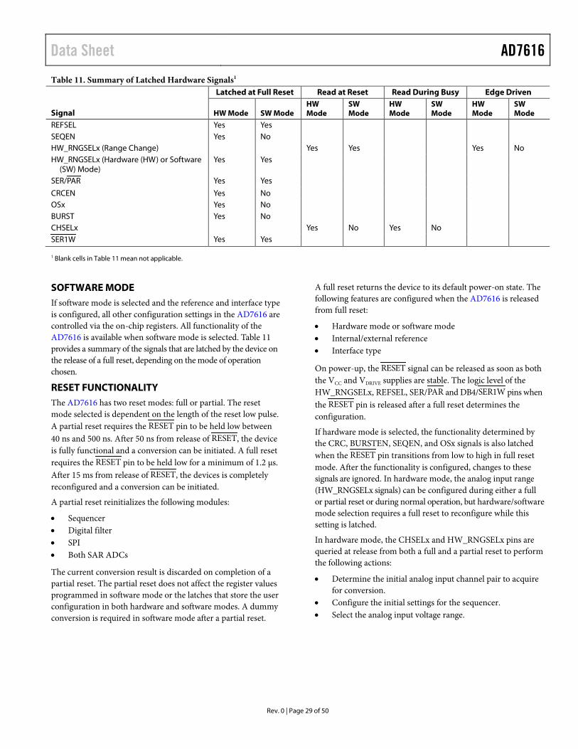
Data Sheet AD7616
Rev. 0 | Page 29 of 50
Table 11. Summary of Latched Hardware Signals1
Signal
Latched at Full Reset Read at Reset Read During Busy Edge Driven
HW Mode SW Mode HW Mode
SW Mode
HW Mode
SW Mode
HW Mode
SW Mode
REFSEL Yes Yes SEQEN Yes No HW_RNGSELx (Range Change) Yes Yes Yes No HW_RNGSELx (Hardware (HW) or Software
(SW) Mode) Yes Yes
SER/PAR Yes Yes
CRCEN Yes No OSx Yes No BURST Yes No CHSELx Yes No Yes No SER1W Yes Yes 1 Blank cells in Table 11 mean not applicable.
SOFTWARE MODE If software mode is selected and the reference and interface type is configured, all other configuration settings in the AD7616 are controlled via the on-chip registers. All functionality of the AD7616 is available when software mode is selected. Table 11 provides a summary of the signals that are latched by the device on the release of a full reset, depending on the mode of operation chosen.
RESET FUNCTIONALITY The AD7616 has two reset modes: full or partial. The reset mode selected is dependent on the length of the reset low pulse. A partial reset requires the RESET pin to be held low between 40 ns and 500 ns. After 50 ns from release of RESET, the device is fully functional and a conversion can be initiated. A full reset requires the RESET pin to be held low for a minimum of 1.2 µs. After 15 ms from release of RESET, the devices is completely reconfigured and a conversion can be initiated.
A partial reset reinitializes the following modules:
• Sequencer • Digital filter • SPI • Both SAR ADCs
The current conversion result is discarded on completion of a partial reset. The partial reset does not affect the register values programmed in software mode or the latches that store the user configuration in both hardware and software modes. A dummy conversion is required in software mode after a partial reset.
A full reset returns the device to its default power-on state. The following features are configured when the AD7616 is released from full reset:
• Hardware mode or software mode • Internal/external reference • Interface type
On power-up, the RESET signal can be released as soon as both the VCC and VDRIVE supplies are stable. The logic level of the HW_RNGSELx, REFSEL, SER/PAR and DB4/SER1W pins when the RESET pin is released after a full reset determines the configuration.
If hardware mode is selected, the functionality determined by the CRC, BURSTEN, SEQEN, and OSx signals is also latched when the RESET pin transitions from low to high in full reset mode. After the functionality is configured, changes to these signals are ignored. In hardware mode, the analog input range (HW_RNGSELx signals) can be configured during either a full or partial reset or during normal operation, but hardware/software mode selection requires a full reset to reconfigure while this setting is latched.
In hardware mode, the CHSELx and HW_RNGSELx pins are queried at release from both a full and a partial reset to perform the following actions:
• Determine the initial analog input channel pair to acquire for conversion.
• Configure the initial settings for the sequencer. • Select the analog input voltage range.

AD7616 Data Sheet
Rev. 0 | Page 30 of 50
The CHSELx and HW_RNGSELx signals are not latched. The channel pair selected for conversion, or the hardware sequencer, can be reconfigured during normal operation by setting and maintaining the CHSELx signal level before the CONVST rising edge, and ensuring the signal level remains constant until after BUSY transitions low again. See the Channel Selection section for further details.
In software mode, all additional functionality is configured by controlling the on-chip registers.
PIN FUNCTION OVERVIEW There are several dual function pins on the AD7616. Their functionality is dependent on the mode of operation selected by the HW_RNGSELx pins. Table 12 outlines the pin functionality in the different modes of operation and interface modes.
Figure 50. AD7616 Configuration at Reset
Table 12. Pin Functionality Overview
Pins
Operation Mode Software, HW_RNGSELx = 00 Hardware, HW_RNGSELx ≠ 00
Serial, SER/PAR = 1 Parallel, SER/PAR = 0 Serial, SER/PAR = 1 Parallel, SER/PAR = 0
CHSELx No function, connect to DGND
No function, connect to DGND
CHSELx CHSELx
SCLK/RD SCLK RD SCLK RD
WR/BURST Connect to DGND WR BURST BURST
DB15/OS0 to DB13/OS2
Connect to DGND DB15 to DB13 OSx DB15 to DB13
DB12/SDOA SDOA DB12 SDOA DB12 DB11/SDOB SDOB, leave floating for
serial 1-wire mode DB11 SDOB DB11
DB10/SDI SDI DB10 Connect to DGND DB10 DB9 to DB6, DB3
to DB0 Connect to DGND DB9 to DB6, DB3 to
DB0 Connect to DGND DB9 to DB6, DB3 to DB0
DB5/CRCEN Connect to DGND DB5 CRCEN DB5 DB4/SER1W SER1W DB4 SER1W DB4
HW_RNGSELx HW_RNGSELx, connect to DGND
HW_RNGSELx, connect to DGND
HW_RNGSELx, configure analog input range
HW_RNGSELx, configure analog input range
SEQEN No function, connect to DGND
No function, connect to DGND
SEQEN SEQEN
REFSEL REFSEL REFSEL REFSEL REFSEL
VCCVDRIVE
RESET
CONVST
BUSY
MODE RANGE SETTING IN HW MODE
CHx y z
ACQx CONVx ACQy CONVy
tRESET_WAIT
tDEVICE_SETUP
tRESET_SETUP
tRESET_HOLD
ALL MODES
HARDWAREMODE ONLY
1359
1-01
2
REFSELSER/PAR, SER1W
HW_RNGSEL0,HW_RNGSEL1
CRCEN, BURSTSEQEN, OS0 TO OS2
CHSEL0 TO CHSEL2
ACTION

Data Sheet AD7616
Rev. 0 | Page 31 of 50
DIGITAL INTERFACE CHANNEL SELECTION Hardware Mode
The logic level of the CHSELx signals determine the channel pair for conversion; see Table 13 for signal decoding information. The CHSELx signals at the time that either full or partial reset is released determine the initial channel pair to sample. After a reset, the logic levels of the CHSELx signals are examined during the BUSY high period to set the channel pair for the next conversion. The CHSELx signal level must be set before CONVST goes from low to high and be maintained until BUSY goes from high to low to indicate a conversion is complete. See Figure 51 for further details.
Software Mode
In software mode, the channels for conversion are selected by control of the channel register. On power-up or after a reset, the default channels selected for conversion are Channel V0A and Channel V0B.
Table 13. CHSELx Pin Decoding Channel Selection Input Pin Analog Input Channels for
Conversion CHSEL0 CHSEL1 CHSEL2 0 0 0 V0A, V0B 0 0 1 V1A, V1B 0 1 0 V2A, V2B 0 1 1 V3A, V3B 1 0 0 V4A, V4B 1 0 1 V5A, V5B 1 1 0 V6A, V6B 1 1 1 V7A, V7B
Figure 51. Hardware Mode Channel Conversion Setting
Figure 52. Software Serial Mode Channel Conversion Setting
Figure 53. Software Parallel Mode Channel Conversion Setting
1359
1-01
3
RESET
CONVST
BUSY
CHx
A/Bx A/By A/Bz
CHy CHz CH...CHSEL2
TOCHSEL0
DATA BUS
CONFIGURE POINT CONFIGURE POINT CONFIGURE POINTINITIAL SETUP
RESET
CONVST
BUSY
CS
WRITE CHx WRITE CHy WRITE CHz WRITE CH...SDI
A/B0 A/Bx A/BySDOA,SDOB
CHx CONVERSION START
DO NOT CARE
1359
1-01
4
RESET
CONVST
BUSY
CS
WR
RD
CHx A0 B0 CHy Ax Bx CHz Ay By CH...DB0 TO
DB15
CHx CONVERSION START 1359
1-15
3
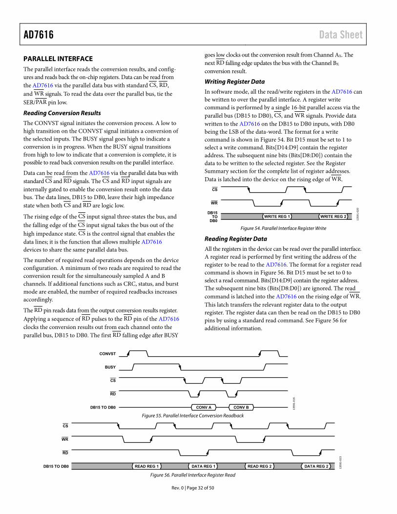
AD7616 Data Sheet
Rev. 0 | Page 32 of 50
PARALLEL INTERFACE The parallel interface reads the conversion results, and config-ures and reads back the on-chip registers. Data can be read from the AD7616 via the parallel data bus with standard CS, RD, and WR signals. To read the data over the parallel bus, tie the SER/PAR pin low.
Reading Conversion Results
The CONVST signal initiates the conversion process. A low to high transition on the CONVST signal initiates a conversion of the selected inputs. The BUSY signal goes high to indicate a conversion is in progress. When the BUSY signal transitions from high to low to indicate that a conversion is complete, it is possible to read back conversion results on the parallel interface.
Data can be read from the AD7616 via the parallel data bus with standard CS and RD signals. The CS and RD input signals are internally gated to enable the conversion result onto the data bus. The data lines, DB15 to DB0, leave their high impedance state when both CS and RD are logic low.
The rising edge of the CS input signal three-states the bus, and the falling edge of the CS input signal takes the bus out of the high impedance state. CS is the control signal that enables the data lines; it is the function that allows multiple AD7616 devices to share the same parallel data bus.
The number of required read operations depends on the device configuration. A minimum of two reads are required to read the conversion result for the simultaneously sampled A and B channels. If additional functions such as CRC, status, and burst mode are enabled, the number of required readbacks increases accordingly.
The RD pin reads data from the output conversion results register. Applying a sequence of RD pulses to the RD pin of the AD7616 clocks the conversion results out from each channel onto the parallel bus, DB15 to DB0. The first RD falling edge after BUSY
goes low clocks out the conversion result from Channel AX. The next RD falling edge updates the bus with the Channel BX conversion result.
Writing Register Data
In software mode, all the read/write registers in the AD7616 can be written to over the parallel interface. A register write command is performed by a single 16-bit parallel access via the parallel bus (DB15 to DB0), CS, and WR signals. Provide data written to the AD7616 on the DB15 to DB0 inputs, with DB0 being the LSB of the data-word. The format for a write command is shown in Figure 54. Bit D15 must be set to 1 to select a write command. Bits[D14:D9] contain the register address. The subsequent nine bits (Bits[D8:D0]) contain the data to be written to the selected register. See the Register Summary section for the complete list of register addresses. Data is latched into the device on the rising edge of WR.
Figure 54. Parallel Interface Register Write
Reading Register Data
All the registers in the device can be read over the parallel interface. A register read is performed by first writing the address of the register to be read to the AD7616. The format for a register read command is shown in Figure 56. Bit D15 must be set to 0 to select a read command. Bits[D14:D9] contain the register address. The subsequent nine bits (Bits[D8:D0]) are ignored. The read command is latched into the AD7616 on the rising edge of WR. This latch transfers the relevant register data to the output register. The register data can then be read on the DB15 to DB0 pins by using a standard read command. See Figure 56 for additional information.
Figure 55. Parallel Interface Conversion Readback
Figure 56. Parallel Interface Register Read
CS
WR
WRITE REG 1 WRITE REG 2
1359
1-02
0
DB15TO
DB0
CONVST
BUSY
CS
RD
CONV A CONV BDB15 TO DB0 1359
1-01
6
CS
WR
RD
READ REG 1 DATA REG 1 READ REG 2 DATA REG 2 1359
1-02
3
DB15 TO DB0

Data Sheet AD7616
Rev. 0 | Page 33 of 50
SERIAL INTERFACE
To interface to the AD7616 over the SPI, the SER/PAR pin must be tied high. The CS and SCLK signals transfer data from the AD7616. The AD7616 has two serial data output pins, SDOA and SDOB. Data is read back from the AD7616 using serial 1-wire or serial 2-wire mode.
In serial 2-wire mode for the AD7616, conversion results from Channel V0A to Channel V7A appear on SDOA, and conversion results from Channel V0B to Channel V7B appear on SDOB. In serial 1-wire mode, conversion results from Channel V0B to Channel V7B are interlaced with conversion results from Channel V0A to Channel V7A. To achieve the maximum throughput, it is required to use 2-wire mode.
To read back data over both SDOA and SDOB, the SER1W pin must be tied high. If data is to be read back over SDOA only, the SER1W pin must be tied low. Serial 1-wire or 2-wire mode is configured when the AD7616 is released from full reset.
Reading Conversion Results
The CONVST signal initiates the conversion process. A low to high transition on the CONVST signal initiates a conversion of the selected inputs. The BUSY signal goes high to indicate a conversion is in progress. When the BUSY signal transitions from high to low to indicate that a conversion is complete, it is possible to read back conversion results on the serial interface.
The CS falling edge takes the data output lines, SDOA and SDOB, out of three-state and clocks out the MSB of the conversion result. The rising edge of SCLK clocks all subsequent data bits
onto the serial data outputs, SDOA and SDOB. Figure 57 shows a read of two simultaneous conversion results using two SDOx lines on the AD7616. If the status register is appended to the conversion results or operating in sequencer burst mode where multiples of 16 SCLK transfers access data from the AD7616, hold CS low to frame the entire data. Data can also be clocked out using just one SDOx line, in which case SDOA must be used to access all conversion data. For the AD7616 to access both Channel VxA and Channel VxB conversion results on one SDOx line, a total of 32 SCLK cycles is required. Frame these 32 SCLK cycles using one CS signal, or individually frame each group of 16 SCLK cycles using the CS signal. The disadvantage of using just one SDOx line is that the throughput rate is reduced.
Leave the unused SDOB line unconnected in serial 1-wire mode. If using SDOA as a single serial data output line, the channel results are output in the following order: VxA and VxB. Figure 58 shows a 1-wire, serial readback operation.
The speed at which the data can be read back in serial interface mode is dependent on SPI frequency, VDRIVE supply, and the capacitance of the load on the SDO line, CLOAD. Table 14 shows a summary of the maximum speed achievable for various conditions.
Table 14. SPI Frequency vs. Load Capacitance and VDRIVE VDRIVE (V) CLOAD (pF) SPI Frequency (MHz) 2.3 to 3 20 40 3 to 3.6 30 50
Figure 57. Serial Interface, 2-Wire Mode
Figure 58. Serial Interface, 1-Wire Mode
CONVST
BUSY
CS
1 2 3 14 15 16SCLK
SDOA
DB15 DB14 DB13 DB2 DB1 DB0
DB15 DB14 DB13 DB2 DB1 DB0
SDOB
CHANNEL VAx RESULT
CHANNEL VBx RESULT 1359
1-01
7
CONVST
BUSY
CS
1 2 15 16 17 18 31 32SCLK
DB15 DB14 DB1 DB0 DB15 DB14 DB1 DB0SDOA
CHANNEL VAx RESULT CHANNEL VBx RESULT 1359
1-01
8
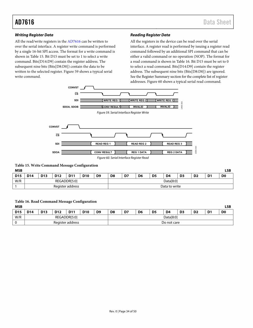
AD7616 Data Sheet
Rev. 0 | Page 34 of 50
Writing Register Data
All the read/write registers in the AD7616 can be written to over the serial interface. A register write command is performed by a single 16-bit SPI access. The format for a write command is shown in Table 15. Bit D15 must be set to 1 to select a write command. Bits[D14:D9] contain the register address. The subsequent nine bits (Bits[D8:D0]) contain the data to be written to the selected register. Figure 59 shows a typical serial write command.
Reading Register Data
All the registers in the device can be read over the serial interface. A register read is performed by issuing a register read command followed by an additional SPI command that can be either a valid command or no operation (NOP). The format for a read command is shown in Table 16. Bit D15 must be set to 0 to select a read command. Bits[D14:D9] contain the register address. The subsequent nine bits (Bits[D8:D0]) are ignored. See the Register Summary section for the complete list of register addresses. Figure 60 shows a typical serial read command.
Figure 59. Serial Interface Register Write
Figure 60. Serial Interface Register Read
Table 15. Write Command Message Configuration MSB LSB D15 D14 D13 D12 D11 D10 D9 D8 D7 D6 D5 D4 D3 D2 D1 D0 W/R REGADDR[5:0] Data[8:0] 1 Register address Data to write
Table 16. Read Command Message Configuration MSB LSB D15 D14 D13 D12 D11 D10 D9 D8 D7 D6 D5 D4 D3 D2 D1 D0 W/R REGADDR[5:0] Data[8:0] 0 Register address Do not care
CONVST
CS
WRITE REG 1 WRITE REG 2 WRITE REG 3SDI
CONV RESULT INVALID INVALIDSDOA, SDOB
1359
1-02
1
CONVST
CS
READ REG 1 READ REG 2 READ REG 3SDI
CONV RESULT REG 1 DATA REG 2 DATASDOA 1359
1-02
4

Data Sheet AD7616
Rev. 0 | Page 35 of 50
SEQUENCER The AD7616 features a highly configurable on-chip sequencer. The functionality and configuration of the sequencer is dependent on the mode of operation of the AD7616.
In hardware mode, the sequencer is sequential only. The sequencer always starts converting at Channel V0A and Channel V0B and converts each subsequent channel up to the configured end channel.
In software mode, the sequencer has additional functionality and configurability. The sequencer stack has 32 uniquely configurable sequence steps, allowing any channel order to be programmed. Additionally, any Channel VxA input can be paired with any Channel VxB input or diagnostic channel.
The sequencer can be operated with or without the burst function enabled. With the burst function enabled, only one CONVST pulse is required to convert every channel in a sequence. With burst mode disabled, one CONVST pulse is required for every conversion step in the sequence. See the Burst Sequencer section for additional details on operating in burst mode.
HARDWARE MODE SEQUENCER In hardware mode, the sequencer is controlled by the SEQEN pin and the CHSELx pins. The sequencer is enabled or disabled when the AD7616 is released from full reset. The logic level of the SEQEN pin when the RESET pin is released determines whether the sequencer is enabled or disabled (see Table 17 for settings). After the RESET pin is released, the function is fixed and a full reset via the RESET pin is required to exit the function and set up an alternative configuration.
Table 17. Hardware Mode Sequencer Configuration SEQEN Interface Mode 0 Sequencer disabled 1 Sequencer enabled
When the sequencer is enabled, the logic levels of the CHSELx pins determine the channels selected for conversion in the sequence. The CHSELx pins at the time RESET is released determine the initial settings for the channels to convert in the sequence. To reconfigure the channels selected for conversion thereafter, set the CHSELx pins to the required setting for the duration of the final BUSY pulse before the current conversion sequence is complete. See Figure 61 for further details.
Table 18. CHSELx Pin Decoding Sequencer Channel Selection Input Pin Analog Input Channels for
Sequential Conversion CHSEL0 CHSEL1 CHSEL2 0 0 0 V0x only 0 0 1 V0x to V1x 0 1 0 V0x to V2x 0 1 1 V0x to V3x 1 0 0 V0x to V4x 1 0 1 V0x to V5x 1 1 0 V0x to V6x 1 1 1 V0x to V7x
SOFTWARE MODE SEQUENCER In software mode, the AD7616 contains a 32-layer fully configurable sequencer stack. Control of the sequencer is achieved by programming the configuration register and sequencer stack registers via the parallel or serial interface.
Each stack step can be individually programmed to pair any input from Channel VxA to any input from Channel VxB, or any diagnostic channel can be selected for conversion. The sequencer depth can be set to any length from 1 to 32 layers. The sequencer depth is controlled via the SSRENx bit. Set the SSRENx bit in the sequencer stack register corresponding to the last step required. The channels to convert are selected by programming the ASELx and BSELx bits in each sequence stack register for the depth required.
The sequencer is activated by setting the SEQEN bit in the configuration register to 1.
Figure 61. Hardware Mode Sequencer Configuration
RESET
SEQEN
CONVST
BUSY
CHx CHy CHzCHSEL2 TO CHSEL0
A/B0 A/Bx A/B0 A/By A/B0DATA
INITIAL SETUP CONFIGURE POINT CONFIGURE POINT
A/Bx-1 A/By-1
1359
1-02
5

AD7616 Data Sheet
Rev. 0 | Page 36 of 50
To configure and enable the sequencer, it is recommended to complete the following procedure (see Figure 62):
1. Configure the analog input range for the required analog input channels.
2. Program the sequencer stack registers to select the channels for the sequence.
3. Set the SSRENx bit in the last required sequence step. 4. Set the SEQEN bit in the configuration register. 5. Provide a dummy CONVST pulse. 6. Cycle through CONVST pulses and conversion reads to step
through each element of the sequencer stack.
The sequence automatically restarts from the first element in the sequencer stack with the next CONVST pulse.
Following a partial reset, the sequencer pointer is repositioned to the first layer of the stack, but the register programmed values remain unchanged.
BURST SEQUENCER Burst mode avoids generating a CONVST pulse for each step in a sequence of conversions. One CONVST pulse converts every step in the sequence.
The burst sequencer is an additional feature that works in conjunction with the sequencer. If the burst function is enabled, one CONVST pulse initiates a conversion of all the channels configured in the sequencer. The burst function avoids generating a CONVST pulse for each step in a sequence of conversions, as is the case when the burst function is disabled.
Configuration of the burst function varies depending on the mode of operation: hardware or software mode. See the Hardware Mode Burst section and the Software Mode Burst section for specific details on configuring the burst function in the each mode.
When configured, the burst sequence is initiated at the rising edge of CONVST. The BUSY pin goes high to indicate that a conversion is in progress. The BUSY pin remain highs until all conversions in the sequence are complete. The conversion results are available for readback after the BUSY pin goes low.
The number of data reads required to read all the data in the burst sequence is dependent on the length of the sequence configured.
The conversion results are presented on the data bus (parallel or serial) in the same order as the programmed sequence.
The throughput rate of the AD7616 is limited in burst mode and dependent on the length of the sequence. Each channel pair requires an acquisition, conversion, and readback time. The time taken to complete a sequence with number of channel pairs, N, is estimated by
tBURST = (tCONV + 25 ns) + (N – 1)(tACQ + tCONV) + N(tRB)
where: tCONV is the typical conversion time. tACQ is typical acquisition time. tRB is the time required to read back the conversion results in either serial 1-wire, serial 2-wire, or parallel mode.
Hardware Mode Burst
Burst mode is enabled in hardware mode by setting the BURST pin to 1. The SEQEN pin must also be set to 1 to enable the sequencer.
In hardware mode, the burst sequencer is controlled by the BURST, SEQEN, and CHSELx pins. The burst sequencer is enabled or disabled when the AD7616 is released from full reset. The logic level of the SEQEN pin and the BURST pin when the RESET pin is released determines whether the burst sequencer is enabled or disabled. After the RESET pin is released, the function is fixed and a full reset via the RESET pin is required to exit the function and set up an alternative configuration.
When the burst sequencer is enabled, the logic levels of the CHSELx pins determine the channels selected for conversion in the burst sequence. The CHSELx pins at the time RESET is released determines the initial settings for the channels to convert in the burst sequence. To reconfigure the channels selected for conver-sion after a reset, set the CHSELx pins to the required setting for the duration of the next BUSY pulse (see Figure 63 for further details).
Software Mode Burst
In software mode, the burst function is enabled by setting the BURST bit in the configuration register to 1. This action must be performed when setting the SEQEN bit in the configuration register as outlined in the steps described in the Software Mode Sequencer section to configure the sequencer (see Figure 64 for additional information).
Figure 62. Software Mode Sequencer Configuration
RESET
CONVST
BUSY
REGISTERSETUP
A/B0 S0 S1 Sn – 1 Sn S0DATA
INITIAL SETUP SEQUENCE START
DUMMY CONVERSION
SEQUENCE START
1359
1-02
6

Data Sheet AD7616
Rev. 0 | Page 37 of 50
Figure 63. BURST Sequencer, Hardware Mode
Figure 64. BURST Sequencer, Software Mode
RESET
SEQEN
BURST
CONVST
BUSY
CHx CHy CHz CHz CHz
CHSEL2TO
CHSEL0
A/B0 A/Bx–1 A/Bx A/B0 A/By–1 A/By A/B0 A/Bz–1 A/BzDATA
CONFIGURE POINT CONFIGURE POINT CONFIGURE POINTINITIAL SETUP 1359
1-02
7
RESET
CONVST
BUSY
REGISTERSETUP
A/B0 S0 S1 Sn–1 Sn S0 S1 Sn–1 SnDATA
DUMMY CONVERSION 1359
1-02
8

AD7616 Data Sheet
Rev. 0 | Page 38 of 50
DIAGNOSTICS DIAGNOSTIC CHANNELS In addition to the 16 analog inputs, VxA and VxB, the AD7616 can also convert the following diagnostic channels: VCC and the analog ALDO voltage. The diagnostic channels are selected for conversion by programming the channel register (see the Channel Register section) to the corresponding channel identifier. Diagnos-tic channels can also be added to the sequencer stack in software mode, but only provide an accurate reading at throughput rates <250 kSPS. See Figure 65 for a plot of the deviation from expected value vs. sampling frequency that can be expected when using the diagnostic channels.
The expected output for each channel is governed by the following transfer functions:
( )( )REF
REFCCCC V
VVCodeV
×××
=5
768,32–4
( ) ( )( )REF
REFALDO
VVV
CodeLDO×
×××=
10768,327–10
Figure 65. Deviation from Expected Value vs. Sampling Frequency
Figure 66. VCC Diagnostic Transfer Function
Figure 67. ALDO Diagnostic Transfer Function
INTERFACE SELF TEST It is possible to test the integrity of the digital interface by selecting the communication self test channel in the channel register (see the Channel Register section).
Selecting the communication self test for conversion forces the conversion result register to a known fixed output. When conversion code is read, Code 0xAAAA is output as the conversion code of ADC A, and Code 0x5555 is output as the conversion code of ADC B.
CRC The AD7616 has a cyclic redundancy check (CRC) checksum mode to improve interface robustness by detecting errors in data. The CRC feature is available in both software (serial and parallel) mode and hardware (serial only) mode. The CRC feature is not available in hardware parallel mode. The CRC result is contained within the status register. Enabling the CRC feature enables the status register and vice versa.
In hardware mode, the CRCEN pin controls the CRC feature. The CRC feature is enabled or disabled when the AD7616 is released from full reset. The logic level of the CRCEN pin when the RESET pin is released determines whether the CRC feature is enabled or disabled. Set the CRCEN pin to 1 to enable the CRC feature. After the RESET pin is released, the function is fixed and a full reset via the RESET pin is required to exit the function and set up an alternative configuration. See the Reset Functionality section for additional information. After being enabled, the CRC result is appended to the conversion result and consists of a 16-bit word, where the first eight bits contain the channel ID of the last channel pair converted and the last eight bits are the CRC result. The result is accessed via an extra read command, as shown in Figure 68.
In software mode, the CRC function is enabled by setting either the CRCEN bit or the STATUSEN bit in the configuration register to 1 (see the section).
750
–750
–500
–250
0
250
500
0 600500400300200100SAMPLING FREQUENCY (kSPS)
DEV
IATI
ON
FR
OM
EXP
ECTE
D V
ALU
E (C
odes
)
1359
1-03
5
ALDO ERROR
VCC ERROR
29000
22000
23000
24500
26000
28000
25000
27000
4.50 4.75 5.00 5.505.25
EXPE
CTE
D O
UTP
UT
(Cod
es)
VCC (V)
1359
1-02
9
1359
1-03
0–9000
–8800
–8600
–8400
–8200
–8000
–7800
–7600
–7400
–7200
1.75 1.80 1.85 1.90 1.95
EXPE
CTE
D O
UTP
UT
(Cod
es)
ALDO (V)

Data Sheet AD7616
Rev. 0 | Page 39 of 50
If the CRC function is enabled, a CRC is calculated on the conversion results for Channel VxA and Channel VxB. The CRC is calculated and transferred on the serial or parallel interface after the conversion results are transmitted, depending on the configuration of the device. The Hamming distance varies relative to the number of bits in the conversion result. For conversions with ≤119 bits, the Hamming distance is 4. For >119 bits, the Hamming distance is 1, that is, 1-bit errors are always detected.
The following is a pseudocode description of how the CRC is implemented in the AD7616:
crc = 8’b0;
i = 0;
x = number of conversion channel pairs;
for (i=0, i<x, i++) begin
crc1 = crc_out(An,Crc);
crc = crc_out(Bn,Crc1);
i = i +1;
end
where the function crc_out(data, crc) is
crc_out[0] = data[14] ^ data[12] ^ data[8] ^ data[7] ^ data[6] ^ data[0] ^ crc[0] ^ crc[4] ^ crc[6];
crc_out[1] = data[15] ^ data[14] ^ data[13] ^ data[12] ^ data[9] ^ data[6] ^ data[1] ^ data[0] ^ crc[1] ^ crc[4] ^ crc[5] ^ crc[6] ^ crc[7];
crc_out[2] = data[15] ^ data[13] ^ data[12] ^ data[10] ^ data[8] ^ data[6] ^ data[2] ^ data[1] ^ data[0] ^ crc[0] ^ crc[2] ^ crc[4] ^ crc[5] ^ crc[7];
crc_out[3] = data[14] ^ data[13] ^ data[11] ^ data[9] ^ data[7] ^ data[3] ^ data[2] ^ data[1] ^ crc[1] ^ crc[3] ^ crc[5] ^ crc[6];
crc_out[4] = data[15] ^ data[14] ^ data[12] ^ data[10] ^ data[8] ^ data[4] ^ data[3] ^ data[2] ^ crc[0] ^ crc[2] ^ crc[4] ^ crc[6] ^ crc[7];
crc_out[5] = data[15] ^ data[13] ^ data[11] ^ data[9] ^ data[5] ^ data[4] ^ data[3] ^ crc[1] ^ crc[3] ^ crc[5] ^ crc[7];
crc_out[6] = data[14] ^ data[12] ^ data[10] ^ data[6] ^ data[5] ^ data[4] ^ crc[2] ^ crc[4] ^ crc[6];
crc_out[7] = data[15] ^ data[13] ^ data[11] ^ data[7] ^ data[6] ^ data[5] ^ crc[3] ^ crc[5] ^ crc[7];
The initial CRC word used by the AD7616 is an 8-bit word equal to zero. The XOR operation described in the preceding code is executed to calculate each bit of the CRC word for the conversion result, AN. This CRC word (crc1) is then used as the starting point for calculating the CRC word (crc) for the conversion result, BN. The process repeats cyclically for each channel pair converted.
Depending on the mode of operation of the AD7616, the status register value is appended to the conversion data and read out via an extra read command over the serial or parallel interface. The user can then repeat the XOR calculation described in the preceding code for the received conversion results to check whether both CRC words match. See Figure 68 or a description of how the CRC word is appended to the data for each mode of operation.
Figure 68. CRC Readback for All Modes
CONVST
BUSY
Ax Bx CRCAB(x)DATA
Ax Bx Az Bz CRCAB(x:z)DATA
Ax CRCAB(x)SDOA
Bx CRCAB(x)SDOB
Ax Az CRCAB(x:z)SDOA
Bx Bz CRCAB(x:z)SDOB
PARALLEL/SERIAL (1-WIRE),SEQUENCER/MANUAL MODE
PARALLEL/SERIAL (1-WIRE),BURST
SERIAL (2-WIRE),SEQUENCER/MANUAL MODE
SERIAL (2-WIRE),BURST
1359
1-03
2
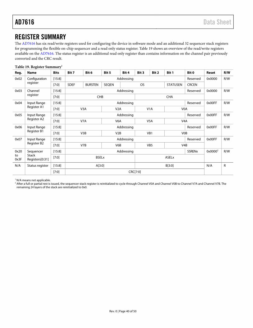
AD7616 Data Sheet
Rev. 0 | Page 40 of 50
REGISTER SUMMARY The AD7616 has six read/write registers used for configuring the device in software mode and an additional 32 sequencer stack registers for programming the flexible on-chip sequencer and a read only status register. Table 19 shows an overview of the read/write registers available on the AD7616. The status register is an additional read only register than contains information on the channel pair previously converted and the CRC result.
Table 19. Register Summary1 Reg. Name Bits Bit 7 Bit 6 Bit 5 Bit 4 Bit 3 Bit 2 Bit 1 Bit 0 Reset R/W
0x02 Configuration register
[15:8] Addressing Reserved 0x0000 R/W
[7:0] SDEF BURSTEN SEQEN OS STATUSEN CRCEN
0x03 Channel register
[15:8] Addressing Reserved 0x0000 R/W
[7:0] CHB CHA
0x04 Input Range Register A1
[15:8] Addressing Reserved 0x00FF R/W
[7:0] V3A V2A V1A V0A
0x05 Input Range Register A2
[15:8] Addressing Reserved 0x00FF R/W
[7:0] V7A V6A V5A V4A
0x06 Input Range Register B1
[15:8] Addressing Reserved 0x00FF R/W
[7:0] V3B V2B VB1 V0B
0x07 Input Range Register B2
[15:8] Addressing Reserved 0x00FF R/W
[7:0] V7B V6B VB5 V4B
0x20 to 0x3F
Sequencer Stack Registers[0:31]
[15:8] Addressing SSRENx 0x00002 R/W
[7:0] BSELx ASELx
N/A Status register [15:8] A[3:0] B[3:0] N/A R
[7:0] CRC[7:0] 1 N/A means not applicable. 2 After a full or partial rest is issued, the sequencer stack register is reinitialized to cycle through Channel V0A and Channel V0B to Channel V7A and Channel V7B. The
remaining 24 layers of the stack are reinitialized to 0x0.

Data Sheet AD7616
Rev. 0 | Page 41 of 50
ADDRESSING REGISTERS The seven MSBs written to the device are decoded to determine which register is addressed. The seven MSBs consist of the register address (REGADDR), Bits[5:0], and the read/write bit. The register address bits determine which on-chip register is selected. The read/write bit determines if the remaining nine bits of data on the DB10/SDI lines are loaded into the addressed register. If the read/write bit is 1, the bits load into the register addressed by the register select bits. If the read/write bit is 0, the command is seen as a read request. The addressed register data is available to be read during the next read operation.
MSB LSB D15 D14 D13 D12 D11 D10 D9 D8 to D0 W/R REGADDR[5] REGADDR[4] REGADDR[3] REGADDR[2] REGADDR[1] REGADDR[0] DATA[8:0]
Table 20. Bit s Mnemonic Description D15 W/R If a 1 is written to this bit, Bits[D8:D0] of this register are written to the register specified by REGADDR[5:0].
Alternatively, if a 0 is written, the next operation is a read from the designated register.
D14 REGADDR[5] If a 1 is written to this bit, the contents of REGADDR[4:0] specifies the 32 sequencer stack registers. Alternatively, if a 0 is written to this bit, a register is selected as defined by REGADDR[4:0].
[D13:D9] REGADDR[4:0] When W/R =1, the contents of REGADDR[4:0] determine register for selection as follows:
00001: reserved. 00010: selects the configuration register. 00011: selects the channel register. 00100: selects Input Range Register A1. 00101: selects Input Range Register A2. 00110: selects Input Range Register B1. 00111: selects Input Range Register B2. 01000: selects the status register When W/R = 0, and REGADDR[4:0] contains 00000, the conversion codes are read.
[D8:D0] DATA[8:0] These bits are written into the corresponding register specified by Bits REGADDR[5:0]. See the following sections for detailed descriptions of each register.

AD7616 Data Sheet
Rev. 0 | Page 42 of 50
CONFIGURATION REGISTER The configuration register is used in software mode to configure many of the main functions of the ADC, including the sequencer, burst mode, oversampling, and CRC options.
Address: 0x02, Reset: 0x0000, Name: Configuration Register
Table 21. Bit Descriptions for the Configuration Register Bits Bit Name Settings Description Reset1 Access [15:9] Addressing 0 Bits[15:9] define the address of the relevant register. See the Addressing Registers
section for further details. 0x0 RW
8 RESERVED Reserved. 0x0 R/W 7 SDEF Self detector error flag. N/A R 0 Test passed. The AD7616 has configured itself successfully after power-up. 1 Test failed. An issue was detected during device configuration. A reset is required. 6 BURSTEN Burst mode enable. 0x0 RW 0 Burst mode is disabled. Each channel pair to be converted requires a CNVST pulse. 1 A single CNVST pulse converts every channel pair programmed in the 32-layer
sequencer stack registers up to and including the layer defined by the SSRENx bit. See the Software Mode Sequencer section and the Software Mode Burst section for further details.
5 SEQEN Channel sequencer enable. 0x0 RW 0 The channel sequencer is disabled. 1 The channel sequencer is enabled. [4:2] OS Oversampling (OS) ratio, samples per channel. 0x0 RW 000 Oversampling disabled. 001 Oversampling enabled, OSR = 2. 010 Oversampling enabled, OSR = 4. 011 Oversampling enabled, OSR = 8. 100 Oversampling enabled, OSR = 16. 101 Oversampling enabled, OSR = 32. 110 Oversampling enabled, OSR = 64. 111 Oversampling enabled, OSR = 128. 1 STATUSEN Status register output enable. 0x0 RW 0 The status register is not read out when reading the conversion result. 1 The status register is read out at the end of all the conversion words (including the
self test channel if enabled in sequencer mode) if all the selected channels are read out. The CRC result is included in the last eight bits.
0 CRCEN CRC enable. The STATUSEN and CRCEN bits have identical functionality. 0x0 RW 1 N/A means not applicable.
CRC Enable
Status Register Output EnableSelf-Detector Error flag
OS ratio samples per channel
111: OS128.110: OS64.101: OS32.100: OS16.011: OS8.010: OS4.001: OS2.000: OS1.Burst Mode enable
Channel Sequencer Enable
0
01
02
03
04
05
06
07
08
09
010
011
012
013
014
015
0
[15:9] Addressing (R/W) [0] CRCEN (R/W)
[8] RESERVED[1] STATUSEN (R/W)[7] SDEF (R)
[4:2] OS (R/W)[6] BURSTEN (R/W)
[5] SEQEN (R/W)

Data Sheet AD7616
Rev. 0 | Page 43 of 50
CHANNEL REGISTER Address: 0x03, Reset: 0x0000, Name: Channel Register
In software manual mode, the channel register selects the input channel or self test channel for the next conversion.
Table 22. Bit Descriptions for the Channel Register Bits Bit Name Settings Description Reset Access
[15:9] Addressing Bits[15:9] define the address of the relevant register. See the Addressing Registers section for further details.
0x0 R/W
8 RESERVED Reserved. 0x0 R/W
[7:4] CHB Channel selection bits for ADC B channels.
0000 V0A/V0B.
0001 V1A/V1B.
0010 V2A/V2B.
0011 V3A/V3B.
0100 V4A/V4B.
0101 V5A/V5B.
0110 V6A/V6B.
0111 V7A/V7B.
1000 VCC.
1001 ALDO.
1010 Reserved.
1011 Set the dedicated bits for digital interface communication self test function. When conversion codes are read, Code 0xAAAA is read out as the conversion code of Channel A, and Code 0x5555 is output as the conversion code of Channel B.
1100 Reserved.
[3:0] CHA Channel selection bits for ADC A Channels. Settings are the same as for ADC B. 0x0 R/W
Channel Selection bits for ADC AChannels
1100: Reserved.1011: 0XAAAA.1010: Reserved.
...10: V2A.
1: V1A.0: V0A.
Channel Selection bits for ADC BChannels
1100: Reserved.1011: 0x5555.1010: Reserved.
...10: V2B.
1: V1B.0: V0B.
0
01
02
03
04
05
06
07
08
09
010
011
012
013
014
015
0
[15:9] Addressing (R/W) [3:0] CHA (R/W)
[8] RESERVED
[7:4] CHB (R/W)

AD7616 Data Sheet
Rev. 0 | Page 44 of 50
INPUT RANGE REGISTERS Input Range Register A1 and Input Range Register A2 select from one of the three possible input ranges (±10 V, ±5 V, or ±2.5 V) for analog input Channel V0A to Channel V7A. Input Range Register B1 and Input Range Register B2 select from one of the three possible input ranges (±10 V, ±5 V, or ±2.5 V) for analog input Channel V0B to Channel V7B.
INPUT RANGE REGISTER A1 Address: 0x04, Reset: 0x00FF, Name: Input Range Register A1
Table 23. Bit Descriptions for Input Range Register A1 Bits Bit Name Settings Description Reset Access
[15:9] Addressing Bits[15:9] define the address of the relevant register. See the Addressing Registers section for further details.
0x0 R/W
8 RESERVED Reserved. 0x0 R/W
[7:6] V3A V3A voltage range selection. 0x3 R/W
00 V3A ± 10 V.
01 V3A ± 2.5 V.
10 V3A ± 5 V.
11 V3A ± 10 V.
[5:4] V2A V2A voltage range selection. 0x3 R/W
00 V2A ± 10 V.
01 V2A ± 2.5 V.
10 V2A ± 5 V.
11 V2A ± 10 V.
[3:2] V1A V1A voltage range selection. 0x3 R/W
00 V1A ± 10 V.
01 V1A ± 2.5 V.
10 V1A ± 5 V.
11 V1A ± 10 V.
[1:0] V0A V0A voltage range selection. 0x3 R/W
00 V0A ± 10 V.
01 V0A ± 2.5 V.
10 V0A ± 5 V.
11 V0A ± 10 V.
VA0 Voltage Range Selection
11: V0A+/-10V.10: V0A+/-5V.
1: V0A+/-2.5V.0: V0A+/-10V.
VA1 Voltage Range Selection
11: V1A+/-10V.10: V1A+/-5V.
1: V1A+/-2.5V.0: V1A+/-10V.
VA3 Voltage Range Selection
11: V3A+/-10V.10: V3A+/-5V.
1: V3A+/-2.5V.0: V3A+/-10V.
VA2 Voltage Range Selection
0: V2A+/-10V.11: V2A+/-10V.1: V2A+/-2.5V.
10: V2A+/-5V.
0
11
12
13
14
15
16
17
18
09
010
011
012
013
014
015
0
[15:9] Addressing (R/W) [1:0] V0A (R/W)
[8] RESERVED
[3:2] V1A (R/W)
[7:6] V3A (R/W)
[5:4] V2A (R/W)

Data Sheet AD7616
Rev. 0 | Page 45 of 50
INPUT RANGE REGISTER A2 Address: 0x05, Reset: 0x00FF, Name: Input Range Register A2
Table 24. Bit Descriptions for Input Range Register A2 Bits Bit Name Settings Description Reset Access
[15:9] Addressing Bits[15:9] define the address of the relevant register. See the Addressing Registers section for further details.
0x0 R/W
8 RESERVED Reserved. 0x0 R/W
[7:6] V7A V7A voltage range selection. 0x3 R/W
00 V7A ± 10 V.
01 V7A ± 2.5 V.
10 V7A ± 5 V.
11 V7A ± 10 V.
[5:4] V6A V6A voltage range selection. 0x3 R/W
00 V6A ± 10 V.
01 V6A ± 2.5 V.
10 V6A ± 5 V.
11 V6A ± 10 V.
[3:2] V5A V5A voltage range selection. 0x3 R/W
00 V5A ± 10 V.
01 V5A ± 2.5 V.
10 V5A ± 5 V.
11 V5A ± 10 V.
[1:0] V4A V4A voltage range selection. 0x3 R/W
00 V4A ± 10 V.
01 V4A ± 2.5 V.
10 V4A ± 5 V.
11 V4A ± 10 V.
Reserved VA4 Voltage Range Selection
11: V4A+/-10V.10: V4A+/-5V.
1: V4A+/-2.5V.0: V4A+/-10V.
VA5 Voltage Range Selection
11: V5A+/-10V.10: V5A+/-5V.
1: V5A+/-2.5V.0: V5A+/-10V.
VA7 Voltage Range Selection
11: V7A+/-10V.10: V7A+/-5V.
1: V7A+/-2.5V.0: V7A+/-10V.
VA6 Voltage Range Selection
11: V6A+/-10V.10: V6A+/-5V.
1: V6A+/-2.5V.0: V6A+/-10V.
0
11
12
13
14
15
16
17
18
09
010
011
012
013
014
015
0
[15:9] Addressing (R/W) [1:0] V4A (R/W)
[8] RESERVED
[3:2] V5A (R/W)
[7:6] V7A (R/W)
[5:4] V6A (R/W)

AD7616 Data Sheet
Rev. 0 | Page 46 of 50
INPUT RANGE REGISTER B1 Address: 0x06, Reset: 0x00FF, Name: Input Range Register B1
Table 25. Bit Descriptions for Input Range Register B1 Bits Bit Name Settings Description Reset Access
[15:9] Addressing Bits[15:9] define the address of the relevant register. See the Addressing Registers section for further details.
0x0 R/W
8 RESERVED Reserved. 0x0 R/W
[7:6] V3B V3B voltage range selection. 0x3 R/W
00 V3B ± 10 V.
01 V3B ± 2.5 V.
10 V3B ± 5 V.
11 V3B ± 10 V.
[5:4] V2B V2B voltage range selection. 0x3 R/W
00 V2B ± 10 V.
01 V2B ± 2.5 V.
10 V2B ± 5 V.
11 V2B ± 10 V.
[3:2] VB1 VB1 voltage range selection. 0x3 R/W
00 VB1 ± 10 V.
01 VB1 ± 2.5 V.
10 VB1 ± 5 V.
11 VB1 ± 10 V.
[1:0] V0B V0B voltage range selection. 0x3 R/W
00 V0B ± 10 V.
01 V0B ± 2.5 V.
10 V0B ± 5 V.
11 V0B ± 10 V.
VB0 Voltage Range Selection
11: V0B+/-10V.10: V0B+/-5V.
1: V0B+/-2.5V.0: V0B+/-10V.
VB1 Voltage Range Selection
11: V1B+/-10V.10: V1B+/-5V.
1: V1B+/-2.5V.0: V1B+/-10V.
VB3 Voltage Range Selection
0: V3B+/-10V.11: V3B+/-10V.1: V3B+/-2.5V.
10: V3B+/-5V.
VB2 Voltage Range Selection
11: V2B+/-10V.10: V2B+/-5V.
1: V2B+/-2.5V.0: V2B+/-10V.
0
11
12
13
14
15
16
17
18
09
010
011
012
013
014
015
0
[15:9] Addressing (R/W) [1:0] V0B (R/W)
[8] RESERVED
[3:2] V1B (R/W)
[7:6] V3B (R/W)
[5:4] V2B (R/W)

Data Sheet AD7616
Rev. 0 | Page 47 of 50
INPUT RANGE REGISTER B2 Address: 0x07, Reset: 0x00FF, Name: Input Range Register B2
Table 26. Bit Descriptions for Input Range Register B2 Bits Bit Name Settings Description Reset Access
[15:9] Addressing Bits[15:9] define the address of the relevant register. See the Addressing Registers section for further details.
0x0 R/W
8 RESERVED Reserved. 0x0 R/W
[7:6] V7B V7B voltage range selection. 0x3 R/W
00 V7B ± 10 V.
01 V7B ± 2.5 V.
10 V7B ± 5 V.
11 V7B ± 10 V.
[5:4] V6B V6B voltage range selection. 0x3 R/W
00 V6B ± 10 V.
01 V6B ± 2.5 V.
10 V6B ± 5 V.
11 V6B ± 10 V.
[3:2] V5B V5B voltage range selection. 0x3 R/W
00 V5B ± 10 V.
01 V5B ± 2.5 V.
10 V5B ± 5 V.
11 V5B ± 10 V.
[1:0] V4B V4B voltage range selection. 0x3 R/W
00 V4B ± 10 V.
01 V4B ± 2.5 V.
10 V4B ± 5 V.
11 V4B ± 10 V.
VB4 Voltage Range Selection
11: V4B+/-10V.10: V4B+/-5V.
1: V4B+/-2.5V.0: V4B+/-10V.
VB5 Voltage Range Selection
11: V5B+/-10V.10: V5B+/-5V.
1: V5B+/-2.5V.0: V5B+/-10V.
VB7 Voltage Range Selection
11: V7B+/-10V.10: V7B+/-5V.
1: V7B+/-2.5V.0: V7B+/-10V.
VB6 Voltage Range Selection
11: V6B+/-10V.10: V6B+/-5V.
1: V6B+/-2.5V.0: V6B+/-10V.
0
11
12
13
14
15
16
17
18
09
010
011
012
013
014
015
0
[15:9] Addressing (R/W) [1:0] V4B (R/W)
[8] RESERVED
[3:2] V5B (R/W)
[7:6] V7B (R/W)
[5:4] V6B (R/W)

AD7616 Data Sheet
Rev. 0 | Page 48 of 50
SEQUENCER STACK REGISTERS Although the channel register defines the next channel for conversion (be it a diagnostic channel or pair of analog input channels), to sample numerous analog input channels, the 32 sequencer stack registers offer a convenient solution. Within the communication register, when the REGADDR5 bit is set to Logic 1, the contents of REGADDR[4:0] specifies 1 of the 32 sequencer stack registers. Within each sequencer stack register, the user can define a pair of analog inputs to sample simultaneously.
The structure of the sequence forms a stack, in which each row represents two channels to convert simultaneously. The sequence begins with Sequencer Stack Register 1 and cycles through to Sequencer Stack Register 32. If Bit D8 (the enable bit, SSRENx) within a sequencer stack register is set to 1, the sequence ends with the pair of analog inputs defined by that register, then returns to the first sequencer stack register, and resumes the cycle again. By default, the sequencer stack registers are programmed to cycle through Channel V0A and Channel V0B to Channel V7A and Channel V7B. After a full or partial reset is issued, the sequencer stack register reinitializes to cycle through Channel V0A and Channel V0B to Channel V7A and Channel V7B.
Address: 0x20 to 0x3F, Reset: 0x0000, Name: Sequencer Stack Registers[0:31]
Table 27. Bit Descriptions for Sequencer Stack Registers[0:31] Bits Bit Name Settings Description Reset Access
[15:9] Addressing Bits[15:9] define the address of the relevant register. See the Addressing Registers section for further details.
0x0 R/W
8 SSREN[0:31] Setting this bit to 0 instructs the ADC to move to the next layer of the sequencer stack after converting the present channel pair. Setting this bit to 1 defines that layer of the sequencer stack as the final layer in the sequence. Thereafter, the sequencer loops back to the first layer of the stack.
0x0 R/W
[7:4] BSEL[0:31] Channel selection bits for ADC B channels. 0x01 R/W
0000 V0B.
0001 V1B.
0010 V2B.
0011 V3B.
0100 V4B.
0101 V5B.
0110 V6B.
0111 V7B.
1000 VCC.
1001 ALDO.
1010 Reserved.
1011 Set the dedicated bits for digital interface communication self test function. When the conversion codes is read, Code 0xAAAA is read out as the conversion code of Channel A, and Code 0x5555 is output as the conversion code of Channel B.
1100 Reserved.
[3:0] ASEL[0:31] Channel selection bits for ADC A channels. Settings are the same as for ADC B. 0x01 R/W 1 After a full or partial reset is issued, the sequencer stack register is reinitialized to cycle through Channel V0A and Channel V0B to Channel V7A and Channel V7B. The
remaining 24 layers of the stack are reinitialized to 0x0.
Channel Selection bits for Set-A Channels
Defines final layer of s tackChannel Selection bits for Set-B Channels
0
01
02
03
04
05
06
07
08
09
010
011
012
013
014
015
0
[15:9] Addressing (R/W) [3:0] ASELx (R/W)
[8] SSRENx (R/W)[7:4] BSELx (R/W)

Data Sheet AD7616
Rev. 0 | Page 49 of 50
STATUS REGISTER The status register is a 16-bit read only register. If the STATUSEN bit or the CRCEN bit is set to Logic 1 in the configuration register, the status register is read out at the end of all conversion words for the selected channels, including the self test channel if enabled in sequencer mode. Consult the CRC section and Figure 68.
MSB LSB D15 D14 D13 D12 D11 D10 D9 D8 D7 D6 D5 D4 D3 D2 D1 D0
A[3:0] B[3:0] CRC[7:0]
Table 28. Bit Descriptions for Status Register Bit Bit Name Settings Description Reset1 Access [D15:D12] A[3:0] Channel index for previous conversion result on Channel A. N/A R [D11:D8] B[3:0] Channel index for previous conversion result on Channel B. N/A R [D7:D0] CRC[7:0] CRC calculation for the previous conversion result(s). Refer to the CRC section
for further details. N/A R
1 N/A means not applicable.
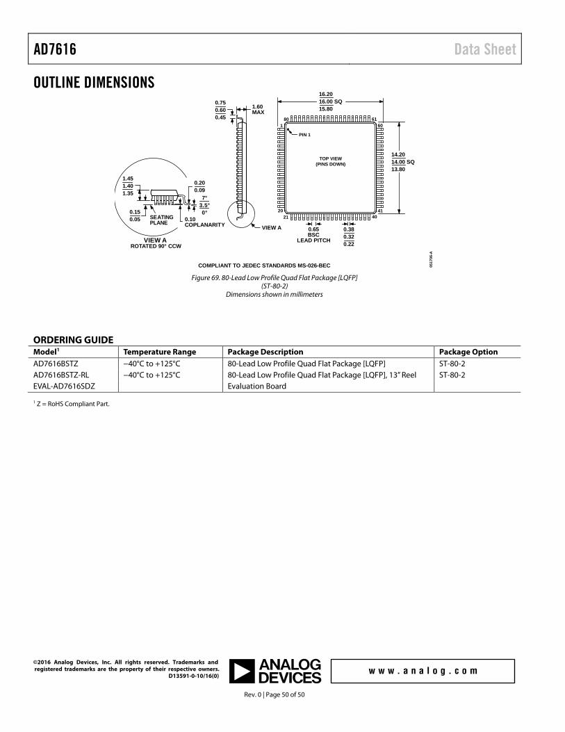
AD7616 Data Sheet
Rev. 0 | Page 50 of 50
OUTLINE DIMENSIONS
Figure 69. 80-Lead Low Profile Quad Flat Package [LQFP]
(ST-80-2) Dimensions shown in millimeters
ORDERING GUIDE Model1 Temperature Range Package Description Package Option AD7616BSTZ −40°C to +125°C 80-Lead Low Profile Quad Flat Package [LQFP] ST-80-2 AD7616BSTZ-RL −40°C to +125°C 80-Lead Low Profile Quad Flat Package [LQFP], 13” Reel ST-80-2 EVAL-AD7616SDZ Evaluation Board 1 Z = RoHS Compliant Part.
COMPLIANT TO JEDEC STANDARDS MS-026-BEC
1.45 1.40 1.35
0.150.05
0.200.09
0.10COPLANARITY
VIEW AROTATED 90° CCW
SEATINGPLANE
7°3.5°0°
61601
80
20 4121 40
VIEW A
1.60MAX
0.750.600.45
16.2016.00 SQ15.80
14.2014.00 SQ13.80
0.65BSC
LEAD PITCH
0.380.320.22
TOP VIEW(PINS DOWN)
PIN 1
0517
06-A
©2016 Analog Devices, Inc. All rights reserved. Trademarks and registered trademarks are the property of their respective owners. D13591-0-10/16(0)
![DC-to-DC Switching-Regulator Insights—Achieving Longer ... · By Sridhar Gurram [sridhar.gurram@analog.com] Oliver Brennan [oliver.brennan@analog.com] Tim Wilkerson [tim.wilkerson@analog.com]](https://static.fdocuments.net/doc/165x107/61219f3deb944c100772c8e6/dc-to-dc-switching-regulator-insightsaachieving-longer-by-sridhar-gurram-sridhargurram.jpg)