
AD6634 80 MSPS, Dual-Channel WCDMA Receive Signal ... · 80 MSPS, Dual-Channel WCDMA Receive Signal...
52
REV. 0 a Information furnished by Analog Devices is believed to be accurate and reliable. However, no responsibility is assumed by Analog Devices for its use, nor for any infringements of patents or other rights of third parties that may result from its use. No license is granted by implication or otherwise under any patent or patent rights of Analog Devices. One Technology Way, P.O. Box 9106, Norwood, MA 02062-9106, U.S.A. Tel: 781/329-4700 www.analog.com Fax: 781/326-8703 © Analog Devices, Inc., 2002 AD6634 80 MSPS, Dual-Channel WCDMA Receive Signal Processor (RSP) FEATURES 80 MSPS Wideband Inputs (14 Linear Bits Plus Three RSSI) Processes Two WCDMA Channels (UMTS or CDMA2000 1) or Four GSM/EDGE, IS136 Channels Four Independent Digital Receivers in a Single Package Dual 16-Bit Parallel Output Ports Dual 8-Bit Link Ports Programmable Digital AGC Loops with 96 dB Range Digital Resampling for Noninteger Decimation Rates Programmable Decimating FIR Filters Interpolating Half-Band Filters Programmable Attenuator Control for Clip Prevention and External Gain Ranging via Level Indicator Flexible Control for Multicarrier and Phased Array 3.3 V I/O, 2.5 V CMOS Core User Configurable Built-In Self-Test (BIST) Capability JTAG Boundary Scan FUNCTIONAL BLOCK DIAGRAM I N P U T M A T R I X rCIC2 RESAMPLER CIC5 RAM COEFFICIENT FILTER CHANNEL 0 NCO RCF OUTPUTS CHANNELS 0, 1, 2, 3 PORT B LINK PORT OR PARALLEL PORT INA[13:0] EXPA[2:0] IENA LIA-A LIA-B INB[13:0] EXPB[2:0] LIB-A LIB-B IENB SYNCA SYNCB SYNCC SYNCD EXTERNAL SYNC. CIRCUIT rCIC2 RESAMPLER CIC5 RAM COEFFICIENT FILTER CHANNEL 1 NCO rCIC2 RESAMPLER CIC5 RAM COEFFICIENT FILTER CHANNEL 2 NCO rCIC2 RESAMPLER CIC5 RAM COEFFICIENT FILTER CHANNEL 3 NCO JTAG BUILT-IN (BIST) SELF-TEST CIRCUITRY MICROPORT OR SERIAL PORT CONTROL RCF OUTPUTS CHANNELS 0, 1, 2, 3 PORT A LINK PORT OR PARALLEL PORT OUTPUT MUX CIRCUITRY INTERPOLATING HALF-BAND FILTER PLUS DIGITAL AGC INTERPOLATING HALF-BAND FILTER PLUS DIGITAL AGC APPLICATIONS Multicarrier, Multimode Digital Receivers GSM, IS136, EDGE, PHS, IS95, UMTS, CDMA2000 Micro and Pico Cell Systems, Software Radios Wireless Local Loop Smart Antenna Systems In Building Wireless Telephony
-
Upload
vuongkhanh -
Category
Documents
-
view
233 -
download
0
Transcript of AD6634 80 MSPS, Dual-Channel WCDMA Receive Signal ... · 80 MSPS, Dual-Channel WCDMA Receive Signal...

REV. 0
a
Information furnished by Analog Devices is believed to be accurate andreliable. However, no responsibility is assumed by Analog Devices for itsuse, nor for any infringements of patents or other rights of third parties thatmay result from its use. No license is granted by implication or otherwiseunder any patent or patent rights of Analog Devices.
One Technology Way, P.O. Box 9106, Norwood, MA 02062-9106, U.S.A.
Tel: 781/329-4700 www.analog.com
Fax: 781/326-8703 © Analog Devices, Inc., 2002
AD6634
80 MSPS, Dual-Channel WCDMAReceive Signal Processor (RSP)
FEATURES
80 MSPS Wideband Inputs (14 Linear Bits Plus Three
RSSI)
Processes Two WCDMA Channels (UMTS or CDMA2000
1) or Four GSM/EDGE, IS136 Channels
Four Independent Digital Receivers in a Single Package
Dual 16-Bit Parallel Output Ports
Dual 8-Bit Link Ports
Programmable Digital AGC Loops with 96 dB Range
Digital Resampling for Noninteger Decimation Rates
Programmable Decimating FIR Filters
Interpolating Half-Band Filters
Programmable Attenuator Control for Clip Prevention
and External Gain Ranging via Level Indicator
Flexible Control for Multicarrier and Phased Array
3.3 V I/O, 2.5 V CMOS Core
User Configurable Built-In Self-Test (BIST) Capability
JTAG Boundary Scan
FUNCTIONAL BLOCK DIAGRAM
INPUT
MATRIX
rCIC2RESAMPLER
CIC5RAM
COEFFICIENTFILTER
CHANNEL 0
NCO
RCF OUTPUTSCHANNELS 0, 1, 2, 3
PORT B
LINK PORTOR
PARALLELPORT
INA[13:0]EXPA[2:0]
IENA
LIA-A
LIA-B
INB[13:0]EXPB[2:0]
LIB-A
LIB-B
IENB
SYNCA
SYNCB
SYNCC
SYNCD
EXTERNALSYNC.
CIRCUIT
rCIC2RESAMPLER
CIC5RAM
COEFFICIENTFILTER
CHANNEL 1
NCO
rCIC2RESAMPLER
CIC5RAM
COEFFICIENTFILTER
CHANNEL 2
NCO
rCIC2RESAMPLER
CIC5RAM
COEFFICIENTFILTER
CHANNEL 3
NCO
JTAG BUILT-IN (BIST)SELF-TEST CIRCUITRY
MICROPORT OR SERIALPORT CONTROL
RCF OUTPUTSCHANNELS 0, 1, 2, 3
PORT A
LINK PORTOR
PARALLELPORT
OUTPUTMUX
CIRCUITRY
INTERPOLATINGHALF-BAND FILTER
PLUSDIGITAL AGC
INTERPOLATINGHALF-BAND FILTER
PLUSDIGITAL AGC
APPLICATIONS
Multicarrier, Multimode Digital Receivers
GSM, IS136, EDGE, PHS, IS95, UMTS, CDMA2000
Micro and Pico Cell Systems, Software Radios
Wireless Local Loop
Smart Antenna Systems
In Building Wireless Telephony

REV. 0–2–
AD6634TABLE OF CONTENTS
USER CONFIGURABLE BUILT-IN SELF TEST (BIST) 31RAM BIST . . . . . . . . . . . . . . . . . . . . . . . . . . . . . . . . . . . 31Channel BIST . . . . . . . . . . . . . . . . . . . . . . . . . . . . . . . . . 31
CHIP SYNCHRONIZATION . . . . . . . . . . . . . . . . . . . . . . 32Start . . . . . . . . . . . . . . . . . . . . . . . . . . . . . . . . . . . . . . . . . 32Start with No Sync . . . . . . . . . . . . . . . . . . . . . . . . . . . . . . 32Start with Soft Sync . . . . . . . . . . . . . . . . . . . . . . . . . . . . . 32Start with Pin Sync . . . . . . . . . . . . . . . . . . . . . . . . . . . . . 32Hop . . . . . . . . . . . . . . . . . . . . . . . . . . . . . . . . . . . . . . . . . 32Set Freq No Hop . . . . . . . . . . . . . . . . . . . . . . . . . . . . . . . 33Hop with Soft Sync . . . . . . . . . . . . . . . . . . . . . . . . . . . . . 33Hop with Pin Sync . . . . . . . . . . . . . . . . . . . . . . . . . . . . . . 33
PARALLEL OUTPUT PORTS . . . . . . . . . . . . . . . . . . . . . 33Channel Mode . . . . . . . . . . . . . . . . . . . . . . . . . . . . . . . . . 33AGC Mode . . . . . . . . . . . . . . . . . . . . . . . . . . . . . . . . . . . 34Master/Slave PCLK Modes . . . . . . . . . . . . . . . . . . . . . . . 35Parallel Port Pin Functionality . . . . . . . . . . . . . . . . . . . . . 35
LINK PORT . . . . . . . . . . . . . . . . . . . . . . . . . . . . . . . . . . . . 35Link Port Data Format . . . . . . . . . . . . . . . . . . . . . . . . . . 35Link Port Timing . . . . . . . . . . . . . . . . . . . . . . . . . . . . . . . 36TigerSHARC Configuration . . . . . . . . . . . . . . . . . . . . . . 36
MEMORY MAPS . . . . . . . . . . . . . . . . . . . . . . . . . . . . . . . . 360x00–0x7F: Coefficient Memory (CMEM) . . . . . . . . . . . 360x80: Channel Sleep Register . . . . . . . . . . . . . . . . . . . . . . 370x81: Soft_SYNC Register . . . . . . . . . . . . . . . . . . . . . . . . 370x82: Pin_SYNC Register . . . . . . . . . . . . . . . . . . . . . . . . 370x83: Start Hold-Off Counter . . . . . . . . . . . . . . . . . . . . . 370x84: NCO Frequency Hold-Off Counter . . . . . . . . . . . . 370x85: NCO Frequency Register 0 . . . . . . . . . . . . . . . . . . 370x86: NCO Frequency Register 1 . . . . . . . . . . . . . . . . . . 380x87: NCO Phase Offset Register . . . . . . . . . . . . . . . . . . 380x88: NCO Control Register . . . . . . . . . . . . . . . . . . . . . . 380x90: rCIC2 Decimation–1 (MrCIC2–1) . . . . . . . . . . . . . . 390x91: rCIC2 Interpolation–1 (LrCIC2–1) . . . . . . . . . . . . . . 390x92: rCIC2 Scale . . . . . . . . . . . . . . . . . . . . . . . . . . . . . . 390x93: . . . . . . . . . . . . . . . . . . . . . . . . . . . . . . . . . . . . . . . . 400x94: CIC5 Decimation–1 (MCIC5–1) . . . . . . . . . . . . . . . 400x95: CIC5 Scale . . . . . . . . . . . . . . . . . . . . . . . . . . . . . . . 400x96: . . . . . . . . . . . . . . . . . . . . . . . . . . . . . . . . . . . . . . . . 400xA0: RCF Decimation–1 (MRCF–1) . . . . . . . . . . . . . . . . 400xA1: RCF Decimation Phase (PRCF) . . . . . . . . . . . . . . . 400xA2: RCF Number of Taps Minus One (NRCF–1) . . . . . 400xA3: RCF Coefficient Offset (CORCF) . . . . . . . . . . . . . . 400xA4: RCF Control Register . . . . . . . . . . . . . . . . . . . . . . 400xA5: BIST Register for I . . . . . . . . . . . . . . . . . . . . . . . . 400xA6: BIST Register for Q . . . . . . . . . . . . . . . . . . . . . . . . 400xA7: BIST Control Register . . . . . . . . . . . . . . . . . . . . . . 410xA8: RAM BIST Control Register . . . . . . . . . . . . . . . . . 410xA9: Output Control Register . . . . . . . . . . . . . . . . . . . . 41
Memory Map for Input Port Control Registers . . . . . . . . . . 41Input Port Control Registers . . . . . . . . . . . . . . . . . . . . . . 410x00 Lower Threshold A . . . . . . . . . . . . . . . . . . . . . . . . . 410x01 Upper Threshold A . . . . . . . . . . . . . . . . . . . . . . . . . 410x02 Dwell Time A . . . . . . . . . . . . . . . . . . . . . . . . . . . . . 410x03 Gain Range A Control Register . . . . . . . . . . . . . . . . 410x04 Lower Threshold B . . . . . . . . . . . . . . . . . . . . . . . . . 420x05 Upper Threshold B . . . . . . . . . . . . . . . . . . . . . . . . . 420x06 Dwell Time B . . . . . . . . . . . . . . . . . . . . . . . . . . . . . 420x07 Gain Range B Control Register . . . . . . . . . . . . . . . . 42
FEATURES . . . . . . . . . . . . . . . . . . . . . . . . . . . . . . . . . . . . . 1APPLICATIONS . . . . . . . . . . . . . . . . . . . . . . . . . . . . . . . . . 1GENERAL DESCRIPTION . . . . . . . . . . . . . . . . . . . . . . . . . 4ARCHITECTURE . . . . . . . . . . . . . . . . . . . . . . . . . . . . . . . . 4ABSOLUTE MAXIMUM RATINGS . . . . . . . . . . . . . . . . . 6THERMAL CHARACTERISTICS . . . . . . . . . . . . . . . . . . . 6EXPLANATION OF TEST LEVELS . . . . . . . . . . . . . . . . . 6ORDERING GUIDE . . . . . . . . . . . . . . . . . . . . . . . . . . . . . . 6RECOMMENDED OPERATING CONDITIONS . . . . . . . 7ELECTRICAL CHARACTERISTICS . . . . . . . . . . . . . . . . . 7GENERAL TIMING CHARACTERISTICS . . . . . . . . . . . . 8MICROPROCESSOR PORT TIMING CHARACTERISTICS 9TIMING DIAGRAMS . . . . . . . . . . . . . . . . . . . . . . . . . . . . 10PIN CONFIGURATION . . . . . . . . . . . . . . . . . . . . . . . . . . 17PIN FUNCTION DESCRIPTIONS . . . . . . . . . . . . . . . . . 18EXAMPLE FILTER RESPONSE . . . . . . . . . . . . . . . . . . . 19INPUT DATA PORTS . . . . . . . . . . . . . . . . . . . . . . . . . . . . 20
Input Data Format . . . . . . . . . . . . . . . . . . . . . . . . . . . . . . 20Input Timing . . . . . . . . . . . . . . . . . . . . . . . . . . . . . . . . . . 20Input Enable Control . . . . . . . . . . . . . . . . . . . . . . . . . . . . 20Gain Switching . . . . . . . . . . . . . . . . . . . . . . . . . . . . . . . . . 21Input Data Scaling . . . . . . . . . . . . . . . . . . . . . . . . . . . . . . 21Scaling with Fixed-Point ADCs . . . . . . . . . . . . . . . . . . . . 21Scaling with Floating-Point or Gain-Ranging ADCs . . . . 22
NUMERICALLY CONTROLLED OSCILLATOR . . . . . 22Frequency Translation . . . . . . . . . . . . . . . . . . . . . . . . . . . 22NCO Frequency Hold-Off Register . . . . . . . . . . . . . . . . . 23Phase Offset . . . . . . . . . . . . . . . . . . . . . . . . . . . . . . . . . . . 23NCO Control Register . . . . . . . . . . . . . . . . . . . . . . . . . . . 23Bypass . . . . . . . . . . . . . . . . . . . . . . . . . . . . . . . . . . . . . . . 23Phase Dither . . . . . . . . . . . . . . . . . . . . . . . . . . . . . . . . . . 23Amplitude Dither . . . . . . . . . . . . . . . . . . . . . . . . . . . . . . . 23Clear Phase Accumulator on HOP . . . . . . . . . . . . . . . . . . 23Input Enable Control . . . . . . . . . . . . . . . . . . . . . . . . . . . . 23Mode 00: Blank on IEN Low . . . . . . . . . . . . . . . . . . . . . . 23Mode 01: Clock on IEN High . . . . . . . . . . . . . . . . . . . . . 23Mode 10: Clock on IEN Transition to High . . . . . . . . . . 24Mode 11: Clock on IEN Transition to Low . . . . . . . . . . . 24WB Input Select . . . . . . . . . . . . . . . . . . . . . . . . . . . . . . . . 24Sync Select . . . . . . . . . . . . . . . . . . . . . . . . . . . . . . . . . . . . 24
SECOND ORDER rCIC FILTER . . . . . . . . . . . . . . . . . . . 24rCIC2 Rejection . . . . . . . . . . . . . . . . . . . . . . . . . . . . . . . . 25Example Calculations . . . . . . . . . . . . . . . . . . . . . . . . . . . . 25Decimation and Interpolation Registers . . . . . . . . . . . . . . 25rCIC2 Scale . . . . . . . . . . . . . . . . . . . . . . . . . . . . . . . . . . . 25
FIFTH ORDER CIC FILTER . . . . . . . . . . . . . . . . . . . . . . 25CIC5 Rejection . . . . . . . . . . . . . . . . . . . . . . . . . . . . . . . . 26
RAM COEFFICIENT FILTER . . . . . . . . . . . . . . . . . . . . . 27RCF Decimation Register . . . . . . . . . . . . . . . . . . . . . . . . 27RCF Decimation Phase . . . . . . . . . . . . . . . . . . . . . . . . . . 27RCF Filter Length . . . . . . . . . . . . . . . . . . . . . . . . . . . . . . 27RCF Output Scale Factor and Control Register . . . . . . . . 27
INTERPOLATING HALF-BAND FILTERS . . . . . . . . . . 28AUTOMATIC GAIN CONTROL . . . . . . . . . . . . . . . . . . . 28
The AGC Loop . . . . . . . . . . . . . . . . . . . . . . . . . . . . . . . . 29Desired Signal Level Mode . . . . . . . . . . . . . . . . . . . . . . . 29Desired Clipping Level Mode . . . . . . . . . . . . . . . . . . . . . 31Synchronization . . . . . . . . . . . . . . . . . . . . . . . . . . . . . . . . 31

REV. 0
AD6634
–3–
Memory Map for Output Port Control Registers . . . . . . . . . 450x08 Port A Control Register . . . . . . . . . . . . . . . . . . . . . . 450x09 Port B Control Register . . . . . . . . . . . . . . . . . . . . . . 450x0A AGC A Control Register . . . . . . . . . . . . . . . . . . . . . 450x0B AGC A Hold-Off Counter . . . . . . . . . . . . . . . . . . . 450x0C AGC A Desired Level . . . . . . . . . . . . . . . . . . . . . . . 450x0D AGC A Signal Gain . . . . . . . . . . . . . . . . . . . . . . . . 450x0E AGC A Loop Gain . . . . . . . . . . . . . . . . . . . . . . . . . 450x0F AGC A Pole Location . . . . . . . . . . . . . . . . . . . . . . . 450x10 AGC A Average Samples . . . . . . . . . . . . . . . . . . . . . 450x11 AGC A Update Decimation . . . . . . . . . . . . . . . . . . 460x12 AGC B Control Register . . . . . . . . . . . . . . . . . . . . . 460x13 AGC B Hold-Off Counter . . . . . . . . . . . . . . . . . . . . 460x14 AGC B Desired Level . . . . . . . . . . . . . . . . . . . . . . . 460x15 AGC B Signal Gain . . . . . . . . . . . . . . . . . . . . . . . . . 460x16 AGC B Loop Gain . . . . . . . . . . . . . . . . . . . . . . . . . 460x17 AGC B Pole Location . . . . . . . . . . . . . . . . . . . . . . . 460x18 AGC B Average Samples . . . . . . . . . . . . . . . . . . . . . 460x19 AGC B Update Decimation . . . . . . . . . . . . . . . . . . 460x1A Parallel Port Control A . . . . . . . . . . . . . . . . . . . . . . 460x1B Link Port Control A . . . . . . . . . . . . . . . . . . . . . . . . 470x1C Parallel Port Control B . . . . . . . . . . . . . . . . . . . . . . 470x1D Link Port Control B . . . . . . . . . . . . . . . . . . . . . . . . 470x1E Port Clock Control . . . . . . . . . . . . . . . . . . . . . . . . . 47
MICROPORT CONTROL . . . . . . . . . . . . . . . . . . . . . . . . 48External Memory Map . . . . . . . . . . . . . . . . . . . . . . . . . . . 48Access Control Register (ACR) . . . . . . . . . . . . . . . . . . . . 48Microport Instructions . . . . . . . . . . . . . . . . . . . . . . . . . . . 48Channel Address Register (CAR) . . . . . . . . . . . . . . . . . . . 49SOFT_SYNC Control Register . . . . . . . . . . . . . . . . . . . . 49PIN_SYNC Control Register . . . . . . . . . . . . . . . . . . . . . . 49SLEEP Control Register . . . . . . . . . . . . . . . . . . . . . . . . . 49Data Address Registers . . . . . . . . . . . . . . . . . . . . . . . . . . 49Write Sequencing . . . . . . . . . . . . . . . . . . . . . . . . . . . . . . . 50Read Sequencing . . . . . . . . . . . . . . . . . . . . . . . . . . . . . . . 50Read/Write Chaining . . . . . . . . . . . . . . . . . . . . . . . . . . . . 50Intel Nonmultiplexed Mode (INM) . . . . . . . . . . . . . . . . . 50Motorola Nonmultiplexed Mode (MNM) . . . . . . . . . . . . 50
SERIAL PORT CONTROL . . . . . . . . . . . . . . . . . . . . . . . . 50Serial Port Timing Specifications . . . . . . . . . . . . . . . . . . . 50SDI . . . . . . . . . . . . . . . . . . . . . . . . . . . . . . . . . . . . . . . . . 50SCLK . . . . . . . . . . . . . . . . . . . . . . . . . . . . . . . . . . . . . . . 50
JTAG BOUNDARY SCAN . . . . . . . . . . . . . . . . . . . . . . . . 51INTERNAL WRITE ACCESS . . . . . . . . . . . . . . . . . . . . . . 51
Write Pseudocode . . . . . . . . . . . . . . . . . . . . . . . . . . . . . . 51INTERNAL READ ACCESS . . . . . . . . . . . . . . . . . . . . . . . 52
Read Pseudocode . . . . . . . . . . . . . . . . . . . . . . . . . . . . . . . 52OUTLINE DIMENSIONS . . . . . . . . . . . . . . . . . . . . . . . . . 52
TABLE OF CONTENTS (continued)

REV. 0–4–
AD6634GENERAL DESCRIPTIONThe AD6634 is a multimode 4-channel digital receive signal pro-cessor (RSP) capable of processing up to two WCDMA channels.Each channel consists of four cascaded signal processing elements:a frequency translator, two fixed coefficient decimating filters,and a programmable coefficient decimating filter. Each input porthas input level threshold detection circuitry and an AGC con-troller for accommodating large dynamic ranges or situationswhere gain ranging converters are used. Dual 16-bit parallel outputports accommodate high data rate WBCDMA applications. On-chipinterpolating half-band can also be used to further increase theoutput rate. In addition, each parallel output port has a digitalAGC for output data scaling. Link port outputs are provided toenable glueless interfaces to ADI’s TigerSHARC® DSP core.
The AD6634 is part of Analog Devices’ SoftCell® Multicarriertransceiver chipset designed for compatibility with Analog Devices’family of high sample rate IF sampling ADCs (AD9238/AD664512- and 14-bit). The SoftCell receiver comprises a digital receivercapable of digitizing an entire spectrum of carriers and digitallyselecting the carrier of interest for tuning and channel selection.This architecture eliminates redundant radios in wireless basestation applications.
High dynamic range decimation filters offer a wide range ofdecimation rates. The RAM-based architecture allows easyreconfiguration for multimode applications.
The decimating filters remove unwanted signals and noise fromthe channel of interest. When the channel of interest occupies lessbandwidth than the input signal, this rejection of out-of-bandnoise is called processing gain. By using large decimation factors,this processing gain can improve the SNR of the ADC by 30 dBor more. In addition, the programmable RAM coefficient filterallows antialiasing, matched filtering, and static equalization func-tions to be combined in a single, cost-effective filter. Half-bandinterpolating filters at the output are used in WCDMA applicationsto increase the output rate from 2× to 4× of the chip rate. TheAD6634 is also equipped with two independent automatic gaincontrol (AGC) loops for direct interface to a RAKE receiver.
The AD6634 is compatible with standard ADC converters suchas the AD664x, AD923x, AD943x, and the AD922x families ofdata converters. The AD6634 is also compatible with the AD6600diversity ADC, providing a cost and size reduction path.
*TigerSHARC and SoftCell are registered trademarks of Analog Devices, Inc.
ARCHITECTUREThe AD6634 has four signal processing stages: a frequencytranslator, second order resampling cascaded integrator combFIR filters (rCIC2), a fifth order cascaded integrator comb FIRfilter (CIC5), and a RAM coefficient FIR filter (RCF). Multiplemodes are supported for clocking data into and out of the chipand provide flexibility for interfacing to a wide variety of digitizers.Programming and control are accomplished via serial and/ormicroprocessor interfaces.
Frequency translation is accomplished with a 32-bit, complex,numerically controlled oscillator (NCO). Real data entering thisstage is separated into inphase (I) and quadrature (Q) components.This stage translates the input signal from a digital intermediatefrequency (IF) to digital baseband. Phase and amplitude dithermay be enabled on-chip to improve spurious performance of theNCO. A phase-offset word is available to create a known phaserelationship among multiple AD6634s or between channels.
Following frequency translation is a resampling, fixed coefficient,high speed, second order, resampling cascade integrator comb(rCIC2) filter that reduces the sample rate based on the ratiobetween the decimation and interpolation registers.
The next stage is a fifth order cascaded integrator comb (CIC5)filter whose response is defined by the decimation rate. The purposeof this filter is to reduce the data rate to the final filter stage sothat it can calculate more taps per output.
The final stage is a sum-of-products FIR filter with program-mable 20-bit coefficients, and decimation rates programmablefrom 1 to 256 (1–32 in practice). The RAM coefficient FIR filter(RCF in the Functional Block Diagram) can handle a maximumof 160 taps.
The next stage is a fixed coefficient half-band interpolation filterwhere data from different channels is combined together andinterpolated by a factor of 2. Next, an AGC section with a gainrange of 96.3 dB is available. This AGC section is completelyprogrammable in terms of its response. Two each of half-bandfilters and AGCs are present in the AD6634, as shown in theFunctional Block Diagram. These half-band filters and AGCsections can be bypassed independent of each other.
The overall filter response for the AD6634 is the composite of alldecimating and interpolating stages. Each successive filter stage iscapable of narrower transition bandwidths but requires a greaternumber of CLK cycles to calculate the output. More decimationin the first filter stage will minimize overall power consumption.Data from the chip is interfaced to the DSP via either a highspeed parallel port or a TigerSHARC compatible link port.
Figure 1a illustrates the basic function of the AD6634: to select andfilter a single channel from a wide input spectrum. The frequencytranslator tunes the desired carrier to baseband. Figure 1b showsthe combined filter response of the rCIC2, CIC5, and RCF.

REV. 0
AD6634
–5–
–fS/2 –3fS/8 –5fS/16 –fS/4 –3fS/16 –fS/8 –fS/16 dc fS/16 fS/8 3fS/16 fS/4 5fS/16 3fS/8 fS/2
FREQUENCY TRANSLATION (e.g., SINGLE 1MHz CHANNEL TUNED TO BASEBAND)
AFTER FREQUENCY TRANSLATION NCO “TUNES” SIGNAL TO BASEBAND
–fS/2 –3fS/8 –5fS/16 –fS/4 –3fS/16 –fS/8 –fS/16 dc fS/16 fS/8 3fS/16 fS/4 5fS/16 3fS/8 fS/2
SIGNAL OF INTEREST “IMAGE” SIGNAL OF INTEREST
WIDEBAND INPUT SPECTRUM (fSAMPLE/2 TO fSAMPLE/2)
WIDEBAND INPUT SPECTRUM (e.g., 30MHz FROM HIGH SPEED ADC)
Figure 1a. Frequency Translation of Wideband Input Spectrum
–1.5104
kHz
20
dB
c
0
–20
–40
–60
–80
–100
–120–1.0104 –5000 0 5000 1.0104 1.5104
Figure 1b. Composite Filter Response of rCIC2, CIC5, and RCF
REV. 0–6–
AD6634
CAUTIONESD (electrostatic discharge) sensitive device. Electrostatic charges as high as 4000 V readilyaccumulate on the human body and test equipment and can discharge without detection. Although theAD6634 features proprietary ESD protection circuitry, permanent damage may occur on devicessubjected to high energy electrostatic discharges. Therefore, proper ESD precautions are recommendedto avoid performance degradation or loss of functionality.
WARNING!
ESD SENSITIVE DEVICE
ABSOLUTE MAXIMUM RATINGS*
Supply Voltage . . . . . . . . . . . . . . . . . . . . . . . . . . . . . . . . . 3.6 VInput Voltage . . . . . . . . . . . . –0.3 V to +5.3 V (5 V Tolerant)Output Voltage Swing . . . . . . . . . . –0.3 V to VDDIO +0.3 VLoad Capacitance . . . . . . . . . . . . . . . . . . . . . . . . . . . . 200 pFJunction Temperature Under Bias . . . . . . . . . . . . . . . . . 125°CStorage Temperature Range . . . . . . . . . . . . –65°C to +150°CLead Temperature (5 sec) . . . . . . . . . . . . . . . . . . . . . . 280°C
*Stresses greater than those listed under Absolute Maximum Ratings may causepermanent damage to the device. These are stress ratings only; functionaloperation of the devices at these or any other conditions greater than thoseindicated in the operational sections of this specification is not implied. Exposureto absolute maximum rating conditions for extended periods may affect devicereliability.
ORDERING GUIDE
Model Temperature Range Package Description Package Option
AD6634BBC –40°C to +85°C (Ambient) 196-Lead CSPBGA (Ball Grid Array) BC-196AD6634BC/PCB Evaluation Board with AD6634 and Software
THERMAL CHARACTERISTICS196-Lead BGA:
JA = 41°C/W, No AirflowJA = 39°C/W, 200-lfpm AirflowJA = 37°C/W, 400-lfpm Airflow
Thermal measurements made in the horizontal position on a4-layer board.
EXPLANATION OF TEST LEVELSI. 100% Production Tested.II. 100% Production Tested at 25°C, and Sampled Tested at
Specified Temperatures.III. Sample Tested OnlyIV. Parameter Guaranteed by Design and AnalysisV. Parameter is Typical Value OnlyVI. 100% Production Tested at 25°C, and Sampled Tested at
Temperature Extremes

REV. 0
AD6634
–7–
SPECIFICATIONSRECOMMENDED OPERATING CONDITIONS
Test AD6634BBCParameter Temp Level Min Typ Max Unit
VDD IV 2.25 2.5 2.75 VVDDIO IV 3.0 3.3 3.6 VTAMBIENT IV –40 +25 +85 °C
ELECTRICAL CHARACTERISTICSTest AD6634BBC
Parameter (Conditions) Temp Level Min Typ Max Unit
LOGIC INPUTS (5 V Tolerant)Logic Compatibility Full IV 3.3 CMOS VLogic “1” Voltage Full IV 2.0 5.0 VLogic “0” Voltage Full IV –0.3 +0.8 VLogic “1” Current Full IV 1 10 µALogic “0” Current Full IV 1 10 µALogic “1” Current (Inputs with Pull-Down) Full IVLogic “0” Current (Inputs with Pull-Up) Full IVInput Capacitance 25°C V 4 pF
LOGIC OUTPUTSLogic Compatibility Full IV 3.3 CMOS/TTL VLogic “1” Voltage (IOH = 0.25 mA) Full IV 2.4 VDD–0.2 VLogic “0” Voltage (IOL = 0.25 mA) Full IV 0.2 0.4 V
IDD SUPPLY CURRENTCLK = 80 MHz, (VDD = 2.75 V, VDDIO = 3.6 V) Full IV
IVDD 397 443 mAIVDDIO 50 58 mA
CLK = GSM Example (65 MSPS, VDD = 2.5 V,VDDIO = 3.3 V, Dec = 2/10/6 120 TapsFour Channels) 25°C V
IVDD TBD mAIVDDIO TBD mA
CLK = WBCDMA Example (76.8 MSPS,VDD = 2.5 V, VDDIO = 3.3 V, Dec = 2/10/6120 Taps Four Channels) 25°C V
IVDD TBD mAIVDDIO TBD mA
POWER DISSIPATIONCLK = 80 MHz Full IV 1.05 1.45 WCLK = 65 MHz GSM/EDGE Example V 840 mWCLK = 76.8 MHz WBCDMA Example V 1.2 WSleep Mode Full IV 287 µW
Specifications subject to change without notice.

REV. 0–8–
AD6634
GENERAL TIMING CHARACTERISTICS1, 2
Test AD6634BBCParameter (Conditions) Temp Level Min Typ Max Unit
CLK TIMING REQUIREMENTStCLK CLK Period Full I 12.5 nstCLKL CLK Width Low Full IV 5.6 0.5 × tCLK nstCLKH CLK Width High Full IV 5.6 0.5 × tCLK ns
RESET TIMING REQUIREMENTStRESL RESET Width Low Full I 30.0 ns
INPUT WIDEBAND DATA TIMING REQUIREMENTStSI Input to ↑CLK Setup Time Full IV 2.0 nstHI Input to ↑CLK Hold Time Full IV 1.0 ns
LEVEL INDICATOR OUTPUT SWITCHING CHARACTERISTICStDLI ↑CLK to LI (A–A, B; B–A, B) Output Delay Time Full IV 3.3 10.0 ns
SYNC TIMING REQUIREMENTStSS SYNC (A, B, C, D) to ↑CLK Setup Time Full IV 2.0 nstHS SYNC (A, B, C, D) to ↑CLK Hold Time Full IV 1.0 ns
SERIAL PORT CONTROL TIMING REQUIREMENTSSWITCHING CHARACTERISTICS2
tSCLK SCLK Period Full IV 16 nstSCLKL SCLK Low Time Full IV 3.0 nstSCLKH SCLK High Time Full IV 3.0 ns
INPUT CHARACTERISTICStSSI SDI to ↓SCLK Setup Time Full IV 1.0 nstHSI SDI to ↓SCLK Hold Time Full IV 1.0 ns
PARALLEL PORT TIMING REQUIREMENTS (MASTER MODE)SWITCHING CHARACTERISTICS3
tDPOCLKL ↓CLK to ↑PCLK Delay (Divide by 1) Full IV 6.5 10.5 nstDPOCLKLL ↓CLK to ↑PCLK Delay (Divide by 2, 4, or 8) Full IV 8.3 14.6 nstDPREQ ↑CLK to ↑PxREQ Delay 1.0 nstDPP ↑CLK to Px[15:0] Delay 0.0 ns
INPUT CHARACTERISTICStSPA PxACK to ↓PCLK Setup Time +7.0 nstHPA PxACK to ↓PCLK Hold Time –3.0 ns
PARALLEL PORT TIMING REQUIREMENTS (SLAVE MODE)SWITCHING CHARACTERISTICS3
tPOCLK PCLK Period Full I 12.5 nstPOCLKL PCLK Low Period (when PCLK Divisor = 1) Full IV 2.0 0.5 × tPOCLK nstPOCLKH PCLK High Period (when PCLK Divisor = 1) Full IV 2.0 0.5 × tPOCLK nstDPREQ ↑CLK to ↑PxREQ Delay 10.0 nstDPP ↑CLK to Px[15:0] Delay 11.0 ns
INPUT CHARACTERISTICStSPA PxACK to ↓PCLK Setup Time 1.0 nstHPA PxACK to ↓PCLK Hold Time 1.0 ns
LINK PORT TIMING REQUIREMENTSSWITCHING CHARACTERISTICS3
tRDLCLK ↑PCLK to ↑LxCLKOUT Delay Full IV 2.5 nstFDLCLK ↓PCLK to ↓LxCLKOUT Delay Full IV 0 nstRLCLKDAT ↑LCLKOUT to Lx[7:0] Delay Full IV 0 2.9 nstFLCLKDAT ↓LCLKOUT to Lx[7:0] Delay Full IV 0 2.2 ns
NOTES1All Timing Specifications valid over VDD range of 2.25 V to 2.75 V and VDDIO range of 3.0 V to 3.6 V.2CLOAD = 40 pF on all outputs unless otherwise specified3The timing parameters for Px[15:0], PxREQ, PxACK, LxCLKOUT, Lx[7:0] apply for port A and B (x stands for A or B).
Specifications subject to change without notice.

REV. 0
AD6634
–9–
MICROPROCESSOR PORT TIMING CHARACTERISTICS1, 2
Test AD6634BBCParameter (Conditions) Temp Level Min Typ Max Unit
MICROPROCESSOR PORT, MODE INM (MODE = 0)
MODE INM WRITE TIMINGtSC Control3 to ↑CLK Setup Time Full IV 2.0 nstHC Control3 to ↑CLK Hold Time Full IV 2.5 nstHWR WR(RW) to RDY(DTACK) Hold Time Full IV 7.0 nstSAM Address/Data to WR(RW) Setup Time Full IV 3.0 nstHAM Address/Data to RDY(DTACK) Hold Time Full IV 5.0 nstDRDY WR(RW) to RDY(DTACK) Delay Full IV 8.0 nstACC WR(RW) to RDY(DTACK) High Delay Full IV 4 × tCLK 5 × tCLK 9 × tCLK ns
MODE INM READ TIMINGtSC Control3 to ↑CLK Setup Time Full IV 5.0 nstHC Control3 to ↑CLK Hold Time Full IV 2.0 nstSAM Address to RD(DS) Setup Time Full IV 0.0 nstHAM Address to Data Hold Time Full IV 5.0 nstDRDY RD(DS) to RDY(DTACK) Delay Full IV 8.0 nstACC RD(DS) to RDY(DTACK) High Delay Full IV 8 × tCLK 10 × tCLK 13 × tCLK ns
MICROPROCESSOR PORT, MODE MNM (MODE = 1)
MODE MNM WRITE TIMINGtSC Control3 to ↑CLK Setup Time Full IV 2.0 nstHC Control3 to ↑CLK Hold Time Full IV 2.5 nstHDS DS(RD) to DTACK(RDY) Hold Time Full IV 8.0 nstHRW RW(WR) to DTACK(RDY) Hold Time Full IV 7.0 nstSAM Address/Data to RW(WR) Setup Time Full IV 3.0 nstHAM Address/Data to RW(WR) Hold Time Full IV 5.0 nstDDTACK DS(RD) to DTACK(RDY) Delay Full IV 8.0 nstACC RW(WR) to DTACK(RDY) Low Delay Full IV 4 × tCLK 5 × tCLK 9 × tCLK ns
MODE MNM READ TIMINGtSC Control3 to ↑CLK Setup Time Full IV 5.0 nstHC Control3 to ↑CLK Hold Time Full IV 2.0 nstHDS DS(RD) to DTACK(RDY) Hold Time Full IV 8.0 nstSAM Address to DS(RD) Setup Time Full IV 0.0 nstHAM Address to Data Hold Time Full IV 5.0 nstDDTACK DS(RD) to DTACK(RDY) Delay Full IV 8.0 nstACC DS(RD) to DTACK(RDY) Low Delay Full IV 8 × tCLK 10 × tCLK 13 × tCLK ns
NOTES1All Timing Specifications valid over VDD range of 2.25 V to 2.75 V and VDDIO range of 3.0 V to 3.6 V.2CLOAD = 40 pF on all outputs, unless otherwise specified.3Specification pertains to control signals: R/W, (WR), DS (RD), CS.
Specifications subject to change without notice.

REV. 0–10–
AD6634TIMING DIAGRAMS
CLK
tDLI
tCLKL
tCLK
tCLKH
LIA–ALIA–BLIB–ALIB–B
Figure 2. Level Indicator Output Switching Characteristics
RESET
tRESL
Figure 3. RESET Timing Requirements
tSCLKH
tSCLKL
SCLK
Figure 4. SCLK Switching Characteristics
SCLK
SDI DATAn
tSSI tHSI
Figure 5. Serial Port Input Timing Characteristics
CLK
INx[13:0]EXPx[2:0]
IENx
tHItSI
Figure 6. Input Timing for A and B Channels

REV. 0
AD6634
–11–
tHStSS
CLK
SYNCASYNCBSYNCCCYNCD
Figure 7. SYNC Timing Inputs
CLK
PCLK
tDPOCLKL
Figure 8. PCLK to CLK Switching Characteristics Divide by 1
CLK
PCLK
tDPOCLKLL
tPOCLKLtPOCLKH
Figure 9. PCLK to CLK Switching Characteristics Divide by 2, 4, or 8
PCLK
PxACK
tSPA
tHPA
Figure 10. Master Mode PxACK to PCLK Setup and Hold Characteristics

REV. 0–12–
AD6634
DATA 1 DATA 2 DATA N–1 DATA N
PCLK
PxREQ
PxACK
Px[15:0]
tSPA
tDPP
tSPA
tDPP
Figure 11. Master Mode PxACK to PCLK Switching Characteristics
PCLK
DATA 1 DATA N
tDPP tDPP
tDPREQ
PxACK
PxREQ
Px[15:0]
Figure 12. Master Mode PxREQ to PCLK Switching Characteristics
tSPA
tHPA
tPOCLKL
tPOCLKH
PCLK
PxACK
Figure 13. Slave Mode PxACK to PCLK Setup and Hold Characteristics

REV. 0
AD6634
–13–
DATA 1 DATA 2 DATA N–1 DATA N
PCLK
PxREQ
PxACK
Px[15:0]
tSPA
tDPP
tSPA
tDPP
Figure 14. Slave Mode PxACK to PCLK Switching Characteristics
PCLK
DATA 1 DATA N
tDPP tDPP
tDPREQ
PxACK
PxREQ
Px[15:0]
Figure 15. Slave Mode PxREQ to PCLK Switching Characteristics
PCLK
LxCLKOUT
tRDLCLK tFDLCL
Figure 16. LxCLKOUT to PCLK Switching Characteristics

REV. 0–14–
AD6634
LxCLKOUT
LxCLKIN
Lx[7:0]
WAIT > = 6 CYCLESONE TIME CONNECTIVITY CHECK
NEXT TRANSFERACKNOWLEDGE
NEXT TRANSFERBEGINS
8 LxCLKOUT CYCLES
D0 D1 D2 D3 D4 D15 D0 D1 D2 D3
Figure 17. LxCLKIN to LxCLKOUT Data Switching Characteristics
LxCLKOUT
Lx[7:0]
tFDLCLKDAT tRDLCLKDAT
Figure 18. LxCLKOUT to Lx[7:0] Data Switching Characteristics
REV. 0
AD6634
–15–
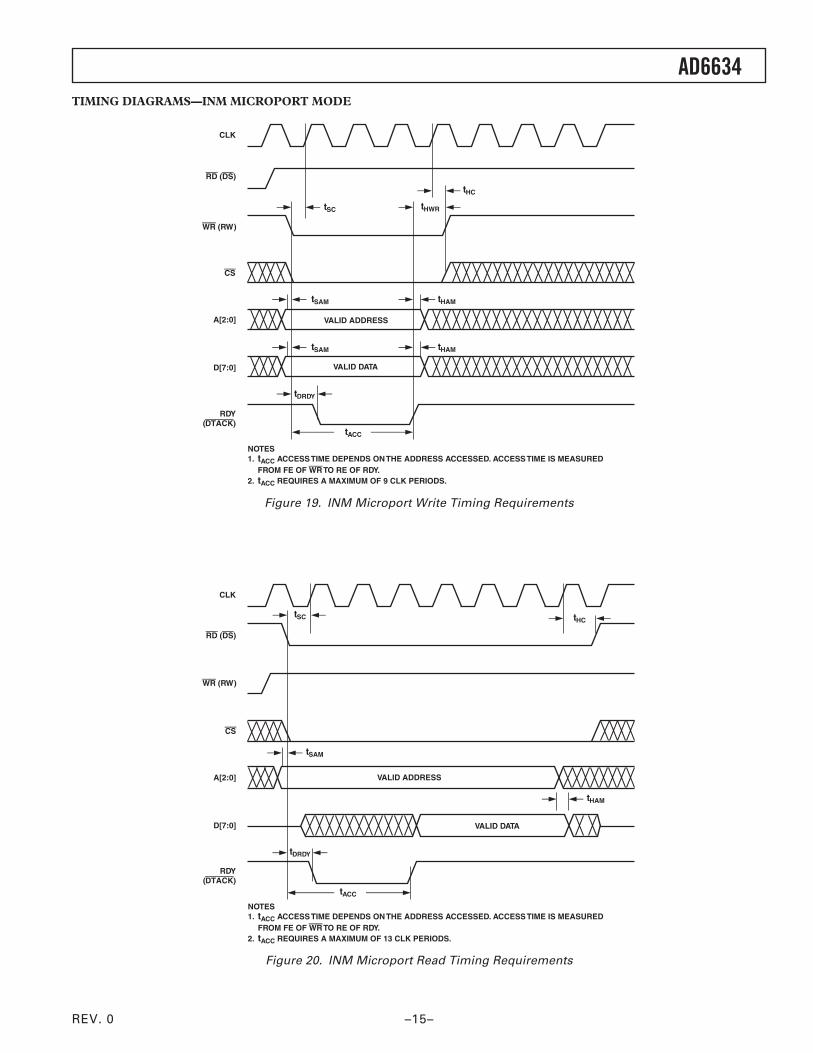
TIMING DIAGRAMS—INM MICROPORT MODE
CLK
RD (DS)
WR (RW)
CS
A[2:0]
D[7:0]
RDY(DTACK)
VALID ADDRESS
VALID DATA
NOTES1. tACC ACCESS TIME DEPENDS ON THE ADDRESS ACCESSED. ACCESS TIME IS MEASURED
FROM FE OF WR TO RE OF RDY.2. tACC REQUIRES A MAXIMUM OF 9 CLK PERIODS.
tSC
tHC
tHWR
tHAMtSAM
tHAMtSAM
tDRDY
tACC
Figure 19. INM Microport Write Timing Requirements
tSC
CLK
RD (DS)
WR (RW)
A[2:0]
D[7:0]
RDY(DTACK)
CS
NOTES1. tACC ACCESS TIME DEPENDS ON THE ADDRESS ACCESSED. ACCESS TIME IS MEASURED
FROM FE OF WR TO RE OF RDY.2. tACC REQUIRES A MAXIMUM OF 13 CLK PERIODS.
tHC
tSAM
tHAM
VALID ADDRESS
VALID DATA
tDRDY
tACC
Figure 20. INM Microport Read Timing Requirements

REV. 0–16–
AD6634TIMING DIAGRAMS—MNM MICROPORT MODE
VALID ADDRESS
VALID DATA
CLK
DS (RD)
RW (WR)
CS
A[2:0]
D[7:0]
DTACK(RDY)
NOTES1. tACC ACCESS TIME DEPENDS ON THE ADDRESS ACCESSED. ACCESS TIME IS MEASURED
FROM FE OF DS TO THE FE OF DTACK.2. tACC REQUIRES A MAXIMUM OF 9 CLK PERIODS.
tSCtHC
tHDS
tHRW
tHAM
tACC
tSAM
tHAMtSAM
tDDTACK
Figure 21. MNM Microport Write Timing Requirements
CLK
DS (RD)
RW (WR)
A[2:0]
D[7:0]
DTACK(RDY)
tSC
tACC
tDDTACK
NOTES1. tACC ACCESS TIME DEPENDS ON THE ADDRESS ACCESSED. ACCESS TIME IS MEASURED
FROM THE FE OF DS TO THE FE OF DTACK.2. tACC REQUIRES A MAXIMUM OF 13 CLK PERIODS.
VALID ADDRESS
VALID DATA
tSAM
tHC
tHDS
tHAM
CS
Figure 22. MNM Microport Read Timing Requirements

REV. 0
AD6634
–17–
PIN CONFIGURATION
1 2 3 4 5 6 7 8 9 10 11 12 13 14
1 2 3 4 5 6 7 8 9 10 11 12 13 14
A
B
C
D
E
F
G
H
J
K
L
M
N
P
A
B
C
D
E
F
G
H
J
K
L
M
N
P
1.0mm
15m
m s
q.
I/O
GROUND
BALL LEGEND
RING POWER
CORE POWER
196-LEAD BGA (15mm 15mm)TOP VIEW
NOCONNECT
INB2
INB0
LIB-B
CLK
EXPA1
INA12
INA11
INA8
INA5
INA3
INA2
INA0
NOCONNECT
INB6
INB4
INB3
INB1
IENB
EXPA0
INA13
INA9
INA6
INA4
INA1
IENA
LIB-A
LIA-A
INB9
INB5
INB7
EXPA2
INA10
INA7
LIA-B
SYNCA
INB11
INB8
INB13
DTACK(RDY)
SYNCB
SYNCC
EXPB1
INB12
INB10
VDDIO
VDD
VDDIO
VDD
VDDIO
VDD
MODE
SYNCD
RESET
VDDIO(RESERVED)
EXPB0
EXPB2
VDD
GND
GND
GND
GND
VDDIO
CS
D7
D6
PB14
PB15
PBACK
VDDIO
GND
GND
GND
GND
VDD
RW(WR)
D5
D4
PB12
PB13
PBREQ
VDD
GND
GND
GND
GND
VDD
TRST
D3
D2
PB10
PB11
PB9
VDDIO
GND
GND
GND
GND
VDD
DS(RD)
D1
D0
PB1 | LB1
PB4 | LB4
PB8
VDD
VDDIO
VDD
VDDIO
VDD
VDDIO
A1
A2
PA6 | LA6
PB2 | LB2
PB0 | LB0
A0
PCHA1 |LACLKIN
PCHA0 |LACLKOUT
PB5 | LB5
PB3 | LB3
PBIQ
PAACK
SCLK
PAREQ
TDO
TCLK
PA4 | LA4
PA5 | LA5
PA7 | LA7
PBCH1 |LBCLKIN
PBCH0 |LBCLKOUT
PCLK
SDI
CHIP_ID2
CHIP_ID0
TDI
PA14
PA12
PA10
PA8
PA2 | LA2
PA3 | LA3
NOCONNECT
PB7 | LB7
PB6 | LB6
PAIQ
CHIP_ID3
CHIP_ID1
TMS
PA15
PA13
PA11
PA9
PA0 | LA0
PA1 | LA1
NOCONNECT
A
B
C
D
E
F
G
H
J
K
L
M
N
P
A
B
C
D
E
F
G
H
J
K
L
M
N
P
1 2 3 4 5 6 7 8 9 10 11 12 13 14
1 2 3 4 5 6 7 8 9 10 11 12 13 14
REV. 0–18–
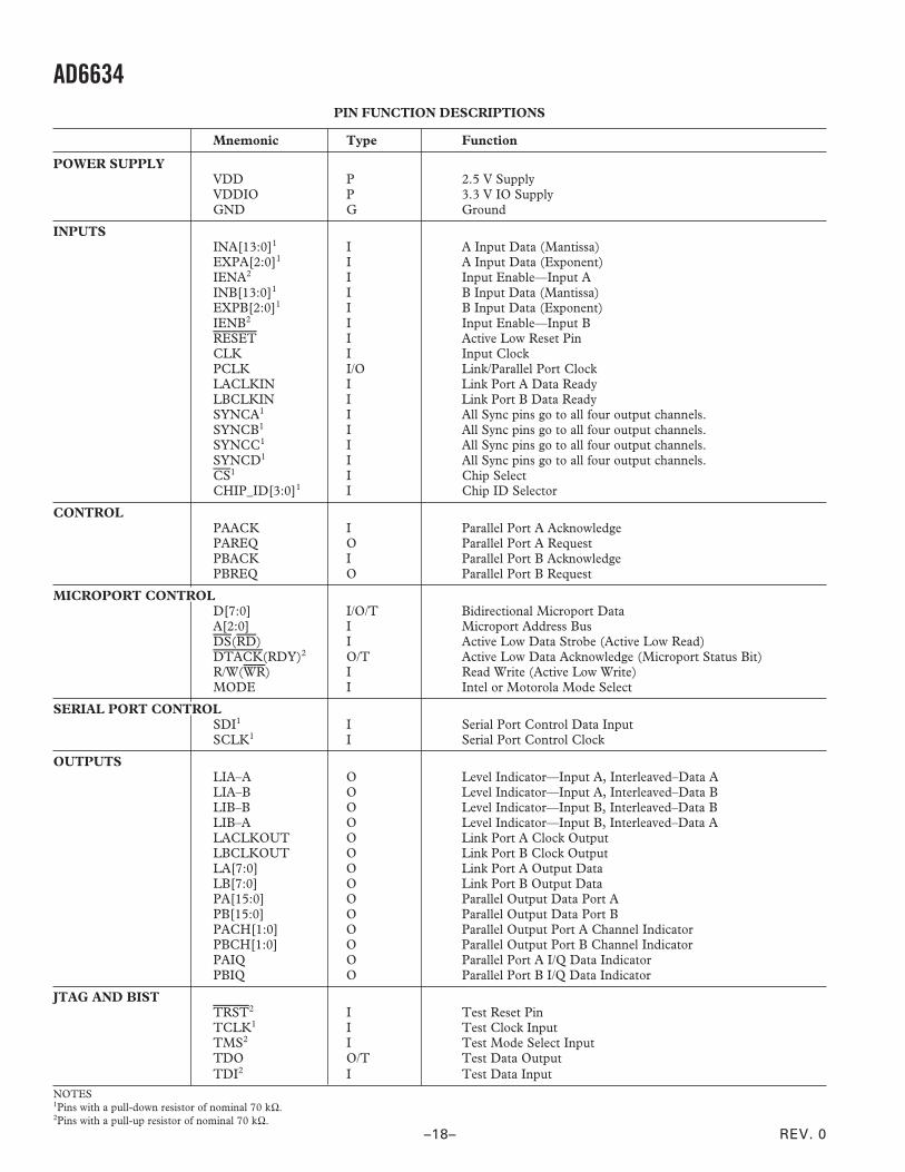
AD6634PIN FUNCTION DESCRIPTIONS
Mnemonic Type Function
POWER SUPPLYVDD P 2.5 V SupplyVDDIO P 3.3 V IO SupplyGND G Ground
INPUTSINA[13:0]1 I A Input Data (Mantissa)EXPA[2:0]1 I A Input Data (Exponent)IENA2 I Input Enable—Input AINB[13:0]1 I B Input Data (Mantissa)EXPB[2:0]1 I B Input Data (Exponent)IENB2 I Input Enable—Input BRESET I Active Low Reset PinCLK I Input ClockPCLK I/O Link/Parallel Port ClockLACLKIN I Link Port A Data ReadyLBCLKIN I Link Port B Data ReadySYNCA1 I All Sync pins go to all four output channels.SYNCB1 I All Sync pins go to all four output channels.SYNCC1 I All Sync pins go to all four output channels.SYNCD1 I All Sync pins go to all four output channels.CS1 I Chip SelectCHIP_ID[3:0]1 I Chip ID Selector
CONTROLPAACK I Parallel Port A AcknowledgePAREQ O Parallel Port A RequestPBACK I Parallel Port B AcknowledgePBREQ O Parallel Port B Request
MICROPORT CONTROLD[7:0] I/O/T Bidirectional Microport DataA[2:0] I Microport Address BusDS(RD) I Active Low Data Strobe (Active Low Read)DTACK(RDY)2 O/T Active Low Data Acknowledge (Microport Status Bit)R/W(WR) I Read Write (Active Low Write)MODE I Intel or Motorola Mode Select
SERIAL PORT CONTROLSDI1 I Serial Port Control Data InputSCLK1 I Serial Port Control Clock
OUTPUTSLIA–A O Level Indicator—Input A, Interleaved–Data ALIA–B O Level Indicator—Input A, Interleaved–Data BLIB–B O Level Indicator—Input B, Interleaved–Data BLIB–A O Level Indicator—Input B, Interleaved–Data ALACLKOUT O Link Port A Clock OutputLBCLKOUT O Link Port B Clock OutputLA[7:0] O Link Port A Output DataLB[7:0] O Link Port B Output DataPA[15:0] O Parallel Output Data Port APB[15:0] O Parallel Output Data Port BPACH[1:0] O Parallel Output Port A Channel IndicatorPBCH[1:0] O Parallel Output Port B Channel IndicatorPAIQ O Parallel Port A I/Q Data IndicatorPBIQ O Parallel Port B I/Q Data Indicator
JTAG AND BISTTRST2 I Test Reset PinTCLK1 I Test Clock InputTMS2 I Test Mode Select InputTDO O/T Test Data OutputTDI2 I Test Data Input
NOTES1Pins with a pull-down resistor of nominal 70 kΩ.2Pins with a pull-up resistor of nominal 70 kΩ.

REV. 0
AD6634
–19–
EXAMPLE FILTER RESPONSE
–1000
kHz
dB
c
–150–800 –600 –400 –200 0 200 400 600 800 1000
–140
–130
–120
–110
–100
–90
–80
–70
–60
–50
–40
–30
–20
–10
0
10
Figure 23. The Filter Above Is Based on a 65 MSPS Input Data Rate and an Output Rate of 541.6666 kSPS(Two Samples per Symbol for EDGE). Total decimation rate is 120, distributed between the rCIC2, CIC5, and RCF.
–1.0104
kHz
dB
c
–120–8000 –6000 –4000 –2000 0 2000 4000 6000 8000 1.0104
–100
–80
–60
–40
–20
0
20
CIC RESPONSE
COMPOSITE RESPONSE
DESIRED RESPONSE
Figure 24. The Filter Above Is Designed to Meet UMTS Specifications. For this configuration, the clock is set to76.8 MSPS with 20 chip rate (3.84 MCPS) and a 2 output data rate of 7.68 MCPS using two channels of the AD6634.

REV. 0–20–
AD6634INPUT DATA PORTSThe AD6634 features dual high speed ADC input ports, inputport A and input port B. The dual input ports allow for themost flexibility with a single tuner chip. These can be diversityinputs or truly independent inputs such as separate antennasegments. Either ADC port can be routed to one of four tunerchannels. For added flexibility, each input port can be used tosupport multiplexed inputs such as those found on the AD6600or other ADCs with multiplexed outputs. This added flexibilitycan allow for up to four different analog sources to be processedsimultaneously by the four internal channels.
In addition, the front end of the AD6634 contains circuitry thatenables high speed signal level detection and control. This isaccomplished with a unique high speed level detection circuitthat offers minimal latency and maximum flexibility to controlup to four analog signal paths. The overall signal path latencyfrom input to output on the AD6634 can be expressed in highspeed clock cycles. The following equation can be used tocalculate the latency.
T M M NLATENCY rCIC CIC TAPS= +( ) + +2 5 7 26
MrCIC2 and MCIC5 are decimation values for the rCIC2 and CIC5filters, respectively. NTAPS is the number RCF taps chosen.
Input Data FormatEach input port consists of a 14-bit mantissa and 3-bit exponent.If interfacing to a standard ADC is required, the exponent bits canbe grounded. If connected to a floating point ADC such as theAD6600, the exponent bits from that product can be connectedto the input exponent bits of the AD6634. The mantissa dataformat is two’s complement and the exponent is unsigned binary.
Input TimingThe data from each high speed input port is latched on therising edge of CLK. This clock signal is used to sample theinput port and clock the synchronous signal processing stagesthat follow in the selected channels.
CLK
IN[13:0]EXP[2:0] DATA
tSI
tHI
Figure 25. Input Data Timing Requirements
The clock signals can operate up to 80 MHz and have a 50% dutycycle. In applications using high speed ADCs, the ADC sampleclock or data valid strobe is typically used to clock the AD6634.
tCLKL
tCLK
tCLKH
CLK
Figure 26. CLK Timing Requirements
Input Enable ControlThere is an IENA and an IENB pin for Input Port A and InputPort B, respectively. There are four modes of operation possiblewhile using each IEN pin. Using these modes, it is possible toemulate operation of the other RSPs, such as the AD6620,which offer dual channel modes normally associated with diver-sity operations. These modes are: IEN transition to Low, IENtransition to High, IEN High, and Blank on IEN low.
In the IEN High mode, the inputs and normal operations occurwhen the input enable is high. In the IEN transition to Low mode,normal operations occur on the first rising edge of the clock afterthe IEN transitions to low. Likewise in the IEN transition to Highmode, operations occur on the rising edge of the clock after theIEN transitions to High. (See the Numerically Controlled Oscil-lator section for more details on configuring the Input EnableModes.) In Blank on IEN low mode, the input data is interpretedas zero when IEN is low.
A typical application for this feature would be to take the datafrom an AD6600 Diversity ADC to one of the inputs of theAD6634. The A/B_OUT from that chip would be tied to theIEN. Then one channel within the AD6634 would be set so thatIEN transition to Low is enabled. Another channel would beconfigured so that IEN transition to High is enabled. This wouldallow two of the AD6634 channels to be configured to emulatethat AD6620 in diversity mode. Of course the NCO frequenciesand other channel characteristics would need to be set similarly,but this feature allows the AD6634 to handle interleaved datastreams such as those found on the AD6600.
The difference between the IEN transition to high and the IENhigh is found when a system clock is provided that is higher thanthe data rate of the converter. It is often advantageous to supplya clock that runs faster than the data rate so that additional filtertaps can be computed. This naturally provides better filtering.In order to ensure that other parts of the circuit properly recog-nize the faster clock in the simplest manner, the IEN transitionto low or high should be used. In this mode, only the first clockedge that meets the setup and hold times will be used to latchand process the input data. All other clock pulses are ignored byfront end processing. However, each clock cycle will still producea new filter computation pair.

REV. 0
AD6634
–21–
Gain SwitchingThe AD6634 includes circuitry that is useful in applications whereeither large dynamic ranges exist or where gain ranging convert-ers are employed. This circuitry allows digital thresholds to beset such that an upper and a lower threshold can be programmed.
One such use of this may be to detect when an ADC is about toreach full scale with a particular input condition. The resultswould be to provide a flag that could be used to quickly insertan attenuator that would prevent ADC overdrive. If 18 dB (orany arbitrary value) of attenuation (or gain) is switched in, thesignal dynamic range of the system will have been increased by18 dB. The process begins when the input signal reaches theupper programmed threshold. In a typical application, this maybe set 1 dB (user-definable) below full scale. When this inputcondition is met, the appropriate LI (LIA-A, LIA-B, LIB-A, orLIB-B) signal associated with either the A or B input port ismade active. This can be used to switch the gain or attenuationof the external circuit. The LI line stays active until the inputcondition falls below the lower programmed threshold. In orderto provide hysteresis, a dwell time register (see Memory Map forInput Control Registers) is available to hold off switching of thecontrol line for a predetermined number of clocks. Once theinput condition is below the lower threshold, the programmablecounter begins counting high speed clocks. As long as the inputsignal stays below the lower threshold for the number of highspeed clock cycles programmed, the attenuator will be removedon the terminal count. However, if the input condition goesabove the lower threshold with the counter running, it will bereset and must fall below the lower threshold again to initiate theprocess. This will prevent unnecessary switching between statesand is illustrated in Figure 27.
When the input signal goes above the upper threshold, theappropriate LI signal becomes active. Once the signal fallsbelow the lower threshold, the counter begins counting. If theinput condition goes above the lower threshold, the counter isreset and starts again as shown in Figure 27. Once the counterhas terminated to 0, the LI line goes inactive.
“HIGH”
MA
NT
ISS
A DWELL TIME“LOW”
UPPERTHRESHOLD
LOWERTHRESHOLD
COUNTERRESTARTS
TIME
Figure 27. Threshold Settings for LI
The LI line can be used for a variety of functions. It can be usedto set the controls of an attenuator, DVGA, or integrated and usedwith an analog VGA. To simplify the use of this feature, theAD6634 includes two separate gain settings, one when this line isinactive (rCIC2_QUIET[4:0] stored in bits 9:5 of 0x92 register)and the other when active (rCIC2_LOUD[4:0] stored in bits4:0 of 0x92 register). This allows the digital gain to be adjustedto the external changes. In conjunction with the gain setting, avariable hold-off is included to compensate for the pipeline delayof the ADC and the switching time of the gain control element.Together, these two features provide seamless gain switching.
Another use of this pin is to facilitate a gain range hold-off within again ranging ADC. For converters that use gain ranging to increasetotal signal dynamic range, it may be desirable to prohibit internalgain ranging from occurring in some instances. For such converters,the LI (A or B) line can be used to hold this off. For this applica-tion, the upper threshold would be set based on similar criteria.However, the lower threshold would be set to a level consistentwith the gain ranges of the specific converter. The hold-off delaycan then be set appropriately for any of a number of factors suchas fading profile, signal peak to average ratio, or any other time-based characteristics that might cause unnecessary gain changes.
Since the AD6634 has a total of four gain control circuits thatcan be used if both A and B input ports have interleaved data.Each respective LI pin is independent and can be set to differ-ent set points. It should be noted that the gain control circuitsare wideband and are implemented prior to any filtering elementsto minimize loop delay. Any of the four channels can be set tomonitor any of the possible four input channels (two in normalmode and four when the inputs are time multiplexed).
The chip also provides appropriate scaling of the internal databased on the attenuation associated with the LI signal. In thismanner, data to the DSP maintains a correct scale value through-out the process, making it totally independent. Since there areoften finite delays associated with external gain switching com-ponents, the AD6634 includes a variable pipeline delay that canbe used to compensate for external pipeline delays or grosssettling times associated with gain/attenuator devices. This delaymay be set up to seven high speed clocks. These features ensuresmooth switching between gain settings.
Input Data ScalingThe AD6634 has two data input ports, an A input port and aB input port. Each accepts 14-bit mantissa (two’s complementinteger) IN[13:0], a 3-bit exponent (unsigned integer) EXP[2:0]and the Input Enable(IEN). Both inputs are clocked by CLK.These pins allow direct interfacing to both standard fixed-pointADCs such as the AD9238 and AD6645, as well as to gain-ranging ADCs such as the AD6600. For normal operation withADCs having fewer than 14 bits, the active bits should be MSBjustified and the unused LSBs should be tied low.
The 3-bit exponent, EXP[2:0] is interpreted as an unsignedinteger. The exponent will subsequently be modified by either ofrCIC2_LOUD[4:0] or rCIC2_QUIET[4:0] depending on whetherLI line is active or not. These 5-bit scale values are stored in therCIC2 scale register (0x92) and the scaling is applied before thedata enters the rCIC2 resampling filter. These 5-bit registerscontain scale values to compensate for the rCIC2 gain, externalattenuator (if used) and the exponent offset (Expoff). If no externalattenuator is used, both the rCIC2_QUIET and rCIC2_LOUDregisters would contain the same value. A detailed explanationand equation for setting the attenuating scale register is given inthe Scaling with Floating-Point or Gain-Ranging ADCs section.
Scaling with Fixed-Point ADCsFor fixed-point ADCs, the AD6634 exponent inputs EXP[2:0] aretypically not used and should be tied low. The ADC outputs aretied directly to the AD6634 Inputs, MSB-justified. The ExpOffbits in 0x92 should be programmed to 0. Likewise, the ExponentInvert bit should be 0. Thus for fixed-point ADCs, the exponentsare typically static and no input scaling is used in the AD6634.

REV. 0–22–
AD6634Table I. AD6600 Transfer Function with AD6634ExpInv = 1, and No ExpOff
ADC Input AD6600 AD6634 SignalLevel RSSI[2:0] Data Reduction (dB)
Largest 101 (5) /4 (>> 2) –12100 (4) /8 (>>3) –18011 (3) /16 (>> 4) –24010 (2) /32 (>> 5) –30001 (1) /64 (>> 6) –36
Smallest 000 (0) /128 (>> 7) –42
(ExpInv = 1, rCIC2 Scale = 0)
Table II. AD6600 Transfer Function with AD6620ExpInv = 1, and ExpOff = 6
ADC Input AD6600 AD6634 SignalLevel RSSI[2:0] Data Reduction (dB)
Largest 101 (5) /1 (>> 0) 0100 (4) /2 (>> 1) –6011 (3) /4 (>> 2) –12010 (2) /8 (>> 3) –18001 (1) /16 (>> 4) –24
Smallest 000 (0) /32 (>> 5) –30
(ExpInv = 1, ExpOff = 30, ExpWeight = 0)
This flexibility in handling the exponent allows the AD6634 tointerface with gain-ranging ADCs other than the AD6600. TheExponent Offset can be adjusted to allow up to seven RSSI(EXP)ranges to be used as opposed to the AD6600’s five. It also allowsthe AD6634 to be tailored in a system that employs the AD6600but does not utilize all of its signal range. For example, if onlythe first four RSSI ranges are expected to occur, the ExpOffcould be adjusted to 29, which would then make RSSI = 4correspond to the 0 dB point of the AD6634.
IN 13
IN 2
IN 1IN 0
IEN
D10 (MSB)
D0 (LSB)
AD6600 AD6634
EXP 1RSSI 1EXP 2RSSI 2
EXP 0RSSI 0AB_OUT
Figure 29. Typical Interconnection of the AD6600Gain-Ranging ADC and the AD6634
NUMERICALLY CONTROLLED OSCILLATORFrequency TranslationThis processing stage comprises a digital tuner consisting of twomultipliers and a 32-bit complex NCO. Each channel of theAD6634 has an independent NCO. The NCO serves as a quadra-ture local oscillator capable of producing an NCO frequencybetween –CLK/2 and +CLK/2 with a resolution of CLK/232 inthe complex mode. The worst-case spurious signal from theNCO is better than –100 dBc for all output frequencies.
IN 13
IN 2IN 1IN 0
EXP 2EXP 1EXP 0 IEN
VDD
D11 (MSB)
D0 (LSB)
AD6640 AD6634
Figure 28. Typical Interconnection of the AD6640Fixed Point ADC and the AD6634
Scaling with Floating-Point or Gain-Ranging ADCsAn example of the exponent control feature combines the AD6600and the AD6634. The AD6600 is an 11-bit ADC with three bitsof gain ranging. In effect, the 11-bit ADC provides the mantissa,and the three bits of relative signal strength indicator (RSSI) forthe exponent. Only five of the eight available steps are used bythe AD6600. See the AD6600 data sheet for additional details.
For gain-ranging ADCs such as the AD6600,
SCALED INPUT IN
EXPINV EXPWEIGHT
MOD EXP rCIC_ ,
,
– – ,= ×= =
+( )2
1 0
7 2 32
where, IN is the value of IN[13:0], EXP is the value ofEXP[2:0], and rCIC2 is the rCIC scale register value (0x92Bits 9–5 and 4–0).
The RSSI output of the AD6600 numerically grows with increas-ing signal strength of the analog input (RSSI = 5 for a largesignal, RSSI = 0 for a small signal). When the Exponent InvertBit (ExpInv) is set to zero, the AD6634 will consider the small-est signal at the IN[13:0] to be the largest and as the EXP wordincreases, it shifts the data down internally (EXP = 5 will shift a14-bit word right by five internal bits before passing the data tothe rCIC2). In this example where ExpInv = 0, the AD6634regards the largest signal possible on the AD6600 as the small-est signal. Thus, we can use the Exponent Invert Bit to makethe AD6634 exponent agree with the AD6600 RSSI. By settingExpInv = 1, this forces the AD6634 to shift the data up (left)for growing EXP instead of down. The exponent invert bitshould always be set high for use with the AD6600.
The exponent offset is used to shift the data up. For example,Table I shows that with no rCIC2 scaling, 12 dB of range is lostwhen the ADC input is at the largest level. This is undesirablebecause it lowers the dynamic range and SNR of the system by reduc-ing the signal of interest relative to the quantization noise floor.
To avoid this automatic attenuation of the full-scale ADC signalthe ExpOff is used to move the largest signal (RSSI = 5) up tothe point where there is no down shift. In other words, once theExponent Invert bit has been set, the exponent offset should beadjusted so that mod(7–5 + ExpOff, 32) = 0. This is the casewhen exponent offset is set to 30 since mod(32, 32) = 0.Table II illustrates the use of ExpInv and ExpOff when usedwith the AD6600 ADC.

REV. 0
AD6634
–23–
The NCO frequency value in registers 0x85 and 0x86 is interpretedas a 32-bit unsigned integer. The NCO frequency is calculatedusing the equation below.
NCO FREQ MOD
fCLK
CHANNEL_ = ×
232
where, NCO_FREQ is the 32-bit integer (registers 0x85 and 0x86),fCHANNEL is the desired channel frequency, and CLK is the AD6634master clock rate or input data rate depending on the InputEnable mode used. See Input Enable Control section.
NCO Frequency Hold-Off RegisterWhen the NCO Frequency registers are written, data is actuallypassed to a shadow register. Data may be moved to the mainregisters by one of two methods: when the channel comes out ofsleep mode or when a SYNC Hop occurs. In either event acounter can be loaded with NCO Frequency Hold-Off registervalue. The 16-bit unsigned integer counter (0x84) starts count-ing down clocked by the master clock and when it reaches zero,the new frequency value in the shadow register is written to theNCO Frequency register. The NCO could also be set up to SYNCimmediately, in which case the Frequency Hold-off counter isbypassed and new frequency values are updated immediately.
Phase OffsetThe phase offset register (0x87) adds an offset to the phaseaccumulator of the NCO. This is a 16-bit register and is inter-preted as a 16-bit unsigned integer. A 0x0000 in this registercorresponds to a 0 Radian offset and a 0xFFFF corresponds toan offset of 2 (1-1/(216)) Radians. This register allows multipleNCOs to be synchronized to produce sine waves with a knownand steady phase difference.
NCO Control RegisterThe NCO control register located at 0x88 is used to configurethe features of the NCO. These are controlled on a per-channelbasis, and are described below.
BypassThe NCO in the front end of the AD6634 can be bypassed.Bypass mode is enabled by setting Bit 0 of 0x88 high. When it isbypassed, down conversion is not performed and the AD6634channel functions simply as a real filter on complex data. This isuseful for baseband sampling applications where the A input isconnected to the I signal path within the filter and the B input isconnected to the Q signal path. This may be desired if the digi-tized signal has already been converted to baseband in prioranalog stages or by other digital preprocessing.
Phase DitherThe AD6634 provides a phase dither option for improving thespurious performance of the NCO. Phase dither is enabled bysetting Bit 1. When phase dither is enabled by setting this bithigh, spurs due to phase truncation in the NCO are randomized.The energy from these spurs is spread into the noise floor andspurious-free dynamic range is increased at the expense of veryslight decreases in the SNR. The choice of whether phasedither is used in a system will ultimately be decided by thesystem goals. It should be employed if lower spurs are desiredat the expense of a slightly raised noise floor. If a low noise flooris desired, and the higher spurs can be tolerated or filtered bysubsequent stages, phase dither is not needed.
Amplitude DitherAmplitude dither can also be used to improve spurious performanceof the NCO. Amplitude dither is enabled by setting Bit 2.
Amplitude dither improves performance by randomizing theamplitude quantization errors within the angular to Cartesianconversion of the NCO. This option may reduce spurs at theexpense of a slightly raised noise floor. Amplitude dither andphase dither can be used together, separately, or not at all.
Clear Phase Accumulator on HOPWhen Bit 3 is set, the NCO phase accumulator is cleared priorto a frequency hop. This ensures a consistent phase of the NCOon each hop. The NCO phase offset is unaffected by this settingand is still in effect. If phase continuous hopping is desired, thisbit should be cleared and the last phase in the NCO phase registerwill be the initiating point for the new frequency.
Input Enable ControlThere are four different modes of operation for the input enable.Each of the high speed input ports includes an IEN line. Any ofthe four filter channels can be programmed to take data from eitherof the two A or B input ports. (See WB Input Select section.)Along with data is the IEN(A,B) signal. Each filter channel can beconfigured to process the IEN signal in one of four modes. Threeof the modes are associated with when data is processed basedon a time division multiplexed data stream. The fourth mode isused in applications that employ time division duplex such asradar, sonar, ultrasound, and communications that involve TDD.
Mode 00: Blank on IEN LowIn this mode, data is blanked while the IEN line is low. Duringthe period of time when the IEN line is high, new data is strobedon each rising edge of the input clock. When the IEN line islowered, input data is replaced with zero values. During thisperiod, the NCO continues to run such that when the IEN lineis raised again, the NCO value will be at the value it would havebeen otherwise had the IEN line never been lowered. This modehas the effect of blanking the digital inputs when the IEN line islowered. Back end processing (rCIC2, CIC5, and RCF) continueswhile the IEN line is high. This mode is useful for time divisionmultiplexed applications.
Mode 01: Clock on IEN HighIn this mode, data is clocked into the chip while the IEN line ishigh. During the period of time when the IEN line is high, newdata is strobed on each rising edge of the input clock. Whenthe IEN line is lowered, input data is no longer latched intothe channel. Additionally, NCO advances are halted. However,back end processing (rCIC2, CIC5, and RCF) continues duringthis period. The primary use for this mode is to allow for a clockthat is faster than the input sample data rate to allow more filtertaps to be computed than would otherwise be possible. In Fig-ure 30, input data is strobed only during the period of time thatIEN is high despite the fact that the CLK continues to run at arate four times faster than the data.
n+1nIN[13:0]E[2:0]
CLK
IEN
tSI
tHI
Figure 30. Fractional Rate Input Timing (4x CLK)in Mode 01
REV. 0–24–
AD6634Mode 10: Clock on IEN Transition to HighIn this mode, data is clocked into the chip only on the first clockedge after the rising transition of the IEN line. Although data islatched only on the first valid clock edge, the back end process-ing (rCIC2, CIC5, and RCF) continues on each available clockthat may be present, similar to Mode 01. The NCO phase accu-mulator is incremented only once for each new input data sampleand not once for each input clock.
Mode 11: Clock on IEN Transition to LowIn this mode, data is clocked into the chip only on the first clockedge after the falling transition of the IEN line. Although data islatched only on the first valid clock edge, the back end process-ing (rCIC2, CIC5, and RCF) continues one each availableclock that may be present, similar to Mode 01. The NCO phaseaccumulator is incremented only once for each new input datasample and not once for each input clock.
WB Input SelectBit 6 in this register controls which input port is selected for signalprocessing. If this bit is set high, input port B (INB, EXPB, andIENB) is connected to the selected filter channel. If this bit iscleared, input port A (INA, EXPA, and IENA) is connected tothe selected filter channel.
Sync SelectBits 7 and 8 of this register determine which external sync pin isassociated with the selected channel. The AD6634 has four syncpins named SYNCA, SYNCB, SYNCC, and SYNCD. Any ofthese sync pins can be associated with any of the four receiverchannels within the AD6634. Additionally, if only one syncsignal is required for the system, all four receiver channels canreference the same sync pulse. Bit value 00 is channel A, 01 ischannel B, 10 is channel C, and 11 is channel D.
SECOND ORDER rCIC FILTERThe rCIC2 filter is a second order cascaded resampling integra-tor comb filter. The resampler is implemented using a uniquetechnique that does not require the use of a high speed clock,thus simplifying the design and saving power. The resamplerallows for noninteger relationships between the master clockand the output data rate, which allows easier implementation ofsystems that are either multimode or require a master clock thatis not a multiple of the data rate to be used.
Interpolation up to 512 and decimation up to 4096 is allowed inthe rCIC2. The resampling factor for the rCIC2 (L) is a 9-bitinteger. When combined with the decimation factor M, a 12-bitnumber, the total rate change can be any fraction in the form of:
R LM
R
rCIC
rCIC
2
2 1
=
≤
The only constraint is that the ratio L/M must be less than or equalto one. This implies that the rCIC2 decimates by 1 or more.
Resampling is implemented by apparently increasing the inputsample rate by the factor L, using zero stuffing for the new data
samples. Following the resampler is a second order cascadedintegrator comb filter. Filter characteristics are determined onlyby the fractional rate change (L/M).
The filter can process signals at the full rate of the input port,80 MHz. The output rate of this stage is given by the equation:
f
L fMSAMP
rCIC SAMP
rCIC2
2
2
=
Both LrCIC2 and MrCIC2 are unsigned integers. The interpolationrate (LrCIC2) may be from 1 to 512 and the decimation (MrCIC2)may be between 1 and 4096. The stage can be bypassed bysetting the decimation to 1/1. The frequency response of therCIC2 filter is given by the following equations.
H zL
zMLz
H fL
M fL f
ff
SrCIC
rCIC
rCIC
SrCIC
rCIC
rCIC SAMP
SAMP
rCIC
rCIC
( ) =×
×
( ) =×
×
××
1
2
1
1
1
2
2
2
2
2
21
2
2
2
2
2
–
–
sin
sin
π
π
The gain and pass-band droop of the rCIC2 should be calculatedby the equations above, as well as the filter transfer equations thatfollow. Excessive pass-band droop can be compensated for in theRCF stage by peaking the pass band by the inverse of the roll-off.
The scale factor, SrCIC2 is a programmable unsigned 5-bit between0 and 31. This serves as an attenuator that can reduce the gainof the rCIC2 in 6 dB increments. For the best dynamic range,SrCIC2 should be set to the smallest value possible (i.e., lowestattenuation) without creating an overflow condition. This canbe safely accomplished using the equation below, whereinput_level is the largest fraction of full scale possible at the inputto the AD6634 (normally 1). The rCIC2 scale factor is alwaysused whether or not the rCIC2 is bypassed.
Moreover, there are two scale registers (rCIC2_LOUD[4:0]Bits 4–0 in x92) and (rCIC2_QUIET[4:0] Bits 9–5 in x92) that areused in conjunction with the computed SrCIC2, which determinesthe overall rCIC2 scaling. The SrCIC2 value must be summedwith the values in each respective scale registers and ExpOff todetermine the scale value that must be placed in the rCIC2 scaleregister. This number must be less than 32 or the interpolationand decimation rates must be adjusted to validate this equation.The ceil function denotes the next whole integer and the floor func-tion denotes the previous whole integer. For example, the ceil(4.5)is 5 while the floor(4.5) is 4.
scaled_input IN ExpInv
scaled_input IN ExpInv
MOD Exp rCIC
–MOD 7 – Exp + rCIC2,
= × =
= × =
+( )
( )2 0
2 1
2 32
32
– , ,
,
S ceil M floorML
M L floorML
OLM
Linput level
rCIC rCICrCIC
rCICrCIC rCIC
rCIC
rCIC
rCIC
rCIC
rCICSrCIC
2 2 22
22 2
2
2
2
22
2
2 1
22
= +
× × × +
=( )
××
log –
_

REV. 0
AD6634
–25–
where, IN is the value of IN[13:0], EXP is the value of EXP[2:0],and rCIC2 is the value of the 0x92 (rCIC2_QUIET[4:0], andrCIC2_LOUD[4:0]) scale register.
rCIC2 RejectionTable III illustrates the amount of bandwidth in percent of thedata rate into the rCIC2 stage. The data in this table may bescaled to any other allowable sample rate up to 80 MHz inSingle Channel Mode or 40 MHz in Diversity Channel Mode.Table III can be used as a tool to decide how to distribute thedecimation between rCIC2, CIC5, and the RCF.
Example CalculationsGoal: Implement a filter with an Input Sample Rate of 10 MHzrequiring 100 dB of Alias Rejection for a ±7 kHz pass band.
Solution: First determine the percentage of the sample rate thatis represented by the pass band.
BW
kHzMHzFRACTION = × =100
710
0 07.
Find the –100 dB column on the right of Table III and look downthis column for a value greater than or equal to the pass-bandpercentage of the clock rate. Then look across to the extremeleft column and find the corresponding rate change factor(MrCIC2/LrCIC2). Referring to the table, notice that for aMrCIC2/LrCIC2 of 4, the frequency having –100 dB of aliasrejection is 0.071 percent, which is slightly greater than the 0.07percent calculated. Therefore, for this example, the maximumbound on rCIC2 rate change is 4. A higher chosen MrCIC2/LrCIC2
means less alias rejection than the 100 dB required.
An MrCIC2/LrCIC2 of less than 4 would still yield the requiredrejection; however, the power consumption can be minimized bydecimating as much as possible in this rCIC2 stage. Decimation inrCIC2 lowers the data rate, and thus reduces power consumed insubsequent stages. It should also be noted that there is more thanone way to get the decimation by 4. A decimation of 4 is thesame as an L/M ratio of 0.25. Thus any integer combination ofL/M that yields 0.25 will work (1/4, 2/8, or 4/16). However, forthe best dynamic range, the simplest ratio should be used. Forexample, 1/4 gives better performance than 4/16.
Decimation and Interpolation RegistersrCIC2 decimation values are stored in register 0x90. This is a12-bit register and contains the decimation portion less 1. Theinterpolation portion is stored in register 0x91. This 9-bit valueholds the interpolation less one.
rCIC2 ScaleRegister 0x92 contains the scaling information for this section ofthe circuit. The primary function is to store the scale valuecomputed in the sections above.
Bits 4–0 (rCIC2_LOUD[4:0]) of this register are used to containthe scaling factor for the rCIC2 during conditions of strongsignals. These five bits represent the rCIC2 scalar calculatedabove plus any external signal scaling with an attenuator.
Bits 9–5 (rCIC2_QUIET[4:0]) of this register are used to containthe scaling factor for the rCIC2 during conditions of weak signals.In this register, an external attenuator would not be used and is notincluded. Only the value computed above is stored in these bits.
Bit 10 of this register is used to indicate the value of the externalexponent. If this bit is set LOW, then each external exponentrepresents 6 dB per step as in the AD6600. If this bit is set toHIGH, each exponent represents a 12 dB step.
Bit 11 of this register is used to invert the external exponent beforeinternal calculation. This bit should be set HIGH for gain rangingADCs that use an increasing exponent to represent an increasing signallevel. This bit should be set LOW for gain ranging ADCs that usea decreasing exponent for representing an increasing signal level.
In applications that do not require the features of the rCIC2, itmay be by setting the L/M ratio to 1/1. This effectively bypassesall circuitry of the rCIC2 except the scaling that is still effectual.
FIFTH ORDER CIC FILTERThe third signal processing stage, CIC5, implements a sharperfixed-coefficient, decimating filter than rCIC2. The input rateto this filter is fSAMP2. The maximum input rate is given by theequation below. NCH equals 2 for diversity channel real inputmode; otherwise NCH equals 1. In order to satisfy this equation,MrCIC2 can be increased, NCH can be reduced, or fCLK can beincreased (reference fractional rate input timing described in theInput Timing section).
Table III. SSB rCIC2 Alias Rejection Table (fSAMP = 1) Bandwidth Shown in Percentage of fSAMP
MrCIC2/LrCIC2 –50 dB –60 dB –70 dB –80 dB –90 dB –100 dB
2 1.79 1.007 0.566 0.318 0.179 0.101 3 1.508 0.858 0.486 0.274 0.155 0.087 4 1.217 0.696 0.395 0.223 0.126 0.071 5 1.006 0.577 0.328 0.186 0.105 0.059 6 0.853 0.49 0.279 0.158 0.089 0.05 7 0.739 0.425 0.242 0.137 0.077 0.044 8 0.651 0.374 0.213 0.121 0.068 0.038 9 0.581 0.334 0.19 0.108 0.061 0.03410 0.525 0.302 0.172 0.097 0.055 0.03111 0.478 0.275 0.157 0.089 0.05 0.02812 0.439 0.253 0.144 0.082 0.046 0.02613 0.406 0.234 0.133 0.075 0.043 0.02414 0.378 0.217 0.124 0.07 0.04 0.02215 0.353 0.203 0.116 0.066 0.037 0.02116 0.331 0.19 0.109 0.061 0.035 0.02

REV. 0–26–
AD6634
f
fNSAMP
CLK
CH2 ≤
The decimation ratio, MCIC5, may be programmed from 2 to 32(all integer values). The frequency response of the filter is givenby the following equations. The gain and pass-band droop ofCIC5 should be calculated by these equations. Both parametersmay be compensated for in the RCF stage.
H zz
z
H f
M ff
ff
S
M
S
CIC
SAMP
SAMP
CIC
CIC
CIC
( ) =−
−
( ) =
×
+
−
−
+
1
2
1
1
1
2
5
5
5
5 1
5
5
5
2
2
5
sin
sin
π
π
The scale factor, SCIC5 is a programmable unsigned integer between0 and 20. It serves to control the attenuation of the data into theCIC5 stage in 6 dB increments. For the best dynamic range, SCIC5
should be set to the smallest value possible (lowest attenuation)without creating an overflow condition. This can be safely accom-plished using the following equation, where OLrCIC2 is the largest
fraction of full scale possible at the input to this filter stage. Thisvalue is output from the rCIC2 stage then pipelined into the CIC5.
S ceil M OL
OLM
OL
CIC CIC rCIC
rCIC
CIC
S rCICCIC
5 2 55
2
2
55
5 2
5
2 5
= ×( )
=( )
×+
log –
The output rate of this stage is given by the equation below.
f
fMSAMPSAMP
CIC5
2
5
=
CIC5 RejectionTable IV illustrates the amount of bandwidth in percentage ofthe clock rate that can be protected with various decimationrates and alias rejection specifications. The maximum input rateinto the CIC5 is 80 MHz when the rCIC2 decimates by 1. As inthe Table III, these are the one-half bandwidth characteristics ofthe CIC5. Notice that the CIC5 stage can protect a much widerband to any given rejection.
This table helps to calculate an upper bound on decimation,MCIC5, given the desired filter characteristics.
Table IV. SSB CIC5 Alias Rejection Table (fSAMP2 = 1)
MCIC5 –50 dB –60 dB –70 dB –80 dB –90 dB –100 dB
2 10.227 8.078 6.393 5.066 4.008 3.183 3 7.924 6.367 5.11 4.107 3.297 2.642 4 6.213 5.022 4.057 3.271 2.636 2.121 5 5.068 4.107 3.326 2.687 2.17 1.748 6 4.267 3.463 2.808 2.27 1.836 1.48 7 3.68 2.989 2.425 1.962 1.588 1.281 8 3.233 2.627 2.133 1.726 1.397 1.128 9 2.881 2.342 1.902 1.54 1.247 1.00710 2.598 2.113 1.716 1.39 1.125 0.90911 2.365 1.924 1.563 1.266 1.025 0.82812 2.17 1.765 1.435 1.162 0.941 0.7613 2.005 1.631 1.326 1.074 0.87 0.70314 1.863 1.516 1.232 0.998 0.809 0.65315 1.74 1.416 1.151 0.932 0.755 0.6116 1.632 1.328 1.079 0.874 0.708 0.57217 1.536 1.25 1.016 0.823 0.667 0.53918 1.451 1.181 0.96 0.778 0.63 0.50919 1.375 1.119 0.91 0.737 0.597 0.48320 1.307 1.064 0.865 0.701 0.568 0.45921 1.245 1.013 0.824 0.667 0.541 0.43722 1.188 0.967 0.786 0.637 0.516 0.41723 1.137 0.925 0.752 0.61 0.494 0.39924 1.09 0.887 0.721 0.584 0.474 0.38325 1.046 0.852 0.692 0.561 0.455 0.36726 1.006 0.819 0.666 0.54 0.437 0.35327 0.969 0.789 0.641 0.52 0.421 0.3428 0.934 0.761 0.618 0.501 0.406 0.32829 0.902 0.734 0.597 0.484 0.392 0.31730 0.872 0.71 0.577 0.468 0.379 0.30631 0.844 0.687 0.559 0.453 0.367 0.29732 0.818 0.666 0.541 0.439 0.355 0.287

REV. 0
AD6634
–27–
RAM COEFFICIENT FILTERThe final signal processing stage is a sum-of-products decimat-ing filter with programmable coefficients. A simplified blockdiagram is shown in Figure 31. The data memories I-RAM andQ-RAM store the 160 most recent complex samples from theprevious filter stage with 20-bit resolution. The coefficientmemory, CMEM, stores up to 256 coefficients with 20-bitresolution. On every CLK cycle, one tap for I and one tap for Qare calculated using the same coefficients. The RCF outputconsists of 24-bit data bits.
160 20BI-RAM
I IN I OUT
256 20BC-RAM
160 20BQ-RAM
Q IN Q OUT
Figure 31. RAM Coefficient Filter Block Diagram
RCF Decimation RegisterEach RCF channel can be used to decimate the data rate. Thedecimation register is an 8-bit register and can decimate from1 to 256. The RCF decimation is stored in 0xA0 in the form ofMRCF–1. The input rate to the RCF is fSAMP5.
RCF Decimation PhaseThe RCF decimation phase can be used to synchronize multiplefilters within a chip. This is useful when using multiple channelswithin the AD6634 to implement the polyphase filter, allowing theresources of several filters to be paralleled. In such an application,two RCF filters would be processing the same data from the CIC5.However, each filter will be delayed by one-half the decimationrate, thus creating a 180 degree phase difference between the twohalves. The AD6634 filter channel uses the value stored in thisregister to preload the RCF counter. Therefore, instead of startingfrom 0, the counter is loaded with this value, thus creating anoffset in the processing that should be equivalent to the requiredprocessing delay. This data is stored in 0xA1 as an 8-bit number.
RCF Filter LengthThe maximum number of taps this filter can calculate, Ntaps, isgiven by the equation below. The value Ntaps–1 is written to thechannel register within the AD6634 at address 0xA2.
N
f Mftaps
CLK RCF
SAMP≤
×
min5
160,
The RCF coefficients are located in addresses 0x00 to 0x7F andare interpreted as 20-bit two’s complement numbers. Whenwriting the coefficient RAM, the lower addresses will be multi-plied by relatively older data from the CIC5 and the highercoefficient addresses will be multiplied by relatively newer datafrom the CIC5. The coefficients need not be symmetric and thecoefficient length, Ntaps, may be even or odd. If the coefficientsare symmetric, then both sides of the impulse response must bewritten into the coefficient RAM.
Although the base memory for coefficients is only 128 words long,the actual length is 256 words long. There are two pages, each of128 words long. The page is selected by Bit 8 of 0xA4. Althoughthis data must be written in pages, the internal core handles filtersthat exceed the length of 128 taps. Therefore, the full lengthof the data RAM may be used as the filter length (160 taps).
The RCF stores the data from the CIC5 into a 160 × 40 RAM.160 × 20 is assigned to I data and 160 × 20 is assigned to Q data.The RCF uses the RAM as a circular buffer, so it is difficult to knowin which address a particular data element is stored.
When the RCF is triggered to calculate a filter output, it starts bymultiplying the oldest value in the data RAM by the first coeffi-cient, which is pointed to by the RCF Coefficient Offset Register(0xA3). This value is accumulated with the products of newerdata-words multiplied by the subsequent locations in the coefficientRAM until the coefficient address RCFOFF + Ntaps–1 is reached.
Table V. Three-Tap Filter
Coefficient Address Impulse Response Data
0 h(0) N(0) oldest1 h(1) N(1)2 = (Ntaps–1) h(2) N(2) newest
The RCF Coefficient Offset register can be used for two purposes.The main purpose of this register is to allow for multiple filtersto be loaded into memory and selected simply by changing theoffset as a pointer for rapid filter changes. The other use of thisregister is to form part of the symbol timing adjustment. If thedesired filter length is padded with zeros on the ends, the startingpoint can be adjusted to form slight delays in when the filter iscomputed with reference to the high speed clock. This allows forvernier adjustment of the symbol timing. Course adjustments canbe made with the RCF Decimation Phase.
The output rate of this filter is determined by the output rate ofthe CIC5 stage and MRCF.
f
fMSAMPRSAMP
RCF
= 5
RCF Output Scale Factor and Control RegisterRegister 0xA4 is a compound register and is used to configureseveral aspects of the RCF register. Bits 3–0 are used to set thescale of the fixed-point output mode. This scale value may alsobe used to set the floating-point outputs in conjunction withBit 6 of this register.
Bits 4 and 5 determine the output mode. Mode 00 sets up the chipin fixed-point mode. The number of bits is determined by theparallel or link port configuration.
Mode 01 selects floating-point mode 8 + 4. In this mode, an 8-bitmantissa is followed by a 4-bit exponent. In mode 1x (x is don’tcare), the mode is 12 + 4, or 12-bit mantissa and 4-bit exponent.
Table VI. Output Mode Formats
Floating Point 12 + 4 1xFloating Point 8 + 4 01Fixed Point 00
Normally, the AD6634 will determine the exponent value thatoptimizes numerical accuracy. However, if Bit 6 is set, the valuestored in Bits 3–0 is used to scale the output. This ensuresconsistent scaling and accuracy during conditions that may warrantpredictable output ranges. If Bits 3–0 are represented by RCFScale, the scaling factor in dB is given by:
Scaling Factor RCF Scale dB= ( ) × ( )– 3 20 2log10

REV. 0–28–
AD6634For RCF Scale of 0, Scaling Factor is equal to –18.06 dB, and formaximum RCF Scale of 15, Scaling Factor is equal to 72.25 dB.
If Bit 7 is set, the same exponent will be used for both the realand imaginary (I and Q) outputs. The exponent used will be theone that prevents numeric overflow at the expense of smallsignal accuracy. However, this is seldom a problem as smallnumbers would represent 0 regardless of the exponent used.
Bit 8 is the RCF bank select bit used to program the register. Whenthis bit is 0, the lowest block of 128 is selected (taps 0 through127). When high, the highest block is selected (taps 128 through255). It should be noted that while the chip is computing filters,tap 127 is adjacent to 128 and there are no paging issues.
Bit 9 selects where the input to each RCF originates. If Bit 9 is clear,the RCF input comes from the CIC5 normally associated withthe RCF. If, however, the bit is set, the input comes from CIC5channel 1. The only exception is channel 1, which uses the outputof CIC5 channel 0 as its alternate. Using this feature, each RCFcan operate on its own channel data or be paired with the RCFof channel 1. The RCF of channel 1 can also be paired with chan-nel 0. This control bit is used with polyphase distributed filtering.
If Bit 10 is clear, the AD6634 channel operates in normal mode.However, if Bit 10 is set, the RCF is bypassed to Channel BIST.See the BIST (Built-In Self-Test) section for more details.
INTERPOLATING HALF-BAND FILTERSThe AD6634 has two interpolating half-band finite impulseresponse filters that immediately precede the two digital AGCsand follow the four RCF channel outputs. Each interpolatinghalf-band takes 16-bit I and 16-bit Q data from the precedingRCF and outputs 16-bit I and 16-bit Q to the AGC. The half-bandand AGC operate independently of each other, so the AGC canbe bypassed, in which case the output of the half-band is sentdirectly to the output data port. The half-bands also operateindependently of each other—either one can be enabled ordisabled. The control register for half-band A is at address 0x08and for half-band B, address 0x09.
Half-band filters also perform the function of interleaving datafrom various RCF channel outputs prior to the actual functionof interpolation. This interleaving of data is allowed even whenthe actual function of Half-band filter is bypassed. This featureallows for the usage of multiple channels (implementing apolyphase filter) on the AD6634 to process a single carrier. EitherRCF phase decimation or start hold-off counter for the channelsis used to appropriately phase the channels. For example, if twochannels of AD6634 are used to process one CDMA2000 carrier,RCF filters for both the channels should be 180° out of phase.This can be done using RCF phase decimation or an appropriatestart hold-off counter followed by appropriate NCO phase offsets.
Half-band A can listen to all four channels: 0, 1, 2, and 3; channel0 and 1; or only channel 0. Half-band B can listen to channels 2and 3, or only channel 2. Each half-band interleaves the channelsspecified in its control register and interpolates by 2 on thecombined data from those channels. For one channel running attwice the chip rate, the half-band can be used to output channeldata at 43 the chip rate.
With respect to the chip rate, the frequency response of theinterpolating half-band FIR is shown in Figure 32.
MULTIPLES OF CHIP RATE
0
0 1.0 2.0 3.0 3.5 4.0
dB
(SP
EC
TR
UM
_CO
EF) –20
–40
–60
–70
–800.5 1.5 2.5
–10
–30
–50
SPECTRUM OF HALF-BAND
iN
fSAMP
fCHIP
fSAMP
fCHIP
Figure 32. Interpolating Half-Band Frequency Response
The SNR of the interpolating half-band is around –149.6 dB.The highest error spurs due to fixed-point arithmetic are around–172.9 dB. The coefficients of the 13-tap interpolating half-bandFIR are given in the Table VII.
Table VII. Half-Band Coefficients
0140–6603095123090–660140
AUTOMATIC GAIN CONTROLThe AD6634 is equipped with two independent automatic gaincontrol (AGC) loops for direct interface with a RAKE receiver.Each AGC circuit has 96 dB of range. It is important that thedecimating filters of the AD6634 preceding the AGC rejectundesired signals, so that each AGC loop is only operating onthe carrier of interest and carriers at other frequencies do notaffect the ranging of the loop.
The AGC compresses the 23-bit complex output from the inter-polating half-band filter into a programmable word size of 4–8,10, 12, or 16 bits. Since the small signals from the lower bits arepushed into higher bits by adding gain, the clipping of the lowerbits does not compromise the SNR of the signal of interest. TheAGC maintains a constant mean power on the output despite thelevel of the signal of interest, allowing operation in environmentswhere the dynamic range of the signal exceeds the dynamic rangeof the output resolution.

REV. 0
AD6634
–29–
The AGC and the interpolation filters are not tied together andany one, or both of them, can be selected without the other. TheAGC section can be bypassed, if desired, by setting Bit 0 of theAGC control word. When bypassed, the I/Q data is still clippedto a desired number of bits and a constant gain can be providedthrough the AGC Gain multiplier.
There are three sources of error introduced by the AGC function:underflow, overflow, and modulation. Underflow is caused bytruncation of bits below the output range. Overflow is caused byclipping errors when the output signal exceeds the outputrange. Modulation error occurs when the output gain variesduring the reception of data.
The desired signal level should be set based on the probabilitydensity function of the signal so that the errors due to underflowand overflow are balanced. The gain and damping values of theloop filter should be set so that the AGC is fast enough to tracklong-term amplitude variations of the signal that might causeexcessive underflow or overflow, but slow enough to avoidexcessive loss of amplitude information due to the modulationof the signal.
The AGC LoopThe AGC loop is implemented using a log-linear architecture.It contains four basic operations: power calculation, error calcu-lation, loop filtering, and gain multiplication.
The AGC can be configured to operate in one of two modes:Desired Signal level mode or Desired Clipping level mode as setby Bit 4 of AGC control word (0x0A, 0x12). The AGC adjuststhe gain of the incoming data according to how far it is from agiven desired signal level or desired clipping level, depending onthe mode of operation selected. Two data paths to the AGCloop are provided: one before the clipping circuitry and oneafter the clipping circuitry, as shown in Figure 33. For DesiredSignal level mode, only the I/Q path from before the clipping isused. For Desired Clipping level mode, the difference of theI/Q signals from before and after the clipping circuitry is used.
Desired Signal Level ModeIn this mode of operation, the AGC strives to maintain the outputsignal at a programmable set level. This mode of operation isselected by putting a value of zero in Bit 4 of AGC control word(0x0A, 0x12). First, the loop finds the square (or power) of theincoming complex data signal by squaring I and Q and addingthem. This operation is implemented in exponential domainusing 2x (power of 2).
The AGC loop has an average and decimate block. This averageand decimate operation takes place on power samples and beforethe square root operation. This block can be programmed toaverage 1–16384 power samples and the decimate section canbe programmed to update the AGC once every 1–4096 samples.The limitation on the averaging operation is that the number ofaveraged power samples should be a multiple of the decimationvalue (1, 2, 3, or 4 times).
The averaging and decimation effectively means the AGC canoperate over averaged power of 1–16384 output samples. Thechoice of updating the AGC once every 1–4096 samples andoperating on average power facilitates the implementation ofloop filter with slow time constants, where the AGC error con-verges slowly and makes infrequent gain adjustments. It wouldalso be useful in scenarios where the user wants to keep the gainscaling constant over a frame of data (or a stream of symbols).
CLIPI
23 BITSQ
CLIP
MEAN SQUARE (I+jQ)
AVERAGE 1–16384 SAMPLES
DECIMATE 1–4096 SAMPLES
SQUARE ROOT
USED ONLY FORDESIRED
CLIPPING LEVELMODE
GAINMULTIPLIER
I
Q
–
–2X
POWER OF 2
Kz–1
1 – (1 + P)z –1 + Pz–2
ERROR
'K' GAIN'P' POLE
+–
'R' DESIRED
PROGRAMMABLEBIT WIDTH
LOG2(X)
Figure 33. Block Diagram of the AGC
Due to the limitation on the number of average samples to be amultiple of decimation value, only the multiple number 1, 2, 3,or 4 is programmed. This number is programmed in Bits 1,0 of0x10 and 0x18 registers. These averaged samples are then deci-mated with decimation ratios programmable from 1 to 4096. Thisdecimation ratio is defined in 12-bit registers 0x11 and 0x19.
The average and decimate operations are tied together andimplemented using a first-order CIC filter and some FIFOregisters. There is a gain and bit growth associated with CICfilters and these depend on the decimation ratio. To compen-sate for the gain associated with these operations, attenuationscaling is provided before the CIC filter.
This scaling operation accounts for the division associated withaveraging operation as well as the traditional bit growth in CICfilters. Since this scaling is implemented as a bit shift operation,only coarse scaling is possible. Fine scale is implemented as anoffset in the request level explained later. The attenuation scalingSCIC is programmable from 0 to 14 using four bits of 0x10 and0x18 registers and is given by:
S ceil M NCIC CIC AVG= ×( )[ ]log2
where, MCIC is the decimation ratio (1–4096) and NAVG is thenumber of averaged samples programmed as a multiple of deci-mation ratio (1, 2, 3, or 4).
For example, if a decimation ratio MCIC is 1000 and NAVG isselected to be 3 (decimation of 1000 and averaging of 3000samples), the actual gain due to averaging and decimation is 3000or 69.54 dB ( = log2(3000)). Since attenuation is implementedas a bit shift operation, only multiples of 6.02 dB attenuationsare possible. SCIC in this case is 12, corresponding to 72.24 dB.This way, SCIC scaling always attenuates more than sufficient tocompensate for the gain changes in average and decimate sectionsand thus prevents overflows in the AGC loop. It is also evidentthat the CIC scaling is inducing a gain error (difference betweengain due to CIC and attenuation provided) of up to 6.02 dB.This error should be compensated for in the request signal level asexplained below.
Logarithm to the base 2 is applied to the output from the averageand decimate section. These decimated power samples (in logarith-mic domain) are converted to rms signal samples by applying asquare root. This square root is implemented using a simple shift

REV. 0–30–
AD6634operation. The rms samples so obtained are subtracted from therequest signal level, R, specified in registers (0x0B, 0x14), leavingan error term to be processed by the loop filter, G(z).
The user sets this programmable request signal level, R, accordingto the output signal level desired. The request signal level, R,is programmable from –0 dB to –23.99 dB in steps of 0.094 dB.The request signal level should also compensate for error, if any,due to the CIC scaling as explained previously. Therefore, therequest signal level is offset by the amount of error induced inCIC, given by,
Offset M N SCIC AVG CIC= × ×( ) ×20 6 0210log – .
where the offset is in dB. Continuing with the previous examplethis offset is given by, Offset = 72.24 – 69.54 = 2.7 dB. Therequest signal level is given by,
R ceilDSL offset
=( )
×–
..
0 0940 094
where R is the request signal level and DSL (Desired Signal Level)is the output signal level that the user desires. In the previousexample if the desired signal level is –13.8 dB, the request level,R, is programmed to be –16.54 dB.
The AGC provides a programmable second order loop filter. Theprogrammable parameters gain, K, and pole, P, completely definethe loop filter characteristics. The error term after subtractingthe request signal level is processed by the loop filter, G(z). Theopen loop poles of the second order loop filter are ‘1’ and, P,respectively. The loop filter parameters, pole, P, and gain, K,allow adjustment of the filter time constant that determines thewindow for calculating the peak-to-average ratio.
The open loop transfer function for the filter including the gainparameter is given below.
G z
Kz
P z Pz( ) =
+( ) +
–
– ––
1
1 21 1
If the AGC is properly configured (in terms of offset in requestlevel), there are no gains except the filter gain K. Under thesecircumstances, a closed loop expression for the AGC loop ispossible and is given by,
G z
G z
G z
Kz
K P z PzCLOSED ( ) =
( )+ ( ) =
+ ( ) +1 1 1
1
1 2
–
– –– –
The gain parameter K and pole P are programmable through regis-ters (0x0E and 0x0F, respectively, for AGC channel A and B) from0 to 0.996 in steps of 0.0039 using 8-bit representation. Thoughthe user defines the open loop pole P and gain K, they will directlyimpact the placement of the closed loop poles and filter character-istics. These closed loop poles P1, P2, are the roots of the denominatorof the above closed loop transfer function and are given by,
P P
P K P K P1 2
21 1 4
2,
– – –=
+( ) + +( )
Typically, the AGC loop performance is defined in terms of its timeconstant or settling time. In such a case the closed loop polesshould be set to meet the time constants required by the AGCloop. The following relation between time constant and closed looppoles can be used for this purpose.
P
MSAMPLE RATE
CIC1 2
1 2,
,=
×
exp
τ
where τ1 2,
are the time constants corresponding to the polesP1, 2. The time constants can also be derived from settling timesas given below,
2
4
5
3
% %Setting Timeor
Setting Time
MCIC (CIC decimation is from 1 to 4096), and either the settlingtime or time constant should be chosen by the user. The samplerate is the combined sample rate of all the interleaved channelscoming into the AGC/half-band interpolated filters. If two chan-nels are being used to process one carrier of UMTS at 2 chiprate, each channel works at 3.84 MHz and the combined samplerate coming into the half-band interpolated filters is 7.68 MSPS.This rate should be used in the calculation of poles in the aboveequation, if half-band interpolating filters are bypassed.
The loop filter output corresponds to the signal gain that isupdated by the AGC. Since all computation in the loop filter isdone in logarithmic domain (to the base 2) of the samples, thesignal gain is generated using the exponent (power of 2) of theloop filter output.
The gain multiplier gives the product of the signal gain withboth the I and Q data entering the AGC section. This signalgain is applied as a coarse 4-bit scaling and then a fine scale8-bit multiplier. Thus the applied signal gain is between0 dB and 96.296 dB in steps of 0.024 dB. Initial value for signalgain is programmable using the registers 0x0D and 0x15 forAGC A and AGC B, respectively.
The products of the gain multiplier, the AGC scaled outputs,have 19-bit representation. These are in turn used as I and Qfor calculating the power and AGC error and loop filtered toproduce signal gain for next set of samples. These AGC scaledoutputs can be programmed to have 4, 5, 6, 7, 8, 10, 12, or16-bit widths using the AGC control word (0x0A, 0x12). TheAGC scaled outputs are truncated to required bit widths usingthe clipping circuitry as shown in the block diagram.
Open Loop Gain SettingIf filter gain K occupies only one LSB, or 0.0039, during themultiplication with error term, errors of up to 6.02 dB could betruncated. This truncation is due to the lower bit widths avail-able in the AGC loop. If filter gain K were the maximum value,truncated errors would be a less than 0.094 dB (equivalent to1 LSB of error term representation). Generally, a small filtergain is used to achieve a large time constant loop (or slow loops),but in this case it would cause large errors to go undetected.Due to this peculiarity, the designers recommend that if a userwants slow AGC loops that they use fairly high values for filtergain K and then use CIC decimation to achieve a slow loop. Inthis way, the AGC loop will make large infrequent gain changescompared to small and frequent gain changes as in the case ofnormal small gain loop filter. However, though the AGC loopmakes large infrequent gain changes, a slow time constant is stillachieved and there is lesser truncation of errors.
Average Samples SettingThough it is complicated to express the exact effect of the num-ber of averaging samples, thinking intuitively it has a smoothingeffect on the way the AGC loop attacks a sudden increase or a

REV. 0
AD6634
–31–
spike in the signal level. If averaging of four samples is used, theAGC will attack a sudden increase in signal level more slowlycompared to no averaging. The same would apply to the manner inwhich the AGC would attack a sudden decrease in the signal level.
Desired Clipping Level ModeAs noted previously, each AGC can be configured so that theloop locks on to a desired clipping level or a desired signal level.The Desired Clipping Level mode can be selected by settingBit 4 of individual AGC control words (0x0A, 0x12). For sig-nals that tend to exceed the bounds of the peak-to-average ratio,the desired clipping level option allows a way to keep from truncat-ing those signals and still provide an AGC that attacks quicklyand settles to the desired output level. The signal path for thismode of operation is shown with broken arrows in the Func-tional Block Diagram and the operation is similar to the desiredsignal level mode.
First, the data from the gain multiplier is truncated to a lowerresolution (4, 5, 6, 7, 8, 10, 12, or 16 bits) as set by the AGCcontrol word. An error term (both I and Q) is generated that isthe difference between the signals before and after truncation.This term is passed to the complex squared magnitude block,for averaging and decimating the update samples and takingtheir square root to find rms samples as in desired signal levelmode. In place of the request desired signal level, a desiredclipping level is subtracted, leaving an error term to beprocessed by the second order loop filter. The rest of the loopoperates the same way as the desired signal level mode. This waythe truncation error is calculated and the AGC loop operates tomaintain a constant truncation error level.
Apart from Bit 4 of the AGC control words, the only registersetting changes compared to the Desired Signal level mode isthat the Desired Clipping level is stored in the AGC DesiredLevel registers (0x0C, 0x15) instead of the Request Signal level(as in Desired Signal Level mode).
SynchronizationIn scenarios where AGC output is connected to a RAKE receiver,the RAKE receiver can synchronize the average and updatesection to update the average power for AGC error calculationand loop filtering. This external sync signal synchronizes theAGC changes to RAKE receiver and makes sure that the AGCgain word does not change over a symbol period and thus moreaccurate estimation. Such synchronization can be accomplishedby setting the appropriate bits of the AGC control register.
When the channel comes out of sleep, it loads the AGC hold-offcounter value and starts counting down, clocked by the Masterclock. When this counter reaches zero, the CIC filter of theAGC starts decimation and updates the AGC loop filter basedon the CIC decimation value set.
Further, whenever the user wants to synchronize the start ofdecimation for a new update sample, an appropriate hold-offvalue can be set in AGC hold-off counter (0x0B, 0x13) and theSync now bit (Bit 3) in the AGC control word is set. Uponsetting this bit, the hold-off counter value is counted down anda CIC decimated value is updated on the count of zero.
Along with updating a new value, the CIC filter accumulatorcan be reset if Init on Sync bit (Bit 2) of the AGC control wordis set. Each sync will initiate a new sync signal unless first synconly bit (Bit 1) of the AGC control word is set. If this bit is notset, again the hold-off counter is loaded with the value in the
hold-off register to count down and repeat the same process.These additional features make the AGC synchronization moreflexible and applicable to varied circumstances.
Addresses 0x0A–0x11 have been reserved for configuring AGCA and addresses 0x12–0x19 have been reserved for configuringAGC B. The register specifications are detailed in the MemoryMap for Output Port Control Registers section.
USER CONFIGURABLE BUILT-IN SELF-TEST (BIST)The AD6634 includes two built-in test features to test the integrityof each channel. The first is a RAM BIST (Built-In Self-Test)and is intended to test the integrity of the high speed randomaccess memory within the AD6634. The second is Channel BIST,which is designed to test the integrity of the main signal paths ofthe AD6634. Each BIST function is independent of the other,meaning that each channel can be tested independently at thesame time.
RAM BISTThe RAM BIST can be used to validate functionality of theon-chip RAM. This feature provides a simple pass/fail test,which will give confidence that the channel RAM is operational.The following steps should be followed to perform this test.
1. The channels to be tested should be put into Sleep mode viathe external address register 0x011.
2. The RAM BIST Enable bit in the RCF register 0xA8 shouldbe set high.
3. Wait 1600 clock cycles.
4. Register 0xA8 should be read back. If Bit 0 is high, the test isnot yet complete. If Bit 0 is low, the test is complete andBits 1 and 2 indicate the condition of the internal RAM. IfBit 1 is high, CMEM is bad. If Bit 2 is high, DMEM is bad.
Table VIII. BIST Register 0xA8
XA8 Coefficient MEM Data MEMXX1 Test Incomplete Test Incomplete000 Pass Pass010 Fail Pass100 Pass Fail110 Fail Fail
Channel BISTThe Channel BIST is a thorough test of the selected AD6634signal path. With this test mode, it is possible to use externallysupplied vectors or an internal pseudo-random generator. Anerror signature register in the RCF monitors the output data ofthe channel and is used to determine if the proper data exits theRCF. If errors are detected, each internal block may be bypassedand another test can be run to debug the fault. The I and Q pathsare tested independently. The following steps should be takento perform this test.
1. The channels to be tested should be configured as requiredfor the application setting the decimation rates, scalars, andRCF coefficients.
2. The channels should remain in the Sleep mode.
3. The Start Hold-Off counter of the channels to be testedshould be set to 1.
4. Memory location 0xA5 and 0xA6 should be set to 0.

REV. 0–32–
AD66345. The Channel BIST located at 0xA7 should be enabled by
setting Bits 19–0 to the number of RCF outputs to observe.
6. Bit 4 of external address register 5 should be set high tostart the soft sync.
7. Set the SYNC bits high for the channels to be tested.
8. Bit 6 must be set to 0 to allow the user to provide test vectors.The internal pseudo-random number generator may also beused to generate an input sequence by setting Bit 7 high.
9. An internal full scale sine wave can be inserted when Bit 6is set to 1 and Bit 7 is cleared.
10. When the SOFT_SYNC is addressed, the selected channelswill come out of the sleep mode and processing will occur.
11. If the user is providing external vectors, the chip may bebrought out of Sleep mode by one of the other methodsprovided that either of the IEN inputs is inactive until theChannel is ready to accept data.
12. After a sufficient amount of time, the Channel BIST Signatureregisters 0xA5 and 0xA6 will contain a numeric value thatcan be compared to the expected value for a known goodAD6634 with the exact same configuration. If the valuesare the same, then there is a very low probability that thereis an error in the channel.
CHIP SYNCHRONIZATIONTwo types of synchronization can be achieved with the AD6634.These are Start and Hop. Each is described in detail below. Thesynchronization is accomplished with the use of a shadow registerand a hold-off counter. See Figure 34 for a simplistic schematic ofthe NCO Shadow Register and NCO Freq Hold-Off Counter tounderstand basic operation. Enabling the clock (AD6634 CLK)for the hold-off counter can occur with either a Soft_Sync (via themicroport), or a Pin Sync (via any of the four AD6634 SYNCpins A, B, C, and D). The functions that include shadow registersto allow synchronization include:
1. Start
2. Hop (NCO Frequency)
I0
I31
Q0
Q31
MICROREGISTER
I0
I31
Q0
Q31
SHADOWREGISTER
I0
I31
Q0
Q31
NCOFREQUENCY
REGISTER
FROMMICROPORT
B0
B15
NCO FREQUENCYUPDATE HOLD OFF
COUNTER
TC
ENB
TONCO
SOFT SYNCENABLE
AD6634CLK
PIN SYNCENABLE
Figure 34. NCO Shadow Register and Hold-Off Counter
StartStart refers to the start-up of an individual channel, chip, ormultiple chips. If a channel is not used, it should be put in the
Sleep Mode to reduce power dissipation. Following a hard reset(low pulse on the AD6634 RESET pin), all channels are placedin the Sleep Mode. Channels may also be manually put to sleepby writing to the mode register controlling the sleep function.
Start with No SyncIf no synchronization is needed to start multiple channels ormultiple AD6634s, the following method should be used toinitialize the device.
1. To program a channel, it must first be set to Sleep Mode (bithigh) (Ext Address 3). All appropriate control and memoryregisters (filter) are then loaded. The Start Update Hold-OffCounter (0x83) should be set to 1.
2. Set the Sleep bits low (Ext Address 3). This enables the channel.The channel must the Sleep Mode low to activate a channel.
Start with Soft SyncThe AD6634 includes the ability to synchronize channels orchips under microprocessor control. One action to synchronizeis the start of channels or chips. The Start Update Hold-OffCounter (0x83) in conjunction with the Start bit and Sync bit(Ext Address 5) allow this synchronization. Basically, the StartUpdate Hold-Off Counter delays the Start of a channel(s) by itsvalue (number of AD6634 CLKs). The following method isused to synchronize the start of multiple channels via micropro-cessor control.
1. Set the appropriate channels to sleep mode (a hard reset to theAD6634 RESET pin brings all four channels up in sleep mode).
2. Note that the time from when DTACK (Pin 57) goes highto when the NCO begins processing data is the content ofthe Start Update Hold-Off Counter(s) (0x83) + 6 masterclock cycles.
3. Write the Start Update Hold-Off Counter(s) (0x83) to theappropriate value (greater than 1 and less than 2^16–1). Ifthe chip(s) is not initialized, all other registers should beloaded at this step.
4. Write the Start bit and the SYNC bit high (Ext Address 5).
5. This starts the Start Update Hold-Off Counter counting down.The counter is clocked with the AD6634 CLK signal. When itreaches a count of 1, the Sleep bit of the appropriate channel(s)is set low to activate the channel(s).
Start With Pin SyncThe AD6634 has four Sync pins, A, B, C, and D, that can be usedto provide for very accurate synchronization channels. Eachchannel can be programmed to look at any of the four sync pins.Additionally, any or all channels can monitor a single Sync pin oreach can monitor a separate pin, providing complete flexibility ofsynchronization. Synchronization of Start with one of the externalsignals is accomplished with the following method.
1. Set the appropriate channels to Sleep mode (a hard reset to theAD6634 RESET pin brings all four channels up in Sleep mode).
2. Note that the time from when the SYNC pin goes high to whenthe NCO begins processing data is the content of the StartUpdate Hold-Off Counter(s) (0x83) + 3 master clock cycles.
3. Write the Start Update Hold-Off Counter(s) (0x83) to theappropriate value (greater than 1 and less than 216–1). If thechip(s) is not initialized, all other registers should be loadedat this step.

REV. 0
AD6634
–33–
4. Set the Start on Pin Sync bit and the appropriate Sync PinEnable high (Ext Address 4 ) (A, B, C, or D).
5. When the Sync pin is sampled high by the AD6634 CLK, thisenables the count down of the Start Update Hold-Off Counter.The counter is clocked with the AD6634 CLK signal. When itreaches a count of 1, the Sleep bit of the appropriate channel(s)is set low to activate the channel(s).
HopHop is a jump from one NCO frequency to a new NCOfrequency. This change in frequency can be synchronized viamicroprocessor control (Soft Sync) or an external Sync signal(PIN Sync) as described below.
To set the NCO frequency without synchronization the followingmethod should be used.
Set Freq No Hop1. Set the NCO Freq Hold-Off counter to 0.
2. Load the appropriate NCO frequency. The new frequencywill be immediately loaded to the NCO.
Hop with Soft SyncThe AD6634 includes the ability to synchronize a change in NCOfrequency of multiple channels or chips under microprocessorcontrol. The NCO Freq Hold-Off counter (0x84) in conjunctionwith the Hop bit and the Sync bit (Ext Address 4) allow thissynchronization. Basically the NCO Freq Hold-Off counterdelays the new frequency from being loaded into the NCO byits value (number of AD6634 CLKs). The following method isused to synchronize a hop in frequency of multiple channels viamicroprocessor control.
1. Note that the time from when DTACK (Pin 57) goes high towhen the NCO begins processing data is the contents of theNCO Freq Hold-Off counter (0x84) + 7 master clock cycles.
2. Write the NCO Freq Hold-Off (0x84) counter to the appro-priate value (greater than 1 and less then 216–1).
3. Write the NCO Frequency register(s) to the new desiredfrequency.
4. Write the Hop bit and the Sync(s) bit high (Ext Address 4).
5. This starts the NCO Freq Hold-Off counter counting down.The counter is clocked with the AD6634 CLK signal. Whenit reaches a count of 1, the new frequency is loaded intothe NCO.
Hop with Pin SyncThe AD6634 include four Sync pins to provide the most accu-rate synchronization, especially between multiple AD6634s.Synchronization of hopping to a new NCO frequency with anexternal signal is accomplished with the following method.
1. Note that the time from when the SYNC pin goes high towhen the NCO begins processing data is the contents of theNCO Freq Hold-Off counter (0x84) + 5 master clock cycles.
2. Write the NCO Freq Hold-Off counter(s) (0x84) to theappropriate value (greater than 1 and less than 216–1).
3. Write the NCO Frequency register(s) to the new desiredfrequency.
4. Set the Hop on Pin Sync bit and the appropriate Sync PinEnable high.
5. When the selected Sync pin is sampled high by the AD6634CLK, this enables the countdown of the NCO Freq Hold-Offcounter. The counter is clocked with the AD6634 CLK signal.When it reaches a count of 1, the new frequency is loadedinto the NCO.
PARALLEL OUTPUT PORTSThe AD6634 incorporates two independent 16-bit parallel portsfor output data transfer. Both parallel ports share pins and internalmux circuitry. A single parallel port and a single Link Port canbe used simultaneously, but only if they do not share the samedata path; the two possible choices are Parallel Port A withLink Port B, or Parallel Port B with Link Port A. Figure 35presents a simplified block diagram showing the AD6634’s outputdata routing configuration.
OUTPUT PORT APARALLEL PORT A
LINK PORT A
OUTPUT PORT BPARALLEL PORT B
LINK PORT B
Figure 35. Output Port Data Routing
Parallel port configuration is specified by accessing Port ControlRegister addresses 0x1A and 0x1C for parallel ports A and B,respectively. Port clock Master/Slave mode (described later) isconfigured using the Port Clock Control register at address0x1E. Note that to access these registers, Bit 5 (Access PortControl Registers) of external address 3 (SLEEP register) mustbe set. The address is then selected by programming the CARregister at external address 6.
The parallel ports are enabled by setting Bit 7 of the Link Controlregisters at addresses 0x1B and 0x1D for ports A and B,respectively.
Each parallel port is capable of operating in either Channel modeor AGC mode. Each mode is described in detail below.
Channel ModeParallel port Channel mode is selected by setting Bit 0 of addresses0x1B and 0x1D for parallel ports A and B, respectively. InChannel mode, I and Q words from each channel is directed tothe parallel port, bypassing the AGC. The specific channelsoutput by the port are selected by setting Bits 1 through 4 ofParallel Port Control Register 0x1A (port A) and 0x1C (port B).
Channel mode provides two data formats. Each format requires adifferent number of parallel port clock (PCLK) cycles to completethe transfer of data. In each case, each data element is trans-ferred during one PCLK cycle. See Figures 36 and 37, whichpresent Channel mode parallel port timing.

REV. 0–34–
AD6634PCLK
PxREQ
Px[15:0]
PxACK
PxlQ
PxCH[1:0] PxCH[1:0] = CHANNEL #
I[15:0] Q[15:0]
tDPREQ
tDPCH
tDPIQ
tDPP
Figure 36. Channel Mode Interleaved Format
PCLK
PxREQ
Px[15:0]
PxACK
PxlQ
PxCH[1:0] PxCH[1:0] =CHANNEL #
I[15:8]; Q[7:0]
tDPREQ
tDPCH
tDPIQ
tDPP
Figure 37. Channel Mode 8I/8Q Parallel Format
The 16-bit interleaved format provides I and Q data for eachoutput sample on back-to-back PCLK cycles. Both I and Qwords consist of the full port width of 16 bits. Data output istriggered on the rising edge of PCLK when both REQ and ACKare asserted. I data is output during the first PCLK cycle; and thePAIQ and PBIQ output indicator pins are set high to indicatethat I data is on the bus. Q data is output during the subsequentPCLK cycle; and the PAIQ and PBIQ output indicator pins arelow during this cycle.
The 8-bit concurrent format provides eight bits of I data andeight bits of Q data simultaneously during one PCLK cycle, alsotriggered on the rising edge of PCLK. The I byte occupies themost significant byte of the port, while the Q byte occupies theleast significant byte. The PAIQ and PBIQ output indicatorpins are set high during the PCLK cycle. Note that if data frommultiple channels are output consecutively, the PAIQ and PBIQoutput indicator pins will remain high until data from all channelshas been output.
The PACH[1:0] and PBCH[1:0] pins provide a 2-bit binary valueindicating the source channel of the data currently being output.
Care should be taken to read data from the port as soon as possible.If not, the sample will be overwritten when the next new data
sample arrives. This occurs on a per-channel basis; i.e., achannel 0 sample will only be overwritten by a new channel 0sample, and so on.
The order of data output is dependent on when data arrived atthe port, which is a function of total decimation rate, Start-Hold-Offvalues, and so on. Priority order is, from highest to lowest,channels 0, 1, 2, 3.
AGC ModeParallel port channel mode is selected by clearing Bit 0 ofaddresses 0x1A and 0x1C for parallel ports A and B, respectively.I and Q data output in AGC mode are output from the AGC, notthe individual channels. Each AGC receives data from only twoAD6634 channels; AGC A accepts data from channels 0 and 1,while AGC B accepts data from channels 2 and 3. Each pair ofchannels is required to be configured such that the generation ofoutput samples from the channels is out of phase (by typically180 degrees). Each parallel port can provide data from either oneor both AGCs. Bits 1 and 2 of register addresses 0x1A (port A)and 0x1C (port B) control the inclusion of data from AGCsA and B, respectively.
AGC mode provides only one I and Q format, which is similarto the 16-bit interleaved format of Channel mode. When bothREQ and ACK are asserted, the next rising edge of PCLKtriggers the output of a 16-bit AGC I word for one PCLK cycle.The PAIQ and PBIQ output indicator pins are high during thiscycle, and low otherwise. A 16-bit AGC Q word is providedduring the subsequent PCLK cycle. If the AGC gain word hasbeen updated since the last sample, a 12-bit RSSI (Receive SignalStrength Indicator) word is provided during the PCLK cyclefollowing the Q word on 12 MSBs of the parallel port data pins.The RSSI word is the bit-inverse of the Signal Gain word usedin the Gain multiplier of the AGC.
The data provided by the PACH[1:0] and PBCH[1:0] pins inAGC mode is different than that provided in Channel mode. InAGC mode, PACH[0] and PBCH[0] indicate the AGC source ofthe data currently being output (0 = AGC A, 1 = AGC B). PACH[1]and PBCH[1] indicate whether the current data is an I/Q word oran AGC RSSI word (0 = I/Q word, 1 = AGC RSSI word). Thetwo different AGC outputs are shown in Figures 38 and 39.
PCLK
PxREQ
Px[15:0]
PxACK
PxlQ
PxCH[1:0]
I[15:0] Q[15:0]
PxCH[0] = AGC #PxCH[1] = 0
tDPREQ
tDPCH
tDPIQ
tDPP
Figure 38. AGC Output with No RSSI Word
REV. 0
AD6634
–35–
PCLK
PxREQ
Px[15:0]
PxACK
PxlQ
PxCH[1:0]
I[15:0]
PxCH[0] = AGC#PxCH[1] = 0
tDPREQ
tDPCH
tDPIQ
tDPP
Q[15:0] RSSI[11:0]
PxCH[0] = AGC#PxCH[1] = 1
Figure 39. AGC Output with RSSI Word
Master/Slave PCLK ModesThe parallel ports may operate in either Master or Slave mode.The mode is set via the Port Clock Control register (address0x1E). The parallel ports power up in Slave mode to avoidpossible contentions on the PCLK pin.
In Master mode, PCLK is an output whose frequency is theAD6634 clock frequency divided by the PCLK divisor. Sincevalues for PCLK_divisor[2:1] can range from 0 to 3, integerdivisors of 1, 2, 4, or 8, respectively, can be obtained. Since themaximum clock rate of the AD6634 is 80 MHz, the highest PLCKrate in Master mode is also 80 MHz. Master mode is selectedby setting Bit 0 of address 0x1E.
In Slave mode, external circuitry provides the PCLK signal. Slavemode PCLK signals may be either synchronous or asynchronous.The maximum Slave mode PCLK frequency is 100 MHz.
Parallel Port Pin FunctionalityThe following describes the functionality of the pins used by theparallel ports.
PCLK—Input/Output. As an output (Master mode), the maximumfrequency is CLK/N, where CLK is AD6634 clock and N is aninteger divisor from 1, 2, 4, or 8. As an input (Slave mode),it may be asynchronous relative to the AD6634 CLK. This pinpowers up as an input to avoid possible contentions. Other portoutputs change on the rising edge of PCLK.
REQ—Active HIGH output, synchronous to PCLK. A logicHIGH on this pin indicates that data is available to be shifted outof the port. A logic HIGH value remains high until all pendingdata has been shifted out.
ACK—Active HIGH asynchronous input. Applying a logic LOWon this pin inhibits parallel port data shifting. Applying a logicHIGH to this pin when REQ is high causes the parallel port toshift out data according the programmed data mode. ACK issampled on the rising edge of PCLK. Assuming REQ is asserted,the latency from the assertion of ACK to data appearing at theparallel port output is no more than 1.5 PCLK cycles (seeFigure 12). ACK may be held high continuously; in this case,when data becomes available, shifting begins 1 PCLK cycle afterthe assertion of REQ (see Figure 36).
PAIQ, PBIQ—High whenever I data is present on the port output,low otherwise.
PACH[1:0], PBCH[1:0]—These pins serve to identify data inboth of the data modes. In Channel mode, these pins form a 2-bitbinary number identifying the source channel of the currentdata-word. In AGC mode, [0] indicates the AGC source (0 = AGCA, 1 = AGC B), and [1] indicates whether the current data-wordis I/Q data (0) or an RSSI word (1).
PA[15:0], PB[15:0]—Parallel Output Data Ports. Contents andformat are mode-dependent.
LINK PORTThe AD6634 has two configurable link ports that provide aseamless data interface with the TigerSHARC DSP. Each linkport allows the AD6634 to write output data to the receiveDMA channel in the TigerSHARC for transfer to memory.Since they operate independently of each other, each link port canbe connected to a different TigerSHARC or different link portson the same TigerSHARC. Figure 40 shows how to connect one ofthe two AD6634 link ports to one of the four TigerSHARC linkports. Link Port A is configured through register 0x1B and LinkPort B is configured through register 0x1D.
AD6634LCLKIN
LCLKOUT
LDAT
PCLK
TigerSHARC
LCLKIN
LCLKOUT
LDAT
PCLK
8
Figure 40. Link Port Connection between AD6634and TigerSHARC
Link Port Data FormatEach link port can output data to the TigerSHARC in five differentformats: 2-channel, 4-channel, dedicated AGC, redundant AGCwith RSSI word, and redundant AGC without RSSI word. Eachformat outputs two bytes of I data and two bytes of Q data to form a4-byte IQ pair. Since the TigerSHARC link port transfers data inquad-word (16-byte) blocks, four IQ pairs can make up one quad-word. If the channel data is selected (Bit 0 = 0 of 0x1B/0x1D),4-byte IQ words of the four channels can be output in succession oralternating channel pair IQ words can be output. Figures 41and 42 show the quad-word transmitted for each scenario withcorresponding register values for configuring each link port.
LINK PORTA OR B
CH 0 I, Q(4 BYTES)
CH 1 I, Q(4 BYTES)
CH 2 I, Q(4 BYTES)
CH 3 I, Q(4 BYTES)
ADDR 0x1B OR 0x1D BIT 0 = 0, BIT 1 = 0
LINK PORT A CH 0 I, Q
(4 BYTES)CH 1 I, Q
(4 BYTES)CH 0 I, Q
(4 BYTES)CH 1 I, Q
(4 BYTES)
LINK PORT BCH 2 I, Q
(4 BYTES)CH 3 I, Q
(4 BYTES)CH 2 I, Q
(4 BYTES)CH 3 I, Q
(4 BYTES)
ADDR 0x1B OR 0x1D BIT 0 = 0, BIT 1 = 1
Figure 41. Link Port Data from RCF
If AGC output is selected (Bit 0 = 1), RSSI information can besent with the IQ pair from each AGC. Each link port can beconfigured to output data from one AGC or both link ports canoutput data from the same AGC. If both link ports are transmittingthe same data, RSSI information must be sent with the IQwords (Bit 2 = 0). Note that the actual RSSI word is only twobytes (12 bits appended with four zeros), so the link port sendstwo bytes of 0s immediately after each RSSI word to make a full16-byte quad-word.
REV. 0–36–
AD6634LINK PORT
A OR BAGC A I, Q(4 BYTES)
AGC B I, Q(4 BYTES)
AGC A I, Q(4 BYTES)
AGC B I, Q(4 BYTES)
ADDR 0x1B OR 0x1D BIT 0 = 1, BIT 1 = 0, BIT 2 = 0
LINK PORTA OR B
AGC A I, Q(4 BYTES)
AGC A RSSI(4 BYTES)
AGC B I, Q(4 BYTES)
AGC B RSSI(4 BYTES)
ADDR 0x1B OR 0x1D BIT 0 = 1, BIT 1 = 0, BIT 2 = 1
LINK PORT A AGC A I, Q(4 BYTES)
AGC A RSSI(4 BYTES)
AGC A I, Q(4 BYTES)
AGC A RSSI(4 BYTES)
AGC B I, Q(4 BYTES)
AGC B RSSI(4 BYTES)
AGC B I, Q(4 BYTES)
AGC B RSSI(4 BYTES)LINK PORT B
ADDR 0x1B OR 0x1D BIT 0 = 1, BIT 1 = 1, BIT 2 = 0
Figure 42. Link Port Data from AGC
Note that Bit 0 = 1 Bit 1 = 0, and Bit 2 = 1 is not a validconfiguration. Bit 2 must be set to 0 to output AGC A IQ andRSSI words on link port A, and AGC B IQ and RSSI wordson link port B.
Link Port TimingBoth link ports run off of PCLK, which can be externally providedto the chip (Addr 0x1E Bit 0 = 0) or generated from the masterclock of the AD6634 (Addr 0x1E Bit 0 = 1). This register bootsto 0 (Slave mode) and allows the user to control the data ratecoming from the AD6634. PCLK can be run as fast as 100 MHz.
The link port provides a 1-byte data-word (LA[7:0], LB[7:0]pins) and output clocks (LACLKOUT, LBCLKOUT pins) inresponse to a ready signals (LACLKIN, LBCLKIN pins) fromthe receiver. Each link port transmits eight bits on each edge ofLCLKOUT, requiring eight LCLKOUT cycles to completetransmission of the full 16 bytes of a TigerSHARC quad-word.
D0 D1 D2 D3 D4 D15 D0 D1 D2
NEXT QUAD-WORD
TigerSHARC READY TORECEIVE QUAD-WORD
WAIT >= 6 CYCLES
TigerSHARC READY TORECEIVE NEXT QUAD-WORD
LCLKIN
LCLKOUT
LDAT[7:0]
Figure 43. Link Port Data Transfer
Due to the TigerSHARC link port protocol, the AD6634 mustwait at least six PCLK cycles after the TigerSHARC is ready toreceive data, as indicated by the TigerSHARC setting the respectiveAD6634 LCLKIN pin high. Once the AD6634 link port haswaited the appropriate number of PCLK cycles and has beguntransmitting data, the TigerSHARC does a connectivity checkby sending the AD6634 LCLKIN low and then high while thedata is being transmitted. This tells the AD6634 link port that theTigerSHARC’s DMA is ready to receive the next quad-word aftercompletion of the current quad-word. Because the connectivitycheck is done in parallel to the data transmission, the AD6634is able to stream uninterrupted data to the TigerSHARC.
The length of the wait before data transmission is a 4-bitprogrammable value in the link port control registers (0x1B and0x1D Bits 6–3). This value allows the AD6634 PCLK andthe TigerSHARC PCLK to be run at different rates andout of phase.
WAIT ceilf
fLCLK
LCLK TSHARC≥ ×
6
34_
_
WAIT ensures that the amount of time the AD6634 needs to waitto begin data transmission is at least equal to the minimum amountof time the TigerSHARC is expecting it to wait. If the PCLK ofthe AD6634 is out of phase with the PCLK of the TigerSHARCand the argument to the ceil() function is an integer, WAIT mustbe strictly greater than the value given in the above formula.If the LCLKs are in phase, the maximum output data rate is:
f fLCLK LCLK TSHARC_ _34
15
6≤ ×
otherwise it is:
f fLCLK LCLK TSHARC_ _34
14
6≤ ×
TigerSHARC ConfigurationSince the AD6634 is always the transmitter in this link and theTigerSHARC is always the receiver, the values in Table IX canbe programmed into the LCTL register for the link port used toreceive AD6634 output data. User means that the actual registervalue depends on the user’s application.
Table IX. TigerSHARC LCTLx Register Configuration
VERE 0SPD UserLTEN 0PSIZE 1TTOE 0CERE 0LREN 1RTOE 1
MEMORY MAPS0x00–0x7F: Coefficient Memory(CMEM)This is the Coefficient Memory(C-MEM) used by the RCF(See Table X). It is memory mapped as 128 words by 20 bits.A second 128 words of RAM may be accessed via this samelocation by writing Bit 8 of the RCF control register high atchannel address 0xA4. The filter calculated will always use thesame coefficients for I and Q. By using memory from both of these128 blocks, a filter up to 160 taps can be calculated. Multiplefilters can be loaded and selected with a single internal accessto the Coefficient Offset register at channel address 0xA3.

REV. 0
AD6634
–37–
0x80: Channel Sleep RegisterThis register contains the SLEEP bit for the channel. When thisbit is high, the channel is placed in a low power state. When thisbit is low, the channel processes data. This bit can also be set byaccessing the SLEEP register at external address 3. When theExternal SLEEP register is accessed, all four channels areaccessed simultaneously and the SLEEP bits of the channelsare set appropriately.
0x81: Soft_SYNC RegisterThis register is used to initiate SYNC events through themicroport. If the Hop bit is written high, the Hop Hold-OffCounter at address 0x84 is loaded and begins to count down.When this value reaches 1, the NCO Frequency register used bythe NCO accumulator is loaded with the data from channeladdresses 0x85 and 0x86. When the Start bit is set high, theStart Hold-Off Counter is loaded with the value at address0x83 and begins to count down. When this value hits 1, the Sleepbit in address 0x80 is dropped low and the channel is started.
0x82: Pin_SYNC RegisterThis register is used to control the functionality of the SYNCpins. Any of the four SYNC pins can be chosen and monitoredby the channel. The channel can be configured to initiate eithera Start or Hop SYNC event by setting the Hop or Start bit high.These bits function as enables so that when a SYNC pulseoccurs, either the Start or Hop Hold-Off Counters are activatedin the same manner as with a Soft_SYNC.
0x83: Start Hold-Off CounterThe Start Hold-Off Counter is loaded with the value written tothis address when a Start_Sync is initiated. It can be initiatedby either a Soft_SYNC or Pin_SYNC. The counter begins
decrementing and when it reaches a value of 1, the channel isbrought out of SLEEP and begins processing data. If the channelis already running, the phase of the filters is adjusted such thatmultiple AD6634s can be synchronized. A periodic pulse on theSYNC pin can be used in this way to adjust the timing of the filters withthe resolution of the ADC sample clock. If this register is writtento a 1, the Start will occur immediately when the SYNC comesinto the channel. If it is written to a 0, no SYNC will occur.
0x84: NCO Frequency Hold-Off CounterThe NCO Frequency Hold-Off Counter is loaded with the valuewritten to this address when either a Soft_SYNC or Pin_SYNCcomes into the channel. The counter begins counting down sothat when it reaches 1, the NCO frequency word is updatedwith the values of addresses 0x85 and 0x86. This is known as aHop or Hop_SYNC. If this register is written to a 1, the NCOFrequency will be updated immediately when the SYNCcomes into the channel. If it is written to a 0, no HOP willoccur. NCO HOPs can be either phase continuous or nonphasecontinuous, depending upon the state of Bit 3 of the NCOcontrol register at channel address 0x88. When this bit is low,the phase accumulator of the NCO is not cleared but starts toadd the new NCO frequency word to the accumulator as soon asthe SYNC occurs. If this bit is high, the phase accumulator ofthe NCO is cleared to 0 and the new word is then accumulated.
0x85: NCO Frequency Register 0This register represents the 16 LSBs of the NCO Frequencyword. These bits are shadowed and are not updated to the regis-ter used for the processing until the channel is either broughtout of SLEEP or a Soft_SYNC or Pin_SYNC has been issued.In the latter two cases, the register is updated when the Frequency
Table X. Channel Address Memory Map
Channel BitAddress Register Width Comments
00–7F Coefficient Memory (CMEM) 20 128 × 20-Bit Memory80 CHANNEL SLEEP 1 0: SLEEP Bit from EXT_ADDRESS 381 Soft_Sync Control Register 2 1: Hop
0: Start82 Pin_SYNC Control Register 3 2: First SYNC Only
1: Hop_En0: Start_En
83 Start Hold-Off Counter 16 Start Hold-Off Value84 NCO Frequency Hold-Off Counter 16 NCO_FREQ Hold-Off Value85 NCO Frequency Register 0 16 NCO_FREQ[15:0]86 NCO Frequency Register 1 16 NCO_FREQ[31:16]87 NCO Phase Offset Register 16 NCO_PHASE[15:0]88 NCO Control Register 9 8–7: SYNC Input Select[1:0]
6: WB Input Select B/A5–4: Input Enable Control
11: Clock on IEN Transition to Low10: Clock on IENTransition to High01: Clock on IEN High00: Mask on IEN Low
3: Clear Phase Accumulator on HOP2: Amplitude Dither1: Phase Dither0: Bypass (A-Input → I-Path, B → Q)
89–8F Unused

REV. 0–38–
AD6634Hold-Off Counter hits a value of 1. If the Frequency Hold-OffCounter is set to 1, the register will be updated as soon as theshadow is written.
0x86: NCO Frequency Register 1This register represents the 16 MSBs of the NCO Frequencyword. These bits are shadowed and are not updated to the regis-ter used for the processing until the channel is either broughtout of SLEEP or a Soft_SYNC or Pin_SYNC has been issued.In the latter two cases the register is updated only when theFrequency Hold-Off Counter hits a value of 1. If the FrequencyHold-Off Counter is set to 1, the register will be updated assoon as the shadow is written.
0x87: NCO Phase Offset RegisterThis register represents a 16-bit phase offset to the NCO. It canbe interpreted as values ranging from 0 to just under 2.
0x88: NCO Control RegisterThis 9-bit register controls features of the NCO and the channel.The bits are defined below. For more details, the NCO sectionshould be consulted.
Bits 8–7 of this register choose which of the four SYNC pins areused by the channel. The SYNC pin selected can be used toinitiate a START, HOP, or timing adjustment to the channel.The Synchronization section provides more details on this.
Bit 6 of this register defines whether the A or B input port isused by the channel. If this bit is low, the A Input Port isselected; and if this bit is high, the B Input Port is selected.Each input port consists of a 14-bit input mantissa(INx[13:0]),a 3-bit exponent(EXPx[2:0]), and an input enable pin IENx.The x represents either A or B.
Bits 5–4 determine how the sample clock for the channel isderived from the high speed CLK signal. There are four pos-sible choices. Each is defined below but for further details, theNCO section of the data sheet should be consulted.
When these bits are 00, the input sample rate (fSAMP) of thechannel is equal to the rate of the high speed CLK signal. WhenIEN is low, the data going into the channel is masked to 0. This
is an appropriate mode for TDD systems where the receivermay wish to mask off the transmitted data yet still remain in theproper phase for the next receive burst.
When these bits are 01, the input sample rate is determined bythe fraction of the rising edges of CLK on which the IEN inputis high. For example, if IEN toggles on every rising edge ofCLK, the IEN signal will only be sampled high on one out ofevery two rising edges of CLK, which means that the inputsample rate fSAMP will be one-half the CLK rate.
When these bits are 10, the input sample rate is determined bythe rate at which the IEN pin toggles. The data that is capturedon the rising edge of CLK after IEN transitions from low tohigh is processed. When these bits are 11, the accumulator andsample CLK are determined by the rate at which the IEN pintoggles. The data that is captured on the rising edge of CLKafter IEN transitions from high to low is processed. For example,control modes 10 and 11 can be used to allow interleaved datafrom either the A or B input ports and then assigned to therespective channel. The IEN pin selects the data such that achannel could be configured in mode 10 and another could beconfigured in mode 11.
Bit 3 determines whether or not the phase accumulator of theNCO is cleared when a Hop occurs. The Hop can originatefrom either the Pin_SYNC or Soft_SYNC. When this bit is setto 0, the Hop is phase continuous and the accumulator is notcleared. When this bit is set to 1, the accumulator is cleared to 0before it begins accumulating the new frequency word. This isappropriate when multiple channels are hopping from differentfrequencies to a common frequency.
Bits 2–1 control whether or not the dithers of the NCO areactivated. The use of these features is heavily determined by thesystem constraints. Consult the NCO section of the data sheetfor more detailed information on the use of dither.
Bit 0 of this register allows the NCO Frequency translation stageto be bypassed. When this occurs the data from the A Input Port ispassed down the I path of the channel and the data from the BInput Port is passed down the Q path of the channel. Thisallows a real filter to be performed on baseband I and Q data.

REV. 0
AD6634
–39–
0x90: rCIC2 Decimation – 1 (MrCIC2 – 1)This register is used to set the decimation in the rCIC2 filter.The value written to this register is the decimation minus one.The rCIC2 decimation can range from 1 to 4096, dependingupon the interpolation of the channel. The decimation mustalways be greater than the interpolation. MrCIC2 must be chosenlarger than LrCIC2 and both must be chosen such that a suitablerCIC2 scalar can be chosen. For more details, the rCIC2 sectionshould be consulted.
0x91: rCIC2 Interpolation – 1 (LrCIC2 – 1)This register is used to set the interpolation in the rCIC2 filter.The value written to this register is the interpolation minus one.The rCIC2 interpolation can range from 1 to 512, dependingupon the decimation of the rCIC2. There is no timing errorassociated with this interpolation. See the rCIC2 section forfurther details.
0x92: rCIC2 ScaleThe rCIC2 scale register is used to provide attenuation to com-pensate for the gain of the rCIC2 and to adjust the linearizationof the data from the floating-point input. The use of this scaleregister is influenced both by the rCIC2 growth and floating-point input port considerations. The rCIC2 section should beconsulted for details. The rCIC2 scalar has been combined withthe exponent offset and will need to be handled appropriately inboth the input port and rCIC2 sections.
Bit 11 determines the polarity of the exponent. Normally, thisbit will be cleared unless an ADC such as the AD6600 is used,in which case this bit will be set.
Bit 10 determines the weight of the exponent word associatedwith the input port. When this bit is Low, each exponent step isconsidered to be worth 6.02 dB. When this bit is High, eachexponent step is considered to be worth 12.02 dB.
Table XI. Channel Address Memory Map
Channel BitAddress Register Width Comments
90 rCIC2 Decimation – 1 12 MrCIC2–191 rCIC2 Decimation – 1 9 LrCIC2–192 rCIC2 Scale 12 11: Exponent Invert
10: Exponent Weight9–5: rCIC2_QUIET[4:0]4–0: rCIC2_LOUD[4:0]
93 Reserved 8 Reserved (Must Be Written Low)94 CIC5 Decimation – 1 8 MCIC5–195 CIC5 Scale 5 4–0: CIC5_SCALE[4:0]96 Reserved 8 Reserved (Must Be Written Low)97–9F UnusedA0 RCF Decimation – 1 8 MRCF–1A1 RCF Decimation Phase 8 PRCF
A2 RCF Number of Taps – 1 8 NTAPS–1A3 RCF Coefficient Offset 8 CORCF
A4 RCF Control Register 11 10: RCF Bypass BIST9: RCF Input Select(Own 0, Other 1)8: Program RAM Bank 1/07: Use Common Exponent6: Force Output Scale5–4: Output Format
1x: Floating Point 12 + 401: Floating Point 8 + 400: Fixed Point
3–0:1Output ScaleA5 BIST Signature for I Path 16 BIST-IA6 BIST Signature for Q Path 16 BIST-QA7 No. of BIST Outputs to
Accumulate 20 19–0: No. of Outputs(Counter Value Read)A8 RAM BIST Control Register 3 2: D-RAM Fail/Pass
1: NC-RAM Fail/Pass0: RAM BIST Enable
A9 Output Control Register 9: Map RCF Data to BIST Registers5: Output Format
1:16-Bit I and 16-Bit Q0:12-Bit I and 12-Bit Q
REV. 0–40–
AD6634Bits 9–5 are the actual scale value used when the Level Indicator,LI pin associated with this channel is active.
Bits 4–0 are the actual scale value used when the Level Indicator,LI pin associated with this channel is active.
0x93:Reserved (must be written Low).
0x94: CIC5 Decimation – 1 (MCIC5 – 1)This register is used to set the decimation in the CIC5 filter.The value written to this register is the decimation minus one.Although this is an 8-bit register, the decimation is usually lim-ited to between 1 and 32. Decimations higher than 32 wouldrequire more scaling than the CIC5 is capable of.
0x95: CIC5 ScaleThe CIC5 scale factor is used to compensate for the growth ofthe CIC5 filter. Consult the CIC5 section for details.
0x96:Reserved (must be written low).
0xA0: RCF Decimation – 1 (MRCF – 1)This register is used to set the decimation of the RCF stage. Thevalue written is the decimation minus one. Although this is an8-bit register that allows decimation up to 256, for most filteringscenarios the decimation should be limited between 1 and 32.Higher decimations are allowed but the alias protection of theRCF may not be acceptable for some applications.
0xA1: RCF Decimation Phase (PRCF)This register allows any one of the MRCF phases of the filter tobe used and can be adjusted dynamically. This phase is updatedeach time a filter is started. When a channel is synchronized, itwill retain the phase setting chosen here. This can be used aspart of a timing recovery loop with an external processor or canallow multiple RCFs to work together while using a single RCFpair. The RCF section should be consulted for further details.
0xA2: RCF Number of Taps – 1 (NTAPS – 1)The number of taps for the RCF filter minus one is written here.
0xA3: RCF Coefficient Offset (CORCF)This register is used to specify which section of the 256-wordcoefficient memory is used for a filter. It can be used to selectbetween multiple filters that are loaded into memory and refer-enced by this pointer. This register is shadowed and the filterpointer is updated every time a new filter is started. This allowsthe coefficient offset to be written even while a filter is beingcomputed with disturbing operation. The next sample thatcomes out of the RCF will be with the new filter.
0xA4: RCF Control RegisterThe RCF control register is an 11-bit register that controls thegeneral features of the RCF as well as the output formatting.The bits of this register and their functions are described below.
Bit 10 bypasses the RCF filter and sends the CIC5 output datato the BIST-I and BIST-Q registers. The 16 MSBs of the CIC5data can be accessed from this register if Bit 9 of the RCF ControlRegister 2 at Channel Address 0xA9 is set.
Bit 9 of this register controls the source of the input data to theRCF. If this bit is 0, the RCF processes the output data of itsown channel. If this bit is 1, it processes the data from the CIC5of another channel. The CIC5 that the RCF is connected towhen this bit is 1 is shown in the Table XII. These can beused to allow multiple RCFs to be used together to process
wider bandwidth channels. See the Multiprocessing section forfurther details.
Table XII. RCF Input Configurations
Channel RCF Input Source When Bit 9 is 1
0 11 02 13 1
Bit 8 is used as an extra address to allow a second block of 128words of CMEM to be addressed by the channel addresses at0x00–0x7F. If this bit is 0, the first 128 words are written; and ifthis bit is 1, a second 128 words is written. This bit is only usedto program the coefficient memory. It is not used in any way bythe processing and filters longer than 128 taps can be performed.
Bit 7 is used to help control the output formatting of the AD6634sRCF data. This bit is only used when the 8 + 4 or 12 + 4 floating-point modes are chosen. These modes are enabled by Bits 5 and4 of this register below. When this bit is 0, the I and Q outputexponents are determined separately based on their individualmagnitudes. When this bit is 1, the I and Q data is a complexfloating-point number where I and Q use a single exponentthat is determined based on the maximum magnitude of I or Q.
Bit 6 is used to force the Output Scale Factor in Bits 3–0 of thisregister to be used to scale the data even when one of the floating-point output modes is used. If the number was too large torepresent with the output scale chosen, the mantissas of theI and Q data clip and do not overflow.
Bits 5 and 4 choose the output formatting option used by theRCF data. The options are defined in the Table XIII and arediscussed further in the Output Format section.
Table XIII. Output Formats
Bit Values Output Option
1x 12-Bit Mantissa and 4-Bit Exponent (12 + 4)01 8-Bit Mantissa and 4-Bit Exponent (8 + 4)00 Fixed-Point Mode
Bits 3–0 of this register represent the Output Scale Factor of theRCF. It is used to scale the data when the output format is infixed-point mode or when the Force Exponent bit is high.
0xA5: BIST Register for IThis register serves two purposes. The first is to allow the completefunctionality of the I data path in the channel to be tested in thesystem. The BIST section of the data sheet should be consultedfor further details. The second function is to provide access to theI output data through the microport. To accomplish this, theMap RCF data to BIST bit in the RCF Control register 2, 0xA9,should be set high. Sixteen bits of I data can then be read throughthe microport in either the 8 + 4, 12 + 4, 12-bit linear, or 16-bitlinear output modes. This data may come from either the formattedRCF output or the CIC5 output.
0xA6: BIST Register for QThis register serves two purposes. The first is to allow the completefunctionality of Q data path in the channel to be tested in thesystem. The BIST section of the data sheet should be consultedfor further details. The second function is to provide access to

REV. 0
AD6634
–41–
the Q output data through the microport. To accomplish this,the Map RCF data to BIST bit in the RCF Control register 2,0xA9, should be set high. Sixteen bits of Q data can then be readthrough the microport in either the 8 + 4, 12 + 4, 12-bit linear,or 16-bit linear output modes. This data may come from eitherthe formatted RCF output or the CIC5 output.
0xA7: BIST Control RegisterThis register controls the number of outputs of the RCF or CICfilter that are observed when a BIST test is performed. The BISTsignature registers at addresses 0xA5 and 0xA6 will observe thisnumber of outputs and then terminate. The loading of thisregister also starts the BIST engine running. Details of how toutilize the BIST circuitry are defined in the BIST section.
0xA8: RAM BIST Control RegisterThis register is used to test the memories of the AD6634 shouldthey ever be suspected of a failure. Bit 0 of this register is writtenwith a 1 when the channel is in SLEEP and the user waits for1600 CLKs and then polls the bits. If Bit 1 is high, the CMEMfailed the test; and if Bit 2 is high, the data memory used by theRCF failed the test.
0xA9: Output Control RegisterBit 9 of this register allows the RCF or CIC5 data to be mappedto the BIST registers at addresses 0xA5 and 0xA6. When this bitis 0, the BIST register is in signature mode and ready for a self-testto be run. When this bit is 1, the output data from the RCF afterformatting or the CIC5 data is mapped to these registers andcan be read through the microport.
Bits 5 determines the word length used by the parallel port. If thisbit is 0, the parallel port uses 12-bit words for I and Q. If thisbit is 1, the parallel port uses 16-bit words for I and Q. When thefixed-point output option is chosen from the RCF controlregister, these bits also set the rounding correctly in the outputformatter of the RCF.
Remaining bits in this register are reserved and should be writtenlow when programming.
In order to access the Input/Output Port Registers, Bit 5 of SLEEPregister (on external memory map) should be written high. The CARis then written with the address to the correct Input Port Register.
Input Port Control RegistersThe Input Port control register enables various input relatedfeatures used primarily for input detection and level control.
Depending on the mode of operation, up to four different signalpaths can be monitored with these registers. These features areaccessed by setting Bit 5 of external address 3 (Sleep Register)and then using the CAR (external address 6) to address theeight locations available.
Response to these settings is directed to the LIA-A, LIA-B,LIB-A, and LIB-B Pins.
0x00 Lower Threshold AThis word is 10 bits wide and maps to the 10 most significantbits of the mantissa. If the upper 10 bits of input port A are lessthan or equal to this value, the lower threshold has been met. Innormal chip operation, this starts the dwell time counter. If theinput signal increases above this value, the counter is reloadedand awaits the input to drop back to this level.
0x01 Upper Threshold AThis word is 10 bits wide and maps to the 10 most significantbits of the mantissa. If the upper 10 bits of input port A aregreater than or equal to this value, the upper threshold has beenmet. In normal chip operation, this will cause the appropriate LIpin (LIA-A or LIA-B) to become active.
0x02 Dwell Time AThis sets the time that the input signal must be at or below thelower threshold before the LI pin is deactivated. For the inputlevel detector to work, the dwell time must be set to at least 1.If set to 0, the LI functions are disabled.
This is a 20-bit register. When the lower threshold is met followingan excursion into the upper threshold, the dwell time counter isloaded and begins to count high speed clock cycles as long asthe input is at or below the lower threshold. If the signal increasesabove the lower threshold, the counter is reloaded and waits forthe signal to fall below the lower threshold again.
0x03 Gain Range A Control RegisterBit 4 determines the polarity of LIA-A and LIA-B. If this bit isclear, the LI signal is high when the upper threshold has beenexceeded. However, if this bit is set, the LI pin is low when active.This allows maximum flexibility when using this function.
Bit 3 determines if the input consists of a single channel orTDM channels such as when using the AD6600. If this bit iscleared, a single ADC is assumed. In this mode, LIA-A functionsas the active output indicator. LIA-B provides the complementof LIA-A. However, if this bit is set, the input is determined to
Table XIV. Memory Map for Input Port Control Registers
Channel BitAddress Register Width Comments
00 Lower Threshold A 10 9–0: Lower Threshold for Input A01 Upper Threshold A 10 9–0: Upper Threshold for Input A02 Dwell Time A 20 19–0: Minimum Time Below Lower Threshold A03 Gain Range A Control Register 5 4: Output Polarity LIA-A and LIA-B
3: Interleaved Channels2–0: Linearization Hold-Off Register
04 Lower Threshold B 10 9–0: Lower Threshold for Input B05 Upper Threshold B 10 9–0: Upper Threshold for Input B06 Dwell Time B 20 19–0: Minimum Time Below Lower Threshold B07 Gain Range B Control Register 5 4: Output Polarity LIB-A and LIB-B
3: Interleaved Channels2–0: Linearization Hold-Off Register

REV. 0–42–
AD6634be dual-channel and determined by the state of the IENA pin. If theIENA pin is low, the input detection is directed to LIA-A. If theIENA pin is high, the input is directed to LIA-B. In either case,Bit 4 determines the actual polarity of these signals.
Bits 2–0 determine the internal latency of the gain detect function.When the LIA-A,B pins are made active, they are typically usedto change an attenuator or gain stage. Since this is prior to theADC, there is a latency associated with the ADC and with thesettling of the gain change. This register allows the internal delayof the LIA-A,B signal to be programmed.
0x04 Lower Threshold BThis word is 10 bits wide and maps to the 10 most significantbits of the mantissa. If the upper 10 bits of input port B are lessthan or equal to this value, the lower threshold has been met. Innormal chip operation, this starts the dwell time counter. If theinput signal increases above this value, the counter is reloadedand awaits the input to drop back to this level.
0x05 Upper Threshold BThis word is 10 bits wide and maps to the 10 most significantbits of the mantissa. If the upper 10 bits of input port B are greaterthan or equal to this value, the upper threshold has been met.In normal chip operation, this will cause the appropriate LI pin(LIB-A or LIB-B) to become active.
0x06 Dwell Time BThis sets the time that the input signal must be at or below thelower threshold before the LI pin is deactivated. For the inputlevel detector to work, the dwell time must be set to at least 1.If set to 0, the LI functions are disabled.
This is a 20-bit register. When the lower threshold is met followingan excursion into the upper threshold, the dwell time counter isloaded and begins to count high speed clock cycles as long as theinput is at or below the lower threshold. If the signal increases abovethe lower threshold, the counter is reloaded and waits for the signalto fall below the lower threshold again.
0x07 Gain Range B Control RegisterBit 4 determines the polarity of LIB-A and LIB-B. If this bit isclear then the LI signal is high when the upper threshold hasbeen exceeded. However, if this bit is set, the LI pin is low whenactive. This allows maximum flexibility when using this function.
Bit 3 determines if the input consists of a single channel or TDMchannels such as when using the AD6600. If this bit is cleared,a single ADC is assumed. In this mode, LIB-A functions as theactive output indicator. LIB-B provides the complement of LIB-A.However if this bit is set, the input is determined to be dualchannel and determined by the state of the IENB pin. If theIENB pin is low, the input detection is directed to LIB-A. If theIENB pin is high, the input is directed to LIB-B. In either case,Bit 4 determines the actual polarity of these signals.
Bits 2–0 determine the internal latency of the gain detect function.When the LIB-A,B pins are made active, they are typically usedto change an attenuator or gain stage. Since this is prior to theADC, there is a latency associated with the ADC and with thesettling of the gain change. This register allows the internal delayof the LIB-A,B signal to be programmed.

REV. 0
AD6634
–43–
Table XV. Memory Map for Output Port Control Registers
Channel BitAddress Register Width Comments
08 Port A Control Register 4 3: Port A Enable2–1: HB A Signal Interleaving
11 All 4 Channels10 Chs 0, 1, 201 Chs 0,100 Ch 0
0: Bypass09 Port B Control Register 3 2: Port B Enable
1: HB A Signal Interleaving1 Chs 2, 30 Ch 2
0: Bypass0A AGC A Control Register 8 7–5: Output Word Length
111 4 Bits110 5 Bits101 6 Bits100 7 Bits011 8 Bits010 10 Bits001 12 Bits000 16 Bits
4: Clipping Error1: Maintain Level of Clipping Error0: Maintain Output Signal Level
3: Sync Now2: Init on Sync1: First Sync Only0: Bypass
0B AGC A Hold-Off Counter 16 15–0: Hold Off Value0C AGC A Desired Level 8 7–0: Desired Output Power Level or Clipping Energy
(R Parameter)0D AGC A Signal Gain 12 11–0: GS Parameter0E AGC A Loop Gain 8 7–0: K Parameter0F AGC A Pole Location 8 7–0: P Parameter10 AGC A Average Samples 6 5–2: Scale for CIC Decimator
1-0: Number of Averaging Samples11 AGC A Update Decimation 12 11–0: CIC Decimation Ratio12 AGC B Control Register 8 7–5: Output Word Length
112 4 Bits110 5 Bits102 6 Bits101 7 Bits011 8 Bits010 10 Bits001 12 Bits000 16 Bits
4: Clipping Error1: Maintain Level of Clipping Error0: Maintain Output Signal Level
3: Sync Now2: Init on Sync1: First Sync Only0: Bypass
13 AGC B Hold-Off Counter 16 15–0: Hold Off Value14 AGC B Desired Level 8 7–0: Desired Output Power Level or Clipping Energy
(R Parameter)15 AGC B Signal Gain 12 11–0: GS Parameter

REV. 0–44–
AD6634Table XV. Memory Map for Output Port Control Registers (continued)
Channel BitAddress Register Width Comments
16 AGC B Loop Gain 8 7–0: K Parameter17 AGC B Pole Location 8 7–0: P Parameter18 AGC B Average Samples 6 5–2: Scale for CIC Decimator
1–0: Number of Averaging Samples19 AGC B Update Decimation 12 11–0: CIC Decimation1A Parallel A Control 8 7–6: Reserved
5: Parallel Port Data Format1: 8-Bit Parallel I, Q0: 16-Bit Interleaved I, Q
4: Channel 33: Channel 22: Channel 1/AGC B Enable1: Channel 0/AGC A Enable0: AGC_CH Select
1: Data Comes from AGCs0: Data Comes from Channels
1B Link A Control 8 7: Link Port A Enable6–3: Wait2: No RSSI Word
1: Don’t Output RSSI Word0: Output RSSI Word
1: Channel Data Interleaved1: 2-Channel Mode/Separate AB0: 4-Channel Mode/AB Same Port
0: AGC_CH Select1: Data Comes from AGCs0: Data Comes from Channels
1C Parallel B Control 8 7–6: Reserved5: Parallel Port Data Format
1: 8-Bit Parallel I, Q0: 16-Bit Interleaved I, Q
4: Channel 33: Channel 22: Channel 1/AGC B Enable1: Channel 0/AGC A Enable0: AGC_CH Select
1: Data Comes from AGCs0: Data Comes from Channels
1D Link B Control 8 7: Link Port B Enable6–3: Wait2: No RSSI Word
1: Don’t Output RSSI Word0: Output RSSI Word
1: Channel Data Interleaved 1: 2-Channel Mode/Separate AB 0: 4-Channel Mode/AB Same Port
0: AGC_CH Select1: Data Comes from AGCs0: Data Comes from Channels
1E Port Clock Control 3 2–1: PCLK Divisor0: PCLK Master/Slave*
0: Slave1: Master
*PCLK boots as slave.

REV. 0
AD6634
–45–
In order to access the Input/Output Port Registers, Bit 5 ofSLEEP register (on external memory map) should be writtenhigh. The CAR is then written with the address to the correctOutput Port Register.
0x08 Port A Control RegisterBit 0 enables the use of interpolating half-band filter correspondingto Port A. Half-band A can be used to interleave the data streamsof multiple channels and interpolate by two providing a maximumoutput data rate of 4 the chip rate. It can be configured tolisten to all four channels; channels 0, 1, 2, 3; channels 0, 1, 2;channels 0, 1; or only channel 0. Half-band A is bypassed when bit0 = 1, in which case the outputs of the RCFs are directly sent tothe AGC. The channel data streams are still interleaved with thehalf-band bypassed, but they are not filtered and interpolated. Themaximum data rate from this configuration would be 2 thechip rate.
0x09 Port B Control RegisterBit 0 enables the use of interpolating half-band filter correspondingto Port B. Half-band B can be used to interleave the data streamsof multiple channels and interpolate by 2 providing a maximumoutput data rate of 4 the chip rate. It can be configured tolisten to channels 2 and 3; or only channel two. Half-band B isbypassed when bit 0 = 1, in which case the outputs of the RCFsare directly sent to the AGC. The channel data streams are stillinterleaved with the half-band bypassed, but they are not filteredand interpolated. The maximum data rate from this configura-tion would be 2 the chip rate.
0x0A AGC A Control RegisterThis 8-bit register controls features of the AGC A. The bits aredefined below:
Bits 7–5 define the output word length of the AGC. The outputword can be 4–8, 10, 12, or 16 bits wide. The control registerbit representation to obtain different output word lengths isgiven in the Memory Map Table.
Bit 4 of this register sets the mode of operation for the AGC.When this bit is 0, the AGC tracks to maintain the output signallevel and when this bit is 1, the AGC tracks to maintain a con-stant clipping error. Consult the AGC section for more detailsabout these modes.
Bits 3–1 are used to configure the synchronization of the AGC.The CIC decimator filter in the AGC can be synchronized to anexternal sync signal to output an update sample for the AGC errorcalculation and filtering. This way the AGC gain changes can besynchronized to an external block like a Rake receiver. Wheneveran external sync signal is received, the hold-off counter at 0x0Bis loaded and begins to count down. When the counter reachesone, the CIC filter dumps an update sample and starts workingtowards a new update sample. The AGC can be initialized oneach SYNC or only on the first SYNC.
Bit 3 is used to issue a command to the AGC to SYNC immedi-ately. If this bit is set, the CIC filter will update the AGC with anew sample immediately and start operating towards the nextupdate sample. The AGC can be synchronized by the microportcontrol interface using this method.
Bit 2 is used to determine whether the AGC should initialize ona SYNC or not. When this bit is set, the CIC filter is cleared andnew values for CIC decimation, number of averaging samples,CIC scale, Signal gain GS, gain K, and pole parameter P areloaded. When Bit 2 = 0, the above-mentioned parameters are
not updated and the CIC filter is not cleared. In both cases, anAGC update sample is output from the CIC filter and thedecimator starts operating towards the next output samplewhenever a SYNC occurs.
Bit 1 is used to ignore repetitive synchronization signals. Insome applications, the synchronization signal may occur peri-odically. If this bit is clear, each synchronization request willresynchronize the AGC. If this bit is set, only the first occur-rence will cause the AGC to synchronize and will update AGCgain values periodically depending on the decimation factor ofthe AGC CIC filter.
Bit 0 is used to bypass the AGC section, when it is set. The23-bit representation from interpolating half-band filters is stillreduced to a lower bit width representation as set by Bits 7–5 ofthe AGC A Control Register. A truncation at the output of theAGC accomplishes this task.
0x0B AGC A Hold-Off CounterThe AGC A Hold-Off counter is loaded with the value writtento this address when either a Soft_SYNC or Pin_SYNC comesinto the channel. The counter begins counting down so when itreaches one, a SYNC is given to AGC A. This SYNC may ormay not initialize the AGC, as defined by the control word. TheAGC loop is updated with a new sample from the CIC filterwhenever a SYNC occurs. If this register is written to 1, theAGC will be updated immediately when the SYNC occurs. Ifthis register is written to a 0, the AGC cannot be synchronized.
0x0C AGC A Desired LevelThis 8-bit register contains the desired output power level ordesired clipping level depending on the mode of operation. Thisdesired Request R level can be set in dB from 0 to –23.99 insteps of 0.094 dB. 8-bit binary floating-point representation isused with 2-bit exponent followed by 6-bit mantissa. Mantissa isin steps of 0.094 dB and exponent in 6.02 dB steps. For example,10’100101 represents 2 6.02 + 37 0.094 = 15.518 dB.
0x0D AGC A Signal GainThis register is used to set the initial value for a signal gain used inthe gain multiplier. This 12-bit value sets the initial signal gainbetween 0 and 96.296 dB in steps of 0.024 dB. 12-bit binaryfloating-point representation is used with 4-bit exponent fol-lowed by 8-bit mantissa. For example, 0111’10001001 isequivalent to 7 6.02 + 137 0.024 = 45.428 dB.
0x0E AGC A Loop GainThis 8-bit register is used to define the open loop gain, K. Itsvalue can be set from 0 to 0.996 in steps of 0.0039. This value of Kis updated in the AGC loop each time the AGC is initialized.
0x0F AGC A Pole LocationThis 8-bit register is used to define the open loop filter pole loca-tion P. Its value can be set from 0 to 0.996 in steps of 0.0039.This value of P is updated in the AGC loop each time the AGC isinitialized. This open loop pole location will directly impact theclosed loop pole locations as explained in the AGC section.
0x10 AGC A Average SamplesThis 6-bit register contains the scale used for the CIC filter andthe number of power samples to be averaged before being fed tothe CIC filter.
Bits 5–2 define the scale used for the CIC filter.
Bits 1–0 define the number of samples to be averaged beforethey are sent to the CIC decimating filter. This number can be
REV. 0–46–
AD6634set between 1 and 4 with bit representation 00 meaning onesample and bit representation 11 meaning four samples.
0x11 AGC A Update DecimationThis 12-bit register sets the AGC decimation ratio from 1 to 4096.An appropriate scaling factor should be set to avoid loss of bits.
0x12 AGC B Control RegisterThis 8-bit register controls features of the AGC A. The bits aredefined below:
Bits 7–5 define the output word length of the AGC. The outputword can be 4–8, 10, 12, or 16 bits wide. The control registerbit representation to obtain different output word lengths isgiven in the Memory Map table.
Bit 4 of this register sets the mode of operation for the AGC.When this bit is 0, the AGC tracks to maintain the output signallevel and when this bit is 1, the AGC tracks to maintain a con-stant clipping error. Consult the AGC section for more detailsabout these modes.
Bits 3–1 are used to configure the synchronization of the AGC.The CIC decimator filter in the AGC can be synchronized to anexternal sync signal to output an update sample for the AGCerror calculation and filtering. This way the AGC gain changescan be synchronized to an external block like a Rake receiver.Whenever an external sync signal is received, the hold-off counterat 0x0B is loaded and begins to count down. When the counterreaches one, the CIC filter dumps an update sample and startsworking towards a new update sample. The AGC can be initial-ized on each SYNC or only on the first SYNC.
Bit 3 is used to issue a command to the AGC to SYNC immedi-ately. If this bit is set, the CIC filter will update the AGC with anew sample immediately and start operating towards the nextupdate sample. The AGC can be synchronized by the microportcontrol interface using this method.
Bit 2 is used to determine whether the AGC should initialize ona SYNC or not. When this bit is set, the CIC filter is cleared andnew values for CIC decimation, number of averaging samples,CIC scale, Signal gain GS, gain K and pole parameter P areloaded. When Bit 2 = 0, the above-mentioned parameters arenot updated and the CIC filter is not cleared. In both cases, anAGC update sample is output from the CIC filter and thedecimator starts operating towards the next output samplewhenever a SYNC occurs.
Bit 1 is used to ignore repetitive synchronization signals. In someapplications, the synchronization signal may occur periodically.If this bit is clear, each synchronization request will resynchronizethe AGC. If this bit is set, only the first occurrence will cause theAGC to synchronize and will update AGC gain values periodi-cally depending on the decimation factor of the AGC CIC filter.
Bit 0 is used to bypass the AGC section, when it is set. The23-bit representation from interpolating half-band filters is stillreduced to a lower bit width representation as set by Bits 7–5 ofthe AGC A Control Register. A truncation at the output of theAGC accomplishes this task.
0x13 AGC B Hold-Off CounterThe AGC A Hold-Off counter is loaded with the value writtento this address when either a Soft_SYNC or Pin_SYNC comesinto the channel. The counter begins counting down so when itreaches one, a SYNC is given to AGC A. This SYNC may or maynot initialize the AGC, as defined by the control word. The AGCloop is updated with a new sample from the CIC filter whenever a
SYNC occurs. If this register is written to one, the AGC will beupdated immediately when the SYNC occurs. If this registeris written to a zero the AGC cannot be synchronized.
0x14 AGC B Desired LevelThis 8-bit register contains the desired output power level ordesired clipping level, depending on the mode of operation.This desired Request R level can be set in dB from 0 to –23.99 insteps of 0.094 dB. 8-bit binary floating-point representation isused with 2-bit exponent followed by 6-bit mantissa. Mantissa isin steps of 0.094 dB and exponent in 6.02 dB steps. For example,10’100101 represents 2 6.02 + 37 0.094 = 15.518 dB.
0x15 AGC B Signal GainThis register is used to set the initial value for a Signal Gain usedin the gain multiplier. This 12-bit value sets the initial signalgain between 0 and 96.296 dB in steps of 0.024 dB. 12-bitbinary floating-point representation is used with 4-bit exponentfollowed by 8-bit mantissa. For example, 0111’10001001 isequivalent to 7 6.02 + 137 0.024 = 45.428 dB.
0x16 AGC B Loop GainThis 8-bit register is used to define the open loop gain, K. Itsvalue can be set from 0 to 0.996 in steps of 0.0039. This value of Kis updated in the AGC loop each time the AGC is initialized.
0x17 AGC B Pole LocationThis 8-bit register is used to define the open loop filter polelocation P. Its value can be set from 0 to 0.996 in steps of 0.0039.This value of P is updated in the AGC loop each time the AGC isinitialized. This open loop pole location will directly impact theclosed loop pole locations as explained in the AGC section.
0x18 AGC B Average SamplesThis 6-bit register contains the scale used for the CIC filter andthe number of power samples to be averaged before being fed tothe CIC filter.
Bits 5–2 define the scale used for the CIC filter.
Bits 1–0 define the number of samples to be averaged beforethey are sent to the CIC decimating filter. This number can beset between 1 and 4 with bit representation 00 meaning onesample and bit representation 11 meaning four samples.
0x19 AGC B Update DecimationThis 12-bit register sets the AGC decimation ratio from 1 to 4096.An appropriate scaling factor should be set to avoid loss of bits.
0x1A Parallel Port Control AData is output through either a parallel port interface or a link portinterface. When 0x1B Bit 7 = 0, the use of link port A is disabledand the use of parallel port A is enabled. The parallel port pro-vides different data modes for interfacing with DSPs or FPGAs.
Bit 0 selects which data is output on parallel port A. WhenBit 0 = 0, parallel port A outputs data from the RCF accordingto the format specified by Bits 1 through 4. When Bit 0 = 1,parallel port A outputs the data from the AGCs according to theformat specified by Bits 1 and 2.
In AGC mode, Bit 0 = 1, Bit 1 determines if parallel port A isable to output data from AGC A, and Bit 2 determines if parallelport A is able to output data from AGC B. The order of outputdepends on the rate of triggers from each AGC, which in turn isdetermined by the decimation rate of the channels feeding it. Inchannel mode, Bit 0 = 0 and Bits 1 through 4 determine whichcombination of the four processing channels is output. Theoutput order depends on the rate of triggers received from each

REV. 0
AD6634
–47–
channel, which is determined by the decimation rate of eachchannel. The channel output indicator pins can be used todetermine which data came from which channel.
Bit 5 determines the format of the output data-words. When Bit 5 = 0,parallel port A outputs 16-bit words on its 16-bit bus. This meansthat I and Q data are interleaved and the IQ indicator pin determineswhether data on the port is I data or Q data. When Bit 5 = 1, parallelport A is outputting an 8-bit I word and an 8-bit Q word at thesame time, and the IQ indicator pins will be HIGH.
0x1B Link Port Control AData is output through either a parallel port interface or a linkport interface. The link port provides an efficient data linkbetween the AD6634 and a TigerSHARC DSP and can beenabled by setting Bit 7 = 1.
Bit 0 selects which data is output on link port A. When Bit 0 = 0,link port A outputs data from the RCF according to the formatspecified by Bit 1. When Bit 0 = 1, link port A outputs the datafrom the AGCs according to the format specified by Bits 1 and 2.
Bit 1 has two different meanings that depend on whether data iscoming from the AGCs or from the RCFs. When data is comingfrom the RCFs (Bit 0 = 0), Bit 1 selects between 2- and 4-channeldata mode. Bit 1 = 1 indicates link port A transmits RCF IQ wordsalternately from channels 0 and 1. When Bit 1 = 1, link port Aoutputs RCF IQ words from each of the four channels in succes-sion: 0, 1, 2, then 3. However, when AGC data is selected (Bit0 = 1), Bit 1 selects the AGC data output mode. In this mode,when Bit 1 = 1, link port A outputs AGC A IQ and gain words.With this mode, gain words must be included by setting Bit2 = 0. However, if Bit 0 = Bit 1 = 0, then AGC A and B arealternately output on link port A and the inclusion or exclusion ofthe gain words is determined by Bit 2.
Bit 2 selects if RSSI words are included or not in the data output.If Bit 1 = 1, Bit 2 = 0. Since the RSSI words are only two byteslong and the IQ words are four bytes long, the RSSI words arepadded with zeros to give a full 16-byte TigerSHARC quad-word.If AGC output is not selected (Bit 0 = 0), this bit can be any value.
Bits 6 through 3 specify the programmable delay value for linkport A between the time the link port receives a data ready fromthe receiver and the time it transmits the first data-word. Thelink port must wait at least six cycles of the receiver’s clock, sothis value allows the user to use clocks of differing frequencyand phase for the AD6634 link port and the TigerSHARC linkport. There is more information on the limitations and relationshipof these clocks in the section on Link Ports.
0x1C Parallel Port Control BData is output through either a parallel port interface or a link portinterface. When 0x1D Bit 7 = 0, the use of link port B is disabledand the use of parallel port B is enabled. The parallel port pro-vides different data modes for interfacing with DSPs or FPGAs.
Bit 0 selects which data is output on parallel port B. WhenBit 0 = 0, parallel port B outputs data from the RCF accordingto the format specified by Bits 1 through 4. When Bit 0 = 1,parallel port B outputs the data from the AGCs according to theformat specified by Bits 1 and 2.
In AGC mode, Bit 0 = 1 and Bit 1 determines if parallel port Bis able to output data from AGC A and Bit 2 determines if parallelport B is able to output data from AGC B. The order of outputdepends on the rate of triggers from each AGC, which in turn is
determined by the decimation rate of the channels feeding it. Inchannel mode, Bit 0 = 0 and Bits 1 through 4 determine whichcombination of the four processing channels is output. Theoutput order depends on the rate of triggers received from eachchannel, which is determined by the decimation rate of eachchannel. The channel output indicator pins can be used todetermine which data came from which channel.
Bit 5 determines the format of the output data words. When Bit5 = 0, parallel port B outputs 16-bit words on its 16-bit bus. Thismeans that I and Q data are interleaved and the IQ indicator pindetermines whether data on the port is I data or Q data. When Bit5 = 1, parallel port B is outputting an 8-bit I word and an 8-bit Qword at the same time, and the IQ indicator pins will be HIGH.
0x1D Link Port Control BData is output through either a parallel port interface or a link portinterface. The link port provides an efficient data link betweenthe AD6634 and a TigerSHARC DSP and can be enabled bysetting Bit 7 = 1.
Bit 0 selects which data is output on link port B. When Bit 0 = 0,link port B outputs data from the RCF according to the formatspecified by bit 1. When Bit 0 = 1, link port B outputs the datafrom the AGCs according to the format specified by Bits 1 and 2.
Bit 1 has two different meanings that depend on whether data iscoming from the AGCs or from the RCFs. When data is comingfrom the RCFs (Bit 0 = 0), Bit 1 selects between 2- and 4- channeldata mode. Bit 1 = 1 indicates link port A transmits RCF IQ wordsalternately from channels 0 and 1. When Bit 1 = 1, link port B out-puts RCF IQ words from each of the four channels in succession:0, 1, 2, then 3. However, when AGC data is selected (Bit 0 = 1),Bit 1 selects the AGC data output mode. In this mode, whenBit 1 = 1, link port B outputs AGC B IQ and gain words. Withthis mode, gain words must be included by setting Bit 2 = 0.However, if Bit 0 = Bit 1 = 0, then AGC A and B are alternatelyoutput on link port B and the inclusion or exclusion of the gainwords is determined by Bit 2.
Bit 2 selects if RSSI words are included or not in the data output.If Bit 1 = 1, Bit 2 = 0. Since the RSSI words are only two bytes longand the IQ words are four bytes long, the RSSI words are paddedwith zeros to give a full 16-byte TigerSHARC quad-word. If AGCoutput is not selected (Bit 0 = 0) then this bit can be any value.
Bits 6 through 3 specify the programmable delay value for linkport B between the time the link port receives a data ready fromthe receiver and the time it transmits the first data-word. The linkport must wait at least six cycles of the receiver’s clock, so thisvalue allows the user to use clocks of differing frequency and phasefor the AD6634 link port and the TigerSHARC link port. Thereis more information on the limitations and relationship of theseclocks in the section on Link Ports.
0x1E Port Clock ControlBit 0 determines whether PCLK is supplied externally by the useror derived internally in the AD6634. If PCLK is derived internallyfrom CLK (Bit 0 = 1), it is output through the PCLK pin as amaster clock. For most applications, PCLK will be provided bythe user as an input to the AD6634 via the PCLK pin.
Bits 2 and 1 allow the user to divide CLK by an integer value togenerate PCLK (00 = 1, 01 = 2, 10 = 4, 11 = 8).

REV. 0–48–
AD6634MICROPORT CONTROLThe AD6634 has an 8-bit microprocessor port and a serial controlport. The use of each of these ports is described separately below.The interaction of the ports is then described. The microportinterface is a multimode interface that is designed to give flexibilitywhen dealing with the host processor. There are two modesof bus operation: Intel Nonmultiplexed mode (INM), andMotorola Nonmultiplexed mode (MNM). The mode is selectedbased on host processor and which mode is best suited to thatprocessor. The microport has an 8-bit databus(D[7:0]), 3-bitaddress bus(A[2:0]), three control pins lines (CS, DS, or RD, RWor WR), and one status pin (DTACK or RDY). The functionalityof the control signals and status line changes slightly dependingupon the mode that is chosen. Refer to the timing diagrams and thefollowing descriptions for details on the operation of both modes.
External Memory MapThe External Memory Map is used to gain access to the channeladdress space described previously. The 8-bit data and addressbuses are used to this set of eight registers that can be seen inTable XVI. These registers are collectively referred to as theExternal Interface registers since they control all accesses to theChannel Address space as well as input/output control registers.The use of each of these individual registers is described indetail. It should be noted that the Serial Control interface hasthe same memory map as the microport interface and can carryout the exact same functions, although at a slower rate.
Access Control Register (ACR)The Access Control register serves to define the channel orchannels that receive an access from the microport or serialport control.
Bit 7 of this register is the Auto-Increment bit. If this bit is a 1,the CAR register described below will increment its value afterevery access to the channel. This allows blocks of address spacesuch as coefficient memory to be initialized more efficiently.
Bit 6 of the register is the Broadcast bit and determines howBits 5–2 are interpreted. If Broadcast is 0, then Bits 5–2, which arereferred to as Instruction bits (Instruction[3:0]), are comparedwith the CHIP_ID[3:0] pins. The instruction that matches theCHIP_ID[3:0] pins will determine the access. This allows up to16 chips to be connected to the same port and memory mappedwithout external logic. This also allows the same serial port of ahost processor to configure up to 16 chips. If the Broadcast bit ishigh, the Instruction[3:0] word allows multiple AD6634 channelsand/or chips to be simultaneously configured independent of theCHIP_ID[3:0] pins. There are 10 possible instructions definedin Table XVI. This is useful for smart antenna systems, wheremultiple channels listing to a single antenna or carrier can beconfigured simultaneously. The x(s) in the table represent don’tcares in the digital decoding.
Table XVI. External Memory Map
A[2:0] Name Comment
111 Access Control Register (ACR) 7: Auto Increment6: Broadcast5–2: Instruction[3:0]1–0: A[9:8]
110 Channel Address Register (CAR) 7–0: A[7:0]101 SOFT_SYNC Control Register (Write Only) 7: PN_EN
6: Test_MUX_Select5: Hop4: Start3: SYNC D2: SYNC C1: SYNC B0: SYNC A
100 PIN_SYNC Control Register (Write Only) 7: Toggle IEN for BIST6: First SYNC Only5: Hop_En4: Start_En3: SYNC_EN D2: SYNC_EN C1: SYNC_EN B0: SYNC_EN A
011 SLEEP (Write Only) 7–6: Reserved5: Access Input/Output Control Registers4: Reserved low3: SLEEP 32: SLEEP 21: SLEEP 10: SLEEP 0
010 Data Register 2 (DR2) 7–4: Reserved3–0: D[19:16]
001 Data Register 1 (DR1) 15–8: D[15:8]000 Data Register 0 (DR0) 7–0: D[7:0]

REV. 0
AD6634
–49–
Table XVII. Microport Instructions
Instruction Comment
0000 All chips and all channels will get the access.0001 Channel 0, 1, 2 of all chips will get the access.0010 Channel 1, 2, 3 of all chips will get the access.0100 All chips will get the access.*1000 All chips with Chip_ID[3:0] = xxx0 will get the
access.*1001 All chips with Chip_ID[3:0] = xxx1 will get the
access.*1100 All chips with Chip_ID[3:0] = xx00 will get the
access.*1101 All chips with Chip_ID[3:0] = xx01 will get the
access.*1110 All chips with Chip_ID[3:0] = xx10 will get the
access.*1111 All chips with Chip_ID[3:0] = xx11 will get the
access.*
*A[9:8] bits control which channel is decoded for the access.
When broadcast is enabled (Bit 6 set high), readback is not validbecause of the potential for internal bus contention. Therefore,if readback is subsequently desired, the broadcast bit should beset low.
Bits 1–0 of this register are address bits that decode which of thefour channels are being accessed. If the Instruction bits decodean access to multiple channels then these bits are ignored. If theinstruction decodes an access to a subset of chips, then the A[9:8]bits will otherwise determine the channel being accessed.
Channel Address Register (CAR)This register represents the 8-bit internal address of each channel.If the Auto-Increment bit of the ACR is 1, this value will be incre-mented after every access to the DR0 register, which will in turnaccess the location pointed to by this address. The Channel Addressregister cannot be read back while the Broadcast bit is set high.
SOFT_SYNC Control RegisterExternal Address [5] is the SOFT_SYNC control register and iswrite only.
Bits 0–3 of this register are the SOFT_SYNC control bits. These pinsmay be written to by the controller to initiate the synchronizationof a selected channel. Although there are four inputs, these do notnecessarily go to the channel of the same number. This is fullyconfigurable at the channel level as to which bit to look at. Allfour channels may be configured to synchronize from a singleposition, or they may be paired or all independent.
Bit 4 determines if the synchronization is to apply to a chip start.If this bit is set, a chip start will be initiated.
Bit 5 determines if the synchronization is to apply to a chip hop.If this bit is set, the NCO frequency will be updated when theSOFT_SYNC occurs.
Bit 6 configures how the internal databus is configured. If this bitis set low, the internal ADC databuses are configured normally.If this bit is set, the internal test signals are selected. The internaltest signals are configured in Bit 7 of this register.
Bit 7 if set clear, a negative full scale signal is generated and madeavailable to the internal databus. If this bit is high, internalpseudo-random sequence generator is enabled and this data is
available to the internal databus. The combined functions ofBits 6 and 7 facilitate verification of a given filter design. Also, inconjunction with the MISR registers allows for detailed in-systemchip testing. In conjunction with the JTAG test board, very highlevels of chip verification can be done during system test, bothin the factory and field.
PIN_SYNC Control RegisterExternal Address [4] is the PIN_SYNC control register and iswrite only.
Bits 0–3 of this register are the SYNC_EN control bits. These pinsmay be written to by the controller to allow pin synchronizationof a selected sync channel. Although there are four inputs, thesedo not necessarily go to the channel of the same number. This isfully configurable at the channel level as to which bit to look at.All four channels may be configured to synchronize from asingle position, or they may be paired or all independent.
Bit 4 determines if the synchronization is to apply to a chipstart. If this bit is set, a chip start will be initiated when thePIN_SYNC occurs.
Bit 5 determines if the synchronization is to apply to a chip hop.If this bit is set, the NCO frequency will be updated when thewhen the PIN_SYNC occurs.
Bit 6 is used to ignore repetitive synchronization signals. Insome applications, this signal may occur periodically. If this bitis clear, each PIN_SYNC will restart/hop the channel. If this bitis set, only the first occurrence will cause the chip to take action.
Bit 7 is used with Bits 6 and 7 of external address 5. When thisbit is cleared, the data supplied to the internal databus simulatesa normal ADC. When this bit is set, the data supplied is in theform of a time multiplexed ADC such as the AD6600 (thisallows the equivalent of testing in the 4-channel input mode).Internally, when set, this bit forces the IEN pin to toggle as if itwere driven by the A/B signal of the AD6600.
SLEEP Control RegisterExternal Address [3] is the Sleep register.
Bits 3–0 control the state of each of the channels. Each bit corre-sponds to one of the possible RSP channels within the device. If thisbit is cleared, the channel operates normally. However, when thisbit is set, the indicated channel enters a low power Sleep mode.
Bit 4 is reserved and should always be set to 0.
Bit 5 allows access to the Input/Output Control Port Registers.When this bit is set low, the channel memory map is accessed.However, when this bit is set high, it allows access to theInput/Output Port Control Registers. When this bit is set high,the value in external address 6 (CAR) points to the memory mapfor the Input/Output Port Control Registers instead of thenormal channel memory map. See Input and Output Port ControlRegisters in the respective Input and Output memory map sections.
Bits 6–7 are reserved and should be set low.
Data Address RegistersExternal Address [2–0] forms the data registers DR2, DR1, andDR0, respectively. All internal data-words have widths that areless than or equal to 20 bits. Accesses to External Address [0]DR0 trigger an internal access to the AD6634 based on theaddress indicated in the ACR and CAR. Thus during writes to theinternal registers, External Address [0] DR0 must be written last.At this point data is transferred to the internal memory indicatedin A[9:0]. Reads are performed in the opposite direction. Once the

REV. 0–50–
AD6634address is set, External Address [0] DR0 must be the first data registerread to initiate an internal access. DR2 is only four bits wide.Data written to the upper four bits of this register will be ignored.Likewise reading from this register will produce only 4 LSBs.
Write SequencingWriting to an internal location is achieved by first writing the uppertwo bits of the address to Bits 1 through 0 of the ACR. Bits 7:2 maybe set to select the channel as indicated above. The CAR is thenwritten with the lower eight bits of the internal address (it doesn’tmatter if the CAR is written before the ACR as long as both arewritten before the internal access). Data Register 2 (DR2) andRegister 1 (DR1) must be written first because the write to dataregister DR0 triggers the internal access. Data register DR0 mustalways be the last register written to initiate the internal write.
Read SequencingReading from the microport is accomplished in the same manner.The internal address is set up the same way as the write. A readfrom data register DR0 activates the internal read, thus register DR0must always be read first to initiate an internal read followedby DR1 and DR2. This provides the 8 LSBs of the internal readthrough the microport (D[7:0]). Additional data registers can beread to read the balance of the internal memory.
Read/Write ChainingThe microport of the AD6634 allows for multiple accesses whileCS is held low (CS can be tied permanently low if the microport isnot shared with additional devices). The user can access multiplelocations by pulsing the WR or RD line and changing the contentsof the external 3-bit address bus. External access to the externalregisters of Table XIII is accomplished in one of two modesusing the CS, RD, WR, and MODE inputs. The access modesare Intel nonmultiplexed mode and Motorola nonmultiplexedmode. These modes are controlled by the MODE input(MODE = 0 for INM, MODE = 1 for MNM). CS, RD, and WRcontrol the access type for each mode.
Intel Nonmultiplexed Mode (INM)MODE must be tied Low to operate the AD6634 microprocessorin INM mode. The access type is controlled by the user with theCS, RD (DS), and WR (RW) inputs. The RDY (DTACK) signalis produced by the microport to communicate to the user that anaccess has been completed. RDY (DTACK) goes Low at thestart of the access and is released when the internal cycle iscomplete. See the timing diagrams for both the read and writemodes in the Specifications.
Motorola Nonmultiplexed Mode (MNM)MODE must be tied High to operate the AD6634 microproces-sor in MNM mode. The access type is controlled by the userwith the CS, DS (RD), and RW (WR) inputs. The DTACK(RDY) signal is produced by the microport to communicate tothe user that an access has been completed. DTACK (RDY) goesLow when an internal access is complete and then will return Highafter DS (RD) is deasserted. See the timing diagrams for both theread and write modes in the Specifications.
SERIAL PORT CONTROLThe AD6634 has a serial port serving as a control interface apartfrom the microport control interface. Serial port input pin (SDI)can access all of the internal registers for all of the channels andhas pre-emptive access over the microport. In this manner, a singleDSP could be used to control the AD6634 over the serial portcontrol interface.
The serial control port uses the serial clock (SCLK). Theserial input port is self-framing as described below and allowsmore efficient use of the serial input bandwidth for programming.The beginning of a serial input frame is signaled by a Frame bitthat appears on the SDI pin. This is the MSB of the Serial Inputframe. After the frame bit has been sampled high on the fallingedge of SCLK, a state counter will start and enable an 11-bitserial shifter four serial clock cycles later. These four SCLK cyclesrepresent the Don’t Care bits of the serial frame that are ignored.After all of the bits are shifted, the serial input port will passalong the 8-bit data and 3-bit address to the arbitration block.
The serial word structure for the SDI input is illustrated inFigure 47. Only 15 bits are listed so that the second bit in astandard 16-bit serial word is considered the frame bit. This isdone for compatibility with the AD6620 serial input port. Theshifting order begins with frame and shifts the address MSB firstand then the data MSB first.
Serial Port Timing SpecificationsThe AD6634 serial control channel can operate only in the slavemode. Figures 44–46 indicate the required timing for eachspecification.
SCLK
tSCLK
tSCLKH
tSCLKL
Figure 44. SCLK Timing Requirements
tSCLKH
tSCLKL
tDSCLKH
CLK
SCLK
Figure 45. SCLK Switching Characteristics (Divide by 1)
tSSI
SCLK
SDI DATA
tHSI
Figure 46. Serial Input Data Timing Requirements
SDISDI is the Serial Data Input. Serial Data is sampled on thefalling edge of SCLK. This pin is used in the serial controlmode to write the internal control registers of the AD6634.
SCLKSCLK is a clock input and the SDI input is sampled on thefalling edge of SCLK and all outputs are switched on the risingedge of SCLK. The maximum speed of this port is 80 MHz.

REV. 0
AD6634
–51–
tSSI
CLKn
XFRAME
SCLK
SDI
FRAME X X X X A2 A1 A0 D7 D6 D5 D4 D3 D2 D1 D0
Figure 47. Serial Word Structure and Serial Port Control Timing
JTAG BOUNDARY SCANThe AD6634 supports a subset of IEEE Standard 1149.1 speci-fication. For additional details of the standard, please see “IEEEStandard Test Access Port and Boundary-Scan Architecture,”IEEE-1149 publication from IEEE.
The AD6634 has five pins associated with the JTAG interface.These pins are used to access the on-chip Test Access Port andare listed in Table XVIII. All input JTAG pins are pull-upexcept for TCLK, which is a pull-down.
Table XVIII. Boundary Scan Test Pins
Name Pin Number Description
TRST 67 Test Access Port ResetTCLK 68 Test ClockTMS 69 Test Access Port Mode SelectTDI 72 Test Data InputTDO 70 Test Data Output
The AD6634 supports six op codes as shown in Table XIX.These instructions set the mode of the JTAG interface.
Table XIX. Boundary Scan Op Codes
Instruction Op Code
IDCODE 001BYPASS 111SAMPLE/PRELOAD 010EXTEST 000HIGHZ 011CLAMP 100
The Vendor Identification Code can be accessed through theIDCODE instruction and has the format shown in Table XX.
Table XX. Vendor ID Code
MSB Part Manufacturing LSBVersion Number ID # Mandatory
0000 0010 000 1110 0101 1011110001100
A BSDL file for this device is available. Please contact AnalogDevices for more information.
EXTEST (3'b000)—Places the IC into an external boundary-testmode and selects the boundary-scan register to be connectedbetween TDI and TDO. During this, the boundary-scan registeris accessed to drive test data off-chip via boundary outputs andreceive test data off-chip from boundary inputs.
IDCODE (3'b001)—Allows the IC to remain in its functionalmode and selects device ID register to be connected between TDIand TDO. Accessing the ID register does not interfere with theoperation of the IC.
SAMPLE/PRELOAD (3'b010)—Allows the IC to remain innormal functional mode and selects the boundary-scan registerto be connected between TDI and TDO. The boundary-scanregister can be accessed by a scan operation to take a sample ofthe functional data entering and leaving the IC. Also, test datacan be preloaded into the boundary scan register before anEXTEST instruction.
HIGHZ (3'b011)—Sets all outputs to high impedance state. Selects1-bit bypass register to be connected between TDI and TDO.
CLAMP (3'b100)—Sets the outputs of the IC to logic levelsdetermined by the boundary-scan register and selects 1-bit bypassregister to be connected between TDI and TDO. Before thisinstruction, boundary-scan data can be preloaded with theSAMPLE/PRELOAD instruction.
BYPASS (3'b111)—Allows the IC to remain in normal functionalmode and selects 1-bit bypass register between TDI and TDO.During this instruction, serial data is transferred from TDI to TDOwithout affecting operation of the IC.
INTERNAL WRITE ACCESSUp to 20 bits of data (as needed) can be written by the processdescribed below. Any high order bytes that are needed are writtento the corresponding data registers defined in the external 3-bitaddress space. The least significant byte is then written to DR0at address (000). When a write to DR0 is detected, the internalmicroprocessor port state machine then moves the data inDR2–DR0 to the internal address pointed to by the address inthe LAR and AMR.
Write Pseudocodevoid write_micro(ext_address, int data);
main();
/* This code shows the programming of the NCO phase offsetregister using the write_micro function as defined above. Thevariable address is the External Address A[2:0] and data is thevalue to be placed in the external interface register.

REV. 0
C03
032–
0–8/
02(0
)P
RIN
TE
D IN
U.S
.A.
–52–
AD6634Internal Address = 0x087
*/
// holding registers for NCO phase byte wide access dataint d1, d0;
// NCO frequency word (16-bits wide)NCO_PHASE = 0xCBEF;
// write ACRwrite_micro(7, 0x03 );
// write CARwrite_micro(6, 0x87);
// write DR1 with D[15:8]d1 = (NCO_PHASE & 0xFF00) >> 8;write_micro(1, d1);
// write DR0 with D[7:0]// On this write all data is transferred to the internal addressd0 = NCO_FREQ & 0xFF;write_micro(0, d0); // end of main
INTERNAL READ ACCESSA read is performed by first writing the CAR and AMR as witha write. The data registers (DR2–DR0) are then read in thereverse order that they were written. First, the Least SignificantByte of the data (D[7:0]) is read from DR0. On this transactionthe high bytes of the data are moved from the internal addresspointed to by the CAR and AMR into the remaining data registers(DR2–DR1). This data can then be read from the data registersusing the appropriate 3-bit addresses. The number of data registersused depends solely on the amount of data to be read or written.Any unused bit in a data register should be masked out for a read.
Read Pseudocodeint read_micro(ext_address);
main();
/* This code shows the reading of the first RCF coefficientusing the read_micro function as defined above. The variableaddress is the External Address A[2..0].
Internal Address = 0x000
*/
// holding registers for the coefficientint d2, d1, d0;
// coefficient (20-bits wide)long coefficient;
// write AMRwrite_micro(7, 0x00 );
// write LARwrite_micro(6, 0x00);
/* read D[7:0] from DR0. All data is moved from the InternalRegisters to the interface registers on this access.
*/
d0 = read_micro(0) & 0xFF;
// read D[15:8] from DR1d1 = read_micro(1) & 0xFF;
// read D[23:16] from DR2d2 = read_micro(2) & 0x0F;
coefficient = d0 + (d1 << 8) + (d2 << 16);
// end of main
OUTLINE DIMENSIONS
196-Lead Chip Scale Ball Grid Array [CSPBGA](BC-196)
Dimensions shown in millimeters
DETAIL A1.70MAX
SEATING PLANE
0.30 MIN
DETAIL A
0.700.600.50
BALLDIAMETER
0.20COPLANARITY
13.00 BSCSQ
ABCDEFGHJKLMNP
14 13 12 11 10 9 8 7 6 5 4 3 2 1
1.00 BSCBALL PITCH
15.00 BSC SQ
TOP VIEW
BOTTOM VIEW
A1 CORNER
COMPLIANT TO JEDEC STANDARDS MO-192AAE-1


