Active Capacitor Multiplier in Miller-Compensated...
30
© 1999 IEEE. Personal use of this material is permitted. However, permission to reprint/republish this material for advertising or promotional purposes or for creating new collective works for resale or redistribution to servers or lists, or to reuse any copyrighted component of this work in other works must be obtained from the IEEE. - This material is presented to ensure timely dissemination of scholarly and technical work. Copyright and all rights therein are retained by authors or by other copyright holders. All persons copying this information are expected to adhere to the terms and constraints invoked by each author’s copyright. In most cases, these works may not be reposted without the explicit permission of the copyright holder. Active Capacitor Multiplier in Miller-Compensated Circuits Author: Gabriel A. Rincon-Mora Power Management Products Texas Instruments Incorporated 8505 Forest Lane, MS 8700 Dallas, Texas 75243 E-mail: [email protected] Ph: (972) 480-2135 FAX: (972) 480-2264 Abstract A technique is presented whereby the compensating capacitor of an internally compensated linear regulator, Miller-compensated two-stage amplifier, is effectively multiplied. Increasing the capacitance with a current-mode multiplier allows the circuit to occupy less silicon area and to more effectively drive capacitive loads. Reducing physical area requirements while producing the same or perhaps better performance is especially useful in complex systems where most, if not all, functions are integrated onto a single IC. Die area in such systems is a luxury. The increasing demand for mobile battery-operated devices is a driving force towards higher integration. The enhanced Miller- compensation technique developed in this paper helps enable higher integration while being readily applicable to any process technology, be it CMOS, bipolar, or biCMOS. Furthermore, the technique
Transcript of Active Capacitor Multiplier in Miller-Compensated...

© 1999 IEEE. Personal use of this material is permitted. However, permission to reprint/republish this
material for advertising or promotional purposes or for creating new collective works for resale or
redistribution to servers or lists, or to reuse any copyrighted component of this work in other works must
be obtained from the IEEE.
-
This material is presented to ensure timely dissemination of scholarly and technical work. Copyright and
all rights therein are retained by authors or by other copyright holders. All persons copying this
information are expected to adhere to the terms and constraints invoked by each author’s copyright. In
most cases, these works may not be reposted without the explicit permission of the copyright holder.
Active Capacitor Multiplier in Miller-Compensated Circuits
Author:
Gabriel A. Rincon-Mora
Power Management Products
Texas Instruments Incorporated
8505 Forest Lane, MS 8700
Dallas, Texas 75243
E-mail: [email protected]
Ph: (972) 480-2135
FAX: (972) 480-2264
Abstract
A technique is presented whereby the compensating capacitor of an internally compensated
linear regulator, Miller-compensated two-stage amplifier, is effectively multiplied. Increasing the
capacitance with a current-mode multiplier allows the circuit to occupy less silicon area and to more
effectively drive capacitive loads. Reducing physical area requirements while producing the same or
perhaps better performance is especially useful in complex systems where most, if not all, functions are
integrated onto a single IC. Die area in such systems is a luxury. The increasing demand for mobile
battery-operated devices is a driving force towards higher integration. The enhanced Miller-
compensation technique developed in this paper helps enable higher integration while being readily
applicable to any process technology, be it CMOS, bipolar, or biCMOS. Furthermore, the technique

Rincon-Mora 5
applies, in general, to amplifier circuits in feedback configuration. Experimentally, the integrated linear
regulator (fabricated in a 1 µm biCMOS process technolgoy) proved to be stable for a wide variety of
loading conditions: load currents of up to 200 mA, Equivalent Series Resistance (ESR) of up to 3 ,
and load capacitors ranging from 1.5 nF to 20 µF. The total quiescent current flowing through the
regulator was less than 30 µA during zero load-current conditions.

Rincon-Mora 1
Active Capacitor Multiplier in Miller-Compensated Circuits
Gabriel Alfonso Rincon-Mora
Texas Instruments Incorporated
Dallas, Texas 75243
I. Introduction
A popular technique for compensating amplifier feedback circuits is the use of the Miller
capacitor. The poles of a two-stage amplifier are split, one towards low frequencies and the
other towards high frequencies, when this configuration is adopted. The pole at the output of the
first stage becomes dominant. Figure 1 illustrates a typical two-stage amplifier circuit model.
Transconductors g1 and g2 are assumed to be ideal (infinite input and output impedance),
resistors r1 and r2 model the effective impedance to ground at their corresponding nodes, and CL
and Cc are the load capacitor and the compensating capacitor, respectively. The dominant low
frequency pole is located at node n1 (Pn1) and is defined by
Crgr2
1
CAr2
1P
c221c21
1n , (1)
where A2 refers to the gain of the second stage. The non-dominant pole is located at the output.
At high frequencies, capacitor Cc shunts the output to node n1 thereby making the output
transistor look like a diode-connected device, in other words, look like a 1/g2 resistor. As a
result, the output pole is effectively moved towards higher frequencies,

Rincon-Mora 2
C2
gP
L
2o . (2)
These two poles must be separated sufficiently to guarantee some phase margin, as dictated by
Nyquist criterion [1]. The corresponding Unity-Gain Frequency (UGF) or Gain-BandWidth
(GBW) product of the model presented is
C2
gGBW
c
1 , (3)
assuming that pole Po lies in the vicinity of the UGF or at higher frequencies. A Right-Hand
Plane (RHP) zero also results in the topology described (ZRHP 1 / 2!g2Cc). This zero exists
because capacitor Cc provides a non-inverting feed-forward path, which becomes significant at
high frequencies. At low frequencies, the feed-forward contribution of Cc is negligible relative
to the inverted signal provided by the transconductor of the second stage (–g2). A resistor in
series with Cc is typically used to cancel the zero and even used to pull the zero into the Left-
Hand Plane (LHP) [2].
Integrated capacitors, unfortunately, occupy significant physical space relative to other
components like CMOS transistors. This characteristic is even more critical in single Integrated
Circuit (IC) solutions where compactness is intrinsic and die real estate is scarce. Higher levels
of integration tends to yield better frequency performance as a result of a reduction in parasitic
components, i.e., bondwire inductance/impedance [3]. For the same reason and others, the
direction of process technology is towards higher packing densities [4]. A limitation of typical
Miller-compensated and other linearly compensated circuits is silicon area; large capacitors

Rincon-Mora 3
needed for stability purposes occupy substantial space. As such, a tradeoff between cost (area)
and performance exists in most amplifier circuits. Minimizing the size of these compensating
capacitors (i.e., Cc in Figure 1) without sacrificing performance alleviates the tradeoff thereby
maximizing profit. The technique proposed takes advantage of the minimal area requirements of
active components to further multiply the effect of capacitor Cc (already multiplied by the Miller
effect). Most of the active devices used to multiply this effective capacitance are already present
in most amplifier circuits. In the end, the area required by a given amplifier circuit is
considerably reduced by the capacitor multiplying technique presented.
The theory behind the proposed method is presented in section II. In it, voltage-mode
and current-mode capacitor multipliers are introduced to ultimately develop the enhanced-Miller
compensated circuit. The theory established is then used to develop a practical circuit in section
III, a linear regulator. The functionality of the regulator is described and the tradeoffs of
implementing the multiplied-Miller capacitor are discussed. Experimental measurements and
results are offered in section IV. Finally, a recapitulation of the subject matter is given in section
V.
II. Proposed Technique
2.1 Capacitor Multipliers
The Miller effect results because the equivalent capacitance seen at the output of the first
stage is a multiplied factor of capacitor Cc, which is connected between the input and the output
of the second gain stage. The circuit essentially adopts a voltage-mode capacitor multiplier
technique to achieve this result. Figure 2 (a) illustrates the components that allow the technique
to work properly; Figure 1 is the circuit realization of the same system. The equivalent

Rincon-Mora 4
capacitance to ground at node n1 is derived from the displacement current flowing through
capacitor Cc. This current is
SCA1VSCVVSCVI c21nco1nccc , (4)
where Vc is the voltage across the capacitor (Ic ! Vc / Zc, where Zc is the impedance of the
capacitor). As a result, the equivalent capacitance to ground (Ceq) is
CA1SV
IC c2
1n
ceq . (5)
As noted in the equations, the effective load capacitance of the first stage is capacitor Cc
multiplied by the voltage gain across the second stage.
Figure 2 (b), on the other hand, illustrates the principle behind the current-mode
counterpart of the multiplier. The gist of the concept is to sense the current flowing through the
capacitor, multiply it by a factor greater than one (kx > 1), and reapply it back to the same node
by means of a current-controlled current source. The amplification may be realized through
current mirrors. The current through the capacitor is Vn1CcS and the equivalent capacitance seen
at node n1 is therefore
Ck1SV
k1I
SV
IkI
SV
IC cx
1n
xc
1n
cxc
1n
ceqeq . (6)

Rincon-Mora 5
Figure 3 shows a practical circuit of the current-mode capacitor multiplier described in
Figure 2 (b). Transistor mp1 is added to illustrate how the circuit is used within the context of a
gain stage. The current through capacitor Cc is sensed by transistor mn1. Transistor mn2 pulls
an amplified version of the current from node n1. In a steady-state condition, mn2 sinks the
current required to bias mp1 (dc current equal to kxIb). During a transient condition, however,
the current flowing through capacitor Cc is summed with current Ib and therefore sensed and
ultimately multiplied by kx. Transistor mn1, while sensing the current, loads capacitor Cc with a
diode-connected NMOS transistor, effectively a series 1/gmn1 resistor. Multiplier kx, with respect
to the capacitor current, is frequency dependent, as a result, thereby affecting the frequency
response of the equivalent capacitance. This dependence is ascertained by deriving the relation
for current Ic and substituting it back in the last equation derived for equivalent capacitance Ceq,
SV
k1SCVV
SV
k1IC
1n
xcy1n
1n
xceq , (7)
where Vy is the voltage at the gates of mn1 and mn2,
gSC
SCV
g
1
SC
1
g
1
VV
1mnc
c1n
1mn
c1mn
1ny , (8)
thus
1g
SC
k1C
SV
k1SCgSC
SC1V
C
1mn
c
xc
1n
xc
1mnc
c1n
eq . (9)

Rincon-Mora 6
In effect, a pole attenuates the amplification factor kx. The frequency response of the circuit, as a
whole, therefore becomes
SCk1r1
1g
SCrg
S
1g
SC
k1Cr1
rg
SCr1
rg
V
V
cxo
1mn
co1mp
1mn
c
xco
o1mp
eqo
o1mp
in
1n , (10)
where ro is the equivalent impedance to ground at node n1, which is the parallel combination of
rds-mn2 and rds-mp1. As can be observed, the attenuating pole of the multiplication factor introduces
a LHP zero in the overall response. This zero lies at relatively high frequencies; however, it may
be used to optimize frequency compensation. If designed to be near the second dominant pole
(somewhere past the unity-gain frequency), it adds phase thereby mitigating the negative effects
of the secondary pole and other parasitic poles possibly present in the same frequency band. The
dominant pole, of course, is defined by a multiplied version of Cc and ro, 1 / 2 kxroCc. Placing
the LHP zero right at the unity-gain frequency may degrade gain margin to intolerable levels
though, which is not generally desired in the design of operational amplifiers unless it is used to
cancel a specific pole.
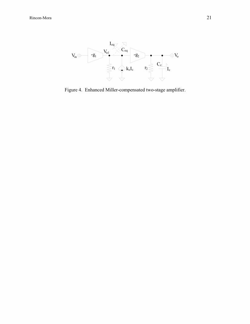
2.2 Multiplied-Miller Capacitor
Complementing the already existing voltage-mode gain factor with a current-mode
capacitor multiplier enhances the effects of the Miller capacitor. Figure 4 models such a circuit
configuration. The equivalent capacitance to ground that results at node n1 is not only multiplied

Rincon-Mora 7
by the Miller effect (A2 g2r2) but by the current-mode multiplier (kx). The difference between
this topology and that of a typical Miller configuration (Figure 1) is that capacitor Cc is no longer
connected to the output of the first stage directly. Instead, its current is sensed, multiplied by
current mirrors, and reapplied to node n1 via a current-controlled current source. As before, the
current flowing through Cc is
SCrgVSCAVSCVI c221nc21ncoc , (11)
thus CrgkSV
Ik
SV
IC c22x
1n
cx
1n
ceqeq ! (12)
Gain factor A2 refers to the gain across the second stage. The significance of this relation is that,
given a particular design, the size of Cc required to properly compensate the circuit is kx times
smaller using the proposed approach than using the standard Miller-compensation technique.
The resulting dominant pole and gain-bandwidth product are described by
Crgkr2
1P
c22x1
1n (13)
and Ck2
gGBW
cx
1 . (14)

Rincon-Mora 8
In the end, gain factor kx amplifies the effects of capacitor Cc. Furthermore, the RHP zero
present in typical Miller-compensated circuits is no longer existent in the proposed topology
because there is no feed-forward path around the inverting transconductor of the second stage.
III. Circuit Realization
A linear regulator is designed in a 1 µm biCMOS process to test the proposed technique.
The regulator is a two-stage amplifier with a class “A” output stage. Most regulators have a dc
open-loop gain of approximately 40 – 60 dB. Open-loop gain is limited to guarantee stability
due to the harshness of the loading conditions, load-current range is large and output capacitor is
high. Within a given application, the load current can vary from zero to anywhere above 100
mA. As a result, the output pole varies with load current (output impedance is a function of load
current). Furthermore, typical load capacitors range from 1 to 20 µF thereby pulling the output
pole to low frequencies.
The output stage of the regulator is a P-type common-source class “A” gain stage. This
choice results because the load only demands the IC to drive and not sink significant amounts of
current. Figure 5 shows the simplified version of the schematic using a folded-cascode
architecture as the first gain stage. Compensation is realized by combining the circuits shown in
Figures 3 and 4. Capacitor Cc is connected from the output to a diode-connected transistor,
mn22a. This transistor is used to bias the amplifier in steady-state conditions (when the
capacitor current is zero) and is also used to sense the displacement current flowing through
capacitor Cc. The ac current is thusly mirrored and injected back into high impedance node n_31
by means of transistors mn22b, mn22, mp22, and mp21. Node n_31 is the output of the first

Rincon-Mora 9
gain stage (equivalent to node n1 in Figure 4). Transistor mn32 is a natural NMOS transistor.
Its low threshold voltage (approximately 0 V) prevents mp22 from being crushed.
A buffer is used between the first and the second stage to drive the gate of the large
output PMOS device. A weak drive delays the response time during fast transient load-current
changes. The buffer, shown in detail in Figure 6, senses the load current by mirroring a fraction
of it through transistor mpox. This mirrored current is ultimately used to define the location of
the parasitic pole at the gate of power PMOS mpo. For high power efficiency and stability, its
location must be a function of the load. Like before, transistor mn31 is a natural NMOS device.
Its low threshold voltage allows the feedback circuit to effectively shut-off, when required, the
PMOS pass device. Bulk effects can be cancelled if a deep n+ trench diffusion and a buried n+
layer are available to isolate the natural device (isolate a p-epi region in which a natural device
can be built). The buffer and its benefits are described in [5]. Capacitor Cc2 along with readily
available components in the amplifier are used to realize the circuit of Figure 3. As a result,
node n_31 is further loaded with an equivalent capacitor equal to a multiplied version of Cc2.
This capacitor is used to compensate the high frequency feedback path through Cc, mn21b,
mn22, mp22, mp21, buffer, and mpo. This high frequency path has two main poles: one at the
output and one at node n_31. Capacitor Cc2 makes node n_31 dominant at high frequencies.
Careful layout is exercised to maximize the matching capabilities of mn21a, mn21b,
mn22a, mn22b, and their corresponding current sources. Input offset performance is sensitive to
these devices since they all determine how well the currents through transistors mn22a and
mn22b match. This characteristic is a disadvantage relative to standard Miller compensation
where only mn22b and mn21b, of the group mentioned earlier, need to match well, i.e., a
degradation of roughly 5 mV. Ultimately, more sources of input offset errors are significant in

Rincon-Mora 10
the circuit when the proposed technique is utilized. The current gain kx (chosen to be 10) is
defined by the mirror ratio between mn21a and mn21b (mn22a and mn22b) and is therefore
restricted by the physical constraints of the same. The tradeoff for matching is high gain; a large
spread between the matching devices yields high gain and, unfortunately, poor matching
characteristics and thus increased input offset voltages. On the positive side, the only additional
components required to compensate the circuit are Cc, Cc2, mn22a, and mn21a. Transistors
mn21a and mn22a are relatively small devices and capacitors Cc and Cc2 are already minimized
by the aforementioned technique.
Figure 7a shows the simulated open-loop response of the circuit without compensation,
with standard Miller compensation (Cc = 20 pF), and with enhanced-Miller compensation (Cc = 2
pF and kx = 10) under nominal conditions. As mentioned earlier, low loop gain is necessary in a
regulator circuit because of the variability of the load, i.e., load current ranges two orders of
magnitude, ESR may be zero or several Ohms, and the load capacitor can vary by 50 to 100 %
with temperature and process. The nominal load of the simulation shown in Figure 7a consisted
of a 0.1 µF capacitor to ground and a current sink of 10 mA. The ac response of the Miller and
enhanced-Miller compensated circuits are almost identical. In fact, the standard version, using a
Cc an order of magnitude larger, has less gain margin than the new version. This effect results
because, like in Figure 3, a high frequency LHP zero is introduced by Cc and the
transconductance of mn22a (1/gmn22a), which adds phase near the vicinity of the unity-gain
frequency. The circuit was stable up to a load capacitance of 21 µF and a load current of 220
mA over process and temperature. It was also stable with various values of Equivalent Series
Resistance (ESR) for the load capacitor (Figure 7b). Typical ESR’s can range up to several
Ohms. High frequency capacitors, on the other hand, can exhibit ESR’s of less than 0.5 [6].

Rincon-Mora 11
The phase-margin response of the circuit shown in Figure 7b (circuit under various harsh
loading conditions) is degraded from that of Figure 7a because large load capacitors pull the
output pole to lower frequencies and high load currents push the unity-gain frequency towards
higher frequencies close to the location of other parasitic poles. Load capacitors for linear
regulators normally range from 1 to 10 µF depending on the application and the particular
design. The cumulative effect of ESR and the bondwire resistance is a LHP zero. Stability, for
this design, is independent of ESR as is shown in Figure 7b. Without any ESR, the zero
introduced by the bondwire resistance is in the MHz region, i.e., 1 / 2 (60 m!) 1 µF ~ 2.6 MHz,
which helps keep phase margin but not significantly since it lies beyond the frequency range of
interest.
IV. Experimental Results and Discussion
Figures 8 and 9 show the experimental performance of the circuit under rapid load-
current changes. The load current is pulsed from zero to 200 mA and back down to zero with
rise and fall times of less than 100 ns. Any susceptibility towards instability would result in
oscillations under this test since the abrupt stimulus injects noise that spans a wide frequency
spectrum [7]. Figure 8 shows the transient response when no additional ESR is added in series
with the load capacitor (CL). The only ESR present is inherent to the capacitors and is below 0.1
!. Figure 9 shows the same type of response except that a 3 ! series resistor has been added as
intentional ESR. Figures 8 (a) and 9 (a) show the full period response while 8 (b) and 9 (b) only
show the negative transition, where oscillations are most prone to initiate. The total quiescent
current of the circuit is less than 30 µA during zero load-current conditions.

Rincon-Mora 12
The overshoot and the slow decay on the rising edge are a function of the load capacitor
and its ESR. High capacitance and low ESR prevents the node from overshooting significantly.
During the recovery from this positive overshoot, the output slews back down to its steady-state
value. This part of the response occurs because the output of the circuit is a class “A” output
stage with a small sink current determined by a resistive ladder (two 250 k resistors). The
falling edge, shown in Figures 8 (b) and 9 (b), has a different response because of the active pull-
up transistor in the output stage. During this transition, the regulator initially stays off thereby
allowing the full load to quickly discharge the output capacitor. Bandwidth and internal slew-
rate conditions at the gate of the large PMOS pass device determine how long the regulator takes
to start conducting current. Once it starts, the positive-feedback loop within the buffer helps
speed up the process until the negative-feedback gain is large enough to take control again.
Positive and negative overshoots occur during this period as a result.
It is evident that the regulator is stable with varying degrees of phase margin (depicted by
the settling time response) for a variety of load-capacitor values (up to 20 µF) with and without
additional ESR of up to 3 . The response was the same for several devices subjected to the
same tests. The circuit tends to be more stable with additional ESR. This results because ESR
effectively adds a Left-Hand Plane (LHP) zero at 1 / 2!RESRCL thereby adding phase between 1
and 60 kHz depending on the value of CL. The zero is also inclined to push the unity-gain
frequency towards higher frequencies thereby improving time response, in other words,
decreasing the time required for the circuit to react. Resistor RESR also increases the peak
overshoots because of the voltage drop created when capacitor CL charges and discharges.
Relatively low phase margin, rapid load pulses, and an internal positive feedback loop in the
buffer account for the large positive and negative overshoots of the signals in Figure 8.

Rincon-Mora 13
In conclusion, the circuit proved to be stable under a variety of loading conditions. Table
1 shows a summary of the performance parameters pertinent to the regulator. Load capacitor CL
needed to be at least 1.5 nF to prevent oscillations. Under the test setup utilized, the output
transiently goes below ground when CL is less than 1.5 nF. At this point, the load (an NPN
power transistor) is saturated thereby interacting with the circuit and causing oscillations during
recovery. The output is momentarily pulled to ground because capacitor CL is quickly
discharged by the load current during the time the IC takes to respond, while mpo is not sourcing
any current. Most relevant applications require output capacitors of more than 10 nF anyway.
V. Conclusion
A linear regulator, which is essentially a two-stage amplifier, is designed and fabricated
using a modified Miller-compensating scheme where an integrated capacitor is multiplied
“actively,” and in a controlled fashion, to compensate the circuit. A current-mode capacitor
multiplier is used to enhance the voltage-mode multiplying effects of Miller compensation. The
drawback, for the particular design in question, is deteriorated input offset voltage. This
disadvantage is alleviated with careful design and layout. Furthermore, in high frequency
applications, careful consideration must be given to the placement of the Left-Hand Plane (LHP)
introduced by the circuit: a low LHP zero degrades gain margin. This zero is manipulated by
controlling the transconductance of the diode-connected device, mn22a (adding more current
decreases the impedance thereby pushing the zero to higher frequencies). Additionally, during a
fast load transient event, the diode-connected device may turn-off temporarily thereby degrading
overall recovery time. Placing an additional current source (gates are passively de-coupled or
totally disconnected from the ones used by the technique) in parallel with mn21b and mn22b

Rincon-Mora 14
mitigates this negative effect. Although the technique has been applied to a folded-cascode
topology, the basic concept may be extended to other amplifier topologies. Simulations and
experimental results confirm the validity of the concept. The fabricated IC proves to be stable
for load currents of up to 200 mA, Equivalent Series Resistance (ESR) of up to 3 , and load
capacitors ranging from 1.5 nF to 21 µF. These results are achieved by using a significantly
lower compensating capacitor than would have been used had the teachings of standard Miller
compensation been adopted. The number of additional components required to compensate the
circuit is minimal and its overhead, in terms of silicon area, is negligible. Mitigating silicon area
requirements allows the circuit to be smaller thereby reducing overall cost. Furthermore, the
technique applies to the compensation of feedback circuits in general, Miller or otherwise.

Rincon-Mora 15
References
[1] A.S. Sedra and K.C. Smith, Microelectronic Circuits. New York: Holt,
Rinehart and Winston, Inc., 1987.
[2] P.R. Gray and R.G. Meyer, Analysis and Design of Analog Integrated Circuits.
New York: John Wiley & Sons, Inc., 1993.
[3] M. Ingels and M.S.J. Steyaert, “Design Strategies and Decoupling Techniques for
Reducing the Effects of electrical Interference in Mixed-Mode IC’s,” IEEE Journal of
Solid-State Circuits, Vol 32 # 7, pp. 1136-1141, July 1997.
[4] R. Cavin and W. Liu, Emerging Technologies, Designing Low Power Digital
Systems. Piscataway, NJ: Institute of Electrical and Electronics Engineers, 1996.
[5] G.A. Rincon-Mora and P.E. Allen, “A Low Voltage, Low Quiescent Current, Low
Drop-out Regulator,” IEEE Journal of Solid-State Circuits, Vol 33, pp. 36-44, January
1998.
[6] M. Kay, "Design and Analysis of an LDO Voltage Regulator with a PMOS Power
Device," Preliminary paper pending publication, Texas Instruments.
[7] B. C. Kuo, Automatic Control Systems. Englewood Cliffs, New Jersey: Prentice Hall,
1991.

Rincon-Mora 16
Table 1. Performance summary.
Measured Results
Line Regulation (Vsupply = 3 – 8 V) 2 mV/V
Load Regulation (ILoad = 0 – 200 mA) 0.275 mV/mA
CLoad 1.5 nF to 20 µF
ESR 3 !
Quiescent Current (ILoad = 0 A) 30 µA
Vsupply 1.25 to 8 V
Vinput-referred-offset (referred to Vbandgap) ±15 mV

Rincon-Mora 17
Figure Captions
Figure 1. Two-stage Miller-compensated amplifier.
Figure 2. Voltage-mode and current-mode capacitor multipliers.
Figure 3. Current-mode capacitor multiplier in a practical gain-stage circuit.
Figure 4. Enhanced Miller-compensated two-stage amplifier.
Figure 5. Simplified schematic of the linear regulator using the enhanced-Miller technique.
Figure 6. Detailed schematic of the regulator.
Figure 7a. Simulated Bode plot of the proposed circuit without compensation, with standard
Miller compensation, and with enhanced-Miller compensation under nominal conditions.
Figure 7b. Simulated Bode plot of the proposed circuit with enhanced-Miller compensation
under various loading conditions.
Figure 8. Experimental transient response of the fabricated regulator with zero ESR: (a) load
current is rapidly pulsed from zero to full range and back to zero and (b) load current is
pulsed from zero to full range only.
Figure 9. Experimental transient response of the fabricated regulator with 3 of ESR: (a) load
current is rapidly pulsed from zero to full range and back to zero and (b) load current is
pulsed from zero to full range only.
Figure 10. Die Plot.

Rincon-Mora 18
Vin Vo
Cc
CLr1 r2
-g1 -g2
Figure 1. Two-stage Miller-compensated amplifier.

Rincon-Mora 19
Vn1
V = -A Vo 2 n1
Cc
Ic
Vn1
CeqIcVo
C = (1 + A )Ceq 2 c
Vn1
CcIcIckx
Vn1
Ceq
IcI +ckxI =eq
Ieq
C = (1 + k )Ceq x c
(a) (b)
Figure 2. Voltage-mode and current-mode capacitor multipliers.

Rincon-Mora 20
Vn1
Ib
Vin
Vsupply
Cc
Vy
ymn1
kxymn2
mp1
Figure 3. Current-mode capacitor multiplier in a practical gain-stage circuit.
Rincon-Mora 21
Vin Vo
Ccr1 r2
-g1 -g2
Ickx
Vn1Ceq
Ieq
Ic
Figure 4. Enhanced Miller-compensated two-stage amplifier.

Rincon-Mora 22
Vbias
Cc2
Cc
Vo
Vsupply
Vreference
mn22a mn22bmn21b
mn21ax 10x
10xx
mn22mn21
mp21mp22
n_3
1
n_41mpo
mn32
Figure 5. Simplified schematic of the linear regulator using the enhanced-Miller technique.

Rincon-Mora 23
Cc2
Cc
Vo
Vsupply
mn22a mn22bmn21b
mn21ax 10x
10xx
mn22mn21
mp21mp22
n_3
1 n_41 mpo
Vreference
I bia
s
mpox41000/150/1
Buffer
mn31mn32
Figure 6. Detailed schematic of the regulator.

R
inco
n-M
ora
24
Fig
ure
7a.
S
imula
ted
Bo
de
plo
t o
f th
e p
rop
ose
d c
ircu
it w
ith
ou
t co
mpen
sati
on
, w
ith
sta
nd
ard
Mil
ler
com
pen
sati
on
, an
d w
ith
en
han
ced
-
Mil
ler
com
pen
sati
on
un
der
no
min
al c
on
dit
ion
s.

R
inco
n-M
ora
25
Fig
ure
7b
. S
imula
ted
Bo
de
plo
t o
f th
e pro
pose
d c
ircu
it w
ith e
nhan
ced-M
ille
r co
mpen
sati
on u
nder
var
ious
load
ing c
ondit
ions.

R
inco
n-M
ora
26
C =
1 u
FC
= 2
uF
C =
5.7
uF
C =
11 u
F C =
21 u
F
I
=
0 t
o 2
00 m
AL
oad
C =
1 u
F
C =
2 u
F
C =
5.7
uF
C =
11 u
F
C =
21 u
F
I
=
0 t
o 2
00 m
AL
oad
Add
ed E
SR
= 0
Add
ed E
SR
= 0
(a)
(b)
Fig
ure
8. E
xp
erim
enta
l tr
ansi
ent
resp
on
se o
f th
e fa
bri
cate
d r
egula
tor
wit
h z
ero E
SR
: (
a) l
oad
cu
rren
t is
rap
idly
pu
lsed
fro
m z
ero
to
full
ran
ge
and
bac
k t
o z
ero
an
d (
b)
load
cu
rren
t is
puls
ed f
rom
zer
o t
o f
ull
ran
ge
only
.

R
inco
n-M
ora
27
C =
1 u
F
C =
2 u
F
C =
5.7
, 11
, 21 u
FC
= 1
1 u
F
C =
21 u
F
I
=
0 t
o 2
00 m
AL
oad
Added
ES
R =
3 O
hm
s
C =
1 u
F
C =
2 u
F
C =
5.7
uF
I
=
0 t
o 2
00 m
AL
oad
Added
ES
R =
3 O
hm
s
(a)
(b)
Fig
ure
9. E
xp
erim
enta
l tr
ansi
ent
resp
on
se o
f th
e fa
bri
cate
d r
egu
lato
r w
ith
3
of
ES
R:
(a)
lo
ad c
urr
ent
is r
apid
ly p
uls
ed f
rom
zer
o t
o
full
ran
ge
and
bac
k t
o z
ero
an
d (
b)
load
cu
rren
t is
puls
ed f
rom
zer
o t
o f
ull
ran
ge
only
.

Rincon-Mora 28
Figure 10. Die Plot.