Accurate Quantitative Physics-of-Failure Approach to ...
24
Accurate Quantitative Physics-of-Failure Approach to Integrated Circuit Reliability Authors: Edward Wyrwas (DfR Solutions, LLC) Lloyd Condra (The Boeing Corporation) Avshalom Hava (Motorola)
Transcript of Accurate Quantitative Physics-of-Failure Approach to ...
Accurate Quantitative
Physics-of-Failure Approach to
Integrated Circuit Reliability
Authors: Edward Wyrwas (DfR Solutions, LLC)
Lloyd Condra (The Boeing Corporation)
Avshalom Hava (Motorola)
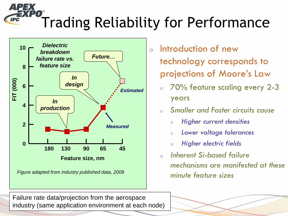
Trading Reliability for Performance
180 130 90 65 45 0
2
4
6
8
10
FIT
(0
00
)
Feature size, nm
Figure adapted from industry published data, 2008
In
production
Future…
In
design
Dielectric
breakdown
failure rate vs.
feature size
Estimated
Measured
o Introduction of new
technology corresponds to
projections of Moore’s Law
o 70% feature scaling every 2-3
years
o Smaller and Faster circuits cause
o Higher current densities
o Lower voltage tolerances
o Higher electric fields
o Inherent Si-based failure
mechanisms are manifested at these
minute feature sizes
Failure rate data/projection from the aerospace
industry (same application environment at each node)
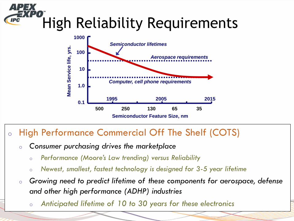
High Reliability Requirements
1995 2005 2015 0.1
1.0
10
100
1000
Me
an
Se
rvic
e lif
e,
yrs
.
Computer, cell phone requirements
Aerospace requirements
500 250 130 65 35
Semiconductor lifetimes
Semiconductor Feature Size, nm
o High Performance Commercial Off The Shelf (COTS)
o Consumer purchasing drives the marketplace
o Performance (Moore’s Law trending) versus Reliability
o Newest, smallest, fastest technology is designed for 3-5 year lifetime
o Growing need to predict lifetime of these components for aerospace, defense
and other high performance (ADHP) industries
o Anticipated lifetime of 10 to 30 years for these electronics
Modeling a Solution
• Create an easy to use software tool that can be used by multiple disciplines of engineers
– Accessible component data (datasheet limitations)
– Anticipated field conditions and component stresses
– With minimal access to manufacturer data
• Sometimes only censored data is available
• Back to the fundamentals
– Transistor theory and circuit analysis
– Physics-of-Failure (PoF) degradation models
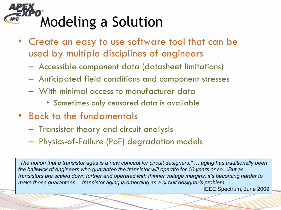
”The notion that a transistor ages is a new concept for circuit designers,” … aging has traditionally been
the bailiwick of engineers who guarantee the transistor will operate for 10 years or so…But as
transistors are scaled down further and operated with thinner voltage margins, it’s becoming harder to
make those guarantees… transistor aging is emerging as a circuit designer’s problem.
IEEE Spectrum, June 2009
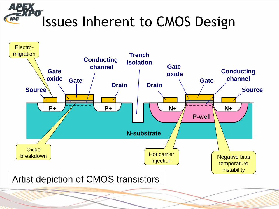
Issues Inherent to CMOS Design
Gate
oxide Gate
Source Drain
Conducting
channel Gate
oxide Gate
Drain Source
Conducting
channel
N-substrate
Trench
isolation
P+ P+
P-well
N+ N+
Electro-
migration
Oxide
breakdown Hot carrier
injection Negative bias
temperature
instability
Artist depiction of CMOS transistors
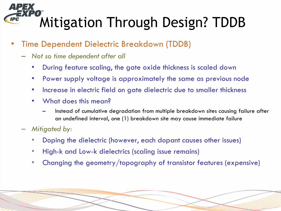
• Time Dependent Dielectric Breakdown (TDDB)
– Not so time dependent after all
• During feature scaling, the gate oxide thickness is scaled down
• Power supply voltage is approximately the same as previous node
• Increase in electric field on gate dielectric due to smaller thickness
• What does this mean?
– Instead of cumulative degradation from multiple breakdown sites causing failure after
an undefined interval, one (1) breakdown site may cause immediate failure
– Mitigated by:
• Doping the dielectric (however, each dopant causes other issues)
• High-k and Low-k dielectrics (scaling issue remains)
• Changing the geometry/topography of transistor features (expensive)
Mitigation Through Design? TDDB
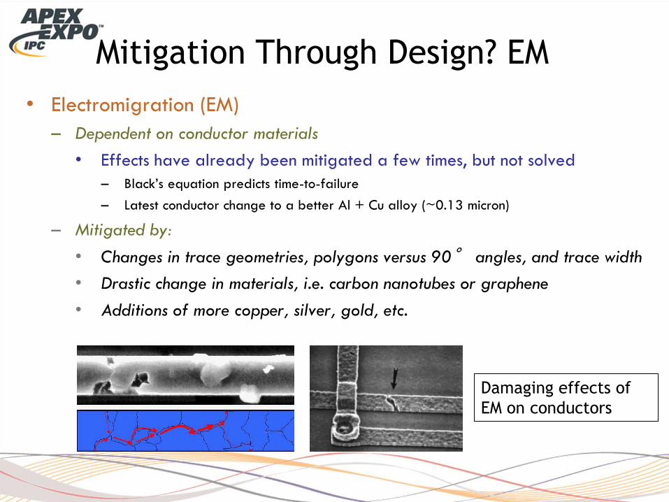
• Electromigration (EM)
– Dependent on conductor materials
• Effects have already been mitigated a few times, but not solved
– Black’s equation predicts time-to-failure
– Latest conductor change to a better Al + Cu alloy (~0.13 micron)
– Mitigated by:
• Changes in trace geometries, polygons versus 90° angles, and trace width
• Drastic change in materials, i.e. carbon nanotubes or graphene
• Additions of more copper, silver, gold, etc.
Mitigation Through Design? EM
Damaging effects of
EM on conductors
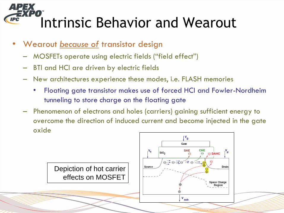
• Wearout because of transistor design
– MOSFETs operate using electric fields (“field effect”)
– BTI and HCI are driven by electric fields
– New architectures experience these modes, i.e. FLASH memories
• Floating gate transistor makes use of forced HCI and Fowler-Nordheim
tunneling to store charge on the floating gate
– Phenomenon of electrons and holes (carriers) gaining sufficient energy to
overcome the direction of induced current and become injected in the gate
oxide
Intrinsic Behavior and Wearout
Depiction of hot carrier
effects on MOSFET
• Hot Carrier Effects or Injection (HCI) Characteristics
– Caused by a single carrier gains sufficient kinetic energy, or
– Multiple carriers undergoing collisions that force them out of the directional path of electric field (the conducting channel)
– HCI has inverse Arrhenius relationship
• Activation energy -0.2 to -0.1 eV
• Lower temperatures ( ~35 to ~55°C) increase vulnerability
• Bias Temperature Instability
– Combined bias & temperature stresses are required for activation
• Fluctuations in temperature (overall device + self heating property)
• High temperatures cause molecular instability
• Requires lower electric fields than HCI
– Trap formation from electric fields are worse under negative bias (positive bias is ~90%+ recoverable)
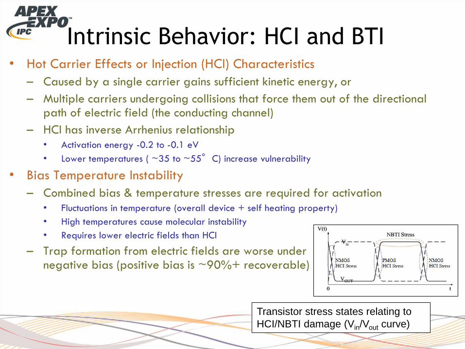
Intrinsic Behavior: HCI and BTI
Transistor stress states relating to
HCI/NBTI damage (Vin/Vout curve)
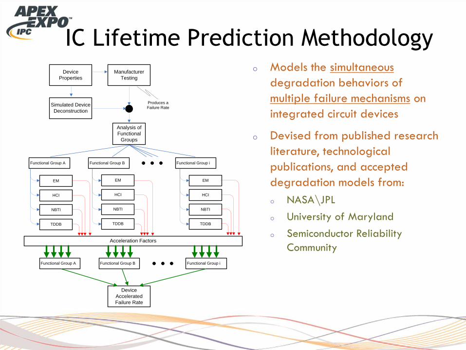
IC Lifetime Prediction Methodology
Produces a
Failure Rate
EM
HCI
NBTI
TDDB
EM
HCI
NBTI
TDDB
EM
HCI
NBTI
TDDB
Acceleration Factors
Analysis of
Functional
Groups
Functional Group A Functional Group B Functional Group i
Simulated Device
Deconstruction
Device
Properties
Manufacturer
Testing
Functional Group A Functional Group B Functional Group i
Device
Accelerated
Failure Rate
o Models the simultaneous
degradation behaviors of
multiple failure mechanisms on
integrated circuit devices
o Devised from published research
literature, technological
publications, and accepted
degradation models from:
o NASA\JPL
o University of Maryland
o Semiconductor Reliability
Community
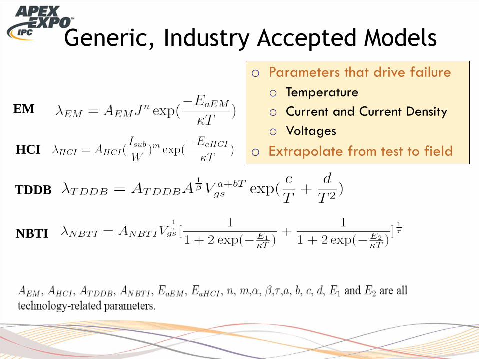
Generic, Industry Accepted Models
EM
HCI
TDDB
NBTI
o Parameters that drive failure
o Temperature
o Current and Current Density
o Voltages
o Extrapolate from test to field
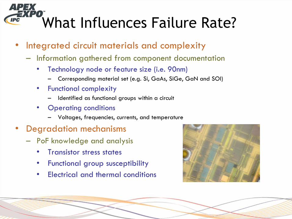
What Influences Failure Rate?
• Integrated circuit materials and complexity
– Information gathered from component documentation
• Technology node or feature size (i.e. 90nm)
– Corresponding material set (e.g. Si, GaAs, SiGe, GaN and SOI)
• Functional complexity
– Identified as functional groups within a circuit
• Operating conditions
– Voltages, frequencies, currents, and temperature
• Degradation mechanisms
– PoF knowledge and analysis
• Transistor stress states
• Functional group susceptibility
• Electrical and thermal conditions
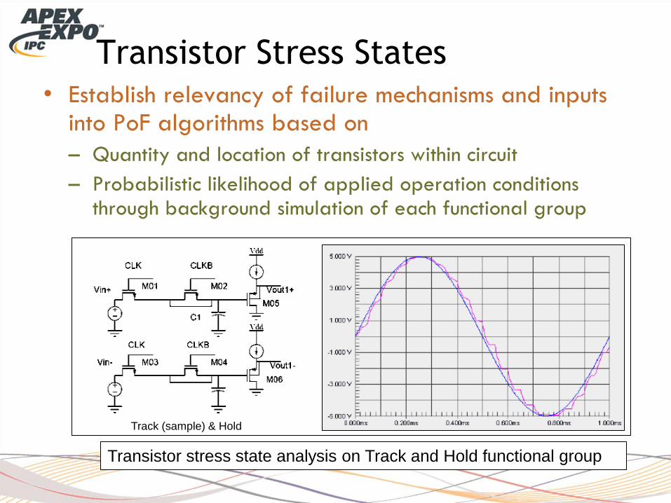
Transistor Stress States • Establish relevancy of failure mechanisms and inputs
into PoF algorithms based on
– Quantity and location of transistors within circuit
– Probabilistic likelihood of applied operation conditions through background simulation of each functional group
Track (sample) & Hold
Transistor stress state analysis on Track and Hold functional group
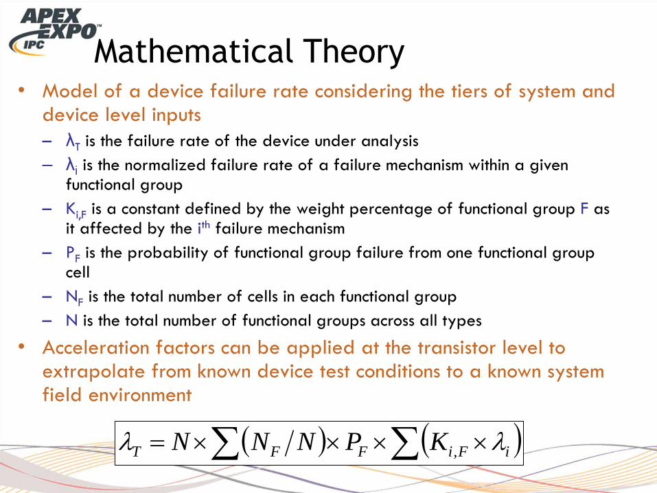
• Model of a device failure rate considering the tiers of system and device level inputs
– λT is the failure rate of the device under analysis
– λi is the normalized failure rate of a failure mechanism within a given functional group
– Ki,F is a constant defined by the weight percentage of functional group F as it affected by the ith failure mechanism
– PF is the probability of functional group failure from one functional group cell
– NF is the total number of cells in each functional group
– N is the total number of functional groups across all types
• Acceleration factors can be applied at the transistor level to extrapolate from known device test conditions to a known system field environment
Mathematical Theory
iFiFFT KPNNN ,
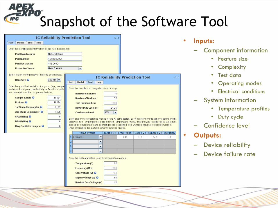
Snapshot of the Software Tool
• Inputs:
– Component information
• Feature size
• Complexity
• Test data
• Operating modes
• Electrical conditions
– System Information
• Temperature profiles
• Duty cycle
– Confidence level
• Outputs:
– Device reliability
– Device failure rate
Part Number Process
Technology
Field
Voltage
(V)
Test
Voltage
(V)
Field
Temperature
(°C)
Test
Temperature
(°C)
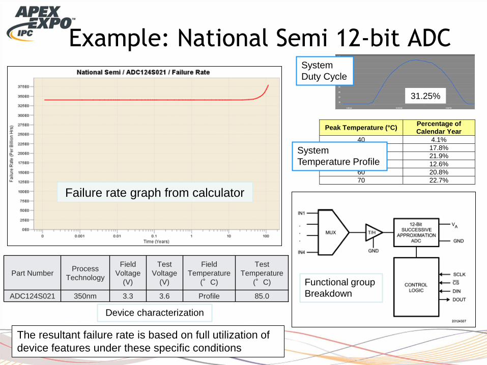
ADC124S021 350nm 3.3 3.6 Profile 85.0
Example: National Semi 12-bit ADC
Peak Temperature (°C) Percentage of Calendar Year
40 4.1%
45 17.8%
50 21.9%
55 12.6%
60 20.8%
70 22.7%
System
Duty Cycle
System
Temperature Profile
Functional group
Breakdown
Failure rate graph from calculator
Device characterization
31.25%
The resultant failure rate is based on full utilization of
device features under these specific conditions
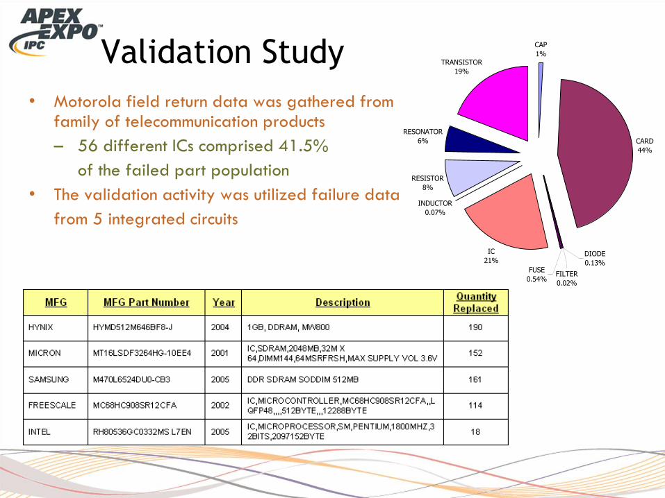
Validation Study
• Motorola field return data was gathered from a family of telecommunication products
– 56 different ICs comprised 41.5%
of the failed part population
• The validation activity was utilized failure data
from 5 integrated circuits
Electrical Failures Distribution
CAP
1%
CARD
44%
IC
21%
RESISTOR
8%
RESONATOR
6%
TRANSISTOR
19%
DIODE
0.13%
FILTER
0.02%
FUSE
0.54%
INDUCTOR
0.07%
0
2
4
6
8
10
12
14
16
18
20
Feb
-03
Dec
-03
Oct
-04
Au
g-0
5
Jun
-06
Ap
r-0
7
Feb
-08
Dec
-08
Mo
nth
ly F
aile
d I
Cs
0
100,000
200,000
300,000
400,000
500,000
600,000
700,000
Cu
mu
lati
ve
Wo
rkin
g M
on
ths
Cumulative Working Months
Monthly Failed ICs
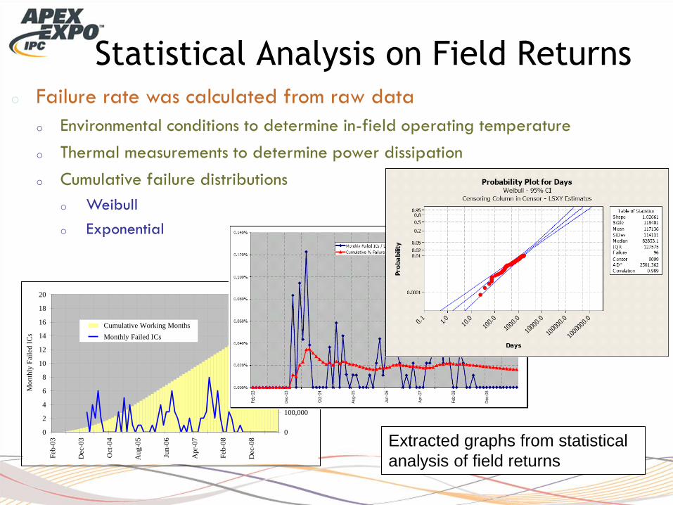
Statistical Analysis on Field Returns o Failure rate was calculated from raw data
o Environmental conditions to determine in-field operating temperature
o Thermal measurements to determine power dissipation
o Cumulative failure distributions
o Weibull
o Exponential
Extracted graphs from statistical
analysis of field returns
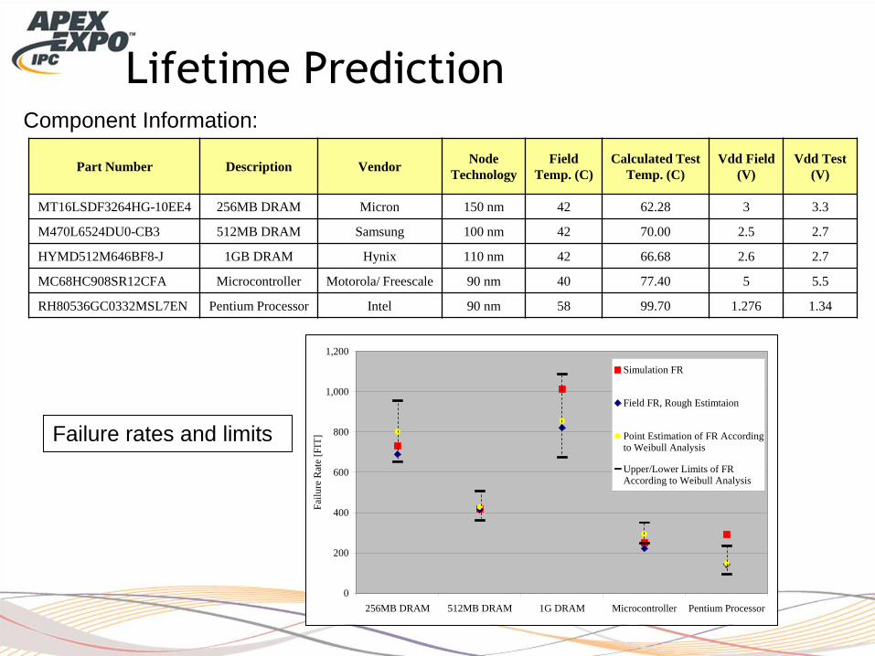
Lifetime Prediction
Part Number Description Vendor Node
Technology
Field
Temp. (C)
Calculated Test
Temp. (C)
Vdd Field
(V)
Vdd Test
(V)
MT16LSDF3264HG-10EE4 256MB DRAM Micron 150 nm 42 62.28 3 3.3
M470L6524DU0-CB3 512MB DRAM Samsung 100 nm 42 70.00 2.5 2.7
HYMD512M646BF8-J 1GB DRAM Hynix 110 nm 42 66.68 2.6 2.7
MC68HC908SR12CFA Microcontroller Motorola/ Freescale 90 nm 40 77.40 5 5.5
RH80536GC0332MSL7EN Pentium Processor Intel 90 nm 58 99.70 1.276 1.34
Component Information:
0
200
400
600
800
1,000
1,200
256MB DRAM 512MB DRAM 1G DRAM Microcontroller Pentium Processor
Fai
lure
Rat
e [F
IT]
Simulation FR
Field FR, Rough Estimtaion
Point Estimation of FR Accordingto Weibull Analysis
Upper/Lower Limits of FRAccording to Weibull Analysis
Failure rates and limits
Comparison of Results
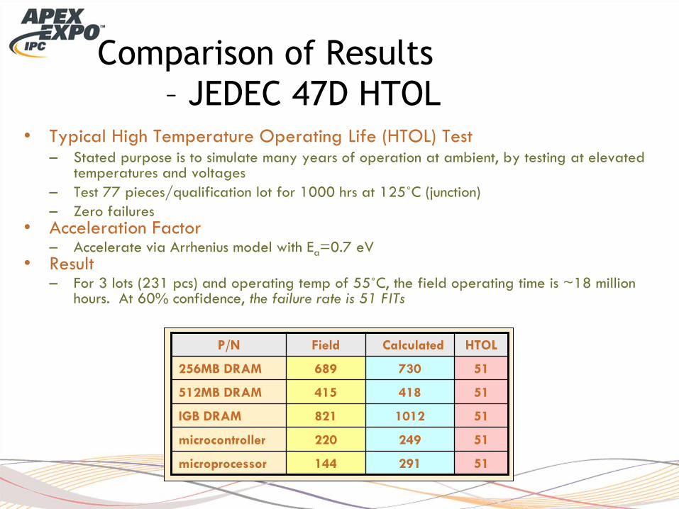
– JEDEC 47D HTOL • Typical High Temperature Operating Life (HTOL) Test
– Stated purpose is to simulate many years of operation at ambient, by testing at elevated temperatures and voltages
– Test 77 pieces/qualification lot for 1000 hrs at 125˚C (junction)
– Zero failures • Acceleration Factor
– Accelerate via Arrhenius model with Ea=0.7 eV • Result
– For 3 lots (231 pcs) and operating temp of 55˚C, the field operating time is ~18 million hours. At 60% confidence, the failure rate is 51 FITs
51 291 144 microprocessor
51 249 220 microcontroller
51 1012 821 IGB DRAM
51 418 415 512MB DRAM
51 730 689 256MB DRAM
HTOL Calculated Field P/N
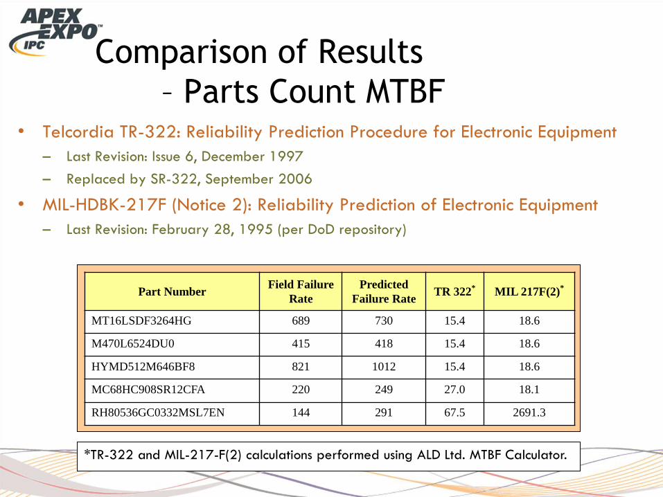
Comparison of Results
– Parts Count MTBF • Telcordia TR-322: Reliability Prediction Procedure for Electronic Equipment
– Last Revision: Issue 6, December 1997
– Replaced by SR-322, September 2006
• MIL-HDBK-217F (Notice 2): Reliability Prediction of Electronic Equipment
– Last Revision: February 28, 1995 (per DoD repository)
Part Number Field Failure
Rate
Predicted
Failure Rate TR 322* MIL 217F(2)*
MT16LSDF3264HG 689 730 15.4 18.6
M470L6524DU0 415 418 15.4 18.6
HYMD512M646BF8 821 1012 15.4 18.6
MC68HC908SR12CFA 220 249 27.0 18.1
RH80536GC0332MSL7EN 144 291 67.5 2691.3
*TR-322 and MIL-217-F(2) calculations performed using ALD Ltd. MTBF Calculator.
Application of Results
o Industry Standards
o VITA 51.2, Physics of Failure Reliability Predictions
o MIL-HDBK-217J, Reliability Prediction of Electronic Systems
o Addition of Physics-of-Failure requirements
o IEC TS 62239, Preparation of an Electronic Component Management Plan
o Addition of a wearout requirement
o Certification requirements
o ARP 4761
o ARP 5890
o Platform customer requirements
Where Can We Go From Here?
o Future roadmap of existing features:
o 65nm, 45nm, 32nm, 22nm technologies
o Additional functional groups
o Digital including logic and conditioners (e.g. gates)
o Analog for signal processing (e.g. opamps)
o Processor based (DSP, FPGA, etc)
o Customizable equivalent circuits and automated functional group
analysis for ASIC design
o “Expert mode”
o Modification of all default parameters
o Tradeoff analysis
o Performance vs. Reliability

Questions?
• Q & A
• Would you like additional information?
– Contact:
Edward Wyrwas
Member of Technical Staff
DfR Solutions, LLC
5110 Roanoke Place, Suite 101, College Park, MD 20740
(301) 474-0607 x304 <ph> (866) 247-9457 <fax> www.dfrsolutions.com