
Accurate Fault Modeling and Fault Simulation of Resistive ... · PDF fileAccurate Fault...
13
Accurate Fault Modeling and Fault Simulation of Resistive Bridges Vijay Sar-Dessai D. M. H. Walker Dept. of Electrical Engineering Dept. of Computer Science Texas A&M University Texas A&M University College Station, TX 77843 College Station, TX 77843 Ph: (409) 845-0531 Ph: (409) 862-4387 Fax: (409) 847-8578 e-mail: [email protected] e-mail: [email protected] Contact Author: D. M. H. Walker Dept. of Computer Science Texas A&M University College Station, TX 77843 Ph: (409) 862-4387 Fax: (409) 847-8578 e-mail: [email protected] Topic Areas: IC Testing Techniques Defect and Fault Tolerance Issues
Transcript of Accurate Fault Modeling and Fault Simulation of Resistive ... · PDF fileAccurate Fault...
Accurate Fault Modeling and Fault Simulation of Resistive Bridges
Vijay Sar-Dessai D. M. H. Walker
Dept. of Electrical Engineering Dept. of Computer ScienceTexas A&M University Texas A&M University
College Station, TX 77843 College Station, TX 77843Ph: (409) 845-0531 Ph: (409) 862-4387
Fax: (409) 847-8578e-mail: [email protected] e-mail: [email protected]
Contact Author: D. M. H. Walker
Dept. of Computer Science Texas A&M University College Station, TX 77843
Ph: (409) 862-4387 Fax: (409) 847-8578 e-mail: [email protected]
Topic Areas: IC Testing Techniques Defect and Fault Tolerance Issues
1
AbstractThis paper presents accurate fault models, an accuratefault simulation technique, and a new fault coveragemetric for resistive bridging faults in gate levelcombinational circuits at nominal and reduced powersupply voltages. We demonstrate that some faults haveunusual behavior, which has been observed in practice.On the ISCAS85 benchmark circuits we show that azero-ohm bridge fault model can be quite optimistic interms of coverage of voltage-testable bridging faults.
1 IntroductionWith the increasing density and complexity of VLSIchips, shorts between normally unconnected nodes areexpected to be the main type of manufacturing defect[1]. These shorts can be divided into two kinds: intra-gate shorts between nodes within a logic gate, andinter-gate (or external) shorts between outputs ofdifferent logic gates [2][3]. Inter-gate shorts, usuallycalled bridging faults, account for about 90% of allshorts [3][4]. Thus in order to accurately estimate thequality of a chip, it is important to have a faultsimulator that can simulate realistic bridging faults.
The accuracy of a bridging fault simulator dependson the following factors:• determination of the voltages at the nodes involved inthe bridge as functions of the bridge resistance andpower supply voltage• interpretation of the fault site voltage by gates fed bythe bridged nodes.
It is now well accepted that the traditional stuck-atfault model is inadequate for modeling bridging faults[5][6]. Most bridging fault simulators use otheralternatives for fault modeling, like the wired-AND,wired-OR, and voting models [7]. Much of the previouswork has either used analytical methods [3] todetermine the voltages at the bridged nodes and theirinterpretation by other gates downstream or has used atable-based approach [8] in which pre-computed tablesare used to insert voltages or logic values at the faultsite. The resistance of the bridge is usually assumed tobe 0Ω. However, as shown in [1], many bridges canhave significant resistance. Some resistive bridges areonly detected under certain sensitization andpropagation conditions. Some resistive bridges candegrade the voltage level and circuit timing withoutaffecting the logical function. In order to improve theaccuracy of the fault simulator, it is necessary toconsider the resistance of the bridge as well.
This paper presents an accurate bridging faultsimulation method that models the behavior of bridgingfaults by using pre-computed data from circuit
simulation at the fault site. Once this data has beeninserted at the fault site, gate-level logic simulation isdone everywhere else. This fault simulator is consideredto be accurate because this pre-computed data has beengenerated for almost all possible bridges involvingoutputs of pairs of gates in a combinational circuit. Itincludes some cases which were left unmodeled in [8].Considering resistive bridges instead of just zero-ohmbridges has also improved the accuracy of the faultsimulator.
It is well known that as the power supply voltage isdecreased, higher bridging resistances are detected[9][10][11]. This paper shows some cases in whichdecreasing the power supply voltage could cause a faultwhich is detected at a higher power supply voltage to beundetected at a lower power supply voltage. Althoughthis behavior has been predicted in [12] andexperimentally observed in [13], it has not been provenby specific examples. This work demonstrates suchcases with examples and discusses their impact onoverall fault coverage.
The remainder of this paper is organized as follows:Section 2 deals with the limitations of previous faultmodels, explains the fault model used in this bridgingfault simulator, and defines the fault coverage metricused in this work. Section 3 describes the constructionof look-up tables used in the fault simulator. Section 4describes the bridging fault simulation algorithm. Faultsimulation at decreased power supply voltage is dealtwith in Section 5. Section 6 presents some resultsobtained from benchmark circuits. Limitations of ourapproach are discussed in Section 7. Concludingremarks are made in Section 8.
2 Bridging Fault ModelsA bridging fault model should not only consider thebehavior of the gates involved in the bridge, but shouldinclude the driven gate behavior. This is because thelogical interpretation of the voltage at the bridged nodesdepends on the logical threshold of the gate to whichthe bridged node is connected. In reality, not only dodifferent gates have different thresholds, but each inputof a gate has a different threshold. This implies that twogates tied to the same bridged node can interpret thevoltage at the bridged node as different logical values,as shown in an example in [8]. This problem is called“The Byzantine General’s Problem” [14]. A bridgingfault model should also consider the resistance of thebridge, because it is unrealistic to assume that allbridges between gate outputs are pure shorts.
2
2.1 Previous fault modelsA number of bridging fault models have been proposedin previous work, like the wired-AND, wired-OR andvoting models. The wired model is inadequate to modelbridging faults because the voltages at the bridgednodes not only depend on the activated pull-up andpull-down networks and the transistor modelparameters, but also on the bridging resistance. Eventhough bridging faults in CMOS circuits almost alwaysresult in recognizable logic values [15][16][17], thewired model leads to an incorrect description of thebridging fault, as the example in [7] shows. In [7], avoting model has been proposed that uses a table-basedapproach for deciding the vote. The drawback of thisapproach is that it neglects the resistance of the bridge,and also ignores the “Byzantine General’s Problem”.The bridging fault simulator proposed by [8] is basedon accurate modeling of fault behavior, but it considerszero-ohm bridges only, and leaves some classes ofbridging faults unmodeled. In [18] the bridgingresistance was considered in the fault model, but thethreshold voltage of gates fed by the bridged nodes wasassumed to be VDD/2 for all gate inputs. A method ofsimulating bridging faults using variable gate logicthresholds has been proposed in [19]. A concept calledParametric Fault Model has been proposed in [3], inwhich the bridging resistance is taken into account, andinstead of propagating a faulty logic value to theprimary output, the detectable bridging resistanceinterval is propagated. However, this model is based ondetermining the detectable resistance by electricalequations rather than by circuit simulation and it didnot discuss some cases too.
2.2 Description of fault modelIn this paper, bridging faults have been modeled byHSPICE [20] circuit simulation of almost all possiblebridging fault configurations for all gates included inthe gate-level description of the ISCAS85 benchmarkcircuits. Each circuit was built using basic gates, and nocomplex gates were used. Each gate was implementedusing complementary CMOS logic. We used the SPICElevel 3 parameters for the HP CMOS14TB 0.5 µmprocess, running at a normal VDD of 3.3V. Thebenchmark circuits contain 22 different types of gates,and by exhaustively simulating different types ofbridging faults (explained below) that can occur invarious combinations of these gates, we obtain a set oflook-up tables containing data that is used at the faultsite during fault simulation.
In general, the following types of resistive bridgescan occur in a combinational circuit:
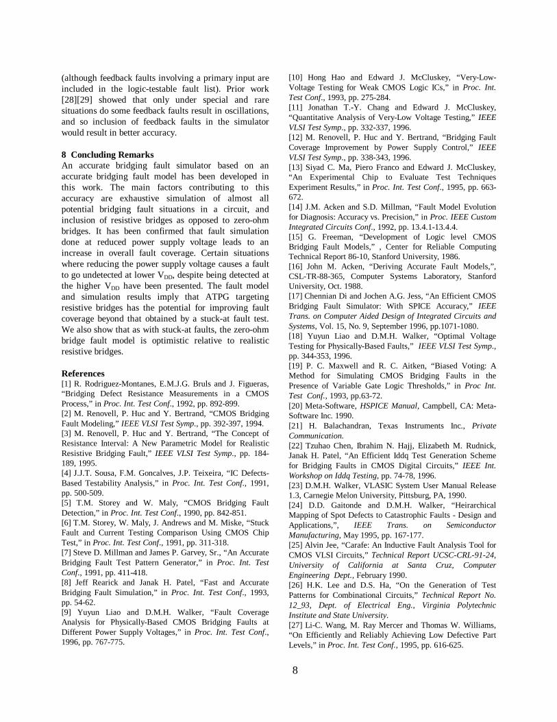
Case 1: Bridge between two primary inputs:We define a primary input as a circuit node that is
not at the output of any gate. This type of bridge is notdetectable by logic testing, because primary inputs are asource of infinite current, and any bridge between aprimary input carrying a logic 1 and another primaryinput carrying a logic 0 will not affect the functionalbehavior of the circuit. Hence this type of bridging faultis not modeled.
Case 2: Bridge between a primary input and any othernode:
Figure 1 shows a bridging fault between a primaryinput A and the output of a NAND2 gate, X. Node Xfeeds into 2 gates having different threshold voltages.The bridge resistance detectable at nodes P and Qdepends on the test vector at A, B, C as well as on thelogic threshold values of the 2 gates connected to nodeX.
For example, HSPICE simulation shows that if theapplied vector is A,B,C = 0,0,1, then we can detect abridging resistance up to 1600Ω at node P and up to1400Ω at node Q, assuming that other inputs of theAND2 and OR2 gates are held at their non-controllingvalues. The fault does not propagate along primaryinput A because of the reason stated earlier.
Case 3: Bridge between outputs of two gates (bridgednodes feeding into different gates):
Figure 2 illustrates a case in which the outputs of aNAND2 and a NOR2 gate are bridged, and the bridgednodes X and Y feed into different gates. The bridgeresistance detectable at the outputs of each of thesegates depends on the vector at A1, B1, A2, B2 as wellas on the logic thresholds of the gates connected tonodes X and Y.
Assuming that the vector at A1,B1,A2,B2 =1,0,1,1, HSPICE simulation of this case shows thatthe bridging fault will propagate along node X, and theresistance detectable is up to 1000Ω at P and up to1400Ω at Q. Due to the vector used and the thresholdsof the INV and the AND2 gate, the fault does notpropagate along node Y, and is undetectable at nodes Rand S.
Case 4: Bridge between outputs of two gates (bridgednodes feeding into same gate):
Figure 3 illustrates the case in which the outputs ofa NAND2 and NAND2 gate are bridged, and thebridged nodes feed into the same AND3 gate. Thebridge resistance detectable at node P depends only on
3
the vector at A1, B1, A2, B2 (assuming that the thirdinput of the AND3 gate is at its non-controlling value).
With a vector of A1,B1,A2,B2 = 1,0,1,1, HSPICEsimulation of this circuit shows that a bridge resistanceof up to 800Ω is detectable at node P.
Case 5: Bridge involving primary outputsIf two primary outputs are bridged to each other, the
case can be dealt with in a similar manner as in case 3,if we imagine the primary outputs to be nodes feedinggates having a logic threshold value of VDD/2, as wasdone in [18].
If a primary output is bridged to a primary input,this case would fall under case 2. If a primary output isbridged to a node that is neither a primary input nor aprimary output, this case would fall under case 3. Inboth situations we can imagine the primary output to bea node feeding a gate having a logic threshold value ofVDD/2.
The fault simulator we have built is based on thisaccurate fault model. By doing HSPICE simulations ofall possible gate combinations in all the above cases, wecan accurately model the behavior of bridging faults,and insert the data obtained from the simulations intothe fault simulator at the fault site.
2.3 Fault coverage metricSince metal bridging resistance mainly falls in therange from 0Ω to 1000Ω [1], a geometric distributionused in [18] is found to be a good fit. The PDF of thebridging resistance is:
P(Rb) =1− (1− p)Rb (1)
where Rb is the bridging resistance and p = 0.00258
for the data in [1].The normalized fault coverage c(i) for the bridging
fault configuration i can be computed using:
c(i) =1− (1− p)Rb ( i)
1− (1− p)Rb max( i) (2)
where Rb(i ) is the detectable resistance for the
bridging fault configuration i, and Rbmax(i ) is the
maximum detectable resistance at the fault site for thebridging fault configuration i.
The fault coverage of a test vector v is given by:
∑=
=N
ivv ic
NC
1
)(1
(3)
where )(icv is the normalized fault coverage for the
bridging fault i using that test vector v and N is thetotal number of logic-testable faults in the circuit(assuming equally likely faults).
The cumulative fault coverage of a test vector set isgiven by:
∑=
=N
ihc ic
NC
1
)(1
(4)
where )(ich is the highest achieved normalized fault
coverage for the bridging fault i .
Since )(ich is normalized, cC is the coverage of
all bridging faults potentially detectable by low-speedvoltage test, which we refer to as logic-testablebridging faults.
3 Construction of Look-up TablesIn order to obtain information about the behavior of thecircuit at the fault site for fault simulation, we havebuilt a number of look-up tables. Prior to theconstruction of the look-up tables, the logic threshold ofeach type of gate in the ISCAS85 circuits wasdetermined (we assumed that for a given gate, all inputshave the same logic threshold). There are three types oflook-up tables, one for each type of bridging faultclassified under case 2, case 3, and case 4 explained inthe previous section.
Case 2: For this type of bridge involving a primaryinput and any other node, construction of the table wasdone by simulating a bridge between a DC source andthe output of a gate. For all test vectors that excite thisfault, the maximum detectable resistance wasdetermined by comparing the voltage at the output ofthe gate with the logic thresholds Vth of all gates.Figure 4 (a) illustrates this principle for the circuit inFigure 1. As the resistance of the bridge increases, thevoltage at node X approaches its fault-free value. Thecrossover point between this voltage and the logicthreshold of the gate connected to node X determinesthe maximum detectable resistance. The high gain ofthe logic gates ensures that before and after thiscrossover point, the voltages at P and Q are restored totheir faulty and good logic values respectively. Thetable contains the following information at each entry:(a) vector at primary input and inputs of the gate(b) logic threshold of gate connected to bridged node(c) maximum detectable resistance under conditions (a)
and (b)We have built one table for each type of gate in the
ISCAS85 circuit. Since there are only 22 different typesof gates, we have 22 different tables.
Case 3: For this type of bridge involving outputs of twogates, construction of the table was done by simulating
4
a bridge between the outputs of two gates for allpossible vectors that excite the fault. Referring to Figure2, for each vector the maximum detectable resistancewas determined by comparing the voltage at nodes Xand Y with logic thresholds of all gates. As shown inFigure 4(b), as the bridge resistance is increased, thevoltages at X and Y approach their fault-free values.The crossover point between the voltage at nodes X andY and the logic threshold values determine themaximum detectable resistance. Each table entrycontains the following information:(a) vector at bridged gate inputs(b) fault propagation path (along bridged nodes)(c) logic threshold of gate connected to propagation
path(d) maximum detectable resistance under conditions
(a), (b) and (c)If we are to build one table per bridged pair of gates,
with the 22 different types of gates in the ISCAS85circuits there could be a total of 253 such tables, if weconsider all combinations. However, as pointed out in[17], we can analyze which bridges are the most likelyand generate tables only for them. Tables for otherbridges which rarely occur could be built during a pre-analysis for each circuit. The approach we haveimplemented is to generate tables for all combinationsof pairs of gates having a fan-in of 5 or less. This isbecause of the fact that bridges involving outputs ofgates with a larger fan-in (NAND8, AND8, NOR8,AND9 in the ISCAS85 circuits) occur extremely rarely(as shown in Table 2, under “Large-case BFs”) amongstthe target bridges in our implementation of thebenchmark circuits, and are left unmodeled. Thus wehave generated 171 tables for case 3.
Case 4: For this type of bridge involving bridgedoutputs of two gates feeding into the same gate,construction of the tables was done by simulating abridge between the outputs of two gates, with theoutputs feeding a third gate. The circuit was simulatedfor all possible vectors that excite the fault, and thevoltage at the output of this third gate was monitored.The bridging resistance at which the voltage at thisnode changed from its faulty value to its fault-free valuewas determined to be the maximum detectable bridgingresistance. Each entry in the table contains thefollowing information:(a) vector at inputs of gates whose outputs are bridged(b) maximum detectable resistance under condition (a).
We need to generate one table for each combinationof 3 gates. Since this number is extremely large, theapproach we have used is to model only those cases that
occur in the ISCAS85 circuits. Again, if the bridgesinvolve outputs of gates having a fan-in larger than 5,these cases are not modeled. Another type of bridgingfault falling under this case is that shown in Figure 5.This type of bridge has been found to be extremely rareamongst the target bridges in the ISCAS85 circuits (asshown in Table 2, under the column “Other droppedBFs”), and is left unmodeled. Thus we have generated20 tables case 4.Some case 4 bridging faults exhibit anomalous behaviorin terms of the maximum detectable resistance. Anexample is circuit in Figure 6 (a), which showed thebehavior depicted in Figure 6 (b) when simulated at lowvoltage (2V) with a vector A1,B1,A2,B2 = 0,0,0,1.Instead of the detectable resistance being in the intervalof 0Ω to the maximum detectable resistance Rbmax, itlies in the interval [Rbmin, Rbmax]. A similar caseinvolving an XOR2 gate with a low-resistance bridgeinserted between its inputs was confirmed in an actualcircuit [21]. During the table construction of such cases,the entry in the table corresponding to the maximumdetectable resistance is replaced with a resistanceinterval. (In all other cases, it is implicitly assumed thatthe lower limit of detectable resistance is 0Ω).
The tables for cases 2 to 4 occupy about 3MB ofspace, and table construction time was considerable,due to the many HSPICE simulations that had to beperformed. One way to reduce the construction timewould be to use the property of input equivalence in thepull-up and pull-down networks in any gate. Forinstance, in the case of a bridge involving a NAND2gate, simulation with inputs 1,0 and 0,1 would bethe same if the pull-up transistors are of the same size.
All entries in each table have been arranged indecreasing order of maximum detectable resistance, sothat in the future we can use them for ATPG.
During each HSPICE simulation, the resistance wasswept from 0 to 3000Ω. Thus even if the actualmaximum detectable resistance exceeded 3000Ω, thetable entry showed 3000Ω. We chose this value becauseusing equation (1), we noted that at 3000Ω thedetection probability was 99.95%, which was highenough to assume detection of any detectable resistivebridge, as shown by the data in [1].
4 Bridging Fault SimulatorImplementing the bridging fault simulator involvedobtaining the fault list and implementing the faultsimulation algorithm.
5
4.1 Fault list preparationEven though we are considering external bridges only,the list of faults to be considered for logic testing ofbridging faults could still be large (of the order ofn2
where n is the number of nodes in the circuit) ifwe were to consider all possible external bridges. Hencea reduced fault set is obtained by randomly choosingbridging faults from the all-pair bridging fault list. Thenumber of bridging faults in this reduced fault list isdetermined from the reduction ratio (extractedfaults/all-pair faults) listed in [22]. Alternatively, adefect simulator [23][24][25] can be used to generate arealistic bridging fault list.
From the reduced fault list, bridging faults betweenprimary inputs are eliminated, because they cannot betested by logic testing.
Feedback faults are discarded from the fault list.Although feedback bridging faults can potentially betested by logic testing, some of them may causeoscillations, which makes it difficult to model suchfaults. We will return to a discussion on feedbackbridges in a later section.
From the list of logic-testable bridging faults,bridging faults which are not modeled are dropped.Faults which fall under this class have been explainedin Section 3. As shown in Table 2, very few such faultsoccur.
Bridging faults eliminated in the above steps form alist of faults that can be detected by IDDQ testing. InIDDQ testing, a bridging fault is detected if the nodesinvolved in the bridge are set to opposite logic values,and the bridging resistance is low enough to cause adetectable IDDQ increase.
4.2 Fault simulation algorithmThe fault simulation procedure is carried out in thefollowing manner:• For each fault in the set of logic-testable faults, wedetermine the maximum detectable resistance from thelook-up table associated with that bridge. Thismaximum detectable bridging resistance depends onlyon the gates whose output nodes are bridged and thegates fed by the bridged nodes, and is independent ofthe applied test vector. This resistance gives anindication of the best fault coverage we can achieve forthis fault.• For each vector in the test set, the fault-free logicvalue at each node is determined. A list of excited faultsis formed from the logic-testable fault list.• For each excited fault, the look-up table is used todetermine the bridging resistance detectable at the faultsite. We follow the convention used in [3] to simulate
the faulty circuit. In this convention, the resistanceinterval, which specifies the range of resistances thatcan be detected by that test vector, is placed at the faultsite. For example, for the case of a primary inputbridged to any other node (Figure 1), the interval[0,1600] is inserted at node P (if the non-bridged inputof the AND2 gate is at logic 1) and the interval[0,1400] is inserted at node Q (if the non-bridged inputof the OR2 gate is at logic 0).• Fault simulation continues from the fault site towardsthe primary output with the propagation of theresistance interval at each node. During this forwardsimulation, the resistance interval can get reduced iftwo or more nodes carrying resistance intervals feedinto the same gate. The resistance interval at the outputof such gate can be a union or an intersection of theintervals at the inputs of the gate. This implies that thedetectable resistance interval can either remain thesame or decrease from its value at the fault site, andmay lead to a loss of fault coverage at the primaryoutput.• Once the resistance intervals at the primary outputsare known, the normalized fault coverage c(i) for eachfault excited by this vector is computed using equation(2). If c(i) is equal to 100%, then we have detected themaximum possible bridging resistance, and this faultcan be dropped from the logic-testable fault list. Thus, afault is dropped only if the bridging resistance intervaldetectable at the primary outputs is the maximumdetectable bridging resistance interval at the fault site.We could use a more relaxed criteria for dropping, thatis, we could drop a fault if the normalized coverage iswithin ∆ of 100%, in which case more faults will bedropped per test vector.
• We then compute the fault coverage vC of this test
vector using equation (3).• The above procedure is repeated for each vector. Foreach fault, we keep track of the best fault coverageobtained so far. This figure is then used to compute the
cumulative fault coverage cC of the entire test vector
set using equation (4).If the PDF of the bridging resistance is not known,
then we can decide whether to drop a fault or not byexamining the detectable resistance intervals. In thiscase, a higher detectable resistance implies better faultcoverage, assuming that higher resistance bridges areless probable.
6
5 Fault Simulation at Decreased Power Supply VoltageIt is well known that decreasing the power supplyvoltage VDD results in a larger bridging resistance beingdetected [9][10][11][12]. Thus we can obtain anincreased overall bridging fault coverage by decreasingVDD. In [12], the authors discussed some cases in whichdecreasing VDD reduces the detectable resistance. Thefirst case was called a “favorable” case from the point ofview of fault coverage improvement, because it resultedin an increase in maximum detectable resistance withdecreased VDD. The second case was called “partiallyfavorable” because the maximum detectable resistancefirst increased and then decreased with decreasing VDD.This indicates that this bridging fault was detectable athigher VDD and undetectable at certain lower VDD
values. The implication of this is that fault coveragemay not necessarily increase with decreased VDD.However, the authors claimed that since these cases area “mathematical possibility but never appeared in usualdesign”, the favorable cases are predominant, thusleading to increased overall fault coverage.
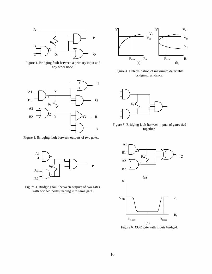
We have discovered some cases of bridging faultsin common circuit configurations in which the fault isdetectable at a higher VDD value but undetectable atdecreased VDD values. These cases fall under case 4 asdiscussed in Section 2, in which outputs of two gatesare bridged, with the bridged nodes feeding into thesame gate. Figure 7 shows such a case, involving aNAND2 gate having bridged inputs.
Table 1 shows the result of HSPICE simulation ofthis circuit for different test vectors that excite thisfault, along with the maximum detectable resistanceRbmax at node Z for two different values of VDD. (An Xin the table means that the fault is undetectable).
The results of this simulation indicate that atdecreased VDD, the bridging fault is undetectable forsome test vectors, even though it is detectable at ahigher value of VDD. Some test vectors can detect ahigher bridging resistance. In [13], it was shown thatsome circuits escaped fault detection at low voltageeven though the faults were detected at higher VDD.
However, since bridging faults that fall under thiscase occur relatively few times in the ISCAS85 circuits,the impact of this behavior on overall fault coverage isnegligible, as shown in the next section. Even ifsituations like these do exist in a circuit, the overallfault coverage still improves with decreased VDD, as theresults in the following section demonstrate.
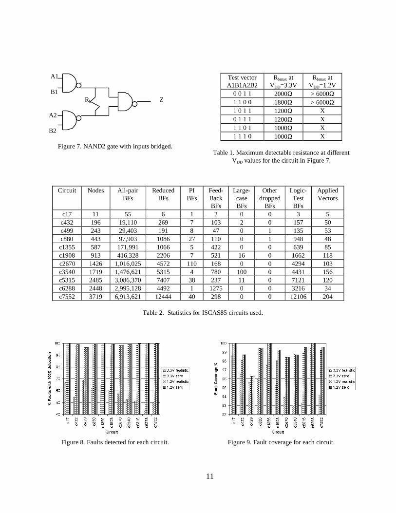
6 Results and DiscussionThe bridging fault simulator was run on the ISCAS85benchmark circuits. Table 2 gives some statistics ofthese benchmark circuits. For each circuit, the tablelists the total number of external nodes, the number ofall-pair bridging faults, randomly selected (reduced)bridging faults, faults between two primary inputs,feedback bridging faults, faults between outputs oflarge fan-in gates, bridging faults not modeled becauseof their special nature, bridging faults which can bepotentially detected by voltage testing (which forms thelogic-testable fault list), and the number of applied testvectors.
The test vectors were obtained from an automatictest pattern generator for stuck-at faults [26]. This alsogave us an indication of how good a fault coverage wecan obtain for resistive bridging faults using a stuck-attest set.
Each circuit was simulated at VDD=3.3V, 2.4V and1.2V, and for different resistance distributions. Theresults of some of the simulations are displayed inFigure 8 and Figure 9.
Figure 8 shows the percentage of faults completelydetected (dropped) by the test vector set, withsimulation done at VDD=3.3V and VDD=1.2V, and foran average resistance distribution using equation (1)(realistic bridges) and a zero-ohm resistancedistribution (zero-ohm bridges). Figure 9 shows thefault coverage for the entire test vector set.
In the case of zero-ohm bridges, a fault isconsidered detected with a 100% fault coverage and isdropped if any resistance interval associated with thatfault propagates to a primary output. Thus the faultcoverage in this case is the same as the percentage offaults detected. This is similar to the fault droppingcriteria used in stuck-at fault simulators. In the case ofrealistic bridges, if there is a loss of fault coverage asthe fault propagates to the primary outputs, the fault isnot dropped and the normalized fault coverage will notbe 100%.
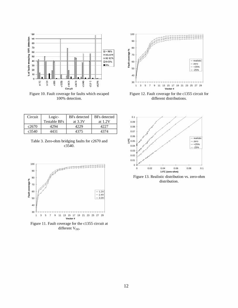
The following observations can be made withreference to Figure 8 and Figure 9:• At 3.3V, even though the percentage of realisticbridges completely detected (those for which the faultcoverage is equal to the maximum possible faultcoverage) is low (Figure 8), the fault coverage (Figure9) is high. This is because for the faults which escapedcomplete detection, the maximum resistance detectedwas high, though not equal to the maximum detectableresistance. Figure 10 shows the distribution of faultcoverage for faults which escaped 100% detection. Formost circuits, more than half of these faults had a fault
7
coverage exceeding 90%. The figure also shows thatvery few faults had a 0% fault coverage.• For zero-ohm bridges, the percentage of detectedfaults is equal to the fault coverage, since every faultthat contributes to the overall fault coverage has a100% fault coverage.• At 3.3V and 1.2V, the percentage of zero-ohmbridges completely detected (Figure 8) and their faultcoverage (Figure 9) was higher than the correspondingnumbers for realistic bridges. This is due to the fact thatfor zero-ohm bridges, the fault is dropped and the faultcoverage is 100% for any resistance interval at theprimary output.• For realistic bridges, the percentage of completelydetected bridges at 1.2V is more than the correspondingnumber at 3.3V (Figure 8). This is also the case forfault coverage of realistic bridges (Figure 9). Thisconfirms previous results that fault coverage improveswith decreasing VDD, and also suggests that even ifthere are a few isolated faults in which the fault isundetectable at lower VDD but detectable at higher VDD,the overall fault coverage still improves with decreasedVDD due to the relatively fewer number of such faults.• However, for zero-ohm bridges, there are 2 circuits(c2670 and c3540) for which the fault coverage at 1.2Vis lower than the fault coverage at 3.3V (Table 3 andFigure 9). This is because the fault coverage is high at3.3V due to the large number of detected faults, and at1.2V those few faults which escape detection cause theoverall fault coverage to drop. This anomaly occursonly for these two circuits because these circuits have arelatively higher number of case 4 bridges than theother circuits, and as explained in section 5, case 4bridges are responsible for decreased fault coverage atlower VDD.• At 1.2V, the maximum detectable resistance at thefault site as well as the detectable resistance at theprimary outputs was very high (> 3000Ω) in mostbridging faults. However, since in our HSPICEsimulations we placed a limit of 3000Ω for theresistance sweep, almost all faults were completelydetected. This explains the very high percentages forthe data at 1.2V in Figure 8. This tends to make thedata slightly optimistic. If there was a much higherlimit in our resistance sweep, then, for example, themaximum detectable resistance at the fault site couldhave been 10KΩ, and we could have detected up to6KΩ at the primary output. The fault would not havebeen dropped in this case, but it is dropped in ourapproach.
Figure 11 shows how the fault coverage improves asthe fault simulation progresses (for the first 30 vectors)
for the c1355 circuit at 3 different values of VDD,assuming realistic bridges. It is clear that the faultcoverage increases as VDD decreases. However, Figure10 also shows that the coverage for the first 10-15vectors is lower at 1.2V than at 2.4V and 3.3V. Thereason for this is that our coverage metric is relative.The resistance interval detected rises with decreasingvoltage, but the maximum detectable resistance riseseven faster, and occurs for fewer sensitization andpropagation conditions. Thus the probability ofobtaining the best coverage is lower for each vector.
Figure 12 shows how the fault coverage improves asthe fault simulation progresses (for the first 30 vectors),for the c1355 circuit at VDD=3.3V, with 4 differentbridging resistance distributions. The ± 25% cases arefor a ± 25% change in the mean value of the realresistance distribution. As expected, lower resistivebridges have higher coverage. The curves also showthat a vector that is good for one resistance distributionis also good for other distributions.
However, as shown in Figure 13, the coverage ofrealistic resistive bridges remains lower than that ofzero-ohm bridges even as the coverage of zero-ohmbridges goes to 100%. This result is similar to what hasbeen found comparing zero-ohm bridges to stuck-atfaults [27].
7 LimitationsLike other bridging fault simulators built on a table-based method, our fault simulator has certainlimitations. The first is that we have to create a largenumber of look-up tables prior to running the faultsimulator. The number of look-up tables depends on thetype of gates used in the circuits, and increases with thenumber of different types of gates. In addition, with achange in device parameters, a new set of look-uptables has to be created. If the fault simulator is to berun at several different power supply voltages, again anew set of look-up tables has to be created for eachvalue of VDD.
The second limitation is that although almost allbridging fault situations have been dealt with during thecreation of the look-up tables, there are a few whicheither cannot be modeled or are computationallyexpensive to model. These cases have been explained inSection 3. Although we have determined that thesecases occur relatively rarely in our implementation ofbenchmark circuits, inclusion of these cases duringfault simulation can result in an improvement inaccuracy.
A third limitation of our simulator is that feedbackbridging faults are not considered for logic testing,
8
(although feedback faults involving a primary input areincluded in the logic-testable fault list). Prior work[28][29] showed that only under special and raresituations do some feedback faults result in oscillations,and so inclusion of feedback faults in the simulatorwould result in better accuracy.
8 Concluding RemarksAn accurate bridging fault simulator based on anaccurate bridging fault model has been developed inthis work. The main factors contributing to thisaccuracy are exhaustive simulation of almost allpotential bridging fault situations in a circuit, andinclusion of resistive bridges as opposed to zero-ohmbridges. It has been confirmed that fault simulationdone at reduced power supply voltage leads to anincrease in overall fault coverage. Certain situationswhere reducing the power supply voltage causes a faultto go undetected at lower VDD, despite being detected atthe higher VDD have been presented. The fault modeland simulation results imply that ATPG targetingresistive bridges has the potential for improving faultcoverage beyond that obtained by a stuck-at fault test.We also show that as with stuck-at faults, the zero-ohmbridge fault model is optimistic relative to realisticresistive bridges.
References [1] R. Rodriguez-Montanes, E.M.J.G. Bruls and J. Figueras,“Bridging Defect Resistance Measurements in a CMOSProcess,” in Proc. Int. Test Conf., 1992, pp. 892-899.[2] M. Renovell, P. Huc and Y. Bertrand, “CMOS BridgingFault Modeling,” IEEE VLSI Test Symp., pp. 392-397, 1994.[3] M. Renovell, P. Huc and Y. Bertrand, “The Concept ofResistance Interval: A New Parametric Model for RealisticResistive Bridging Fault,” IEEE VLSI Test Symp., pp. 184-189, 1995.[4] J.J.T. Sousa, F.M. Goncalves, J.P. Teixeira, “IC Defects-Based Testability Analysis,” in Proc. Int. Test Conf., 1991,pp. 500-509.[5] T.M. Storey and W. Maly, “CMOS Bridging FaultDetection,” in Proc. Int. Test Conf., 1990, pp. 842-851.[6] T.M. Storey, W. Maly, J. Andrews and M. Miske, “StuckFault and Current Testing Comparison Using CMOS ChipTest,” in Proc. Int. Test Conf., 1991, pp. 311-318.[7] Steve D. Millman and James P. Garvey, Sr., “An AccurateBridging Fault Test Pattern Generator,” in Proc. Int. TestConf., 1991, pp. 411-418.[8] Jeff Rearick and Janak H. Patel, “Fast and AccurateBridging Fault Simulation,” in Proc. Int. Test Conf., 1993,pp. 54-62.[9] Yuyun Liao and D.M.H. Walker, “Fault CoverageAnalysis for Physically-Based CMOS Bridging Faults atDifferent Power Supply Voltages,” in Proc. Int. Test Conf.,1996, pp. 767-775.
[10] Hong Hao and Edward J. McCluskey, “Very-Low-Voltage Testing for Weak CMOS Logic ICs,” in Proc. Int.Test Conf., 1993, pp. 275-284.[11] Jonathan T.-Y. Chang and Edward J. McCluskey,“Quantitative Analysis of Very-Low Voltage Testing,” IEEEVLSI Test Symp., pp. 332-337, 1996.[12] M. Renovell, P. Huc and Y. Bertrand, “Bridging FaultCoverage Improvement by Power Supply Control,” IEEEVLSI Test Symp., pp. 338-343, 1996.[13] Siyad C. Ma, Piero Franco and Edward J. McCluskey,“An Experimental Chip to Evaluate Test TechniquesExperiment Results,” in Proc. Int. Test Conf., 1995, pp. 663-672.[14] J.M. Acken and S.D. Millman, “Fault Model Evolutionfor Diagnosis: Accuracy vs. Precision,” in Proc. IEEE CustomIntegrated Circuits Conf., 1992, pp. 13.4.1-13.4.4.[15] G. Freeman, “Development of Logic level CMOSBridging Fault Models,” , Center for Reliable ComputingTechnical Report 86-10, Stanford University, 1986.[16] John M. Acken, “Deriving Accurate Fault Models,”,CSL-TR-88-365, Computer Systems Laboratory, StanfordUniversity, Oct. 1988.[17] Chennian Di and Jochen A.G. Jess, “An Efficient CMOSBridging Fault Simulator: With SPICE Accuracy,” IEEETrans. on Computer Aided Design of Integrated Circuits andSystems, Vol. 15, No. 9, September 1996, pp.1071-1080.[18] Yuyun Liao and D.M.H. Walker, “Optimal VoltageTesting for Physically-Based Faults,” IEEE VLSI Test Symp.,pp. 344-353, 1996.[19] P. C. Maxwell and R. C. Aitken, “Biased Voting: AMethod for Simulating CMOS Bridging Faults in thePresence of Variable Gate Logic Thresholds,” in Proc Int.Test Conf., 1993, pp.63-72.[20] Meta-Software, HSPICE Manual, Campbell, CA: Meta-Software Inc. 1990.[21] H. Balachandran, Texas Instruments Inc., PrivateCommunication.[22] Tzuhao Chen, Ibrahim N. Hajj, Elizabeth M. Rudnick,Janak H. Patel, “An Efficient Iddq Test Generation Schemefor Bridging Faults in CMOS Digital Circuits,” IEEE Int.Workshop on Iddq Testing, pp. 74-78, 1996.[23] D.M.H. Walker, VLASIC System User Manual Release1.3, Carnegie Melon University, Pittsburg, PA, 1990.[24] D.D. Gaitonde and D.M.H. Walker, “HeirarchicalMapping of Spot Defects to Catastrophic Faults - Design andApplications,”, IEEE Trans. on SemiconductorManufacturing, May 1995, pp. 167-177.[25] Alvin Jee, “Carafe: An Inductive Fault Analysis Tool forCMOS VLSI Circuits,” Technical Report UCSC-CRL-91-24,University of California at Santa Cruz, ComputerEngineering Dept., February 1990.[26] H.K. Lee and D.S. Ha, “On the Generation of TestPatterns for Combinational Circuits,” Technical Report No.12_93, Dept. of Electrical Eng., Virginia PolytechnicInstitute and State University.[27] Li-C. Wang, M. Ray Mercer and Thomas W. Williams,“On Efficiently and Reliably Achieving Low Defective PartLevels,” in Proc. Int. Test Conf., 1995, pp. 616-625.

9
[28] Y.-J. Kwon and D.M.H. Walker, “Yield Learning viaFunctional Test Data,” in Proc. Int. Test Conf., 1995, pp.626-635.[29] Haluk Konuk and F. Joel Ferguson, “Oscillation andSequential Behavior Caused by Interconnect Opens in DigitalCMOS Circuits,” in Proc. Int. Test Conf., 1997, pp. 597-606.
10
A
P Rb B
C X Q
Figure 1. Bridging fault between a primary input andany other node.
P
A1 X
B1 Q Rb A2
B2 Y R
S
Figure 2. Bridging fault between outputs of two gates.
A1 B1
Rb P A2
B2
Figure 3. Bridging fault between outputs of two gates,with bridged nodes feeding into same gate.
V V Vx
Vx
Vth Vth
Vy
Rmax Rb Rmax Rb (a) (b)
Figure 4. Determination of maximum detectablebridging resistance.
Rb
Figure 5. Bridging fault between inputs of gates tiedtogether.
A1
B1 Rb Z A2
B2
(a) V
VDD Vz
Rb
Rbmin Rbmax
(b)Figure 6. XOR gate with inputs bridged.
11
A1
B1 Rb Z
A2
B2
Figure 7. NAND2 gate with inputs bridged.
Test vectorA1B1A2B2
Rbmax atVDD=3.3V
Rbmax atVDD=1.2V
0 0 1 1 2000Ω > 6000Ω1 1 0 0 1800Ω > 6000Ω1 0 1 1 1200Ω X0 1 1 1 1200Ω X1 1 0 1 1000Ω X1 1 1 0 1000Ω X
Table 1. Maximum detectable resistance at differentVDD values for the circuit in Figure 7.
Circuit Nodes All-pairBFs
ReducedBFs
PIBFs
Feed-BackBFs
Large-caseBFs
Otherdropped
BFs
Logic-TestBFs
AppliedVectors
c17 11 55 6 1 2 0 0 3 5c432 196 19,110 269 7 103 2 0 157 50c499 243 29,403 191 8 47 0 1 135 53c880 443 97,903 1086 27 110 0 1 948 48c1355 587 171,991 1066 5 422 0 0 639 85c1908 913 416,328 2206 7 521 16 0 1662 118
c2670 1426 1,016,025 4572 110 168 0 0 4294 103c3540 1719 1,476,621 5315 4 780 100 0 4431 156c5315 2485 3,086,370 7407 38 237 11 0 7121 120c6288 2448 2,995,128 4492 1 1275 0 0 3216 34c7552 3719 6,913,621 12444 40 298 0 0 12106 204
Table 2. Statistics for ISCAS85 circuits used.
Figure 8. Faults detected for each circuit. Figure 9. Fault coverage for each circuit.
12
Figure 10. Fault coverage for faults which escaped100% detection.
Circuit Logic-Testable BFs
BFs detectedat 3.3V
BFs detectedat 1.2V
c2670 4294 4229 4227c3540 4431 4375 4374
Table 3. Zero-ohm bridging faults for c2670 andc3540.
30
40
50
60
70
80
90
100
1 3 5 7 9 11 13 15 17 19 21 23 25 27 29Vector #
Fau
lt co
vera
ge %
1.2V2.4V3.3V
Figure 11. Fault coverage for the c1355 circuit atdifferent VDD.
30
40
50
60
70
80
90
100
1 3 5 7 9 11 13 15 17 19 21 23 25 27 29Vector #
Fau
lt co
vera
ge %
realisticzero+25%-25%
Figure 12. Fault coverage for the c1355 circuit fordifferent distributions.
0
0.01
0.02
0.03
0.04
0.05
0.06
0.07
0.08
0.09
0.1
0 0.02 0.04 0.06 0.08 0.11-FC (zero-ohm)
1-F
C realisticzero+25%-25%
Figure 13. Realistic distribution vs. zero-ohmdistribution.


![Accurate Fault Modeling and Fault Simulation of Resistive ...faculty.cs.tamu.edu/walker/pubs/sardessai98.pdf · The bridging fault simulator proposed by [8] is based on accurate modeling](https://static.fdocuments.net/doc/165x107/5f57d134e454a8594468c8f4/accurate-fault-modeling-and-fault-simulation-of-resistive-the-bridging-fault.jpg)


