
Accuracy Limitations in Specular- Mode Optical Topography...
28
Fred L. Terry, Jr., SPIE Metrology, Inspection, and Process Control for Microlithography XVII Accuracy Limitations in Specular- Mode Optical Topography Extraction Fred L. Terry, Jr. Dept of EECS / University of Michigan 734-763-9764 734-763-9324 (fax) [email protected] http://www.eecs.umich.edu/~fredty
Transcript of Accuracy Limitations in Specular- Mode Optical Topography...

Fred L. Terry, Jr., SPIE Metrology, Inspection, and Process Control for Microlithography XVII
Accuracy Limitations in Specular-Mode Optical Topography
Extraction
Fred L. Terry, Jr.
Dept of EECS / University of Michigan734-763-9764
734-763-9324 (fax)[email protected]
http://www.eecs.umich.edu/~fredty

Fred L. Terry, Jr., SPIE Metrology, Inspection, and Process Control for Microlithography XVII
Outline
• Goal: Use Specular Reflected Light Measurements from Gratings (Scatterometry) for Control of CD/Topography
• UofM Group: 1st Demos of Real-Time Monitoring and Endpoint Control of Photoresist CD in Etch Chambers
– Ex Situ & In Situ Results– Demos on O2 Plasma Trim-back of Photoresist for Gate– Requires Adaptation to Measurement Accuracy
Limitations• Simulations and Implications for Future of
Scatterometry as Process Control Sensor

Fred L. Terry, Jr., SPIE Metrology, Inspection, and Process Control for Microlithography XVII
Spectroscopic Ellipsometry
•
• Tan(Ψ) And Cos(∆) Are Measured by Ellipsometry—Functions of wavelength and incident angle
)cos()2sin( ),2cos(
)exp()tan(//
∆⋅Ψ=Ψ=
∆⋅Ψ===
βα
ρ iEEEE
RR
isrs
iprp
s
p
Substrate
Thin Film Stack
Eip
Eis
Erp
Ers
Light Source
Polarizer Analyzer
Monochromator&
Detector
Sample with Grating

Fred L. Terry, Jr., SPIE Metrology, Inspection, and Process Control for Microlithography XVII
Grating ⇔ Anisotropic Thin Film Analogy
Λ
ε1(λ)
ε2(λ) ε2(λ) ε2(λ)
ε1(λ) ε1(λ) ε1(λ)
W
D
Substrate
Thin Film Stack
( )ε λ
Substrate
Thin Film Stack
D εx
εz
εy
• Line Height ⇔ Film Thickness
• Line Shape ⇔ Optical Dielectric Function
Anisotropic Thin Film1-D Photonic Crystal

Fred L. Terry, Jr., SPIE Metrology, Inspection, and Process Control for Microlithography XVII
Specular Spectroscopic Scatterometry• Probes Wavelength Dependence of Scattering from a
Given Line Size/Shape• Grating Amplifies & Averages Single Line Effects• Grating Periodicity Aids Accurate Diffraction Solution• Result Sub-Wavelength Topography Sensitivity• Extremely High Sensitivity to Line Height (D) ⇒
Analogous to Thin Film Thickness• Very Good Sensitivity to Linewidth (W) & Line-shape
Under Proper Circumstances ⇒ Analogous to Parameterized Extraction of Optical Dielectric Function of Thin Film
• Accuracy of Topography Extraction Analogous to Accuracy of ε(λ) Extraction From Thin Films Using SE
– Will Fail If Grating Is Too Shallow (Effective Optical Thickness Fails to Produce Thin Film Interference Effect)
Fred L. Terry, Jr., SPIE Metrology, Inspection, and Process Control for Microlithography XVII
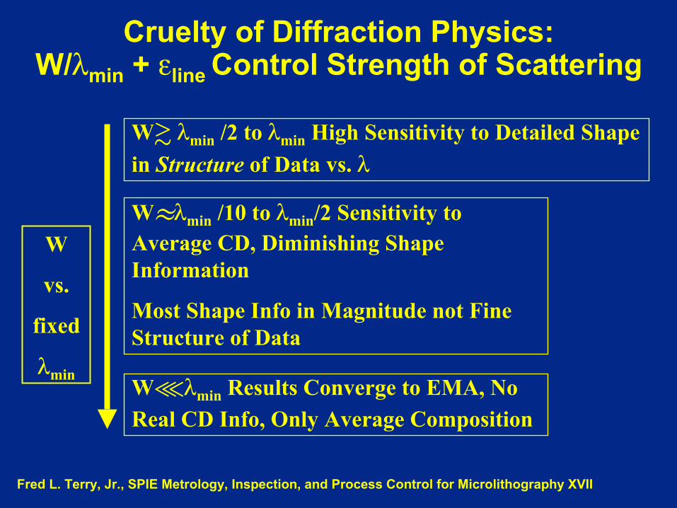
Cruelty of Diffraction Physics:W/λmin + εline Control Strength of Scattering
W
vs.
fixed
λmin
W λmin /2 to λmin High Sensitivity to Detailed Shape in Structure of Data vs. λ
W≈λmin /10 to λmin/2 Sensitivity to Average CD, Diminishing Shape Information
Most Shape Info in Magnitude not Fine Structure of Data
W λmin Results Converge to EMA, No Real CD Info, Only Average Composition

Fred L. Terry, Jr., SPIE Metrology, Inspection, and Process Control for Microlithography XVII
Topography Extraction Example W>λmin
• Experimental Data Taken at 7° AOI with Sopra GESP-5 Ellipsometer
• 350 nm Line/ 700 nm Period Photoresist on 31.7nm SiO2 on Si
• Successively Improved Topography Estimations Using Levenberg-Marquardt Non-Linear Regression
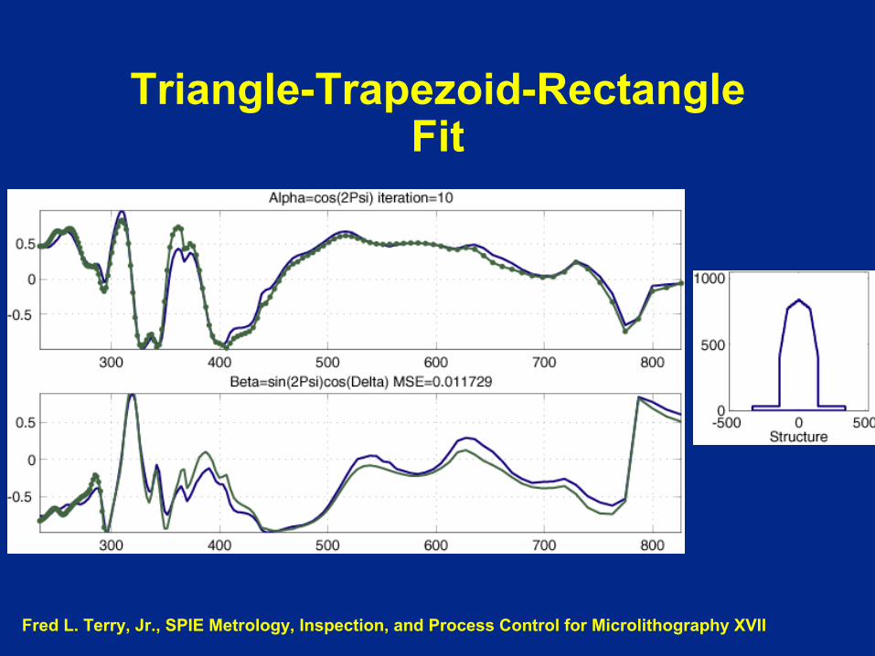
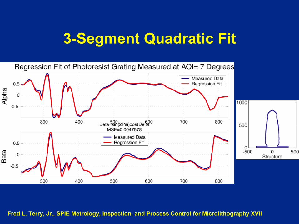
– Trapezoid (3 parameters)– Trapezoid on Rectangular Base (4 parameters)– Triangular Top on Trapezoid on Rectangle (5 parameters)– 3 Quadratic Segments with Zero Top Width (Triangle-
Trapezoid-Trapezoid with Curvature, 9 parameters)

Fred L. Terry, Jr., SPIE Metrology, Inspection, and Process Control for Microlithography XVII
Submicron Grating• ~0.35µm Line/Space
Grating In Photoresist/300Å SiO2/Si
• Accurate Photoresist N(λ) Obtained by SE Measurement of Similarly Prepared Unpatterned Film
• Period Measured as 0.700 µm Using 1st Order Diffraction Angle at Multiple λ’s

Fred L. Terry, Jr., SPIE Metrology, Inspection, and Process Control for Microlithography XVII
Trapezoidal Fit 400-825 nm

Fred L. Terry, Jr., SPIE Metrology, Inspection, and Process Control for Microlithography XVII
Trapezoidal Fit

Fred L. Terry, Jr., SPIE Metrology, Inspection, and Process Control for Microlithography XVII
Trapezoid on Rectangle Fit
Fred L. Terry, Jr., SPIE Metrology, Inspection, and Process Control for Microlithography XVII
Triangle-Trapezoid-Rectangle Fit
Fred L. Terry, Jr., SPIE Metrology, Inspection, and Process Control for Microlithography XVII
3-Segment Quadratic Fit

Fred L. Terry, Jr., SPIE Metrology, Inspection, and Process Control for Microlithography XVII
Extracted Topography Comparison

Fred L. Terry, Jr., SPIE Metrology, Inspection, and Process Control for Microlithography XVII
3-Level Quadratic Fit Parameters, Confidence
Limits, & Cross-
Correlation Coefficients
Term Value 95.4% conf. Limit Units
h1 146.51 4.55 nm m11 0.7389 0.0097 slope m12 -0.4698 0.011 quadratic curvature
h2 545.72 36.05 nm m21 0.3461 0.0272 slope m22 -0.1921 0.0282 quadratic curvature
h3 112.35 34.79 nm m31 0.0803 0.0529 slope m32 -0.1933 0.0659 quadratic curvature
h1 m11 m12 h2 m21 m22 h3 m31 m32 h1 1 0.356-0.217-0.369-0.176 0.121 0.267 0.101 0.04m11 0.356 1 -0.88 -0.34 -0.31 0.354 0.301-0.098 0.219m12-0.217 -0.88 1 0.373 -0.02 -0.08-0.363-0.146-0.009h2 -0.369 -0.34 0.373 1 0.512 -0.527-0.993-0.369-0.108m21-0.176 -0.31 -0.02 0.512 1 -0.981-0.493 0.286-0.474m22 0.121 0.354 -0.08-0.527-0.981 1 0.517 -0.31 0.501h3 0.267 0.301-0.363-0.993-0.493 0.517 1 0.394 0.082m31 0.101-0.098-0.146-0.369 0.286 -0.31 0.394 1-0.866m32 0.04 0.219-0.009-0.108-0.474 0.501 0.082-0.866 1
Fit Was Pushed to the Limits of Data

Fred L. Terry, Jr., SPIE Metrology, Inspection, and Process Control for Microlithography XVII
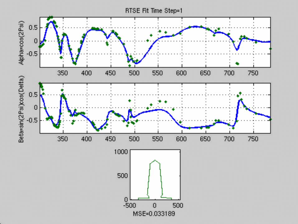
RTSE Etch Movie• In Situ Sopra Real-Time
Spectroscopic Ellipsometry Monitoring of Photoresist Trim-Back in Lam 9400 TCP
• Data Collect at 63.5° AOI• Non-Linear Filter Method to
Detect Endpoint• This Experiment Stopped at
200nm• Work of Drs. Hsu-Ting Huang,
Ji-Woong Lee, Pramod Khargonekar, and Fred Terry

Fred L. Terry, Jr., SPIE Metrology, Inspection, and Process Control for Microlithography XVII
sprt7_tritraprect.mov
Trim to Target CD Movie

Fred L. Terry, Jr., SPIE Metrology, Inspection, and Process Control for Microlithography XVII
In Situ Optical CD/Automated Etch to Target CD
• O2 Plasma Photoresist Trim in Lam 9400 TCP
• In Situ Real-Time Spectroscopic Ellipsometry Monitoring of Photoresist Grating Structure
• Off-Line RCWA Analysis of Grating Diffraction Problem
• Nonlinear Filtering Algorithm for Real-Time Data Analysis
– Completely Hands-off Automated Etch to Target CD
• Before Etching (top):– Bottom CD: 296 nm– Feature Height: 777 nm
• After Trim-back (bottom):– Bottom CD: 200 nm (target)– Feature Height: 697 nm

Fred L. Terry, Jr., SPIE Metrology, Inspection, and Process Control for Microlithography XVII
RTSE Etch Monitoring: Over-Fitting
• Attempt to Fit for Under-Cut of Resist• Over-Parameterization Due to Limited
Absolute Accuracy of Measurement• In This Case, Accuracy is Limited by Stray
Light, Lower UV Photon Counts– Usable Minimum Wavelength ~300nm– Some Distortion of Peak/Valley Shapes
Fred L. Terry, Jr., SPIE Metrology, Inspection, and Process Control for Microlithography XVII

Fred L. Terry, Jr., SPIE Metrology, Inspection, and Process Control for Microlithography XVII

Fred L. Terry, Jr., SPIE Metrology, Inspection, and Process Control for Microlithography XVII
Simulations of ITRS Photoresist Milestones
• Simulated Data using Model DUV Photoresist at 2010, 2013, and 2016 Technology Nodes
• Rectangular Profiles Assumed with:– Λ=90nm W=25±1.5nm Thick=100nm– Λ=64nm W=18 ± 1.1nm Thick=80nm– Λ=44nm W=13 ± 0.7nm Thick=50nm
• Assumed 190-800nm Spectroscopic Ellipsometry Measurements
• Good News: Diminishing but Usable CD Sensitivity to 2016
• Bad News: Loss of Detailed Shape Sensitivity even at 2010

Fred L. Terry, Jr., SPIE Metrology, Inspection, and Process Control for Microlithography XVII
Simulated ~40nm PR Line Λ=90nm
200 300 400 500 600 700 800-1
-0.5
0
0.5
1Alpha
wavelength (nm)
Alp
ha
200 300 400 500 600 700 800-1
-0.5
0
0.5
1Beta
wavelength (nm)
Bet
a
-60 -40 -20 0 20 40 600
20
40
60
80
100
120
nm
nm
Can Detailed Shape Information Be Extracted?

Fred L. Terry, Jr., SPIE Metrology, Inspection, and Process Control for Microlithography XVII
Fit Using Rectangular Only Model
200 300 400 500 600 700 800-1
-0.5
0
0.5
1Alpha
wavelength (nm)
Alp
ha
200 300 400 500 600 700 800-5
0
5
wavelength (nm)
Cha
nge
in A
lpha
x 1
00
200 300 400 500 600 700 800-1
-0.5
0
0.5
1Beta
wavelength (nm)
Bet
a
200 300 400 500 600 700 800-4
-2
0
2
wavelength (nm)
Cha
nge
in B
eta
x 10
0
-60 -40 -20 0 20 40 600
20
40
60
80
100
120 • Rectangle Fit Averages More Complex Structure
• Examine Structure Differences in Data Through Derivatives vs. λ

Fred L. Terry, Jr., SPIE Metrology, Inspection, and Process Control for Microlithography XVII
d3β/dλ3 For Complex Line & Rectangular Fit
200 300 400 500 600 700 800-8
-6
-4
-2
0
2
4
6x 10⁻⁴
nm
d3 β/dλ3
-60 -40 -20 0 20 40 600
20
40
60
80
100
120
No Structural Difference in Data Vs. Fit, All Information Concerning the More Complex Shape is in the Small Absolute Differences

Fred L. Terry, Jr., SPIE Metrology, Inspection, and Process Control for Microlithography XVII
Structure of Data and Fit
• Fitting with a Rectangle-Only Geometry Yields NO Structure Differences, Only Magnitude Differences
• Examining Derivatives of Data and Fit Illustrates Complete Lack of Structural Differences
• VERY High Instrument Accuracy Needed For Detailed Topography Extraction Without Resorting to VUV Measurements
• High Accuracy RCWA Calculations Required for Simulation/Regression

Fred L. Terry, Jr., SPIE Metrology, Inspection, and Process Control for Microlithography XVII
Conclusions• Extraction of Topography Using Specular-Mode
Spectroscopic Ellipsometry and Related Techniques Provides Outstanding Height and Average CD Capabilities to the End of the ITRS
• Detailed Lineshape Extraction Ability Exists But Gets Worse As W/λmin Decreases
• Situation Better for Gate Materials vs. Photoresist (ε)• Possibly Achievable but Very High Accuracy
Measurements Are Required for Detailed Shape Extraction
– Instrumentation, Alignment, and Simulation Accuracy Must All be Very Good
• VUV & EUV Scatterometry Needed for the Future• Unanswered Questions on Line-Edge Roughness, Line
Material Variations, etc.

Fred L. Terry, Jr., SPIE Metrology, Inspection, and Process Control for Microlithography XVII
Acknowledgements
• Initial Work Funded by SRC Center of Excellence for Automated Semiconductor Manufacturing
– Project Ended August, 1999• Research funded in part by: AFOSR/DARPA MURI
Center for Intelligent Electronics Manufacturing (AFOSR F49620-95-1-0524)
– Projected Ended August, 2001• Research funded in part by: NIST Intelligent Control of
the Semiconductor Patterning Process (70NANB8H4067)
– Project Ended June, 2002• Industry Support Badly Needed for Continued
University Efforts in this Area