Acceptors in GaAs: Experiment and Theory
45
Chair seminar, 03.07.2013 Shallow Acceptors in GaAs: Experiment and Theory G. Münnich , A. Donarini , M. Wenderoth, and J. Repp
Transcript of Acceptors in GaAs: Experiment and Theory

Chair seminar, 03.07.2013
Shallow Acceptors in GaAs: Experiment and Theory
G. Münnich, A. Donarini, M. Wenderoth, and J. Repp

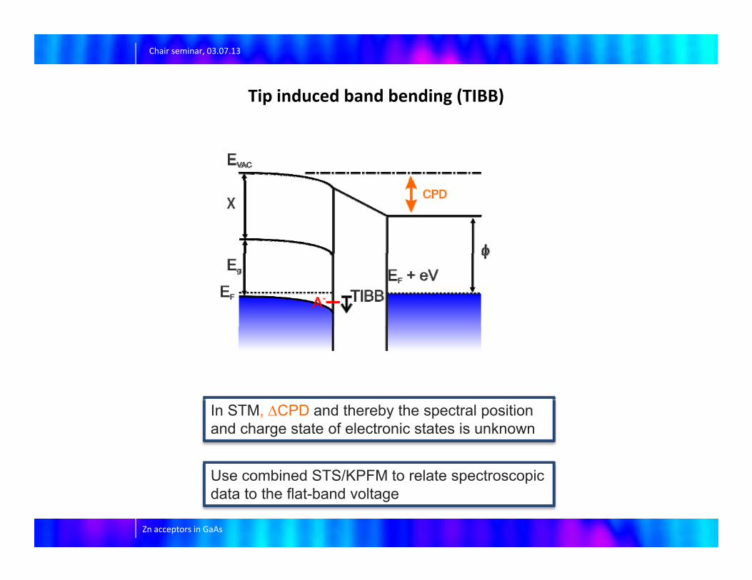
Chair seminar, 03.07.13
1 Cleavage1. Cleavage2. Surface properties affecting impurities3. Tip impact - TIBB
Zn acceptors in GaAs
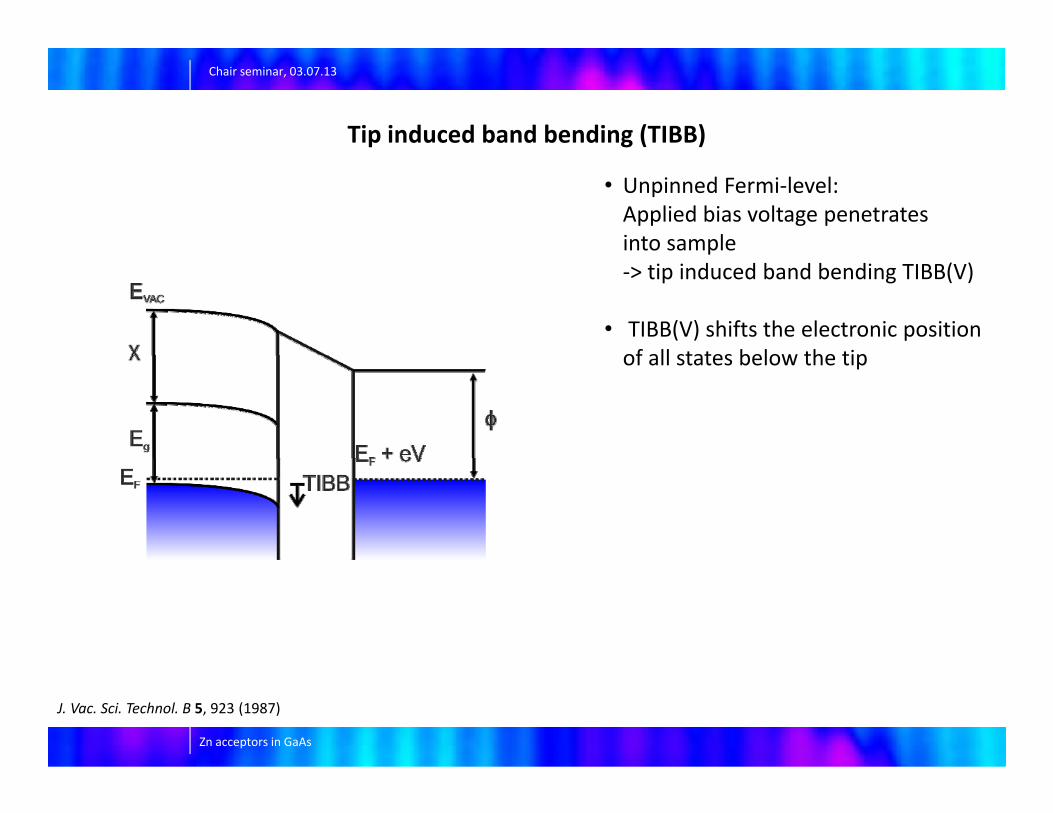
Chair seminar, 03.07.13
Tip induced band bending (TIBB)
• Unpinned Fermi‐level: Applied bias voltage penetrates into samplep‐> tip induced band bending TIBB(V)
• TIBB(V) shifts the electronic position of all states below the tipof all states below the tip
Zn acceptors in GaAs
J. Vac. Sci. Technol. B 5, 923 (1987)

Chair seminar, 03.07.13
Tip induced band bending (TIBB)
• Unpinned Fermi‐level: Applied bias voltage penetrates into samplep‐> tip induced band bending TIBB(V)
• TIBB(V) shifts the electronic position of all states below the tipof all states below the tip
• Electronic state can be shifted across the Fermi‐level: Change of occupation A‐/0, change of contribution to tunneling
• TIBB(V) is non‐zero even for zero• TIBB(V) is non‐zero even for zero bias, due to the contact potential difference ΔCPD between tip and sample
TIBB(V) can be negative for positive V, andTIBB(V = ΔCPD/e) = 0
Zn acceptors in GaAs
J. Vac. Sci. Technol. B 5, 923 (1987)
( )

Chair seminar, 03.07.13
Tip induced band bending (TIBB)
V < VCPD V = VCPD V > VCPD
• If applied bias voltage cancels difference in work function between tip and sample, pp g p pthe bands are flat: TIBB(V = CPD/e = VCPD) = 0; State is at the Fermi level
• V < VCPD: State is located below the Fermi level
V > V St t i l t d b th F i l l
Zn acceptors in GaAs
• V > VCPD: State is located above the Fermi level

Chair seminar, 03.07.13
Tip induced band bending (TIBB)
In STM, CPD and thereby the spectral position and charge state of electronic states is unknown
Zn acceptors in GaAs
J. Vac. Sci. Technol. B 5, 923 (1987)
Chair seminar, 03.07.13
Tip induced band bending (TIBB)
In STM, ΔCPD and thereby the spectral position and charge state of electronic states is unknown
Use combined STS/KPFM to relate spectroscopic
Zn acceptors in GaAs
Use combined STS/KPFM to relate spectroscopic data to the flat-band voltage

Chair seminar, 03.07.13
Electronic properties the GaAs(110) surface
• 4 surface resonances outside the band gap
• Fermi‐level not pinned:‐> tunneling is only possible
for certain bias voltages‐> bulk DOS is not masked
Zn acceptors in GaAs
calculated DOS: Phys. Rev. Lett. 77, 2997 (1995)

Chair seminar, 03.07.13
Electronic properties of Zn doped GaAs
• Zn is an acceptor in GaAs‐> p‐type doping
• Zn ionization energy in GaAs:• Zn ionization energy in GaAs: 31 meV
• For the dopant concentration 1 ∙ 1019 Zn/cm3 used hereimpurity band of ΔEIB = 24 meVwidth is established
Zn acceptors in GaAs
E. F. Schubert: Doping in III‐V Semiconductors,Cambridge University Press, 1993

Chair seminar, 03.07.13
Electronic properties of Zn doped GaAs
Zn acceptors in GaAs

Chair seminar, 03.07.13
Electronic properties of Zn doped GaAs
Zn acceptors in GaAs

Chair seminar, 03.07.13
Literature Review: Zn in GaAs
→mapping of→ mapping of excited acceptor state
Zn acceptors in GaAs

Chair seminar, 03.07.13
Literature Review: Zn in GaAs
Zn acceptors in GaAs

Chair seminar, 03.07.13
Literature Review: Zn in GaAs
Zn acceptors in GaAs

Chair seminar, 03.07.13
Literature Review: Zn in GaAs
Zn acceptors in GaAs

Chair seminar, 03.07.13
Literature Review: Zn in GaAs
Zn acceptors in GaAs

Chair seminar, 03.07.13
Literature Review: Zn in GaAs
Zn acceptors in GaAs

Chair seminar, 03.07.13
Literature Review: Zn in GaAs
Zn acceptors in GaAs

Chair seminar, 03.07.13
Literature Review: Zn in GaAs ‐ Summary
In gap acceptor related enhanced current and conductance is observed
All papers either guess the tip’s work function or extract it from I(z), which is known
In‐gap acceptor‐related enhanced current and conductance is observed.
to give only a rough estimate for Φtip (J. Phys. Chem. C. 113, 11301 (2009)).
The explanations given are based on single particle pictures of transport.
However: In using combined X‐STM/AFM, we have an exact method to determine the tip’s work function: KPFMthe tip s work function: KPFM
Zn acceptors in GaAs

Chair seminar, 03.07.13
Kelvin Probe Force Microscopy (KPFM)
• Energy of capacitor: 2
21 VCE ⋅=
V: voltage drop between tip and sample
BiasVeCPDV += /
• frequency shift
• df(V) is parabolic in V:
Ezz
Fdf2
2
∂∂
−=∂∂
=
df(V) is parabolic in V:
h f h b l
2
2
2
)/(21
BiasVeCPDzC
zFdf +⋅
∂∂
−=∂∂
=
Setpoint: U = 50 mV I = 2 5 pA • the maxima of the parabola is located at:
eCPDVBias /−=→ the maximum in KPFM
Setpoint: Ubias = 50 mV, I = 2.5 pA, Δz = ‐5 Å, Aoszi = 1 Å
Zn acceptors in GaAs
signal corresponds to CPD Appl. Phys. Lett. 58, 2921 (1991)

Chair seminar, 03.07.13
Dual sample holder
tuningfork
wafer
Cu‐crystal
Cu single‐crystal and wafer are accessible within one experiment.
Zn acceptors in GaAs

Chair seminar, 03.07.13
From KPFS we determine VC for aFrom KPFS, we determine VCPD for a particular tip apex, VCPD = 0.64 V
Zn acceptors in GaAs

Chair seminar, 03.07.13
From KPFS we determine VC for aFrom KPFS, we determine VCPD for a particular tip apex, VCPD = 0.64 V
Calculate TIBB(V), using a Poisson equation solver with VCPD as input
Zn acceptors in GaAs

Chair seminar, 03.07.13
From KPFS we determine VC for aFrom KPFS, we determine VCPD for a particular tip apex, VCPD = 0.64 V
Calculate TIBB(V), using a Poisson equation solver with VCPD as input parameterparameter
STS related to the flat-band voltage
Enhanced Acceptor related current is present in negative, zero and positive TIBB regimesg
Zn acceptors in GaAs

Chair seminar, 03.07.13
V < VCPD V = VCPD V > VCPD
Constant-height dI/dV maps reveal a similar triangular feature of enhancedConstant-height dI/dV maps reveal a similar triangular feature of enhanced conductance in negative, zero and positive TIBB regimes
One conduction mechanism in active in all three band bending regimes
Zn acceptors in GaAs

Chair seminar, 03.07.13
The {110} surfaces of GaAs
id iside‐view
top‐viewp
Zn acceptors in GaAs

Chair seminar, 03.07.13 Sample System
Crystallographic properties of GaAs
GaAs: III‐V semiconductor, zinc‐blende lattice structure. (110) surface prepared by cleaving of wafer consists of
Zn acceptors in GaAs
(110) surface: prepared by cleaving of wafer, consists ofalternating rows of As and Ga atoms

Chair seminar, 03.07.13 Sample System
Electronic properties of GaAs(110)
• 4 surface resonances outside the band gap
A5Ubias = ‐ 0.5 V
band gap
• Fermi‐level not pinned:‐> tunneling is only possible C3
for certain bias voltages‐> bulk DOS is not masked
• Resonances have the same spatial
Ubias = + 1.6 V
Resonances have the same spatial periodicity as surface unit cell
• A5 and C4: rows di l [001]
C4Ubias = + 2.2 V
calculated DOS: Phys. Rev. B 20, 4150 (1979)
perpendicular to [001]C3: rows parallel to [001]
Zn acceptors in GaAs

Chair seminar, 03.07.13
Bulk vs Foremost acceptorsBulk vs. Foremost acceptors
SPM tip
Foremost acceptors
Zn impurityBulk
acceptors
GaAs
Zn acceptors in GaAs

Chair seminar, 03.07.13
The Hamiltonian for the junctionThe Hamiltonian for the junction
ForemostSubstrate:lk
Metallic tip
TunnellingForemost acceptors (FA)
Interacting electrons
Anderson‐Hubbard
Bulk acceptors + semiconductor
Non‐interacting electrons with
energy dependent
Metallic tip
Non‐interacting electrons with flat
DOS
Tunnellingbetween
previous blocks
Single particleGeometrical
modelenergy dependent
DOSencoded
Zn acceptors in GaAs

Chair seminar, 03.07.13
Anderson‐Hubbard modelAnderson‐Hubbard model
Zn acceptors in GaAs

Chair seminar, 03.07.13
Anderson‐Hubbard modelAnderson‐Hubbard model
We considered 5 acceptor states
The number of states in the Fock space of the system i 45 1024is 45 = 1024
The system Hamiltonian is particle-hole symmetric
In equilibrium: Number of electrons = number of impurities
Constant terms in the interaction: positive ions at the acceptor sites
Charge neutrality is accounted for
Zn acceptors in GaAs

Chair seminar, 03.07.13
Spectrum of the Anderson‐Hubbard HamiltoniansSpectrum of the Anderson Hubbard Hamiltonians
U = 10|t|U = |t|
t = -1 meV
[eV]
[eV]
U = 5|t| U = 50|t|
[eV] [eV]
Particle-hole symmetry
Zn acceptors in GaAs
y yInterplay of the hopping and charging dynamics for U ≤ 10|t|

Chair seminar, 03.07.13
Leads modelingLeads modeling
Inelastic effects
2 02.0
1.0
Flat density of states
A t C d tV l
0.0
Acceptorsband
Conductanceband
Valence band
Free electron gas with: Free electron gas with: Chemical potential µ0Temperture T
Chemical potential µ0- eVbTemperture T
Zn acceptors in GaAs

Chair seminar, 03.07.13
Transport: master equation approachTransport: master equation approach
ncanon
ical
energy
EGra
ParticleNumber
M M + 1 M ‐ 1
ParticleNumber
Zn acceptors in GaAs

Chair seminar, 03.07.13
Tunnelling rates Bias dependentTunnelling rates
The many-body rates read
And contain the energy dependent single particle rates
Bias dependentDelocalization of the substrate
Localization of the tip tunnellingto the last impurity
Bias dependentDelocalization of the substratetunnelling
Extreme asymmetry in the coupling
Estimated from the current
Zn acceptors in GaAs

Chair seminar, 03.07.13
Average currentAverage current
The average stationary current through the junction is calculated as:
where one obtains due to charge conservation:
Zn acceptors in GaAs

Chair seminar, 03.07.13
Current and differential conductanceCurrent and differential conductance
Zn acceptors in GaAs

Chair seminar, 03.07.13
Basic observationsBasic observations
Current flows through the system at Vb > 0 only if N5<2
At U = 0 the width of the current step is given by 4|t|/α
At U > 0 a plateau develops around zero band bendingAt U > 0 a plateau develops around zero band bending, which increases with the strength of the interaction
The finite current region becomes wider in presence of the interaction
Reacher conduction structure appears in presence of the interaction
αinteraction
Zn acceptors in GaAs

Chair seminar, 03.07.13
Impurities occupations and many‐body states populationsImpurities occupations and many body states populations
Zn acceptors in GaAs

Chair seminar, 03.07.13
ConclusionsConclusions
Due to the strong asymmetry between the tip and substrate coupling
the system is always almost in equilibrium
The current plateau around the zero band bending reflect the resistance of theThe current plateau around the zero band bending reflect the resistance of the
system to charging , thus the size U/α
A rich variety of peak structures in the differential conductance indicates the
interplay between the coupling between the impurities and the charging energy
An even richer variety expected for a more realistic 3D network of foremost
i iti h i it h diff t t !impurities: each impurity has a different spectrum!
Zn acceptors in GaAs

Chair seminar, 03.07.13
Thank you for your attention !
Zn acceptors in GaAs