Abstract Site-Controlled III-Nitride Quantum Dots
136
Site-Controlled III-Nitride Quantum Dots by Leung Kway Lee A dissertation submitted in partial fulfillment Of the requirements for the degree of Doctor of Philosophy (Electrical Engineering) in The University of Michigan 2011 Doctoral Committee: Assistant Professor Pei-Cheng Ku, Chair Professor Rachel S. Goldman Professor Lingjie Guo Professor Jasprit Singh Assistant Professor Hui Deng
-
Upload
truongxuyen -
Category
Documents
-
view
213 -
download
0
Transcript of Abstract Site-Controlled III-Nitride Quantum Dots

Site-Controlled III-Nitride Quantum Dots
by
Leung Kway Lee
A dissertation submitted in partial fulfillment Of the requirements for the degree of
Doctor of Philosophy (Electrical Engineering)
in The University of Michigan 2011
Doctoral Committee: Assistant Professor Pei-Cheng Ku, Chair Professor Rachel S. Goldman Professor Lingjie Guo Professor Jasprit Singh Assistant Professor Hui Deng

© Leung Kway Lee
All Rights Reserved 2011

ii
To my family

iii
Acknowledgements
I would like to sincerely thank my advisor Prof. P.-C. Ku for his guidance,
support and patience during my doctoral study. He not only taught me how to do
research, but also showed me the correct attitude to deal with difficulties – always think
what you can do, and never run away from the problems – which made me stick to the
challenge of site-control nanostructures. In addition, I want to thank my thesis
committees – Prof. Goldman, Prof. Guo, Prof. Deng and Prof. Singh -- for their valuable
and professional advices on a variety of subjects, ranging from material growth,
fabrication techniques, optical measurement, to quantum dot simulations.
In the field, I feel that experimental work is usually not the work of an individual,
but the combination of multiple efforts, so I owe deep thanks to the co-workers around
me: I would like to thank my colleague Michael Kuo, who shared a great deal of the
painstaking work of material growth, and made MOCVD maintenance less painful; many
of the advanced optical characterizations would be impossible without the effort of Lei
Zhang, who continues to produce useful results from the single-dot experiments; last but

iv
not least, I would like to thank my colleague Chu-Hsiang Teng for continuing and
improving on the electrodeposition shrinkage technique.
My research topic is highly fabrication-oriented so it would not have survived if
there were not a good cleanroom facility. Because of this, I would like to thank all the
cleanroom staff for maintaining an efficient and user-friendly working environment.
Especially, on behalf of all the crystal growers in the SSEL, I would like to sincerely
thank, again, Mr. Dennis Schweiger, for his humorous, resourceful and swift response to
our epitaxial crisis; As for specific cleanroom tools, I am grateful to Greg Allion, Brian
van der Elzen, Matthew Oonk and Pilar Herrera-Fierro for their help on the work related
to nanofabrication.
Finally, I would like to thank my family. Without their unconditional love and
support, I could not have completed this phase of my life.

v
Table of Contents
Dedication………………………………………………………………………………...ii
Acknowledgements……………………………………………………………..……….iii
List of Figures…………………………………………………………………….……viii
List of Tables………………………………………………………………………...…xiii
List of Abbreviations………………………………………………………………..…xiv
Abstract………………………………………………………………………………..xvii
Chapter
1. Introduction…………………………………………………………...………….…..1
1.1 Semiconductor Quantum Dots for Photonics Applications………………….……1
1.2 III-Nitride Quantum Dots……………………………………………....….…...…3
1.3 The Quantum-Dot-Cavity System………………………………………….….….4
1.4 Site- and Dimension-Control for III-Nitride Quantum Dots…………….…….….5
1.5 Objective and Organization of this Thesis……….………....................................11
2. Selective Area Epitaxy for III-Nitride Nanostructures..……….………………...15
2.1 Selective Area Epitaxy for III-Nitride Materials…………………………...……16
2.1.1 Overview…………………………………………………………………16

vi
2.1.2 Modeling of Selective Area Epitaxy for Micro- and Nano-Structure Growth…………………………………………………………………...19
2.2 Prior Work of III-Nitride Nanostructures using Selective Area Epitaxy………...27
2.3 General Patterning Technique for Nanoscale SAE…………………………..…..28
2.4 Phase-Field Model and Growth Morphology Evolution…………………...……32
2.5 Fabrication of Site-Controlled InGaN Quantum Dots………………………..….36
2.6 Summary…………………………………………………………………...…….37
3. III-Nitride Quantum Dots Using Reactive-Ion Etching………………….………39
3.1 Overview of Top-Down Etching Approach…………………………………...…40
3.2 Prior Work of III-Nitride Nanostructures Using Top-Down Etching…..………..42
3.3 InGaN Single Quantum Well Epitaxy…………………………………………...42
3.4 Fabrication of Site-Controlled InGaN Quantum Disk………………….………..44
3.5 Summary……………………………………………………………….………...48
4. Optical Properties of Site-Controlled III-Nitride Quantum Dots….……………49
4.1 Setup for Optical Characterization……………………………………………….49
4.2 InGaN Quantum Dots Using Selective Area Epitaxy………………..…..………51
4.2.1 Room-Temperature Photoluminescence…………………………………51
4.2.2 Influence of the Morphology on Photoluminescence…………………....53
4.3 InGaN Quantum Disk Using Top-Down Etching………………………………..55
4.3.1 Room-Temperature Photoluminescence………………………………....55
4.3.2 Diameter-Dependent Photoluminescence………………………………..59
4.3.3 Temperature-Dependent Photoluminescence……………………………64
4.4 Summary……………………..…………………………………………………..67

vii
5. Integration of III-Nitride Optical Cavity………..……………………………...…68
5.1 Integration of III-nitride Nanostructures into an Optical Cavity………………...69
5.2 Etching of III-Nitride Semiconductors…………………………………….……70
5.3 Suspended III-nitride Optical Cavity…………………………………………….71
5.3.1 Bandgap-selective Photo-electro-chemical (PEC) Etching …….….……71
5.3.2 Experiment and Results………………………………………………….72
5.4 Summary………………………………….……………………………………...77
6. Scalable and High-Throughput Nanopatterning Techniques……….………..…78
6.1 Nanometer-Scale Patterning………………………………………..……….…...79
6.2 Challenges for the Mask Shrinkage Techniques………………….……………...85
6.3 Wafer-Scale Nanopatterning using Electrodeposition………….………………..86
6.4 Challenges for the Electrodeposition Shrinkage Technique…….………….……97
6.5 Summary…………………………………………………………………………97
7. Conclusions and Future Work…………………………..…………………..……..99
7.1 Research Summary………………….………......………………………...…......99
7.2 Future Work……………………………………….…...………………………103
Bibliography…………………………………………………………………...………105

viii
List of Figures
Fig. 1-1 Atomic force microscopy topography of a single InAs QD embedded inside a GaAs photonic crystal slab optical cavity [164]………………………..……..5
Fig. 1-2 Graphical interpretation of the reported dot sizes and densities listed in Table
1-1……………………………………………………………………………..9 Fig. 2-1 Scanning electron micrographs (SEMs) of epi-structures formed by SAE.
Different lithographic tools (contact aligners, stepper and e-beam lithography) were used to pattern openings across the length-scale on the masking layer…………………………………………………………………………..17
Fig. 2-2 Source supply mechanisms during selective area epitaxy……….…………..21 Fig. 2-3 Growth rate anisotropy of different crystal planes during selective area epitaxy
using MOCVD [35,46]…………………………………………………...….23 Fig. 2-4 A simple model to trace the evolution of crystal facets taking into
consideration the effect of growth rate anisotropy……………………..……25 Fig. 2-5 The plot of ( )θR entered as empirical data……………………………...…..25 Fig. 2-6 A trench or a pit with 45° sidewall on the z-plane of a crystal. Growth rate
anisotropy makes the inclined facets grow faster and coalesce, filling the void. Only the slower-growing z-plane remains after extended amount of growth time……………………………………………………………………….….26
Fig. 2-7 Exaggerated facet-angle-dependent growth rate used in the simulation shown
in Fig. 2-6. Facets with angle greater than 70° are assigned a slower growth rate compared to the less-tilted facets; because of this, slowest growing facets/planes dominate the final profile as the tilted facets coalesce,
ix
demonstrating and validating the effect of growth rate anisotropy using the simple point-tracking model……………………………………………..…..27
Fig. 2-8 Illustration of the process flow of nanoscale SAE (NSAE)………...………..29 Fig. 2-9 (a) Dot openings on SiO2 mask using Ar flow of 15 sccm in RIE. (b) Dot
openings on SiO2 mask using Ar flow of 5 sccm in RIE………………...…..31 Fig. 2-10 SEM image of GaN nanodot array grown by SAE. The image was taken after
the removal of the SiO2 SAE mask. The inset shows nanoholes in SiO2 with diameter of 25 nm after patterning………………………………………...…32
Fig. 2-11 The left column shows the SEM images taken at the different stages of the
nanoscale SAE and the right shows the calculated morphology. The scale bars on the left and on the right are 50 and 40 nm, respectively………...………..34
Fig. 2-12 (Left) Tiled SEM image of the SAE InGaN QD array after the regrowth of the
final capping layer. (Right) SEM top-view of the same QD array…….…….37 Fig. 3-1 Illustration of the top-down approach………………………………………..40 Fig. 3-2 Room-temperature photoluminescence of an InGaN SQW grown by
MOCVD. Laser excitation wavelength used is 390 nm..……………………44 Fig. 3-3 Illustration of the process flow. Nanopillars are made from a patterned InGaN
SQW by reactive-ion etching.………………………………………………..45 Fig. 3-4 (a) SEM image of a patterned area where single-disk µ-PL is performed. The
four microscale square patterns are used as marks for quickly locating the single pillar during optical measurement. The inset shows the tilted SEM image of a 17-nm-diameter single disk after removal of Cr nanodot etch mask (b) A square array of 17-nm-diameter quantum disks, with an array pitch of 300 nm. (c) SEM documentation of the average disk diameter of across a series of patterns which were written by a graded e-beam dose……..………47
Fig. 4-1 Illustration of the setup used for measuring photoluminescence (PL) from site-
controlled InGaN QDs. This setup is compatible with both macro- and micro-PL…………………………………………………………………………….51
Fig. 4-2 SEM images of the InGaN quantum disk arrays fabricated by (a) nanoscale
SAE and by (b) top-down etching. Insets are the zoomed-in SEM view of individual nanostructure in the arrays; both scale bars in the insets represent 50 nm. (c) Room-temperature PL spectra of the InGaN quantum disk arrays (104 dots illuminated) fabricated by the two approaches………………………………………………...………………….53

x
Fig. 4-3 Room-temperature photoluminescence spectrum and the calculated
photoluminescence spectrum of the InGaN nanodot array. The calculated PL spectrum is based on the calculated InGaN layer thickness profile shown in the inset. The two lines in the inset represent the InGaN/GaN boundaries……………………………………………………………………55
Fig. 4-4 (a) The SEM image of a single site-controlled InGaN quantum disk of a
diameter of 17 nm. (b) CCD image of a single quantum disk emission at room-temperature. (c) Room-temperature PL spectrum of a single quantum disk compared to unetched QW (measured) as well as calculated QD and QW emission……………………………………………………….……………..57
Fig. 4-5 Photoluminescence spectrum of a 17-nm-diameter single InGaN quantum disk
(the same one shown in Fig. 4-4) compared to the calculated QD and QW spontaneous emission at 75 K………………………………………..………58
Fig. 4-6 Room-temperature PL of an ensemble of 1024 InGaN quantum disks……...59 Fig. 4-7 The relative peak emission energy of single InGaN quantum disks with
diameters of 16, 21 and 25 nm as compared to two different models: the particle-in-the-box model and the model used in this work (2D Poisson equation)……………………………………………………………………..60
Fig. 4-8 PL peak energy of single InGaN quantum disk as a function of the disk’s
diameter which varies from 2 μm to 37 nm………………………...………..61 Fig. 4-9 (a) The calculated band diagram of a 16-nm-diameter, fully-depleted pillar
and the corresponding ground conduction and valence band states. (b) The calculated space charge density distribution of a 20-nm-diameter nanopillar with a doping concentration of 1017 cm-3 (n-type) covered by a 40-nm-thick Al2O3 layer…………………………………………………………..……….62
Fig. 4-10 Illustration of the Poisson model in cylindrical coordinates (2D) used to
calculate the potential profile in the InGaN disk plane………………………63 Fig. 4-11 (a) The measured peak emission energy versus temperature (squares) and the
fitting by Varshni’s model (solid line). (b) Arrhenius plot of the integrated PL intensity. (c) FWHM linewidth versus temperature (squares) and the fitting based on equation (1) (red line)………………………………………...……66
Fig. 5-1 Illustration of the concept behind the PEC process………………...………..71

xi
Fig. 5-2 The left shows the low-indium (2 and 4 %) InGaN superlattice used in the PEC etching experiment. The right shows a tilted SEM image of the sidewall formed by etching in order to expose the InGaN SL to the electrolyte…..….73
Fig. 5-3 Illustration of the setup used for PEC etching. To withstand high acidity, both
the container and the sample holder are made of Teflon…………...….…….74 Fig. 5-4 Tilted SEM of undercut after PEC etching. Residual nanoscale whiskers were
observed. The bottom edge of the membrane is wiggly with peak-to-peak fluctuation of ~ 100 nm…………………………………………...………….75
Fig. 5-5 Tiled SEMs showing the undercuts after PEC etching of InGaN SL grown on
a commercial GaN template (Kyma Technology). Whisker density was reduced and a smooth bottom edge of the GaN membrane was observed…..76
Fig. 6-1 Illustration of the sub-10 nm patterning technique using atomic layer
deposition (ALD).…………………..………………………………………..81 Fig. 6-2 (a) Original nanoscale apertures. (b) The diameter of the apertures are shrunk
to 7 nm after ALD and ICP-RIE. (c) An array of apertures with graded diameters from 16 to 10 nm, from left to right, were formed after ALD and ICP-RIE pattern shrinkage………………………………………………..….83
Fig. 6-3 The formation of gold nanoparticle array after lift-off verified the through etch
of the final ICP-RIE step. Because the sample is designed for SAE, the non-ideal sidewall angle results in slight non-uniformity of gold particle sizes………………………………………………………………..………....84
Fig. 6-4 Illustration of the proposed (a) electrodeposition and (b) electroetching
processes for wafer-scale nanopatterning. (i) In electrodeposition, the high conductivity metallic layer is connected to the cathode while in electroetching, it is connected to the anode as represented by the current flow directions. (ii) In both processes, the samples are immersed in an electrolyte in which either the metal cations are reduced to or the metal atoms are oxidized from the metallic surface. Thus microscale space and line features can be shrunk to nanoscale by electrodeposition and electroetching, respectively. (iii) The shrunk features can be readily transferred to the underlying substrate by etching and the removal of the metal layers. (c) Illustration of the electrodeposition setup used in this work. The sample is coated with a metallic layer with microscale patterns and is connected to the cathode of a current source. Temperature and circulation are controlled by a hotplate with feed-back sensors………………………………….………………………………89
Fig. 6-5 Scanning electron micrograph (SEM) of the metallic trench features after
different electrodeposition times. Both the top and the cross-sectional views

xii
are shown. The original base width of the trench is 710 nm. The base widths were shrunk to 515 nm, 290 nm and 80 nm, after 8-, 15-, and 19-minute of electrodeposition, respectively……………………………………………….91
Fig. 6-6 (a) The plot of base width of the trenches and the thickness deposited on the
top of the gold film against the electrodeposition time. The base width and deposition thickness are measured from the cross-sectional SEM images shown in Fig. 6-5. (b) The plot of deposition rate on the sidewall and on top of the metal film against the electrodeposition time. The deposition rate is calculated from the fitted curves associated with the data shown in Fig. 6-6 (a)………………………………………………………………………...…..93
Fig. 6-7 SEM of the trench feature transferred to a 20-nm-thick silicon dioxide film
using reactive ion etching. (a) Top view after electrodeposition. (b) Top view after reactive ion etching of SiO2 and the removal of chromium and gold films. The base widths of the trench are 80 nm and 93 nm before and after the pattern transfer. The etch bias is 13 nm……………………………………..95
Fig. 6-8 SEM of the shrunk circular openings in a gold film. The diameter of the
circular openings after lift-off is 680 nm (not shown), which became 100 nm after 13-min of electrodeposition…………………………………………….96

xiii
List of Tables
Table 1-1 A summary of size and density of self-assembled InGaN QDs reported in the literature…………………………...…………………………………………..7
Table 3-1 A summary epitaxial steps used to grow InGaN SQW. The SQW is regrown
on a GaN template, grown on a sapphire substrate by our MOCVD system………………………………………………………………………..43

xiv
List of Abbreviations
0D Zero-Dimensional
1D One-Dimensional
2D Two-Dimensional
3D Three-Dimensional
ALD Atomic Layer Deposition
BHF Buffered Hydrofluoric Acid
CCD Charge-Coupled Device
DBR Diffractive Bragg Reflector
DFB Distributed Feedback Reflector
EBL Electron-Beam Lithography
ELOG Epitaxial Lateral Overgrowth
FWHM Full Width At Half Maximum
GaAs Gallium Arsenide
GaN Gallium Nitride
GaOx Gallium Oxide

xv
HCG High-Contrast Grating
HVPE Hydride Vapor Phase Epitaxy
ICP Inductively-Coupled Plasma
InGaN Indium Gallium Nitride
LHe Liquid Helium
LER Line Edge Roughness
MOCVD Metalorganic Chemical Vapor Deposition
MOVPE Metalorganic Vapor Phase Epitaxy
MBE Molecular Beam Epitaxy
MEM Microelectromechanical
MQW Multiple Quantum Well
NH3 Ammonia
PL Photoluminescence
PEC Photoelectrochemical
PECVD Plasma-Enhanced Chemical Vapor Deposition
PhC Photonic Crystal
PMMA, (C5O2H8)n Poly(methyl methacrylate)
QD Quantum Dot
QW Quantum Well
RIE Reactive-Ion Etching
RT Room Temperature
SA Self-Assembled
SAE Selective Area Epitaxy

xvi
SCC Sidewall Charge Center
SEM Scanning Electron Microscopy
SK Stranski-Krastanov
SL Superlattice
SQW Single Quantum Well
SBM Smoothed Boundary Method
TRPL Time-Resolved Photoluminescence
TMG, Ga(CH3)3 Trimethylgallium
TMI, In(CH3)3 Trimethylindium
UID Unintentionally-Doped
VRS Vacuum Rabi Splitting
YBE Yellow Band Emission
ZMW Zero-Mode Waveguide
xvii
Abstract
Site-Controlled III-Nitride Quantum Dots
by
Leung Kway Lee
Chair: Pei-Cheng Ku
Group III-nitride semiconductor quantum dots (QDs) exhibit large exciton
binding energy (> 26 meV) and band offsets, making them an ideal candidate to exploit
various quantum optical effects at the high temperature including single-photon emission,
strong-coupling, indistinguishable photon generation and polariton lasing. These
phenomena can lead to future quantum information technology. The practical use of the
III-nitride QDs as quantum light sources requires the addressability of a single QD, both
in its position and emission energy. To date, most semiconductors QDs are epitaxially
grown by the self-assembled processes such as the Stranski-Krastanov growth which
possess very limited control over the QDs’ positions and dimensions, making them
difficult to be utilized at the device level.

xviii
In this thesis, we investigate novel processes for the fabrication of site- and
dimension-controlled III-nitride QDs. Two lithography-based techniques have been
considered including selective area epitaxy (SAE) and top-down etching. In SAE, the
formation QDs is controlled by the pre-patterned mask openings. Different source supply
and growth mechanisms determine QD’s growth morphology. Morphology evolution in
SAE is studied experimentally which qualitatively agrees with the theoretical phase-field
model. The non-uniformity of the InGaN thickness was found to be the origin of the
broad photoluminescence (PL). In the top-down etching approach, InGaN QDs are
formed by etching a patterned InGaN single quantum well. Each QD is disk-shaped and
embedded in a nanopillar. Strong and distinct PL signal of a single quantum disk was
observed even at room temperature. The emission was found to exhibit characteristics
from a discrete energy state that is homogeneously broadened. The single InGaN QD was
extensively studied using micro-PL. A model based on 2-dimensional Poisson’s equation
was developed to quantitatively explain the large blue shift observed in the experiment.
The saturation of the PL linewidth at high temperatures was also interpreted using a
sidewall charge center model.
To demonstrate the scalability and device integration of the site-controlled III-
nitride QDs, large-area nanolithographic processes and photonic-crystal optical cavities
have been developed. Pattern shrinkage by spacer and by electrodeposition were
introduced and demonstrated, with the former aiming at sub-10 nm patterning and the
latter at large-scale nanofabrication.

1
Chapter 1
Introduction
1.1 Semiconductor Quantum Dots for Photonics Applications
Quantum dots (QDs) are artificial nanostructures in which electron energy levels
are quantized as in natural atoms. QDs share many similar properties as atoms yet can be
made and engineered artificially. Hence QDs have been often coined as artificial atoms.
Since the experimental realization of quantum dots in the 80’s, they have opened up a
new frontier in nanoscience and engineering, providing a variety of technological
applications ranging from a new class of electronic and optoelectronic devices, biological
applications, to quantum science.
Due to the quantization of electron energy, only two electrons (the factor of two
comes from the spin degeneracy) can occupy each discrete energy level at a given time,
resulting in a discrete, delta-function-like density of states. This property has profound
impacts on photonic devices. As an example, a semiconductor laser requires the
2
separation of the quasi-Fermi levels for the electrons and holes to at least exceed the
photon energy (i.e. population inversion). The use of QDs can allow this condition to be
reached at a lower carrier concentration, reducing the threshold current. Because of the
discrete, delta-function-like density of states, the ground state of a QD can only be
occupied with at most two excitons. This limit on the exciton population affects the
ground-state emission of the single quantum dot – the emission can be regulated in a
stream of individual photons. Hence a single QD can act as a single-photon source
[1,2,3,102]. When a QD holds two interacting excitons (through Coulombic interaction),
the formation of biexcitons can potentially lead to the emission of entangled photon pairs
[2,3]. The capability of a single QD to quantize its emission has made it a subject of
pursuit for semiconductor quantum light source with high interest. Quantum light sources
as such will become the building blocks for quantum cryptography, quantum computing,
quantum information processing and quantum communication [1,2,3,4].
Other applications of QD as a semiconductor light source include the ultrafast
speed of modulation. Single QD emitters can be electrically modulated at an extremely
high speed [5]. The modulation speed of a semiconductor emitter without optical
feedback (e.g. a light-emitting diode) scales inversely with the square root of the emitter
volume. Hence a QD embedded in a plasmonic cavity can be an ideal structure for
terahertz speed modulation. Together with nonlinear optical materials, QDs can be a
fundamental building block for next-generation optical signal processing on the chip.
It is important to note that, the continuing scaling and monolithic integration of
optical components will eventually lead to the demand of nanoscale semiconductor light
source. To that end, semiconductor QDs will be the ideal candidate.

3
1.2 III-Nitride Quantum Dots
Semiconductor QDs can be made from different systems of materials e.g. III-V,
II-VI and III-nitride semiconductors. From the practical view-point of a light source, a
QD should be have high radiative efficiency even without cryogenic cooling (below 77
K), which severely limits the device’s portability and raises its operation cost. Aiming at
non-cryogenic operation of a QD light source, the focus has landed on III-nitride
semiconductors. Group III-nitride (GaN, AlN, InN) and related alloys exhibit direct
bandgaps covering ultraviolet, visible, and near-infrared spectrum. The successful
development of III-nitride pn-junctions in the early 90’s has enabled a rapid development
of III-nitride photonic devices including the commercialization of short-wavelength laser
diodes and light-emitting diodes. Compared to III-V semiconductors (e.g. GaAs and InP),
III-nitride materials possess many unique properties such as larger oscillator strength
[6,7], larger exciton binding energy [9,10], lower surface state densities [11], larger band
offset, and robust spin coherence [12]; the exciton binding energy is larger than the
thermal energy kB•(300 K) = 26 meV, which means that for III-nitride materials can have
excitonic effects up to room temperature; the exciton binding energy increases with the
dimensionality of quantum confinement [8,9], implying an enhanced excitonic effect for
III-nitride quantum wells (QWs) and even more for III-nitride QDs. Together with a large
oscillator strength and a large band offset (better quantum confinement), III-nitride
semiconductors are ideal for quantum structures (QWs and QDs) that exhibit highly
efficient quantum optical effects at higher temperatures. Indeed, strong light-matter
interactions have been observed in GaN and InGaN microcavities up to room temperature

4
[6,13]; single-photon emission has been observed in GaN/AlN QDs up to 200K [102].
On the other hand, because of much larger effective masses for both electrons and holes
and hence a larger density of states in a finite-dimensional structure, III-nitride quantum
dots devices are expected to provide a much greater improvement over their quantum
well counterparts. Because of these advantages, III-nitride QDs are deemed one of the
most prominent candidates for realizing room-temperature quantum light source.
1.3 The Quantum-Dot-Cavity System
By placing a quantum dot precisely at the anti-node of the electric field inside an
optical cavity, one can leverage the weak (Purcell) or strong coupling effect to greatly
improve the directionality and the efficiency of the QD emission – the as-resulted
quantum light source will have much higher extraction efficiency, pushing them a bit
closer to the practical use [1,3]. Because of this, all the studies of QD-related quantum
light source all include the integration of a QD into certain optical cavity, to form the
QD-cavity system. The QD-cavity system has become the standard blueprint for
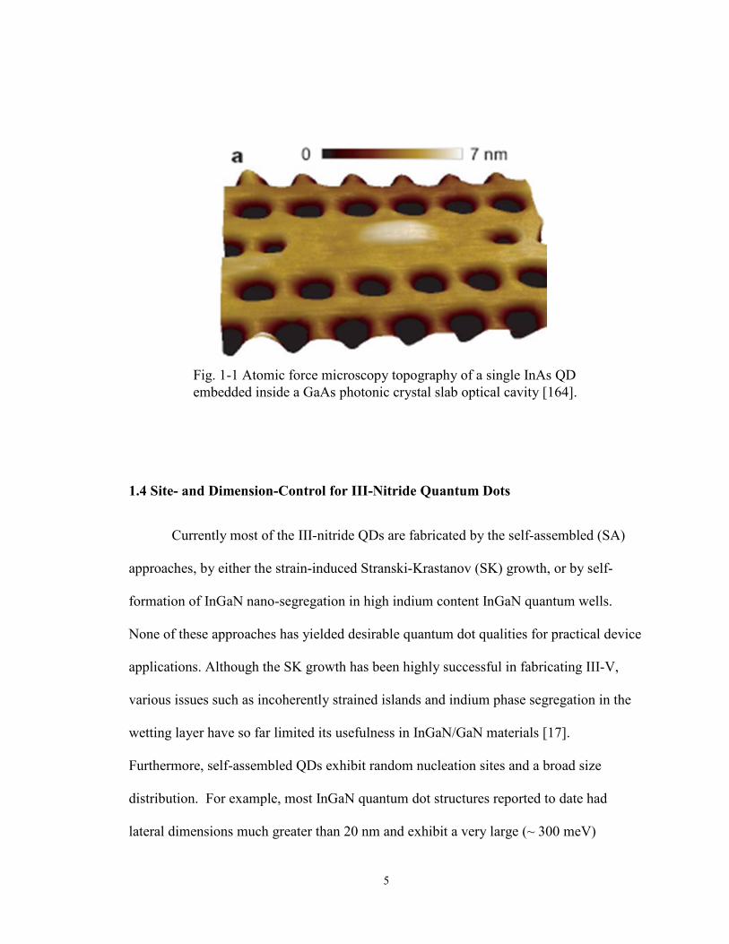
semiconductor quantum light sources. Figure 1-1 Shows the such system with an InAs
QD placed at the center (defect) of a photonic crystal slab cavity; strong coupling and
single-photon emission were observed at 4.2 K [164].
5
1.4 Site- and Dimension-Control for III-Nitride Quantum Dots
Currently most of the III-nitride QDs are fabricated by the self-assembled (SA)
approaches, by either the strain-induced Stranski-Krastanov (SK) growth, or by self-
formation of InGaN nano-segregation in high indium content InGaN quantum wells.
None of these approaches has yielded desirable quantum dot qualities for practical device
applications. Although the SK growth has been highly successful in fabricating III-V,
various issues such as incoherently strained islands and indium phase segregation in the
wetting layer have so far limited its usefulness in InGaN/GaN materials [17].
Furthermore, self-assembled QDs exhibit random nucleation sites and a broad size
distribution. For example, most InGaN quantum dot structures reported to date had
lateral dimensions much greater than 20 nm and exhibit a very large (~ 300 meV)
Fig. 1-1 Atomic force microscopy topography of a single InAs QD embedded inside a GaAs photonic crystal slab optical cavity [164].

6
inhomogeneously broadened linewidth [15]. A summary of these self-assembled InGaN
quantum dot structures is given in Table 1-1. Figure. 1-2 is the graphical interpretation of
Table 1-1.
As mentioned in Section 1.3, many of the advanced application of QDs, such as
QD-cavity quantum light sources, require the addressability of a single QD. The self-
assembled approaches for QDs, which produce QDs with random location (and
dimension), of course, fail to meet this requirement. For example, to perform a QD-cavity
integration, most (almost all) of the authors in the reported literature have gone a long
way to first locate and isolate a single QD from a self-assembled, sparsely congregation
of QDs, by means of scanning electron and/or atomic force microscopy, and then to build
the optical cavity around that single QD. This resources-exhausting process for locating a
single QD is one of the major obstacles that hinder the practical use semiconductor QD-
cavity quantum light source.

7
Growth & Structure X = Indium (In) composition
Dimension
D = Average dot diameter Z = Average dot height
Dot Density Remarks Reference
MOCVD Antisurfactant (Si) X = 0.25 – 0.38 GaN(5nm)/ InxGa1-xN/ Al0.24Ga0.76N (300nm)/ Al0.12Ga0.88N (100nm)
D = 10nm Z = 5 nm
1E10 – 1E11 cm-2 [23]
MOCVD SK growth InGaN(6.4-19.1ML)/GaN
D = 9-16 nm Z = 4.5-5.4 nm
1E10-2E10 cm-2 [24]
MOCVD SK growth 10 period In0.2Ga0.8N QD/In0.02Ga0.98N(5nm) laser structure
D = 19.5 nm Z= 4.5 nm
6E9 cm-2 [25]
MOCVD SK growth X = 0.2 – 0.4 In0.02Ga0.98N(20nm)/ InxGa1-
xN(12.5ML)/GaN(1.1um)
D = 23.4 nm Z = 4.6 nm 1E10 cm-2 [26]
LP-MOCVD In segregation(fluctuation) / In-rich domains GaN(20nm)/ InxGa1-
xN/GaN/Al0.05Ga0.95N/AlN(1.1um)
D ~ 5 nm [27]
LP-MOCVD In segregation(fluctuation) / In-rich domains X = 0.18-0.23 GaN(100nm)/ InxGa1-x MQW/GaN(2um)
D = 3-5 nm 1E11-1E12 cm-2 [28]
LP-MOCVD SK, Interruption InxGa1-x (2.4nm)/GaN(2um)
D = 20-35 nm Z = 4 nm 2E10 cm-2
Growth interruption technique. Annealing is part of the experiment.
[29]
MOCVD Silane treatment GaN(10nm)/ InxGa1-x QD in 8 period/Si:GaN(2um)
D ~ 15 nm Z = 3.6-4.1 nm 2.1E11-2.9E11 cm-2
Silane treatment; roughened SiNx layer deposition before QD growth
[30]
MOCVD Antisurfactant (In) GaN(20nm)/GaN(5nm)/ In0.01Ga0.99N(4nm)/In treatment QD/In0.01Ga0.99N(4nm)/GaN(2um)
D = 4 nm Z = 1.5 nm
In was used as anti-surfactant [31]

8
Growth & Structure X = Indium (In) composition
Dimension
D = Average dot diameter Z = Average dot height
Dot Density Remarks Reference
MOCVD Post-growth N2 anneal GaN(7nm)/InGaN(10ML)/GaN(2.8um)
Z = 1 nm 1E10 cm-2 Post-growth N2 anneal [32]
MOCVD SK and growth interruption GaN(20nm)/InGaN QD/GaN(10nm)/GaN(1um)/AlN(500nm)
D = 20 nm Z = 1.5 nm 9E10 cm-2
SK and growth interruption
[33]
MBE SK Growth 12 period In0.3Ga0.7N QD/GaN(15nm)/GaN(2um)
D = 27 nm Z = 2.9 nm 9E10 cm-2 [34]
MBE SK Growth X = 0.15 In0.15Ga0.85N QD/GaN(few microns)
D = 35 nm Z = 4 nm 5E10 cm-2 [35]
MOCVD SK Growth X = 0.45 5 period GaN(20nm)/InGaN QD/GaN(2um)
D = 46 – 78 nm Z = 1.32 – 2.81 nm 1.6E9 – 8.8E9 cm-2 [36]
MOCVD X = 0.23-0.3 SK and growth interruption GaN(20nm)/InGaN QD/GaN(10nm)/GaN(1um)/AlN(500nm)
D = 20 - 50 nm Z = 2.8 - 8 nm 1E10 – 9E10 cm-2 [37]
MBE X = 0.15 SK Growth InGaN QD/GaN(3um)
D = 15 nm Z = 2 nm 1E11 cm-2 [38]
MOCVD X ~ 0.35 SK Growth InGaN + N2 anneal QD/GaN(3um)
D = 40 nm Z = 4 nm InGaN layer
+ N2 anneal [39]
LP-MOCVD SK Growth, Interruption InGaN QD LED
D = 20 -35 nm Z = 4 nm SK,
interruption [40]
Table 1-1 A summary of size and density of self-assembled InGaN QDs reported in the literature.

9
The absence of site-control is not the only concern for SA QDs. There is no
control over the dimension of the SA QDs either. This somehow raises the doubt of the
quantum nature of SA QDs because the dimension of the QD core determines the level of
quantum confinement. A characteristic length, called the de Broglie wavelength, can be
used to evaluate the level of quantum confinement based on the dimension of a QD (or in
general, a potential trap). For a particle (e.g. electron) having mass meff and is confined
one-dimensionally to a length Δx, the de Broglie wavelength, its uncertainty in
momentum is ∆p ≈ ħ / ∆x, corresponding to the an uncertainty in energy ∆E ≈ ħ2 /
2(meff)(∆x)2, where ħ is the Planck’s constant. This uncertainty in energy represents the
0 10 20 30 40 500
2
4
6
8
10
Qua
ntum
Dot
Den
sity
(101
0 cm
-2)
Quantum Dot Diameter (nm)Fig. 1-2 Graphical interpretation of the reported dot sizes and densities listed in Table 1-1.
Electron de Broglie wavelength in InGaN (~ 27.3 nm at 6 K, ~ 6 nm at 150 K, ~ 3.9 nm at room-temperature)

10
separation of quantized energy levels when the particle is confined. Therefore, de Broglie
wavelength Δx is the confinement dimension that gives energy quantization ∆E. At
temperature T, the particle possesses thermal kinetic energy (1/2)kBT, corresponding to a
∆x ≈ ħ / [(meff)(kB)T]1/2, where kB is the Boltzmann constant. For the size quantization
effect to be significant, the particle must see a ∆E greater than its thermal energy
(otherwise it will have equal probability to occupy both energy levels), and therefore the
physical length of confinement, L, must be smaller than de Broglie wavelength at that
temperature. Going back to Fig. 1-2, there are dashed lines represent the electron de
Broglie wavelengths of III-nitride materials (InGaN) at different temperatures; it can be
seen that most of the SK InGaN QDs are larger than the electron de Broglie wavelength
at room temperature, raising doubts on their quantum nature at that temperature.
Rigorously speaking, these “quantum dots” only exhibited quasi-0D confinement because
of the small (~3.86 nm at room-temperature) electron de Broglie wavelength in III-nitride
materials [16]. The temperature of 150 K has its technological significance: this is the
temperature that can be achieved by on-chip thermoelectric coolers; it means that for a
practical, monolithically-integrated device that uses QD, such as a quantum light source,
the QD in question should have diameter less than 6 nm.
As an example we use the information provided by Ref. 69 to estimate the
dimension required for InGaN quantum dots; we note that the transverse (vertical)
dimensions can be very small because they are controlled by epitaxy. The required lateral
dimension ||L can be estimated by an infinite barrier model in which the energy
separation between the first two sub-bands is given by

11
=− 2
||
22
123
*2 LmEE π
where m* is the effective mass of the carriers in the dot region. The typical InGaN
quantum dot has an estimated homogeneous linewidth of 10 meV at room temperature
extrapolated from the micro-PL data reported in Ref. 69. To observe the delta-function
like density of states, Ec2 - Ec1 must be at least 10 meV. This imposes an upper limit on
||L to be 7 nm (using 0mmhh ≈∗ ).
Therefore, in order to obtain a fundamental understanding of the optical and
electronic properties of III-nitride quantum dots, and to utilize them in practical
applications, it is crucial to obtain “small”, site-controlled and high-quality quantum dots.
1.5 Objective of this Thesis
Based on our discussion of III-nitride QDs above, we have set the long-term goal
of this research project - to create a semiconductor single-QD-cavity quantum light
source (e.g. single-photon source) that can operate at room temperature, and can be
readily incorporated into the current mass-production scheme. This goal can be broken
down into four objectives: site- and dimensional control of individual III-nitride QD, the
making of III-nitride optical cavity, the development of nanometer-scale pattern-transfer
technique and the development of high-throughput nanopatterning. This thesis will report
our establishment in these four objectives as we progress towards our goal.

12
As one may already see, among the objectives, the site- and dimension-control of
the III-nitride QD is the most critical one, because the dot dimension determines the
operation of the QD (quantum confinement, emission energy, operating temperature; see
Section 1.4), and the dot site determines the QD’s integration on the device level. The
first and the most crucial objective of this research, is therefore, to fabricate and
characterize high quality III-nitride quantum dots with controlled locations, dimensions,
geometry, and chemical composition. Because most of the issues associated with the
current III-nitride quantum dot fabrication stem from the 2D to 3D transition in the SK
growth, one expects to avoid these issues by eliminating this transition. Moreover, many
of the advanced applications of QD such as single-photon emission, emission in the
strong-coupling regime and single-atom lasing, require the addressability of a single QD
inside an optical cavity [1,2,3,4,164,165], and are severely demotivated by QDs formed
by the SK growth with randomly distributed size and location. By introducing the site-
and dimension-control to the QDs, we expect to avoid the short-coming of locating
individual SA QDs dots, and to improve upon the device integration level, especially for
single-dot devices.
In this research, we propose to apply both selective area epitaxy (SAE) and the
top-down etching approach to achieve an unprecedented control of the III-nitride
quantum dots that will be suitable for a wide range of device applications. Selective area
epitaxy has been successful in making III-V quantum dot lasers [18,19] and a variety of
GaN based nanostructures including nanowires [20] and nanodots [21,22]. However, the
lateral dimensions of state-of-the-art SAE-grown nanostructures were still be around 50
nm or larger. To achieve high quality III-nitride quantum dots using SAE, the lateral

13
dimensions must be reduced by an order of magnitude from the current status quo. New
patterning techniques and a fundamental understanding of the growth profile evolution
during nanoscale SAE are required to reach this goal. Top-down approach refers to the
formation 3D nanostructures by selectively etching down into a planar surface. Top-down
etching approach has been successfully used to make III-nitride nanostructures including
nanodots [74,75,76,77,78]. However, the dot’s diameters are often larger than 50 nm and
the etched nanostructures (nanopillars or nanoposts) from MQWs do not represent the
realistic structure of a single QD. The capability of making site-controlled III-nitride QDs
using the top-down approach has been overlooked. This work will explore and
characterize high-quality, site- and dimension-controlled III-nitride QDs implemented by
both SAE and the top-down approach.
This thesis is organized as follows. In Chapter 2, basic principles are described for
producing site- and dimension-controlled III-nitride epitaxial structures using SAE. A
simple empirical model is developed to simulate the geometry of micro- and nano-scale
III-nitride structures grown by SAE. We also demonstrate the fabrication of site- and
dimension-controlled InGaN quantum dots using SAE. A phase-field model developed
by our collaborator is used to describe and to predict the morphology evolution of a
nanodot during SAE. In Chapter 3, we present the fabrication of site- and dimension-
controlled InGaN QDs by etching down a patterned InGaN single quantum well. In
Chapter 4, optical properties of the site- and dimension-controlled InGaN QDs are
characterized. Experimental results are analyzed and discussed. In Chapter 5, we
demonstrate bandgap-selective photo-electro-chemical etching of III-nitride materials,
which can be adopted to make suspended III-nitride optical cavities incorporating a single

14
InGaN quantum dot. In Chapter 6, we propose two patterning techniques, pattern
shrinkage by spacer and by electrodeposition, with the former aiming at nanometer-scale
patterned features and the latter aiming at the large-scale nanofabrication. These
techniques can be applied to the site-controlled quantum dots as developed in this thesis
for scalable, large-area fabrication. In Chapter 7, we will summarize and make
suggestions for future work.

15
Chapter 2
Selective Area Epitaxy for III-Nitride Nanostructures
The two most common approaches for enforcing control over epi-structures, namely
the selective area epitaxy (SAE) and the top-down etching, rely on lithography and the
subsequent pattern-transfer processes. SAE refers to the application of epitaxy to a
substrate pre-patterned with a growth mask, on which no nucleation can occur; epi-
structures are restricted to exist only within the openings on the growth mask; by
patterning of the growth mask openings, site and dimension-control of the epi-structures
can be achieved. In the chapter, we will use SAE to fabricate the site- and dimension-
controlled InGaN QD heterostructures. Compared to the straight-forward top-down
approach, SAE will see another level of sophistication, due to the fact that growth
mechanism of SAE results in localized and pattern-dependent growth rate. The SAE-
grown epi-structures will also have 3-D growth profiles dominated by the slowest-
growing crystal facet, a phenomenon called growth rate anisotropy. These features of
SAE can be leveraged for different applications, such as to reduce defect density by

16
lateral overgrowth, to form templates for semipolar quantum well (QW) growth, and to
produce epi-structures with graded properties e.g. dimension, composition and/or
emission wavelengths, in a single epitaxial run. In the following, we will present the
basic principles and the overviews of SAE. We will demonstrate the use of SAE in nano-
scale to fabricate III-nitride site- and dimension-controlled nanostructures. The
combinational effect of pattern-dependent growth rate, the growth rate anisotropy and the
coalescence of crystal facets result in the evolution of 3-D morphology of the
nanostructures during SAE. This nanoscale morphology evolution was studied
experimentally and the results agreed qualitatively with that from the theoretical
simulation using the phase-field model.
2.1 Selective Area Epitaxy for III-Nitride Materials
2.1.1 Overview
The use of patterned masking layers to spatially define epitaxial growth is commonly
known as the selective area epitaxy (SAE) or selective area growth (SAG)
[41,43,44,45,46,49]. SAE is typically accomplished by making openings on a masking
layer, followed by an epitaxial growth. The masking layer is usually a layer of amorphous
dielectric (e.g. silicon dioxide) [45,48] or metallic (e.g. tungsten) materials [42] deposited
on top of an epitaxial surface. Due to the difference of surface kinetic energy, growth
species will prefer to nucleate and grow on a crystalline, epitaxial surface instead of the
amorphous, masked surface, thus creating the selectivity of crystal growth over the two
different surfaces. Therefore SAE allows one to precisely control the positions and

17
dimensions of epitaxial micro- and nanostructures, by controlling the shape and site of
the mask openings. Figure 2-1 shows III-nitride epi-structures formed by SAE, with
dimensions ranging across 3 orders of magnitude in length-scale, from tens of microns
(optical lithography) to tens of nanometers (e-beam lithography) [58].
In III-nitride semiconductors, SAE has been widely used to reduce the threading
dislocation density [41,42]. For this purpose, some features of SAE are intentionally
leveraged to perform an epitaxial procedure called the epitaxial lateral overgrowth
(ELOG). Unlike thin film growth, SAE enables additional crystal facets to be formed,
thereby allowing one to control the resulting micro- and nano-structural geometry via
different growth conditions including growth temperature and reactor pressure. For
example in the ELOG process, the lateral growth of vertical facets is intentionally
enhanced to terminate the TDs. This phenomenon can be further enhanced by the
diffusion of source species over the amorphous surface towards the epitaxial openings,
resulting in an enhanced growth rate at the selected region. Indeed, the modulation of
Fig. 2-1 Scanning electron micrographs (SEMs) of epi-structures formed by SAE. Different lithographic tools (contact aligners, stepper and e-beam lithography) were used to pattern openings across the length-scale on the masking layer.

18
local growth rate via different mask patterns has been successfully applied to the
monolithic integration of III-V photonic devices.
In this chapter, we have applied one of the proposed lithography-based techniques,
the SAE, to the fabricate site- and dimension-controlled III-nitride quantum dots. As
mentioned in the Introduction, III-nitride quantum dots grown by the Stranski-Krastanov
(SK) method require the deposition of a thin wetting layer, considerably limiting the
quality and size of the resulting strain-induced quantum dot structures. Using SAE, the
quantum dot growth is similar to the thin-film growth and is expected to have the
following advantages:
1. No wetting layer with a large mismatch is required. This is expected to greatly
improve the quality of the III-nitride quantum dots.
2. The dimensions of the quantum dots are solely determined by the lithographic
patterning, rather than by the strain. This is expected to allow on to obtain sub-
10nm InGaN quantum dots that have been difficult to achieve using the SK
growth mode.
3. The positions of the quantum dots are precisely defined, allowing one to easily
integrate these quantum dots with other optoelectronic components, such as
optical cavities.
4. Because the growth of the quantum dots is not strain induced, compressively
strained (e.g. InGaN on AlGaN), unstrained (e.g. InGaN on AlInN), and tensile
strained (e.g. GaN on AlInN) quantum dots are all possible.

19
In Section 2.1.2, we will describe an empirical model to control the size and
geometry of the III-nitride micro- and nano-structures using SAE. This is critical in
controlling both the optical and electronic properties of the III-nitride quantum dots.
Later in Sections 2.3 – 2.6, we will demonstrate the feasibility of using SAE to achieve
site- and dimension-controlled III-nitride nanostructures. Morphology evolution of the
nanostructures due to the growth mechanism and growth rate anisotropy of SAE will be
studied in details.
2.1.2 Modeling of Selective Area Epitaxy for Micro- and Nano-Structure Growth
There are two fundamental differences between selective area epitaxy and planar
thin film growth. The first difference is the incorporation of growth selectivity through
use of masking layer during epitaxy; the second being the supply mechanism of growth
species to the epitaxial surfaces. During SAE, source species will impinge on both the
mask and the epitaxial surfaces, simultaneously causing nucleation on the mask and on
the exposed epitaxial surface. On the mask, roughness and impurities will create irregular
nuclei causing the heterogeneous nucleation which leads to the formation and growth of
polycrystals on the mask [46]. In general, selectivity of SAE is determined by the amount
of polycrystal deposition on the mask. High selectivity is achieved when the
supersaturation of growth species on the mask is sufficiently low to prevent the
heterogeneous nucleation, while the nucleation barrier on the exposed epitaxial surface is
extremely low in comparison [45]. Selectivity can be affected by the growth condition,
the mask materials and the reaction chemistry (of the source species) [43,44,45,46,47,48].

20
Intuitively, polycrystal deposition can be inhibited by decreasing the reactor pressure and
increasing the growth temperature, which, respectively, reduces the flux of growth
species impinging on the sample surface and shortens the residence time of species
migrating on the mask [44,45,47,48]. Fortunately, these two conditions are already
fulfilled in most of the modern systems of chemical vapor deposition (CVD) adopting
metalorganic sources [44,45]. Excellent selectivity has been demonstrated using these
metalorganic CVD (MOCVD) systems. In this research, we use a Thomas-Swan close-
coupled-showerhead (CCS) MOCVD system for all the epitaxial growth.
SAE in MOCVD is performed in vapor phase, in which the growth species are
delivered, in the form of vapors, to the epitaxial surface where they react due to the high
growth temperature to nucleate and grow. Different from the two-dimensional thin film
growth in which the growth species are uniformly delivered to the epitaxial surface, SAE
in the same vapor phase environment will have two supply mechanisms of the growth
species: the vapor-phase diffusion and the surface diffusion [47,48,49] (Fig. 2-2). The
vapor-phase diffusion refers to the lateral diffusion of source species due to concentration
gradient in the stagnant layer, which occurs in the vicinity above the mask opening, as a
result of growth-initiated source depletion; surface diffusion refers to the migration of the
source species on the mask until they reach the mask openings. Both mechanisms are
equally important to determine the growth process in the openings. Their dominance of
the growth can be the differentiated by the dimension of the mask surrounding the
openings [47,48,49]. If the mask dimension is comparable to the surface diffusion length
of source species Ls on the mask, vapor-phase diffusion will dominate the growth process.
On the other hand, if the mask dimension is much smaller than Ls, surface diffusion will

21
dominate the growth. Intuitively, this weighing of dominance can be thought as the
desorption of source migrating on the mask surface into the vapor-phase before it has a
chance to reach the mask openings, thus subduing the factor of surface diffusion in the
growth within the openings. Surface diffusion as a lateral supply mechanism for the
source generates an extra supply of growth species near the edge of the openings,
resulting in a non-uniform “tail” or “ring” profile in the openings [21,22,47]. Moreover, if
surface diffusion dominates, growth species will tend to migrate on the mask surface
before they nucleate in the opening. This means that any impurities or roughness on the
mask, which themselves act as irregular nuclei who gather migrating species passing
within the Ls around them, can potentially affect the growth in the openings. This raises
the requirement for mask cleanliness in SAE [46]. In general, surface diffusion is seen as
a deleterious effect in SAE.
The profile, or geometry, of the crystalline structures formed within the openings
is a sophisticated compilation of many process parameters. It is known that during the
Fig. 2-2 Source supply mechanisms during selective area epitaxy.
1. Precursor adsorption 2. Surface diffusion 3. Desorption or nucleation 4. Desorption or polycrystal

22
SAE, the growth profile evolves with time and is known to be significantly affected by
factors including the dimension [47,48,49] and orientation [53,54] of mask openings,
mask materials [48] and growth conditions [52]. The variation of the growth profile in
turn will produce different material compositions and optical properties of the resulting
structures [55,56,59]. In general, it is thought that the edge of the mask contacting the
epitaxial surface enforces the incorporation of source atoms into certain low-energy
atomic configurations, which are usually manifested as the crystal facets, through the
blocking of certain dangling bonds [41,52] and/or the variation of surface contact angle
[51]. The crystal facets then evolve following the growth rate anisotropy [50], which is
the growth rate dependence on the crystal orientation (Fig. 2-3). Usually, faster-growing
facets propagate, coalesce and cancel out each other, leaving behind the slow-growing
crystal facets to dominate the final geometry of the epitaxial material formed within the
openings. The facet formation and growth rate anisotropy are, of course, functions of
growth conditions [52,53,54]. Fortunately, under typical growth conditions, the growth
profiles are predictable as they are dominated by the slowest-growing (the most stable)
facets [52,56]. For SAE in III-nitride MOCVD, the {1 1 01} facets seem to be the most
stable under typical growth conditions therefore they dominates the SAE structures
[52,56].

23
To model the growth profile evolution is a difficult task because the subject needs
to take into account the diffusion processes (in vapor-phase on mask surface) of the
source species and dynamic process of facet formation, while the two processes exist in
different length scales – the diffusion processes are macroscopic phenomena which
involve a large number of atoms over a large volume (usually over hundreds of cubic
micron), while the facet formation deals with the dynamics of nucleating individual
atoms, which is in nanometer-scale. Models based on one process usually neglects the
other. To date, the level-set method [60,61] exists as one of the better models to describe
growth profile evolution by simultaneously considering the thermodynamics of growth,
the diffusion processes, and the associated growth rate anisotropy [62,63].
Since the geometrical profile of SAE-formed III-nitride materials significantly
affects their optical properties [55,56,59], it is important to study the evolution of the
growth profile during SAE. To have a better understanding of the geometry of epitaxial
structures formed by SAE, we developed a relatively simple model to track the growth
Fig. 2-3 Growth rate anisotropy of different crystal planes during selective area epitaxy using MOCVD [35,46].
T

24
profile evolution. The model assumes different propagation velocities for facets of
different orientations, and uses this to simulate the effect of growth rate anisotropy. The
model is described in Fig 2-4 .The initial two-dimensional growth profile of the dot is
extrapolated by a series of “markers”. The markers are connected by “facets” between
them, whose fronts propagate according to growth rate anisotropy data entered
empirically for that facet. The growth rate or the propagation velocity of each crystal
facet is assigned according to its orientation, which can be interpreted as the angle the
facet intersecting the horizontal z-plane. Positions of the markers after certain time
interval t∆ can then be calculated from the following simple equations:
21
1200'
mmhhxxxx
−−
+=∆+= (Eqn. 2-1)
2 1 1 20 0
2 1
' m h m hz z z zm m
−= + ∆ = +
− (Eqn. 2-2)
( )( ) )2(1)2(1)2(1)2(1)2(1 coscos θθθ tRdh ∆⋅== (Eqn. 2-3)
where ( )θR is the growth rate anisotropy value as a function of the angle between the
facet normal and the z-plane. An example of ( )θR , which can be incorporated in the
program as empirical data, is shown in Fig. 2-5. This ( )θR is constructed based on the
growth rate anisotropy observed experimentally in Ref. 41 and Ref. 52. The coalescence
of the facets is interpreted in the model as the interchange of positions between two
neighboring markers. When this happens, the point that has higher y value will stay and
represent the surviving facet formed after coalescence, while the other marker will be

25
eliminated from the profile because the facet it represents is “grown over” during
coalescence.
Fig. 2-5 The plot of ( )θR entered as empirical data.
0 20 40 60 80
2
4
6
Grow
th R
ate
(Ang
stro
m /
sec)
Plane Normal Angle (degree)
MarkersMarkers
After Δt
Fig. 2-4 A simple model to trace the evolution of crystal facets taking into consideration the effect of growth rate anisotropy.
X
Z

26
The coalescence of crystal facets can be shown in Fig. 2-6. Initially, there is a pit
(or a trench) consisting of 45º-tilted crystal facets as its sidewalls, residing at the center of
z-plane facet of a crystal. The growth rate anisotropy ( )θR is entered deliberately such
that the growth rate of the top crystal facet, the top z-plane, is slower than that of the 45º-
tilted facets, as shown in Fig. 2-7. ( )θR is deliberately set simply to make the tilted facets
grow faster, for the verification of any possible coalescence that would occur in the pit. In
this situation, one should expect to see that that the majority of the slow-growing planes
remain after an extended amount of growth time. This has been verified in the model as
the sidewalls of the pit propagate and coalesce, filling the pit and leaving only the slow-
growing z-plane facet in the end (Fig. 2-6).
50 100 150 200 2500
50
100
150
200
Y (n
m)
X (nm)
Fig. 2-6 A trench or a pit with 45° sidewall on the z-plane of a crystal. Growth rate anisotropy makes the inclined facets grow faster and coalesce, filling the void. Only the slower-growing z-plane remains after extended amount of growth time.

27
2.2 Prior Work of III-nitride Nanostructures using Selective Area Epitaxy
Chen et. al. demonstrated the use of SAE to accurately define the site and
dimension (lateral dimension) of InGaN/GaN nanodots [21,22]. In their approach, the
nanoscale openings on the SiO2 mask layer are made by e-beam lithography followed by
reactive ion etching. The smallest dot size after SAE was still greater than 50 nm. In a
study conducted by Hersee et al., high quality GaN nanowires were grown in hole
Fig. 2-7 Exaggerated facet-angle-dependent growth rate used in the simulation shown in Fig. 2-6. Facets with angle greater than 70° are assigned a slower growth rate compared to the less-tilted facets; because of this, slowest growing facets/planes dominate the final profile as the tilted facets coalesce, demonstrating and validating the effect of growth rate anisotropy using the simple point-tracking model.
0 10 20 30 40 50 60 70 80 900
2
4
6
Grow
th R
ate
(Ang
stro
m /
sec)
Plane Normal Angle (degree)

28
openings patterned on a SiN mask [20]. Average diameter of the wires is about 200 nm.
In these work, the dimensions of the nanostructures are too large to generate clear
quantization effect at high temperature. Therefore to fabricate site-controlled III-nitride
quantum dots using SAE, we attempt to make the nanoholes on the SAE mask as small as
possible so as to limit the lateral dimension of the nanodots grown within. Ideally, one
has to develop a reliable sub-10 nm patterning technique to satisfy the dimensional limit
of site-controlled quantum dots (Section 1.2). Later in Chapter 6, we will address the
issues regarding the resolution and throughput of the patterning techniques.
For SAE, in addition to the requirement of patterning quality, it is also important
to understand and to control the dimension and shape of each epitaxial layer because the
optical properties of the as-resulted III-nitride nanostructures are very sensitive to their
dimensions and shapes due to the large and anisotropic piezoelectric fields
[55,56,59,87,88,89]. In previous reports, structural and optical properties have been
characterized for these nanostructures, but a detailed study of the growth profile
evolution in nanoscale SAE (NSAE) is still lacking. Here we present a more detailed
study of the growth profile evolution of NSAE, by combining both the theoretical model
and experimental observation. Conclusions obtained from the profile evolution study can
elucidate certain aspects of optical properties we observed in SAE InGaN nanodots.
2.3 General Patterning Technique for the Nanoscale SAE
As mentioned in Section 2.1, SAE requires openings in a layer of dielectric mask
(SiO2, Si3N4, Al2O3 etc.) to expose the crystalline surface where epitaxy can occur. For
29
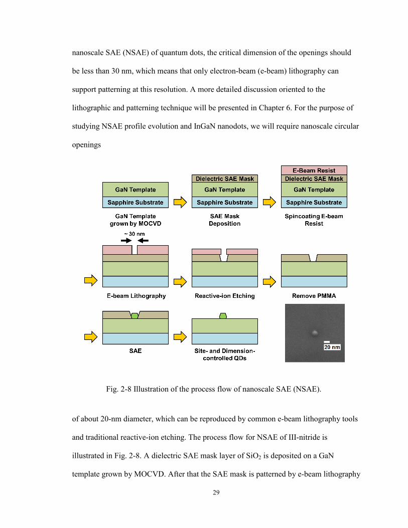
nanoscale SAE (NSAE) of quantum dots, the critical dimension of the openings should
be less than 30 nm, which means that only electron-beam (e-beam) lithography can
support patterning at this resolution. A more detailed discussion oriented to the
lithographic and patterning technique will be presented in Chapter 6. For the purpose of
studying NSAE profile evolution and InGaN nanodots, we will require nanoscale circular
openings
of about 20-nm diameter, which can be reproduced by common e-beam lithography tools
and traditional reactive-ion etching. The process flow for NSAE of III-nitride is
illustrated in Fig. 2-8. A dielectric SAE mask layer of SiO2 is deposited on a GaN
template grown by MOCVD. After that the SAE mask is patterned by e-beam lithography
Fig. 2-8 Illustration of the process flow of nanoscale SAE (NSAE).

30
which makes nanoscale openings on the e-beam resist. The e-beam resist is directly used
as an etch mask in the subsequent reactive-ion etching (RIE) in which the nanoscale
openings are pattern-transferred to the SAE mask layer. The patterned sample is then
transferred back to the MOCVD for SAE.
Common e-beam lithography systems together with reactive-ion etching can
reliably achieve isolated dot openings with diameter greater than 30 nm. To achieve sub-
30 nm dot patterning on dielectric materials, the process, however, requires fine-tuning of
the processing conditions and is often sensitive to the status of the tools. Nevertheless, by
fine-tuning the RIE condition, the etch bias can be reduced so that the resulting aperture
enlargement after EBL can be minimized. Figure 2-9 shows the effects of different
etching chemistries on the size of the openings. One condition results in an opening
diameter of about 20 nm and the other about 30 nm. It is thought that the reduction of
argon (Ar) flow reduces the sputtering and hence enhances the passivation of sidewalls
during RIE, which inhibits the undercut (etch bias) due to the chemical component of the
etching. In the following, we study NSAE profile evolution and InGaN nanodots using
patterned mask with 25-nm-diameter openings, of which we can reliably reproduce
utilizing the readily available nanofabrication capabilities.

31
The sample preparation is described as follows. First, a 1.5-μm thick GaN
template was epitaxially grown on a c-plane sapphire substrate at 1050 ºC with a 25 nm
low-temperature nucleation layer. A 40 nm thick SiO2 layer was then ex situ deposited by
plasma-enhanced chemical vapor deposition. The SiO2 layer was patterned into an array
of 900 by 900 nanoscale holes for the subsequent SAE using electron-beam lithography
(Raith 150 with PMMA resist) and reactive ion etching (Oxford Instruments
PlasmaTherm 790). The hole diameter was measured to be 25 nm (Fig. 2-10 inset). The
spacing between two adjacent nanoholes was fixed at 100 nm, giving an array density of
1010 cm-2. After the removal of the PMMA resist by acetone and oxygen plasma ashing,
the sample was transferred to a Thomas-Swan closed-coupled showerhead MOCVD
system for SAE. The sample was ramped up to 760 ºC and was deposited with a GaN
layer of a nominal thickness 40 nm. The evolution of morphology was recorded by
interrupting SAE at different times. Figure 2-10 shows the scanning electron micrograph
Fig. 2-9 (a) Dot openings on SiO2 mask using Ar flow of 15 sccm in RIE. (b) Dot openings on SiO2 mask using Ar flow of 5 sccm in RIE.
(a)
(b)
30 nm 21 nm

32
(SEM; Nova Nanolab) of a typical GaN nanodot array after the deposition of 40-nm-thick
GaN during SAE. The base diameter distribution of the nanodot array has a mean of
51.73 nm with a standard deviation of 2.9 nm.
2.4 Phase-Field Model and Growth Morphology Evolution
To investigate the evolution of growth morphology, the SAE was interrupted at
different times and the as-grown samples were imaged as shown in Fig. 2-11. It is known
that during SAE, the growth profile evolves with time and is known to be significantly
affected by factors including the dimension [47,56] and orientation [53,54] of the mask
openings, mask materials [48] and growth conditions [20,41,52]. The variation of the
Fig. 2-10 SEM image of GaN nanodot array grown by SAE. The image was taken after the removal of the SiO2 SAE mask. The inset shows nanoholes in SiO2 with diameter of 25 nm after patterning.

33
growth profile in turn will produce different material compositions and optical properties
of the resulting structures [55,56,59,87]. During SAE, the primary supply of growth
species to nanodots occurs through vapor-phase diffusion. In addition to direct deposition
from the vapor phase, deposition occurs onto the mask, resulting in adatoms that can be
incorporated through surface diffusion or vapor-phase diffusion (after re-evaporation),
which can enhance deposition at the edge of the nanodot [47]. This additional flux results
in a localized growth rate enhancement (Stage I, Fig. 2-11). Nanoring structures are
observed in this stage [21,22]. As growth proceeded, the effect of growth rate anisotropy
started to coalesce different crystal planes around the edge towards the center of the
nanoring (Stage II, Fig. 2-11). Eventually, the slowest growing plane dominated the
growth profile, resulting in a hexagonal pyramidal shape (Stage III, Fig. 2-11).

34
The study of growth profile evolution is collaborated with Dr. Larry Aagesen in
Prof. Katsuyo Thornton’s research group. Growth profile evolution during NSAE is
simulated by the phase-field method, where the value of an order parameter φ delineates
the film and vapor. The order parameter evolves via the Cahn-Hilliard equation, modified
Fig. 2-11 The left column shows the SEM images taken at the different stages of the nanoscale SAE and the right shows the calculated morphology. The scale bars on the left and on the right are 50 and 40 nm, respectively.
35
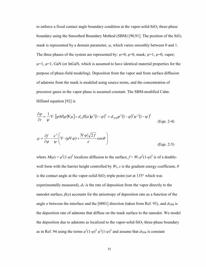
to enforce a fixed contact angle boundary condition at the vapor-solid-SiO2 three-phase
boundary using the Smoothed Boundary Method (SBM) [90,91]. The position of the SiO2
mask is represented by a domain parameter, ψ, which varies smoothly between 0 and 1.
The three phases of the system are represented by: ψ=0, φ=0, mask; ψ=1, φ=0, vapor;
ψ=1, φ=1, GaN (or InGaN, which is assumed to have identical material properties for the
purpose of phase-field modeling). Deposition from the vapor and from surface diffusion
of adatoms from the mask is modeled using source terms, and the concentration of
precursor gases in the vapor phase is assumed constant. The SBM-modified Cahn-
Hilliard equation [92] is
( )[ ] ( ) ( ) ( ) ( )222222 1111 ψψϕϕϕϕαβµϕψψ
ϕ−−+−+∇⋅∇=
∂∂
TPBV ddMt (Eqn. 2-4)
∇+∇⋅∇−
∂∂
= θε
ψϕψ
ψε
ϕµ cos
2)(
2 ff
(Eqn. 2-5)
where M(φ) = φ2(1-φ)2 localizes diffusion to the surface, f = Wf φ2(1-φ)2 is of a double-
well form with the barrier height controlled by Wf, ε is the gradient energy coefficient, θ
is the contact angle at the vapor-solid-SiO2 triple point (set at 135° which was
experimentally measured), dV is the rate of deposition from the vapor directly to the
nanodot surface, β(α) accounts for the anisotropy of deposition rate as a function of the
angle α between the interface and the [0001] direction (taken from Ref. 93), and dTPB is
the deposition rate of adatoms that diffuse on the mask surface to the nanodot. We model
the deposition due to adatoms as localized to the vapor-solid-SiO2 three-phase boundary
as in Ref. 94 using the terms φ2(1-φ)2 ψ2(1-ψ)2 and assume that dTPB is constant

36
throughout the deposition process because the distance between nanodot edges changes
very little during these early stages of deposition (we ignore the transient during the very
early phase). We used ε=1, Wf,=1, a grid size of 300 x 300, grid spacing Δx=1, and time
step Δt =2.0, and varied dV and dTPB. The results exhibit a good agreement with the
experimental observations as shown in Fig. 2 using dV=0.00093 and dTPB=0.33,
reproducing the volcano-like shape in the early stage and predicting an emergence of the
facets with slow growth at the later stage of the deposition process. Such transitions were
not observed unless the deposition onto the mask was accounted for, and were only
reproducible within a small range of the parameter sets. In particular, we found that the
dewetting contact angle and the specific values of dV and dTPB were critical in obtaining a
morphology consistent with experimental observations.
2.5 Fabrication of Site-controlled InGaN Quantum Dots
We extended our effort to grow site-controlled InGaN quantum dots by SAE. Due
to the requirement of quantum confinement, the lateral dimension of the InGaN layer
should be as small as possible (electron de Broglie wavelength of InGaN is ~ 3.86 nm at
room-temperature), which prompted us to deposit InGaN at the early stage of the SAE,
when the growth is still confined within the 25-nm-diameter nanoholes. A heterostructure
of GaN / InGaN / GaN was deposited using SAE at 760 ºC with deposition time 66
seconds, 10 seconds and 66 seconds, corresponding to the nominal thickness of 20 nm, 3
nm and 20 nm, respectively. The nominal indium composition is 15 %. The SAE mask
was then removed and the sample was put to a regrowth of a 20-nm-thick GaN for

37
capping the exposed edge of the disk-like InGaN layer. The as-grown SAE InGaN QDs
have uniform pyramid-like shape, as shown in the Fig. 2-12.
2.6 Summary
One of the most common lithography-based approaches for making site- and
dimension-controlled epi-structures, the selective area epitaxy, was reviewed in this
chapter. In SAE, source supply mechanism, growth dynamics, growth rate anisotropy and
growth time are all critical in determining the structure and the associated optical
properties of the epi-structure. Because of this, a simple point-tracking model was
developed to better outline the epi-structure’s growth profile and acts as a guideline in
pattern design. We demonstrated nanoscale SAE of III-nitride semiconductors using a
dielectric mask of 25-nm-diameter openings. We studied in details the growth profile
Fig. 2-12 (Left) Tiled SEM image of the SAE InGaN QD array after the regrowth of the final capping layer. (Right) SEM top-view of the same QD array.

38
evolution of a high-density, site-controlled III-nitride nanodots which were allowed to
overgrow until nano-pyramids with 50-nm base diameters were formed. During this
process, SAE was interrupted at different growth times and the morphology of nanodots
was examined using SEM. Using the phase-field model, we were able to simulate the
growth profile evolution, which agreed qualitatively with the experimental results. We
found that the dot was not compact at the initial stage of the nanoscale SAE when the
deposition via the mask surface locally dominated the direct deposition onto the dot,
which led to localized growth rate enhancement near the dot edge. Later in the process,
an orientation-dependent growth rate coalesces various crystal planes and transforms
these nanostructures into a more uniform array. The experimental results were compared
to the results of theoretical studies using the phase-field method, and good agreement was
obtained. We also established site-controlled InGaN/GaN quantum dot arrays using the
same method. The InGaN QD has diameter of 25 nm set by the nanohole SAE mask and
the dot density was 1010 cm-2.

39
Chapter 3
III-Nitride QDs Using Reactive-Ion Etching
In the chapter, we will apply the top-down approach, the second out of the two
lithography-based techniques we introduced, to fabricate site- and dimension-controlled
InGaN QD heterostructures. Different from NSAE, in top-down etching approach, there
will be no morphology evolution of the nanostructure, as described in Chapter 2. The
thickness of each epitaxial layers is well controlled thanks to the already-matured
epitaxial techniques used on planar, non-templated crystalline surfaces. Because of the
simple layer-by-layer epitaxial structure, nanostructures made by the top-down etching
are usually vertically-standing mesas with mesa’s shape and site inherited from that of
the etch mask. Patterning will now determine the site and lateral dimension of the
nanostructures. In this chapter, we will describe the fabrication of site-controlled InGaN
QDs made by etching a patterned InGaN single quantum well (SQW). Eventually, the
QDs will take the form of quantum disks embedded in nanopillars.

40
3.1 Top-Down Etching Approach for III-Nitride Materials
Contrary to SAE, in top-down approaches epitaxy is performed on a sample first,
followed by various destructive processes, usually etching, that remove region not
protected by the etch mask. Region protected by the etch mask remains after etching and
will become the desired epi-structrues. Figure 3-1 illustrates the top-down approach.
Through patterning, one can control the site and lateral dimension (shape) of the etch
mask from which the as-formed epi-structure inherit, given that the etch mask will not be
destroyed during the etching.
Top-down approach has been successfully adopted to create micro- and
nanostructures on a variety of materials, from micropillar laser cavities [70,71,72] to
nanopillars [74,75,76,77,78]. Etching can be carried out by wet etching or by reactive-ion
etching (RIE) whose physical component (sputtering) can produce a more vertical
Fig. 3-1 Illustration of the top-down approach.

41
sidewall. One advantage of the top-down approach is the use of over-etch and the
resulting lateral undercut to shrink the structures diameter beyond the resolution limit of
the patterning capability (usually it refers to the lithographic limit). This is also illustrated
in Fig. 3-1. Because of this, there is no lower limit of the structure’s dimension, and sub-
10 nm pillars can be achieved without fine-tuning the patterning process [76,79].
However, etching is known to create defects which penetrate several nanometers into the
pillar sidewall, adversely affecting the optical properties of the epi-structure due to the as-
resulted nonradiative surface recombination [80,81].
For nitrides, etching can be carried out mostly by RIE. It is known that chemical
stability of III-nitride makes it resistant to wet etching [82,83], and creates difficulties for
structures that requires lateral undercut (e.g. suspended optical cavity), as will be
mentioned in the later chapters. For RIE, a simple chlorine-based (Cl2-based) chemistry
will suffice [84]. Detailed reviews of III-nitride etching characteristics can be found in
Ref. 83. Top-down approach has also been successfully applied to III-nitride materials to
make mirco- and nanostructures [77].
III-nitride materials possess a unique advantage for top-down approach: low
surface recombination velocity [85]. It means that optically active material near the
etched sidewall may be less susceptible to the presence of defect or interface states;
radiative recombination may see a relatively weak competition from the non-radiative
recombination arising from the nearby defect states. Many micro- or nanostructures made
by etching III-nitride MQWs still possess strong room-temperature emission [75,76,77]
even without the surface treatment that is required for their III-V counterparts [86].

42
3.2 Prior Work of III-Nitride Nanostructure Using Top-Down Etching
Previously, the top-down approach has been used by several research groups to
produce site-controlled III-V quantum dots [73,79,95]. For III-nitride material systems,
however, studies often focused on nanopillars made from multiple-quantum-wells
(MQWs) with at least three pairs of QWs [74,75,76,77,78]; most of the nanopillars have
diameter larger than 30 nm and therefore cannot be regarded as a three-dimensionally
quantum-confined structure; reports on the MQW nanopillar only focus on the optical
properties of many nanopillars (more than 10 pillars). To date, high-quality, site-
controlled III-nitride QDs dots fabricated using the top-down approach have not been
realized. Optical characterization of such QDs is absent, let alone the evaluation of using
such method to make a single III-nitride QD. The possibility of realizing high-quality,
site-controlled III-nitride QDs by using the top-down approach has been overlooked.
Our study will apply the simple top-down approach to make site-controlled
InGaN QDs from InGaN SQW. The QDs will take the form of quantum disks embedded
in nanopillars, with disk diameter controlled to be less than 30 nm. We will focus on the
optical properties of a single quantum disk instead of an ensemble of them.
3.3 InGaN Single Quantum Well Epitaxy
The nanopillars were made by etching down an InGaN SQW. We used a single
layer of InGaN because our focus is prone to single-dot experiments and devices which
better reveal the true nature of 3-D confined nanostructures. Otherwise, MQW can be

43
used with multiple quantum disks stacked vertically in the same nanopillar after etching.
The InGaN SQW was grown by MOCVD, with the single InGaN layer being regrown on
a GaN template. Table 3-1 shows the summary of epitaxial procedures.
Layer Growth Temp. (˚C)
Reactor Pressure (Torr)
TMG Flow (µmol/min)
TMI Flow (µmol/min)
NH3 Flow (mmol/min)
Growth Time (sec)
V/III Ratio
Nominal Thickness
(nm)
UID GaN 1030 200 115 - 112 - 967 1550
Regrowth GaN QW Barrier
780 400 3.9 - 178 1200 8901 20
InGaN QW 780 400 14.4 16.1 178 180 12427 3
GaN QW Capping
Layer 780 400 3.9 - 178 600 8901 10
Table 3-1 A summary epitaxial steps used to grow InGaN SQW. The SQW is regrown on a GaN template, grown on a sapphire substrate by our MOCVD system.
A quick check of PL at room-temperature using a laser excitation wavelength of
390 nm is shown in Fig. 3-2. The SQW demonstrated strong PL at room-temperature.
Peak energy is at 2.854 eV and the FWHM linewidth is 165 meV.

44
3.4 Fabrication of Site-Controlled InGaN Quantum Disks
The sample preparation is described as follows and is illustrated in Fig. 3-3. First,
a 1.5-μm thick gallium nitride (GaN) template was epitaxially grown on a c-plane
sapphire substrate at 1050 ºC with a 25 nm low-temperature nucleation layer. After that,
the template was ramped down to 760 ºC and was deposited with, firstly, a 10-nm-thick
GaN layer; secondly, an InGaN layer of nominal thickness and indium composition of 3
nm and 15 %, respectively; lastly, a 10-nm-thick GaN capping layer. The deposition of
the 10 nm low-temperature GaN immediately before the QW layer was used to make the
SQW structurally symmetric, with both QW barriers grown at 760 ºC. All epitaxial
processes were carried out using a 3x2 Thomas-Swan closed-coupled showerhead
Fig. 3-2 Room-temperature photoluminescence of an InGaN SQW grown by MOCVD. Laser excitation wavelength used is 390 nm.

45
MOCVD system. After epitaxial growth, arrays of nanoscale chromium (Cr) etch masks
with varying diameters are patterned using electron-beam lithography (Raith 150 with
MicroChem PMMA A2 resist) and the subsequent lift-off of 20-nm-thick Cr
metallization (Enerjet Evaporator). Nanopillars are formed after etching the sample in an
inductively coupled plasma reactive-ion etching (ICP-RIE; LAM 9400), using chlorine
(Cl2) and argon (Ar) as the etch gases. The Cr mask was removed using the chromium
etchant (Cyantek CR-14) for 15 minutes. Immediately after that, 40-nm amorphous Al2O3
was conformally deposited by atomic layer deposition (ALD, Oxford Instruments) to
provide surface passivation and to form a photonic wire structure which facilitates the
out-coupling (surface-normal) of the emission from the InGaN layer [95].
Figure 3-4 (b) shows the scanning electron micrograph (SEM) of a typical InGaN
nanopillar array of period 300 nm after ICP-RIE etching. Across the sample, nanopillars
with top diameters ranging from 15 to 30 nm were made. The inset of Fig. 3-4 (a) shows
a single InGaN nanopillar. Its InGaN region has a diameter of 17 nm and is located at the
Fig. 3-3 Illustration of the process flow. Nanopillars are made from a patterned InGaN SQW by reactive-ion etching.

46
center of a 100 × 100 µm2 area where no other InGaN structures exist. All the pillars are
observed to have tapered sidewall of about 80 degree. The tapered sidewall is caused by
the mask faceting effect (or the mask erosion) [96], in which the Cr nanodot etch mask
shrinks in diameter due to the physical sputtering of an anisotropic ICP etching. Further
evidence for the mask faceting effect comes from the observation that when the Cr
nanodots are less than 15 nm, the pillars formed will have diameter larger than 30 nm and
a pillar height much less than the nominal etch height of 120 nm. This implies that the
smaller Cr nanodots are completely sputtered away during the etching and fail to serve as
etch masks, and hence the insufficient etch depth. By patterning Cr nanodots of graded
diameters, the smallest top pillar diameter we can achieve while maintaining the expected
etch depth was found to be 13 nm. To further shrink the nanopillar diameter, one must
diminish the faceting effect by using a thicker (> 20 nm) Cr mask, increasing the pressure
during ICP etching, and/or reducing the Ar to Cl2 ratio to minimize the physical
sputtering.
Because of the lithographic control, the quantum disks can be arranged into any
configuration (Fig. 3-4 (a) and (b)) and have different diameters. Figure 3-4 (c) shows
that the disk diameter can be adjusted by using different e–beam dose to pattern the Cr
nanodots. An increasing dose was used for the increasing column/pattern number,
resulting in the increasing disk diameter. Microscale marking patterns can be made to
surround individual QDs such that they can be easily located under the microscope in
optical measurement. This will greatly facilitate the single-dot characterization that
follows.

47
Fig. 3-4 (a) SEM image of a patterned area where single-disk µ-PL is performed. The four microscale square patterns are used as marks for quickly locating the single pillar during optical measurement. The inset shows the tilted SEM image of a 17-nm-diameter single disk after removal of Cr nanodot etch mask (b) A square array of 17-nm-diameter quantum disks, with an array pitch of 300 nm. (c) SEM documentation of the average disk diameter of across a series of patterns which were written by a graded e-beam dose.

48
3.5 Summary
In this chapter gave an overview of top-down approach for making site- and
dimension-controlled epi-structrues. Top-down etching approach avoids the sophisticated
issues encountered during SAE. Thickness of each epitaxial layer can be well controlled.
The resulted site-controlled epi-structures are usually in the form of mesas. Over-etching
can be used to reduce the mesa’s dimension or to create suspended structures such as PhC
slabs or MEMS resonators.
Using the simple top-down approach we described and demonstrated site- and
dimension-controlled fabrication of InGaN QDs. The QDs are disk-shaped, having disk
diameters from ~ 15 – 30 nm and a thickness of ~ 3 nm. RIE was used to etch down an
InGaN SQW with patterned, nanoscale Cr etch masks to form nanopillars in which the
InGaN quantum disks are embedded. The tapered nanopillar sidewall is thought to come
from the mask faceting effect under RIE of high sputter-etching components. Site- and
dimension-control of the InGaN quantum disks were demonstrated, showing the
advantage of this fabrication approach for design flexibility, especially in the experiments
or device integration in which individual dots need to be located.

49
Chapter 4
Optical Properties of Site-Controlled III-Nitride QDs
In this chapter we investigated the optical properties of site-controlled InGaN
QDs. Fabrication of these QDs are described in Chapter 2 and 3. Because of the site-
control, micro-photoluminescence (µ-PL) can be directly used on individual dots with
any configuration, from a QD array to a stand-alone single dot. No additional processing
steps are required to locate the dots for subsequent characterization – site-control is
already established at the lithography step. For experiments and devices that require a
single QD, site-control will undeniably become an advantage.
4.1 Setup for Optical Characterization
Figure 4-1 shows the optical setup for measuring photoluminescence (PL) from
the InGaN QDs. There are two optical path configurations, one for the conventional

50
macro-PL (M-PL), and the other for micro-PL (µ-PL). For each configuration, 390-nm
and/or 265-nm wavelength ultrashort-pulsed laser excitation with a pulse width 130 fs
(from the second- and third-harmonic outputs of a mode-locked Ti:sapphire laser) can be
used. A 50X objective lens is used for signal collection in each configuration. For M-PL,
the laser is side-pumped and focused down by a lens (L1) to a 30-µm-diameter beam spot
on the sample. It is used when multiple QDs are to be excited. As for µ-PL, the objective
lens is used for both excitation and signal collection. Laser excitation is focused down by
the objective to a 2-µm-diameter beam spot on the sample. PL signal was acquired by a
photomultiplier tube (PMT) and a monochromator with 50-cm focal length and a 1200-
gr/mm grating, providing an overall spectral resolution of 1 Å. A collimated beam of
white light and a CCD camera can be temporarily inserted into the optical path for
imaging purposes. When performing low-temperature measurement, the sample is
mounted on a copper cold-finger of a continuous-flow liquid helium (LHe) cryostat with
feedback temperature control.

51
4.2 InGaN QD Using Selective Area Epitaxy
4.2.1 Room-Temperature Photoluminescence
Fabrication of the SAE InGaN QDs under investigation is described in Chapter 2.
A 500-nm-thick titanium mask was used to cover the area around the edge of the QD
array, leaving 104 SAE InGaN QDs to be excited. Room-temperature PL with excitation
wavelength 265 nm and intensity 5 kW/cm2 was used to measure the QDs and the result
is shown in Fig. 4-2 (c). From the SEM (Fig. 2-12), the as-deposited InGaN nanodots are
Fig. 4-1 Illustration of the setup used for measuring photoluminescence (PL) from site-controlled InGaN QDs. This setup is compatible with both macro- and micro-PL.

52
uniform and their diameter shows a standard deviation of about 5 nm originated from
lithographic errors. Despite the high uniformity, the measured PL FWHM linewidth was
350 meV, which is comparable to those obtained from the SK growth with
inhomogeneous broadening.
As a comparison we measured InGaN quantum disks fabricated by the top-down
approach described in Chapter 3. The as-fabricated InGaN quantum disks have disk
diameter of 25 nm defined by the Cr etch masks, and disk thickness of 3 nm defined by
the nominal well-width of the InGaN SQW. Thus both the SAE QDs and the top-down
quantum disks have the same nominal 25-nm-diamter and 3-nm-thick disk-like structure.
Using the same measuring conditions described above, room-temperature PL was
measured from 104 quantum disks made by the top-down etching and the result is plotted
in Fig. 4-2 (c). Both samples were imaged by scanning electron microscopy and
displayed a uniform array as shown in Fig. 4-2 (a) and (b) for the SAE and top-down
etched samples, respectively. The variation of the dot’s lateral dimension in both samples
was less than 5 nm. Despite the seemingly identical and uniform InGaN nanodot
dimensions in these two samples by design, the FWHM linewidth of the etched array is
less than half of that of the SAE array (350 meV). We attributed the large linewidth
difference to the difference in nanodot shapes. For the etched sample, the uniform 3-nm
quantum well width does not leave much room for variation, while in SAE, because of
the evolving growth profile, the morphology of the InGaN layer can significantly alter the
output optical properties. To verify this assertion, we used the theoretical model based on
the phase-field model (Chapter 2.4) to describe the growth morphology evolution during
SAE.

53
4.2.2 Influence of Morphology on Photoluminescence
We attributed the large inhomogeneous linewidth in the apparently uniform
InGaN nanodot array to the InGaN layer profile. This was verified by calculating the
Fig. 4-2 SEM images of the InGaN quantum disk arrays fabricated by (a) nanoscale SAE and by (b) top-down etching. Insets are the zoomed-in SEM view of individual nanostructure in the arrays; both scale bars in the insets represent 50 nm. (c) Room-temperature PL spectra of the InGaN quantum disk arrays (104 dots illuminated) fabricated by the two approaches.

54
growth profile and the corresponding photoluminescence spectrum as described in the
following. Using the phase-filed model as described in Chapter 2.4, we calculated the
InGaN layer profile as shown by the thick line in the inset of Fig. 4-3. The thickness of
InGaN layer varied considerably (from about 2 to 6 nm) along the lateral dimension of
the nanodot, as a result of the growth rate enhancement at the edge of the nanohole
during the early stage of SAE. We have also calculated the PL spectrum using this
growth profile by assuming that the InGaN layer is a quantum well of varying well
thickness. We simplified the calculation by assuming the main PL broadening mechanism
came from the varying thickness. This was justified by noting that the quantum
confinement in the transverse direction is much stronger than that in the lateral direction,
which is around 25 nm. We applied the propagation-matrix approach and the spontaneous
emission model to calculate the emission spectrum of a single quantum well (SQW) with
a particular well thickness, as described in Ref. 97. Material parameters used in
calculation were based on Ref. 98. The overall calculated PL spectrum is the summation
of all the individual SQW emission with a range of well thicknesses (2 to 6 nm).
Quantum-confined Stark effect (QCSE) due to piezoelectric field is modeled by using a
tilted quantum well energy profile (potential gradient caused by the electric field) in the
SQW calculation. We assumed the internal electric field caused by the piezoelectric
polarizations to be 2 MV/cm along the growth direction. The calculated PL was shown in
Fig. 4-3, and it agreed with the measured PL spectrum, except for the peaks attributed to
the Fabry-Perot interference.

55
4.3 InGaN Quantum Disks Using Top-Down Etching
4.3.1 Room-Temperature Photoluminescence
Room-temperature single-disk spectroscopy was carried out using the µ-PL
configuration. The excitation was tuned to be below the GaN bandgap such that no
measurable luminescence was from the GaN background that would interfere with the
measurement. We measured single nanopillars consisting of a 17-nm diameter (measured
at the InGaN plane using scanning electron microscopy (SEM)), 3-nm height InGaN
Fig. 4-3 Room-temperature photoluminescence spectrum and the calculated photoluminescence spectrum of the InGaN nanodot array. The calculated PL spectrum is based on the calculated InGaN layer thickness profile shown in the inset. The two lines in the inset represent the InGaN/GaN boundaries.

56
quantum disk located at the center of a 100 × 100 µm2 area where no other InGaN
structures exist (Fig. 4-4 (a)). The measured single-disk PL is plotted in Fig. 4-4 (c).
Figure 4-4 (b) shows the real-time CCD camera image of the targeted single quantum
disk, luminescing at room-temperature.
We compared the measured PL with the calculated spontaneous emission spectra
from both a single quantum dot and a QW. In the case of quantum dot calculations, we
assumed a Lorentzian line-shape linewidth broadening with the linewidth and peak
intensity being the only fitting parameters. In the case of the QW, an additional fitting
parameter, the carrier concentration, was used, which gives more freedom to the electron
and hole quasi-Fermi levels in the functional form of the spontaneous emission [97]. As a
comparison, we also plotted the PL measured from the unetched QW of the same sample.
For convenience of comparison, we have normalized the spectrum and shifted the peak
photon energy to that of the single-disk emission. All results are shown together with the
single-dot PL in Fig. 4-4 (c). It is evident that the measured single-disk spectrum agrees
well with the calculated quantum dot emission but not the QW emission, calculated or
measured. The quantum well PL exhibits a clear high-energy tail which is attributed to
the Fermi-Dirac distribution of the carriers [97,99]. To see a clearer contrast in this
comparison, in the Fig. 4-5 we show the measured and calculated PL spectra of the same
quantum disk at 75 K, where the PL signal is stronger and more distinct. All the spectra
still preserve the same features as described above, with the spectrum calculated using the
QD DOS agrees better with the experimental data. We therefore speculate that the
quantum disk has emission characteristics closer to a QD than to a QW. To look more

57
closely at quantum disk’s emission properties that may resemble to that of a QD, we
performed a size-dependent PL measurement described in the following section.
Fig. 4-4 (a) The SEM image of a single site-controlled InGaN quantum disk of a diameter of 17 nm. (b) CCD image of a single quantum disk emission at room-temperature. (c) Room-temperature PL spectrum of a single quantum disk compared to unetched QW (measured) as well as calculated QD and QW emission.

58
Figure 4-6 shows the PL spectrum from an ensemble of 1024 InGaN quantum
disks (in a square array) measured at RT, using the M-PL configuration. It is seen that the
emission linewidth is 63 meV which is the comparable to that of the single InGaN
quantum disk. This indicates a subdued inhomogeneous broadening and implies well-
controlled nanopillar diameters and uniformity. We also observed no obvious yellow
band luminescence (YBL) which is an indication of the high materials quality even after
the ICP-RIE process. It may be attributed to the conformal coating of Al2O3 by ALD
which passivates the surface. In a separate sample without the Al2O3 passivation, we
indeed observed the formation of YBL over time.
Fig. 4-5 Photoluminescence spectrum of a 17-nm-diameter single InGaN quantum disk (the same one shown in Fig. 4-4) compared to the calculated QD and QW spontaneous emission at 75 K.

59
4.3.2 Diameter-Dependent Photoluminescence
In semiconductor quantum dots, carriers are locally confined in all three
dimensions. Therefore, the emission wavelength of a quantum dot can be controlled by
changing its dimension in any direction. A smaller dot size will cause a larger separation
of electron and hole ground state energies and results in a blue-shift of emission energy.
To characterize such an effect in the single InGaN quantum disk, we measured the
emission wavelength for quantum disks of different diameters: 16 nm, 21 nm, and 25 nm.
This measurement was carried out by Mr. Lei Zhang in Prof. Hui Deng’s laboratory,
using a similar μ-PL setup with continuous-flow LHe cryostat. The results are shown in
Fig. 4-7. As the diameter of the quantum disk becomes smaller, the emission wavelength
Fig. 4-6 Room-temperature PL of an ensemble of 1024 InGaN quantum disks.

60
is blue-shifted, as a result of the quantum confinement in the disk plane. However, a
simple particle-in-the-box model, i.e. assuming an infinite square-well potential profile,
cannot account for the amount of energy shift observed in the experiment. Although
previous studies have shown that the formation of InGaN nanopillars by etching resulted
in a blue-shift in the emission wavelength due to the strain relaxation in the nanopillar
which led to the reduction of the quantum-confined Stark effect (QCSE), the amount of
shift became too small at the small dimension in the current case and failed to explain our
observation [77,78].
We have carried out an investigation of blue-shift due to strain relaxation, by
measuring the PL emission energy of single InGaN quantum disk with diameter varying
from 2 μm to 37 nm. The size-dependent PL result is plotted in Fig. 4-8. In the figure, the
Fig. 4-7 The relative peak emission energy of single InGaN quantum disks with diameters of 16, 21 and 25 nm as compared to two different models: the particle-in-the-box model and the model used in this work (2D Poisson equation).

61
dashed red line serves as an eye-guide for the blue-shift due to strain relaxation, which is
10 meV per 250-nm decrement of quantum disk diameter. Clearly this fails to explain the
60 meV of blue-shift per 10-nm decrement of disk diameter when disk diameter is less
than 30 nm.
In our sample, the emission energy of the unetched quantum well at the same
temperature is 2.854 eV. The average emission energy of the disks of 16-25 nm diameter
is 2.947 eV. Hence the blue shift from the 8-nm range of diameter variation is already
comparable to the total amount of shift that can be attributed to the strain relaxation.
In order to explain the large blue shift shown in Fig. 4-7, we calculated the energy
band edge profile of the nanopillar using Synopsys Sentaurus TCAD. For simplicity, we
neglected the piezoelectric field along the c-axis as we were mainly concerned with the
Fig. 4-8 PL peak energy of single InGaN quantum disk as a function of the disk’s diameter which varies from 2 μm to 37 nm.

62
band edge in the disk plane. We also assumed the doping concentration in our uid-GaN
was 1017 cm-3 and was n-type [100]. Other material parameters such as the dielectric
constants and bandgaps are used as defaults provided by the CAD software. The result is
shown in Fig. 4-9. It can be seen that the entire nanopillar is depleted (through the re-
alignment of Fermi levels at the interface) and thus the band bending occurs towards the
sidewall of the nanopillar. The full depletion is also seen in nanopillars with diameter less
than 40 nm. As the nanopillar diameter becomes smaller, the bending permeates
throughout the entire disk plane, significantly changing the eigen-state energies (Fig. 4-9
(a)).
Fig. 4-9 (a) The calculated band diagram of a 16-nm-diameter, fully-depleted pillar and the corresponding ground conduction and valence band states. (b) The calculated space charge density distribution of a 20-nm-diameter nanopillar with a doping concentration of 1017 cm-3 (n-type) covered by a 40-nm-thick Al2O3 layer.

63
A 2D Poisson equation in cylindrical coordinates can be used to calculate the
band-bending in the nanopillar, from which the bend-edge profile (potential profile) in
the InGaN plane can be obtained. This model is illustrated in Fig. 4-10. The calculated
potential profile is also plotted in Fig. 4-9 (a).
By numerically solving the 1D Schrödinger’s equation (using the transfer-matrix
approach described in Ref. 97) based on the calculated band edge potential profile in the
InGaN plane while neglecting the influence of the potential profile in the substrate
normal direction, the emission wavelength versus disk diameter is plotted in Fig. 4-7,
showing a much better agreement with the experimental results.
Fig. 4-10 Illustration of the Poisson model in cylindrical coordinates (2D) used to calculate the potential profile in the InGaN disk plane.
64
4.3.3 Temperature-Dependent Photoluminescence
The temperature dependence of the single-disk PL was also characterized. The
results are summarized in Fig. 4-11 for emission energy (Fig. 4-11 (a)), integrated PL
intensity (Fig. 4-11 (b)), and FWHM linewidth (Fig. 4-11 (c)). In contrast to the typical s-
shaped temperature dependence as observed in InGaN quantum wells [101], the emission
wavelength fits relatively well with the Varshni’s model E(T)=E0(T)−αT2/(β+T) with
α = 8.54×10⁻⁴ eV/K and β = 550 K, which is attributed to the reduced piezoelectric
field and localized carrier confinement in the quantum disk. The Arrhenius plot (Fig. 4-
11 (b)) shows a 33% radiative efficiency at room temperature. The high radiative
efficiency is attributed to the carrier confinement in the disk plane and conformal
passivation of the Al2O3 layer by ALD which was also evidenced by the negligible
yellow band luminescence (YBL). The FWHM linewidth shows some interesting
behaviors. First, the low temperature linewidth (24 meV) is comparable to that of a
GaN/AlN quantum dot grown by the Stranski-Krastanov (SK) mechanism [102], but is
much broader than some reported values of only hundreds of µeV from the InGaN QDs,
also grown by the SK mode [27,69,103,104]. We attributed the wide range and
sometimes abnormally large linewidth values in these III-nitride materials to the
piezoelectric field and the associated spectral diffusion [102,105,106,107]. In our
quantum disk, an additional electric field exists in the disk plane as discussed above due
to depletion of the nanopillar. Hence, any random charge trapping and release from the
nearby defect or surface states can cause a large fluctuation of the emission wavelength.
Below 100 K, the data in Fig. 4-11 (c) can be fitted with the typical linewidth equation
used for the quantum dot as follows

65
( ) ( )TkETT Baap −++Γ=Γ exp0 γγ (Eqn. 4-1)
where Γ0 is the FWHM linewidth at 0 K, γp is the coefficient for coupling to acoustic
phonons,γa is the coefficient for the exponential term that describes the activation of
carriers over an energy barrier Ea, leaving the localization potential. The fitting gives γp
= 87±70 µeV, γa = 211± 52 meV and Ea = 17±3 meV. The activation energy Ea
obtained from fitting is comparable to previous findings. However, above 100 K, the
linewidth seems to be saturated and the data can no longer be fitted by (1) regardless of
the fitting parameters. To explain the discrepancy to (1), we propose a sidewall charge
center (SCC) model. Surface and defects states such as gallium vacancies are inevitable
on the nanopillar sidewalls. These SCC states can act as charge trapping centers which
may randomly and repeatedly capture and release carriers generated in the nanopillars.
Due to the band bending of the valence band edge towards the sidewall (Fig. 4-9 (a)),
trapping of the carrier by the SCC states can compete effectively with the radiative
process near the center of the quantum disk. As the temperature increases, the non-
radiative recombination rate in these SCC states increases, making more SCC states
available to compete for the carriers in the quantum disk and therefore reducing the
exciton lifetime and resulting in the broadening of the emission linewidth. Since the
surface area around the InGaN quantum disk and therefore the total number of the SCC
states available is finite, when the number of the available SCC states no longer increases
with the temperature, the emission linewidth of the quantum disk saturates. The random
capture and release of the carriers from these SCC states can also attribute to the

66
abnormally large emission linewidth at low temperature via spectral diffusion which
agrees with previously reported data.
Fig. 4-11 (a) The measured peak emission energy versus temperature (squares) and the fitting by Varshni’s model (solid line). (b) Arrhenius plot of the integrated PL intensity. (c) FWHM linewidth versus temperature (squares) and the fitting based on equation (1) (red line).

67
4.4 Summary
In summary, using the InGaN layer profile calculated from the phase-field model,
we determined the origin of the inhomogeneously broadened PL linewidth observed from
the SAE InGaN QDs to be from the non-uniform, volcano-shaped InGaN layer, as a
result of the enhance growth rate at the edge of the QD during the earlier stage of SAE,
caused mainly by the surface diffusion (Chapter 2.4). Strong, room-temperature
quantum-dot-like luminescence was observed from a site-controlled InGaN quantum disk
fabricated by the top-down etching approach. Using µ-PL, we studied the optical
properties of the single InGaN quantum disk and compared the results with theoretical
modeling. The single-disk PL fitted well with the calculated emission from a single
quantum dot. Wavelength tuning due to quantum confinement in the InGaN disk plane
was also observed and modeled, and is speculated to originate from the built-in electric
field at the semiconductor/insulator interface. The results showed the importance of the
band edge shape on the emission wavelength. The temperature-dependent PL
measurement showed a lessened effect from the piezoelectric effect as well as a high
radiative efficiency at room temperature, both being attributed to carrier confinement and
reduced piezoelectric field in the InGaN layer. The emission linewidth of the single disk
was found to be profoundly influenced by the internal electric field present in all
directions of the quantum disk, resulting in abnormally large linewidth at low
temperature and a saturated linewidth above 100 K. A sidewall charge center (SCC)
model was proposed to explain the linewidth’s behavior.
68
Chapter 5
Integration of III-Nitride Optical Cavity
We have stated clearly in Chapter 1 that our long-term goal is to achieve a QD-
cavity system that can serve as an efficient quantum light source at room-temperature. So
far we have focused mainly on objective for making the site- and dimension-controlled
QD, but the objective of QD’s integration into an optical cavity will still be essential for
achieving our goal. As described in Chapter 1, the coupling between a quantum dot and a
high-Q optical cavity can considerably improve the efficiency of single-photon and
entangled photon emitter, and enable ultrahigh-speed directly modulated light-emitting
diode [1,2,3,4]. For example, the vacuum Rabi splitting (VRS), a phenomenon in the
strong-coupling regime, has been observed in an InAs quantum dot – photonic crystal
cavity system at 4 K [164]. In such an experiment, it was crucial to place the InAs
quantum dot exactly at the electric-field maximum of the cavity mode [165]. It is
generally true that the realization of a practical (efficient) quantum light source requires
the precise placement of a QD inside an optical cavity. To this end, our development of

69
site- and dimension-controlled QD will fit well with this demanding precision. In this
chapter we will focus on the second objective: the making of III-nitride optical cavity.
We will demonstrate the use of bandgap-selective photoelectrochemical (PEC) etching on
III-nitride semiconductors for creating extensive lateral undercut which is required for
suspended III-nitride optical cavities such as photonic crystal slabs.
5.1 Integration of III-Nitride Nanostructure into an Optical Cavity
An optical cavity requires 3-D confinement of light. The lateral confinement of
light can be achieved by etching semiconductor into vertically standing structures that
stems from the substrate plane. The index contrast between the semiconductor and air
will usually suffice to provide lateral optical confinement from the whispering-gallery
mode (WGM) in the pillar-like cavities [108], or from just the simple ridge-waveguide
structure [109]. When the air-semiconductor index contrast is low, one can use the
photonic crystal (PhC) structure to improve optical confinement diffractively [110].
Vertical confinement of light can be achieved by establishing top and bottom reflectors,
usually diffractive optics such as diffractive Bragg reflectors (DBR) [111], high-contrast
gratings (HCG) [112] or distributed feedback reflector (DFB). Or one can apply a
selective chemical etching to produce an extensive lateral undercut that suspends a
volume of semiconductor in the air [113,114,115,116], such that the vertical confinement
can be provided by the semiconductor-air index contrast.
In III-nitride semiconductor system, it is extremely difficult to have high-quality
top and bottom reflectors due to the large lattice mismatch between the epitaxial layers
70
that are grown to provide a high index contrast [111]. The strain resulted from the
mismatch will create defects which will become optical scatterers and impose optical loss
in the reflectors. A suspended III-nitride cavity will be a more logical method to pursue
for including the vertical confinement of light.
5.2 Wet Chemical Etching of III-Nitride Semiconductors
To make a suspended optical cavity there must exist an etching method which
possesses two properties [117]. First, it must possess an etch-selectivity between the
materials of the optical cavity and the supporting layer underneath, usually called the
sacrificial layer. Second, the etching must be isotropic and diffusive such that it can
efficiently remove the sacrificial layer and create an extensive lateral undercut to release
the layer above. These two properties require a wet chemical etching.
Unfortunately, there is no efficient wet chemical etching for III-nitride materials
[82,83,84]. Altered forms of chemical etching such as photo- and electrochemically
enhanced wet etching, also known as the PEC etching, have been developed to resolve
this issue. Since then, it has been used to fabricate suspended III-nitride structure such as
PhC slabs [113,115,116] and micro-electro-mechanical (MEM) resonators [114].

71
5.3 Suspended III-Nitride Optical Cavity
5.3.1 Bandgap Selective Photo-Electro-Chemical Etching
In PEC etching, etch selectivity between two materials can be “digitally” tuned by
choosing different excitation wavelengths. In short, the better the material absorbs the
faster its etch rate; using an excitation with smaller-than-bandgap photon energy will
essentially inhibit the etching of that particular material.
The concept of PEC etching is illustrated in Fig. 5-1. Photogenerated holes drift to
the nearby electrolyte/semiconductor interface along the built-in electric field caused by
the alignment of Fermi levels in electrolyte and the semiconductor. The presence of hole
catalyzes the chemical reaction at the interface to form gallium oxide (GaOx) [118]. The
oxidation reaction can be expressed as
Fig. 5-1 Illustration of the concept behind the PEC process.

72
2GaN + 6h+ + 3H2O Ga2O3 + 6H+ + N2 (Eqn. 5-1)
where h+ is hole. GaOx is then etched away by the electrolyte to expose new
electrolyte/semiconductor interface, where the oxidation rate is the highest. The oxidation
and etching will be competing simultaneously during PEC process, and depending on the
purpose, one can decide which one to dominate, by using different electrolytes and/or by
adjusting the excitation intensity. The band-bending at the interface can also be tuned by
using electrolytes with different pH values. According to Ref. 118, the work function of
the electrolyte as a function of pH value can be expressed by
E [in eV] 4.25 0.059 (pH Value)Φ = + × (Eqn. 5-2)
5.3.2 Experiments and Results
The goal of the PEC etching experiment is to demonstrate bandgap-selective
etching that can be used to make suspended GaN membrane as the a initial platform of
slab-type optical cavity such as a PhC slab. In our PEC etching experiment, we adopted
the InGaN superlattice (SL) structure to the sacrificial layer as described in Ref. 115. The
as-grown InGaN SL has a structure shown in Fig. 5-2. The InGaN The indium
composition was kept low (< 10 %) to prevent strain accumulation and the resulting
defects (threading dislocations) formation in the upper GaN layer. Etching is facilitated
(faster) due to the confinement of photogenerated holes at the SL’s multiple interfaces,
such that they have a higher chance for contributing to the oxidation before drifting
elsewhere (along the crystal growth axis) and being lost by recombination [115]. Before

73
the PEC etching, microscale openings were etched into the sample by RIE (Cl2:Ar) to
expose the SL as a portion of the openings’ sidewalls, where electrolyte can make contact
with the SL and initiates the oxidation.
The setup for PEC etching is shown in Fig. 5-3. Optical excitation is an ultrashort-
pulsed laser at a wavelength of 390 nm. The 390-nm wavelength is above the GaN
bandgap emission of 365 nm, which means that only the InGaN SL will absorb this
excitation. The laser beam spot has 5-mm diameter, giving out an average power of 50
mW, and was directed vertically downwards to illuminate the SL immersed in the
electrolyte. Electrolytes were hydrochloric (HCl) and phosphoric (H3PO4) acids with pH
values of 2.4 and 2.0, respectively. Both acids remove GaOx (thin films) at a fast rate,
usually greater than 30 nm / sec at room-temperature. Platinum (Pt) wires, and its forced
clamping onto the SL sample, are necessary for establishing a good electrical contact. An
Fig. 5-2 The left shows the low-indium (2 and 4 %) InGaN superlattice used in the PEC etching experiment. The right shows a tilted SEM image of the sidewall formed by etching in order to expose the InGaN SL to the electrolyte.

74
external bias may not be necessary for the PEC etching to occur, but higher applied
voltage can increase the etching speed. In all the PEC experiments that follow, no
external bias will be used. A current of several μA was recorded constantly when laser
beam was illuminating the sample. A standard etch time of 75 minutes was used for all
the samples.
Initially, no matter how we changed the PEC etching condition (pH value, laser
intensity, etch time and electrolytes), we could not obtain a clean removal of the SL
sacrificial layer. A high density of nanoscale whiskers always remained in the undercut,
as shown in Fig. 5-4. These nanoscale whiskers will more likely to cause Rayleigh
scattering and result in the loss of cavity Q-factor of the slab-type cavity fabricated using
Fig. 5-3 Illustration of the setup used for PEC etching. To withstand high acidity, both the container and the sample holder are made of Teflon.

75
the GaN membrane above. For 75 minutes of etching, the undercut extended laterally to
an approximate length of 1 um underneath the GaN membrane, corresponding to an etch
rate of 13 nm / min.
The residual whisker are speculated to come from the GaN dislocations [119],
which are usually n-type i.e. rich in electron density. At the dislocations, photogenerated
holes will see a higher chance of recombination with electrons instead of contributing to
the oxidation, therefore decreasing the oxidation rate and inhibiting the PEC etching. To
see this is the origin of the whiskers, we carried out a control experiment and grew
identical SL structure on a commercial GaN template (UID GaN on sapphire, from Kyma
Fig. 5-4 Tilted SEM of undercut after PEC etching. Residual nanoscale whiskers were observed. The bottom edge of the membrane is wiggly with peak-to-peak fluctuation of ~ 100 nm.

76
Technology), which claims to have a lower dislocation density (< 108 cm-2) on the
surface due to planarization after growing for a thickness of 5 μm using hydride vapor-
phase epitaxy (HVPE). As a comparison, the GaN template grown by our system
MOCVD system is only 1.5-μm thick and has a typical dislocation density of ~ 108 cm-2.
The PEC etching results after switching to Kyma template are completely different and
are shown in Fig. 5-5: whisker density was reduced greatly and SL was cleanly removed,
with no wiggling along the bottom edge of the GaN membrane. The results point out that,
in our scenario, the whisker formation is more likely to be related to the dislocations in
the GaN template which pass along to the subsequent epitaxial layers into the InGaN
layers; there the supposed PEC etching is inhibited at the dislocations as its localized
electron density exhausts the photogenerated holes. PEC etch rate estimated in these
experiments is approximately 13 nm / min.
Fig. 5-5 Tiled SEMs showing the undercuts after PEC etching of InGaN SL grown on a commercial GaN template (Kyma Technology). Whisker density was reduced and a smooth bottom edge of the GaN membrane was observed.
77
5.4 Summary
In this chapter, the bandgap-selective PEC etching was introduced and
demonstrated. InGaN SL was used as a sacrificial layer which absorbed the laser
excitation at 390 nm. For PEC etching time of 75 minutes, an undercut was formed and
extended to approximately 1 μm underneath the GaN membrane, corresponding to an
approximate etch rate of 13 nm / min. Nanoscale filamentary residues were observed and
was related to the dislocation density on the GaN templates on which InGaN SL was
grown. It was found that by using a thicker, 5-um thick GaN template, the whiskers were
almost absent after the PEC etching, leaving a clean bottom surface on the GaN
membrane.

78
Chapter 6
Scalable and High-Throughput Nanopatterning Techniques
It is fair to say this is patterning techniques are essential for all the site- and
dimension-controlled nanostructures. Ideally, one needs nanometer-scale patterning
capability to satisfy the dimensional limit (7 nm) for lateral quantum confinement when
adding site-control to III-nitride QDs (see Chapter 1). The requirement of nanometer-
scale feature size clearly posts a challenge on capabilities of commonly available
nanofabrication tools. For example, common e-beam lithography using 50 kV accelerator
voltage can achieve a ~ 15-nm single-line linewidth in the e-beam resist after
development, while bias of the feature dimension will inevitably add up in the subsequent
pattern-transfer processes.
Site-controlled nanostructures also have the potential for establishing a more
efficient and automated process flow for device integration (single-nanostructure devices).
This hints the capability of nanostructures for large-scale, high throughput fabrication
with fully industrialized functionality. However, all common nanolithographic tools

79
suffer long lithographic time and therefore low throughput, refraining them from practical
usage in mass production of nano-devices.
We have not forgotten the third and the fourth objectives of our long-term goal,
the development of nanometer-scale and high-throughput nanopatterning, respectively.
To address these, in this chapter, we will introduce two simple but novel techniques, the
pattern shrinkage by spacer and by electrodeposition, with the former aiming at
nanometer-scale patterned features and the latter aiming at the large-scale nanofabrication.
They can simply be used as add-ons to the commonly available nanolithographic or
microlithographic tools to facilitate the desired nanofabrication processes that are
otherwise impractical without the aid of sophisticated processing tools. The two
techniques will be demonstrated and their issues on the reliability will be addressed.
6.1 Nanometer-Scale Patterning
Although nanometer-scale patterning techniques do exist to fulfill the pattern-
transfer requirement as mentioned above [120,121,122,123,124], they often require
special tools and unique processing steps that are typically unavailable in most
fabrication facilities. Up till today, electron beam lithography (EBL) is still the most
available choice for nanolithography. The resolution of EBL is, however, not determined
by the size of the electron beam (e-beam) alone, which is typically less than 2 nm, but the
sophisticated interaction between the e-beam, the e-beam resist and the substrate [125].
For writing sub-20 nm apertures on a widely used e-beam resist e.g. polymethyl
methacrylate (PMMA), the resolution of EBL is thought to be limited by the resist

80
development process – the small area of exposed PMMA can provide only a limited
surface (sub-20 nm in dimension) through which the developer can permeate in and out
of the exposed polymer matrix of PMMA, and hence resulting in an inefficient
dissociation of the polymer by the developer [126,127,128]. The patterned PMMA will
then remain undeveloped. Advanced development techniques such as ultrasonic [129,130]
and low-temperature development [131] were used to improve the development process.
With fine-tuning of the lithographic conditions, close to 10 nm apertures can be achieved
after resist development, with questionable reliability. Following EBL, subsequent
pattern transferring step such as reactive ion etching (RIE) will usually enlarge the
apertures by the introduction of etch bias (the chemical factor of RIE). The etch bias can
be subdued by fine-tuning the RIE condition e.g. by adjusting the etching chemistry to
passivate the sidewall during etching. In general, using the EBL-related pattern transfer
technique described above, which exists to date as the most common and economical
technique for making nanoscale openings, it is still time consuming and difficult to repeat
for aperture sizes smaller than 20 nm.
Here we introduce and demonstrate a reliable and accurate aperture shrinking
technique to reduce nanoscale apertures to sub-10 nm. Our technique is compatible with
epitaxial growth and can be applied to any nanoscale aperture that can be readily
patterned by e-beam, nanoimprint, or DUV lithography. The procedure is illustrated in
Fig. 6-1 and described as follows. First, a thin dielectric layer is conformally deposited
into the original nanoscale apertures by atomic layer deposition (ALD). The apertures are
then re-opened by anisotropic RIE to expose the shrunk apertures. Applying the profile

81
evolution equations derived in Eqn. 2-1 to 2-3, it can be shown that the amount of
shrinkage ∆D is given by
( ) φφ tan/1cos12 −=∆ ALDtD (Eqn. 6-1)
where tALD is the thickness of the ALD layer and φ is the sidewall angle of the original
aperture as shown in Fig. 6-1. Because ALD exhibits superb control of the deposition
thickness over a large area, this technique can be applied to the patterning of a large array
of sub-10 nm apertures. It is worthwhile to note that although a different pattern
shrinking technique using ALD (but without RIE) has been previously applied to sub-10
nm nanopores in a thin membrane [132], their approach is not compatible with the
epitaxial growth.
Fig. 6-1 Illustration of the sub-10 nm patterning technique using atomic layer deposition (ALD).
Original nanoscale aperture
Deposition of a thin dielectric layer by ALD
After anisotropic etch (e.g. ICP-RIE)

82
Experimentally, a 20-nm-thick SiO2 layer was first patterned into a 2D array
(900×900) of holes as shown in Fig. 6-2 (a) using e-beam lithography (100nm-thick
PMMA resist and Raith 150) and RIE (PlasmaTherm 790). 188 cycles of ALD alumina
(Al2O3), corresponding to a thickness of 14.7 nm, was then deposited on the SiO2 pattern
with a final target of 7-nm-diameter apertures. The rate of ALD Al2O3 was measured by
reflectometry (Nanospec) to be 0.8 Å/cycle. After the ALD, the sample was etched by
ICP-RIE (LAM 9400) under 2 mTorr using argon and chlorine (Cl2) chemistry. Using the
measured sidewall angle of 75° and Eqn. 6-1, we calculated the total shrinkage to be 22.5
nm. This agrees very well with the final aperture of 7 nm after ICP etch as shown in Fig.
6-2 (b). It should be noted that the shrinkage is observed uniformly across the entire array
area of 100×100 μm2 thanks to the excellent uniformity of ALD deposition. A separate
uniformity test for ALD measured by reflectometry also showed less than 1 nm film
thickness variation across a distance of 5 cm. Therefore the proposed technique can be
applied to a large array of nanoscale apertures.

83
In Eqn. 6-1, the shrinkage does not depend on the original aperture size. To verify
that experimentally, an array of nanoscale apertures of various diameters was first
patterned on SiO2. These apertures were subsequently shrunk using the same procedure
described above. Figure 6-2 (c) shows how the final apertures (after ICP-RIE) preserve
(a)
(b)
(c)
Fig. 6-2 (a) Original nanoscale apertures. (b) The diameter of the apertures are shrunk to 7 nm after ALD and ICP-RIE. (c) An array of apertures with graded diameters from 16 to 10 nm, from left to right, were formed after ALD and ICP-RIE pattern shrinkage.

84
the original dimensional grading while possessing the same amount of shrinkage across
the entire array.
To confirm that the final apertures were indeed etched through, a thin layer of
gold film was deposited followed by the lift-off using the dielectric mask as the sacrificial
layer. The result is shown in Fig. 6-3. The successful formation of the gold nanoparticle
array verified the through etch. The nonuniformity of gold nanoparticle sizes is attributed
to the non-ideal sidewall angle 75°. It is worthwhile to note that our current apertures
were designed for the subsequent QD growth. Hence the sidewall angle of the original
SiO2 aperture was not optimized for the lift-off process. This is, however, expected not to
be an issue for the SAE. This ALD shrinkage technique will be directly useful for the
fabrication of sub-10 nm InGaN SAE QDs.
Fig. 6-3 The formation of gold nanoparticle array after lift-off verified the through etch of the final ICP-RIE step. Because the sample is designed for SAE, the non-ideal sidewall angle results in slight non-uniformity of gold particle sizes.

85
6.2 Challenges for the Mask Shrinkage Technique
Challenges for the ALD mask shrinkage technique come from the process of re-
opening the apertures using the anisotropic ICP-RIE. The ICP-RIE used in this process
must be highly anisotropic to minimize lateral etching on the sidewall deposition, so as to
retain the dimension of the apertures after ALD shrinkage. The etch time must also be
well controlled because any over-etching, even when the etching is anisotropic, will
enlarge the apertures by removing the sidewall deposition at the edge of the opening.
This can be interpreted clearly in Fig. 6-1. The delicate control of the ICP-RIE process
adds reliability issue to the shrinkage technique.
On the other hand, in order to make ICP-RIE anisotropic, one must inhibit the
chemical component of the etching and this inevitably makes the etching more physical
i.e. more like a sputter-etching. The sputter-etching etches tilted planes faster than it does
for flat (horizontal) planes, an effect called “faceting” [96]. In our case, it means sidewall
deposition will more likely to be over-etched by the time the bottom deposition of the
apertures is removed, resulting in a reduced shrinkage of the apertures, and in the worst
case, an enlargement. This means that the sidewall of the aperture before shrinkage must
be made, if not into a concave-shape, as straight as possible in order for the shrinkage
technique to work effectively.
We used the ALD shrinkage technique to perform NSAE of nitride nanodots but
found that it is either a high-uniformity, high-yield regrowth of nanodots with diameter
greater than 10 nm, or patterned sub-10 nm apertures with almost no regrowth. We
speculate that it is the aforementioned sensitivities of the ICP-RIE process that results in
86
these two cases: shrunk apertures are over-etched (enlarged) and etching is not thorough
enough to re-open the apertures for regrowth.
Although at this stage not being successful with NSAE, this ALD shrinkage
technique can be used in other nanoscale pattern-transfer processes such as a nanoscale
lift-off of nanodots shown in Fig. 6-3, which may lead to well-defined nanopillars, as we
described earlier (Chapter 3).
6.3 Wafer-Scale Nanopatterning using Electrodeposition
To date, low throughput and high maintenance cost of electron- and ion-beam
nanolithographic tools make them difficult to mass-produce the nano-devices cost-
effectively [137]. Nanoimprint lithography is attractive in addressing the throughput issue
[120]. However, nanoimprint masks require additional processing from other
nanolithographic tools, are tricky to be aligned to the underlying layer, and are more
prone to damages compared to conventional photomasks used in optical lithography
[139,140]. Other specialized lithographic techniques, such as nanosphere and interference
lithography [141,142], are simple yet offer a limited capability to write non-periodic
patterns. In contrast, micro-lithographic tools such as i-line (λ = 365 nm) lithography are
simple, reliable, and capable of high throughput. Stepping and alignment which are
necessary for large-wafer and multi-layer processing are also commonly found in these
tools. The image reduction enabled by the projection optics in optical lithography can
also considerably ease the production of the photomasks. In the following, we propose
and demonstrate a novel nanopatterning technique using electrodeposition that can

87
readily shrink microscale patterns down to nanoscale, eliminating in many occasions the
need for a dedicated nanolithographic tool. Unlike various pattern shrinking techniques
developed in recent years that have been focused on the soft photoresist features
[143,144,145,146,147,148], our approach targets at the hard metal materials which are
much more robust during the pattern transfer process. Although aiming high-throughput
nanofabrication, this shrinkage technique will be also attempted for the feature size of
sub-10 nm, as an expectation for site-controlled III-nitride QDs mentioned in previous
sessions.
Nanopatterning involves pattern definition (lithography) and transfer (etching or
deposition). Because metal is often used as an etch mask for pattern transfer, the
proposed approach aims to shrink the line and space features in the metal layer from
micrometer to nanometer scale such that the nanoscale features can be obtained in the
underlying substrate after the pattern transfer. This is enabled by electrodeposition and
electroetching processes to shrink the space and line features, respectively as illustrated
in Figs. 6-4 (a) and (b). We will focus on the electrodeposition in this work. In the past,
electrodeposition has been applied to nanofabrication. For example, it has been used to
reduce the gap between two electrodes down to nanometer-dimension, as a way to
investigate the quantum conductance of metallic nano-gap [149,150]; it has been used in
the undercut of a metal film to fabricate metallic nanowires [151]; it has also been used
for super-filling of sub-100 nm contact holes [152]. All these work showed the robustness
and reliability of electrodeposition in the application of nanofabrication. Our work aims
to further the application of the electrodeposition to wafer-scale nanopatterning for
nanoscale device features.

88
We have conducted proof-of-concept experiments to validate the proposed
concept. The experimental (electrodeposition) setup is shown in Fig. 6-4 (c). A silicon
sample was first deposited with a 20-nm-thick SiO2 film by plasma-enhanced chemical
vapor deposition (PECVD). Subsequently, the sample was deposited with a conductive
metallic layer that consisted of 3 nm of chromium and 15 nm of gold. The chromium
layer was used to improve the adhesion of gold to the SiO2 surface. The metallic layer
was patterned into microscale trenches and holes using lift-off by standard i-line
lithography (GCA AutoStep 200). The electrodeposition setup was a galvanostatic
electrolytic cell with a DC current source (Fig. 6-4 (c)). We used Enthone BDT 510, a
sulfite-based gold electroplating solution, as the electrolyte which was temperature- and
circulation-controlled. The anode of the cell was an 8 cm by 8 cm platinum grid, while
the cathode is electrically connected to the patterned gold film, where gold ions are
reduced at the cathode. The anode and the sample (cathode) were oriented such that their
surface normal was in parallel to each other. All the samples were electrodeposited using
the same condition with a cell temperature of 50 °C, stirrer rotation speed of 200 RPM
and plating current of 1 mA.

89
Fig. 6-4 Illustration of the proposed (a) electrodeposition and (b) electroetching processes for wafer-scale nanopatterning. (i) In electrodeposition, the high conductivity metallic layer is connected to the cathode while in electroetching, it is connected to the anode as represented by the current flow directions. (ii) In both processes, the samples are immersed in an electrolyte in which either the metal cations are reduced to or the metal atoms are oxidized from the metallic surface. Thus microscale space and line features can be shrunk to nanoscale by electrodeposition and electroetching, respectively. (iii) The shrunk features can be readily transferred to the underlying substrate by etching and the removal of the metal layers. (c) Illustration of the electrodeposition setup used in this work. The sample is coated with a metallic layer with microscale patterns and is connected to the cathode of a current source. Temperature and circulation are controlled by a hotplate with feed-back sensors.

90
Pattern-transfer was carried out by reactive ion etching (RIE) of the underlying
SiO2 layer using a plasma etching tool (Oxford PlasmaTherm 790). The etching was
performed at 20 mTorr, with 25 sccm and 5 sccm flow of CHF3 and Ar, respectively, and
a RF power of 150 W. Au and Cr layer were removed by first dipping the sample into
gold etchant (Transene TFA) for 15 min, and then into the chromium etchant (Cyantek
CR-14) for 15 min. Scanning electron microscopy (SEM) images were taken using FEI
NOVA 200 Nanolab.
Figure 6-5 shows the top and cross-sectional views of the trenches after different
electrodeposition times: 8, 15 and 19 minutes. From the top views, the trench width is
uniform across the array and along the trench length of 1 cm. The base width of the
trench and the metal film thickness were measured from cross-sectional scanning electron
microscopy (SEM). Here the metal film thickness refers to the thickness of the metal
deposited on the top of the metal layer. For each sample, multiple SEM measurements
were repeated at different locations of the array and the results were averaged and
summarized in Fig. 6-6 (a).

91
It can be seen from Fig. 6-5 and Fig. 6-6 (a) that the amount of shrinkage scales
with the electrodeposition time. The trench width was shrunk from the original 710 nm
to 80 nm after 19 minutes of electrodeposition. The average shrinking rate was around
0.54 nm/sec. Thus a simple timing control will suffice for many applications. The cross
sections in Fig. 6-5 also show the high selectivity of the deposition, manifested by the
non-apparent metal deposition on the bottom of the trenches. The subsequent pattern
transfer as will be discussed later also confirmed this observation.
Fig. 6-5 Scanning electron micrograph (SEM) of the metallic trench features after different electrodeposition times. Both the top and the cross-sectional views are shown. The original base width of the trench is 710 nm. The base widths were shrunk to 515 nm, 290 nm and 80 nm, after 8-, 15-, and 19-minute of electrodeposition, respectively.

92
From Fig. 6-6 (a), it is worth noting that the observed base width shrinkage is
faster at longer deposition times while the deposition rate on the metal film is constant
during the deposition. This trend of variation of the deposition rates is observed
regardless of the electrodeposition conditions, such as electrolyte concentration and
temperature, in all our experiments. To have an explanation for this observation, we look
more closely at the deposition rates, by first curve-fitting the data shown in Fig. 6-6 (a)
and then obtaining the deposition rate from the derivatives of the fitted curves. The
results are shown in Fig. 6-6 (b). It was observed that the sidewall deposition rate
increased over time. At the earlier times of deposition (earlier than 11 minutes), the
sidewall deposition rate is slower than the metal film deposition rate; however at the later
times of deposition (after 11 minutes), it exceeds the metal film deposition rate, which is
a constant at 17.2 nm/min. We attribute this increase of sidewall deposition rate to the
enhanced deposition at the corners commonly observed in electrodeposition. During the
electrodeposition process, electric field lines between the anode and the cathode
concentrate at the corners of the cathode and cause a higher current density there,
resulting in an enhanced deposition at the corners [153,154,155], known as the “dog-
boning” phenomena. This is also expected to influence the electrodeposition rate at the
sharp corners of a pattern. The pattern-dependent electrodeposition rate will require a
correction at the mask level that is similar to the optical proximity correction commonly
used in optical lithography [153,156].

93
Fig. 6-6 (a) The plot of base width of the trenches and the thickness deposited on the top of the gold film against the electrodeposition time. The base width and deposition thickness are measured from the cross-sectional SEM images shown in Fig. 6-5. (b) The plot of deposition rate on the sidewall and on top of the metal film against the electrodeposition time. The deposition rate is calculated from the fitted curves associated with the data shown in Fig. 6-6 (a).
94
To validate that the nanoscale features in the metal layer can be transferred to the
underlying substrate, we performed reactive ion etching (RIE) to etch SiO2 using the
metallic layer as an etch mask. After RIE, the metal layers were removed by the gold and
the chromium etchant. The result is shown in Fig. 6-7. Figures 6-7 (a) and (b) show the
nanoscale trench in the metal layer and in the underlying SiO2 layer before and after the
pattern transfer, respectively. The etch bias was measured to be 13 nm. Both trenches
shown in Fig. 6-7 appear to have line-edge roughness (LER), which is defined as the 3σ
deviation of the line edge from the straight line. We attributed the LER to the initial LER
in i-line lithography, surface roughness arisen during the electrodeposition, and LER
transfer during the plasma etching. According to Figs. 6-5 and 6-7, the LER at 0, 8, 15,
and 19 minutes are 5.8, 6.7, 7.7, and 19.7 nm, respectively. The LER of the SiO2 trench
after the pattern transfer is 27.7 nm with the increase attributed to sputtering effect during
plasma etching. The surface roughness generated during the electrodeposition can be
potentially reduced upon the adjustment of the fundamental parameters of
electrodeposition, such as temperature, circulation, ion concentration, current density, and
the current waveform [153,157]. In addition to the surface roughness arisen during the
electrodeposition, the LER in the microscale will be directly translated 1:1 to the
nanoscale. Therefore the ratio of the LER to the feature dimension D is amplified by a
factor of 1-∆D/D after the electrodeposition where D is the original dimension and ∆D is
the amount of shrinkage. Hence the initial LER before electrodeposition must be
controlled very tightly. In i-line lithography, this strongly depends on the quality of the
photomask [158].

95
The electrodeposition nanopatterning can be applied to other patterns too. For
example, Figure 6-8 shows the fabrication of a metallic nanohole array. After 13 minutes
of electrodeposition, the diameter of the hole was shrunk from the original 680 nm to 100
nm. For non-simply-connected features, because the electrodeposition relies on a
conducting path to reduce the metal cations onto the surface, current bridges must be
added or electroetching can be used as illustrated in Fig. 6-4 (b). Since any features
accidentally defined by the current bridges must be removed, it requires another
lithography/etch and hence alignment between two mask layers. Indeed, alignment is
required in general device processing. During the electrodeposition, the registration error
remains a constant which is determined by the registration error in microlithography.
Fig. 6-7 SEM of the trench feature transferred to a 20-nm-thick silicon dioxide film using reactive ion etching. (a) Top view after electrodeposition. (b) Top view after reactive ion etching of SiO2 and the removal of chromium and gold films. The base widths of the trench are 80 nm and 93 nm before and after the pattern transfer. The etch bias is 13 nm.
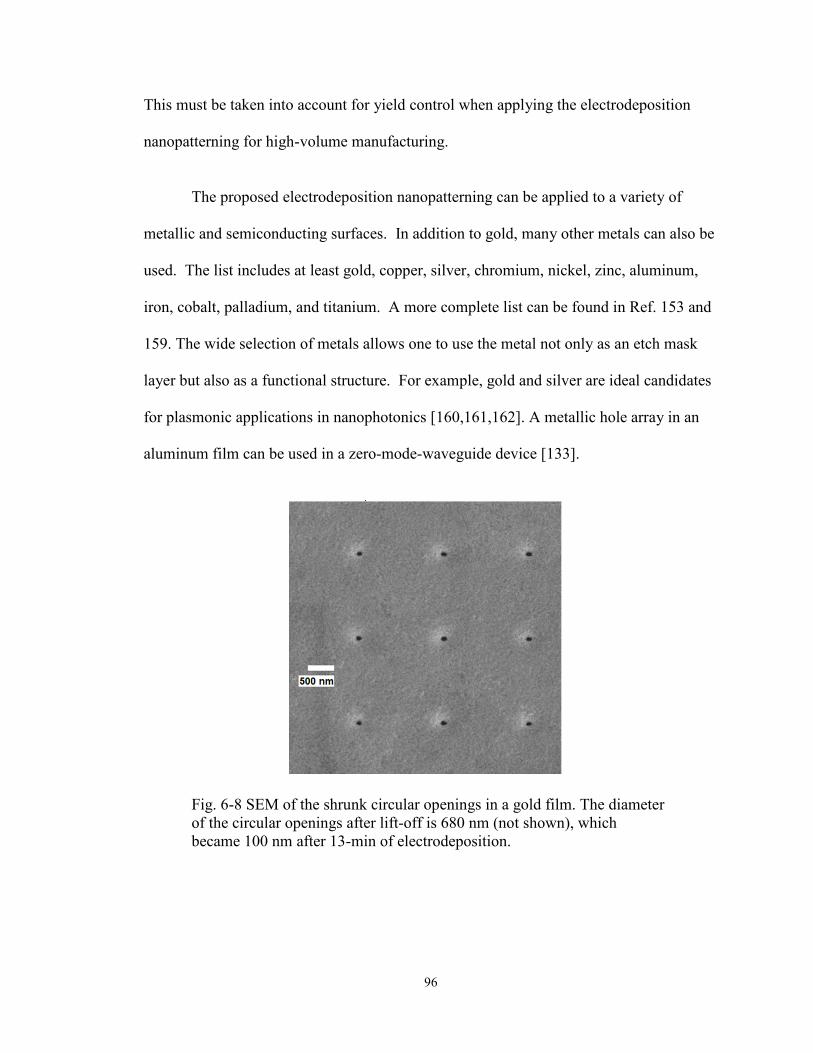
96
This must be taken into account for yield control when applying the electrodeposition
nanopatterning for high-volume manufacturing.
The proposed electrodeposition nanopatterning can be applied to a variety of
metallic and semiconducting surfaces. In addition to gold, many other metals can also be
used. The list includes at least gold, copper, silver, chromium, nickel, zinc, aluminum,
iron, cobalt, palladium, and titanium. A more complete list can be found in Ref. 153 and
159. The wide selection of metals allows one to use the metal not only as an etch mask
layer but also as a functional structure. For example, gold and silver are ideal candidates
for plasmonic applications in nanophotonics [160,161,162]. A metallic hole array in an
aluminum film can be used in a zero-mode-waveguide device [133].
Fig. 6-8 SEM of the shrunk circular openings in a gold film. The diameter of the circular openings after lift-off is 680 nm (not shown), which became 100 nm after 13-min of electrodeposition.

97
6.4 Challenges for the Electrodeposition Shrinkage Technique
In the middle of an attempt to shrink the hole diameter down to sub-20 nm, we
found that there were, on the electrodeposited surface, colloidal grains with grain size ~
20 nm even with just 2 minutes of deposition. This means that we will lose the control of
the aperture shrinkage when we approach the 20-nm diameter, when the grain size is
even larger than the aperture. We are investigating whether the ~ 20-nm grain size is just
an unfortunate accident of that particular set of experiment, or the sub-20-nm process
requires a tailored condition for electrodeposition.
6.5 Summary
We proposed and demonstrated an accurate and repeatable sub-10 nm patterning
technique that is fully compatible with other pattern-transfer processes as well as SAE.
Diameter of nanoscale apertures was reduced from 30 nm to 7 nm after performing an
atomic-layer deposition (ALD) on the apertures’ sidewall followed by an anisotropic
reactive-ion etching (RIE) to re-open the apertures. Subsequent pattern-transfer was
demonstrated as sub-10 nm gold nanodots after lift-off. The proposed technique only
requires commonly available nanofabrication facilities. This technique opens the
opportunities for SAE of nanometer-scale (7 nm) III-nitride QDs. On the other hand, this
technique is compatible with the top-down etching approach and can be used to fabricate
nano-etch-mask that may result in sub-10 nm InGaN quantum disks.
For high throughput nanofabrication, a novel wafer-scale nanopatterning
technique using electrodeposition is proposed and demonstrated. Using only the standard
98
i-line lithography and electrodeposition processes, the space features including both
trenches and holes have been shrunk from about 700 nm to less than 100 nm over a wafer
area > 1 cm by 1 cm. The wafer area was only limited by a single field size in our i-line
stepper. The sub-100 nm features were successfully transferred to the underlying
substrate, validating the electrodeposition process in nanopatterning. We discussed the
LER, registration error, and pattern-dependent shrinking rate, e.g. enhanced deposition at
the corners, which are specific to the electrodeposition process. One limitation of the
electrodeposition nanopatterning is the density of the nanoscale features which is limited
by optical diffraction in optical lithography. In i-line lithography, this corresponds to
around 200 nm. In practical processing conditions, this may be much larger. However,
the ability of using only standard micro-lithographic tools to define nanoscale features for
mass production in many nano devices is still very attractive.

99
Chapter 7
Conclusions and Future Work
7.1 Research Summary
In this research, the two most common lithography-based approaches that enforce
site and dimension control to the epitaxial structures, the selective area epitaxy and the
top-down etching, were used to fabricate site- and dimension-controlled InGaN QDs. In
SAE, source supply mechanism, growth dynamics, growth rate anisotropy and growth
time are all critical in determining the structure and the associated optical properties of
the epi-structure. Because of this, a simple point-tracking model was developed to better
outline the epi-structure’s growth profile. Nanoscale SAE of III-nitride semiconductors
was demonstrated using a dielectric mask of 25-nm-diameter openings. We studied the
growth profile evolution of a high-density, site-controlled III-nitride nanodots which
were allowed to overgrow until nano-pyramids with 50-nm base diameters were formed.
Using the phase-field model, we were able to simulate the growth profile evolution,
which agreed qualitatively with the experimental results. We found that the dot was not

100
compact at the initial stage of the nanoscale SAE when the deposition via the mask
surface locally dominated the direct deposition onto the dot, which led to localized
growth rate enhancement near the dot edge. Later in the process, an orientation-
dependent growth rate coalesces various crystal planes and transforms these
nanostructures into a more uniform array. The experimental results were compared to the
results of theoretical studies using the phase-field method, and good agreement was
obtained. We also established site-controlled InGaN/GaN quantum dot arrays using the
same method. The InGaN QDs have diameter of 25 nm set by the nano-hole SAE mask,
dot height of 3 nm, and dot density of 1010 cm-2.
In parallel, we applied top-down etching approach to fabricate site- and
dimension-controlled InGaN QDs. The QDs are disk-shaped, having disk diameters from
~ 15 – 30 nm and a thickness of ~ 3 nm. RIE was used to etch down an InGaN SQW
patterned with Cr nanodots as etch masks. After etching, nanopillars were formed in
which the InGaN quantum disks are embedded. The tapered nanopillar sidewall is
thought to come from the mask faceting effect under RIE of high sputter-etching
components.
Photoluminescence measurement was carried out on the site-controlled InGaN
QDs. A broad FWHM linewidth was observed for SAE InGaN QDs despite high
structural uniformity (only 5 nm variation in dot diameter). Using the InGaN layer profile
calculated from the phase-field model, we determined the origin of the inhomogeneously
broadened PL linewidth observed from the SAE InGaN QDs to be from the non-uniform,
volcano-shaped InGaN layer, as a result of the enhance growth rate at the edge of the QD
during the earlier stage of SAE, caused mainly by the surface diffusion. On the other

101
hand, room-temperature quantum-dot-like luminescence was observed from a site-
controlled InGaN quantum disk fabricated by the top-down etching approach. The single-
disk emission was strong enough to be captured in real-time by a CCD camera, which is
not common for group-III single QD at room-temperature. Using µ-PL, we studied the
optical properties of the single InGaN quantum disk and compared the results with
theoretical modeling. The single-disk PL fitted well with the calculated emission from a
single quantum dot. Wavelength tuning due to quantum confinement in the InGaN disk
plane was also observed and modeled, and is speculated to originate from the built-in
electric field at the semiconductor/insulator interface. The results showed the importance
of the band edge shape on the emission wavelength. Temperature-dependent PL
measurement showed a lessened effect from the piezoelectric effect as well as a high
radiative efficiency at room temperature, both being attributed to carrier confinement and
reduced piezoelectric field in the InGaN layer. The emission linewidth of the single disk
was found to be profoundly influenced by the internal electric field present in all
directions of the quantum disk, resulting in abnormally large linewidth at low
temperature and a saturated linewidth above 100 K. A sidewall charge center (SCC)
model was proposed to explain the linewidth’s behavior.
Site-controlled QDs have the unique advantages of patterning-related scalability
and efficient device integration. From these perspectives with the focus on sub-10 nm III-
nitride QDs, we proposed and demonstrated an accurate and repeatable sub-10 nm
patterning technique that is fully compatible with other pattern-transfer processes as well
as SAE. Diameter of nanoscale apertures was reduced from 30 nm to 7 nm after
performing an atomic-layer deposition (ALD) on the apertures’ sidewall followed by an

102
anisotropic reactive-ion etching (RIE) to re-open the apertures. Subsequent pattern-
transfer was demonstrated as sub-10 nm gold nanodots after lift-off. The proposed
technique only requires commonly available nanofabrication facilities. This technique
opens the opportunities for SAE of sub-10 nm III-nitride QDs. Moreover, this technique
is also compatible with the top-down etching approach and can be used to fabricate nano-
etch-mask that may result in sub-10 nm InGaN quantum disks. For high throughput
nanofabrication, a novel wafer-scale nanopatterning technique using electrodeposition is
proposed and demonstrated. Using only the standard i-line lithography and
electrodeposition processes, the space features including both trenches and holes have
been shrunk from about 700 nm to less than 100 nm over a wafer area > 1 cm by 1 cm.
The wafer area was only limited by a single field size in our i-line stepper. The sub-100
nm features were successfully transferred to the underlying substrate, validating the
electrodeposition process in nanopatterning. One limitation of the electrodeposition
nanopatterning is the density of the nanoscale features. However, in cases when dense
patterns (< 500 nm separation between features) are not required e.g. sparse nano-
aperture devices used in bio-sensing, the option of using only standard micro-lithographic
tools to define nanoscale features for mass production is still very attractive.
In most cases, the applications will require III-nitride QDs to be integrated into
optical cavities. Here we introduced and demonstrated bandgap-selective PEC etching as
a method for making suspended III-nitride optical cavity (especially the PhC slab).
InGaN SL was used as a sacrificial layer which absorbed the laser excitation at 390 nm.
For PEC etching time of 75 minutes, an undercut was formed and extended to
approximately 1 μm underneath the GaN membrane, corresponding to an approximate

103
etch rate of 13 nm / min. Nanoscale filamentary residues were observed and was related
to the dislocation density on the GaN templates on which InGaN SL was grown. It was
found that by using a thicker, 5-um thick GaN template, the whiskers were almost absent
after the PEC etching, leaving a clean bottom surface on the GaN membrane.
7.2 Future Work
Rigorous QD Characterization
Immediate future work of this research will focus on the characterization of single
site-controlled InGaN QDs. Optical measurement for time-resolved μ-PL (TR μ-PL) is
being set up to probe the emission dynamics of the single disk. Time-correlated
measurement, the Hanbury Brown-Twiss measurement is also being set up to check the
presence of single-photon streams from the single-disk emission. These experiments can
help verify if the emission from the single quantum disk shares some of the QD’s
emission characteristics such as the emission of single-photon stream.
Nanometer-Scale Site-Controlled QD
Having iterated many times in this thesis, III-nitride QDs should have diameter
less than 4 nm such that their dimension is comparable to the de Broglie wavelength of
nitride semiconductors which is ~ 3.86 nm at room temperature. Various nanopatterning
techniques, namely the ALD shrinkage technique and the over-etching (see Chapter 3.1)
will be applied to the fabrication of sub-5 nm site- and dimension-controlled III-nitride
QDs.

104
Integration with Optical Cavities
Advantage of site- and dimension-controlled QD should be demonstrated as its
precise integration into photonic cavities. As mentioned in Chapter 5, an immediate plan
for integration will be to demonstrate a high-throughput, single-dot-in-PhC process by
just following common lithographic alignment procedures i.e. no additional processing is
required to locate individual dots. During e-beam lithography, the center (anti-node) of
PhC-slab cavity will be precisely aligned to the each single dot. The PhC slabs can be
fabricated by the PEC etching process described in Chapter 5.
Another type of optical cavity, the metal-cladded cavity, can be easily integrated
to the site-controlled InGaN quantum disks by depositing a conformal layer of metal onto
the alumina-coated nanopillars. Such single-dot device may have a potential for high-
speed (THz) modulation of the QD emission through the dot-cavity weak-coupling
(Purcell effect).

105
Bibliography
1. Khitrova, H. M. Gibbs, M. Kira, S. W. Koch and A. Scherer, Vacuum Rabi splitting in semiconductors, Nature Physics 2, 81 (2006).
2. C. Santori, D. Fattal, J. Vučković, G. S. Solomon, Y. Yamamoto, Indistinguishable photons from a single-photon device, Nature 419, 594 (2002).
3. A. J. Shields, Semiconductor quantum light sources, Nature Photon. 1, 215 (2007).
4. A. Imamoğlu, D. D. Awschalom, G. Burkard, D. P. DiVincenzo, D. Loss, M. Sherwin, and A. Small, Quantum information processing using quantum dot spins and cavity QED, Phys. Rev. Lett. 83, 4204 (1999).
5. E. K. Lau, A. Lakhani, R. S. Tucker, and M. C. Wu, Opt. Express 17, 7790 (2009).
6. T. Tawara, H. Gotoh, T. Akasaka, N. Kobayashi, and T. Saitoh, Cavity polaritons in InGaN microcavities at room temperature. Phys. Rev. Lett. 92 (25), 256402 (2004).
7. Y.-R. Wu, Y.-Y. Lin and J. Singh, InGaN Light Emitters: A comparison of Quantum Dot and Quantum Well Based Devices in CLEO/QELS (San Jose, CA, 2008).
8. D. Bimberg, M. Grundmann, and N. N. Ledentsov, Quantum Dot Heterostructures (John Wiley and Sons, West Sussex, 1999).
9. W. Huang and F. Jain, Enhanced optical gain in InGaN-AlGaN quantum wire and quantum dot lasers due to excitonic transitions. J. Appl. Phys. 87 (10), 7354-7359 (2000).
106
10. Y. Narukawa, Y. Kawakami, S. Fujita, S. Fujita and S. Nakamura, Recombination dynamics of localized excitons in In0.20Ga0.80N / In0.05Ga0.95N multiple quantum wells. Phys. Rev. B 55 (4), R1938 (1997).
11. N. Malkova and C. Z. Ning, Surface states of wurtzite semiconductor nanowires with identical lateral facets: A transfer-matrix approach. Phys. Rev. B 74, 155308 (2006).
12. B. Beschoten et al., Spin coherence and dephasing in GaN. Phys. Rev. B 63 (12), 121202 (2001).
13. G. Christmann, R. Butte, E. Feltin, J. F. Carlin and N. Grandjean, Impact of inhomogeneous excitonic broadening on the strong exciton-photon coupling in quantum well nitride microcavities. Phys. Rev. B 73 (15), 153305-153304 (2006).
14. A. D. Andreev, E. P. O'Reilly, Theory of the electronic structure of GaN/AlN hexagonal quantum dots. Phys. Rev. B 62 (23), 15851 (2000).
15. Y. Arakawa, Progress in GaN-based quantum dots for optoelectronics applications, IEEE Journal of Selected Topics in Quantum Electronics 8 (4), 823-832 (2002).
16. H. Gotoh, H. Ando and H. Kanbe, Excitonic optical properties in semiconductor thin quantum boxes of intermediate regime between zero and two dimensions. Appl. Phys. Lett. 68 (15), 2132-2134 (1996).
17. J. G. Lozano et al., Misfit relaxation of InN quantum dots: Effect of the GaN capping layer. Appl. Phys. Lett. 88 (15), 151913-151913 (2006).
18. V. C. Elarde, R. Rangarajan, J. J. Borchardt and J.J. Coleman, Room-temperature operation of patterned quantum-dot lasers fabricated by electron beam lithography and selective area metalorganic chemical vapor deposition. IEEE Photon. Technol. Lett. 17, 935 (2005).
19. V. C. Elarde, A. C. Bryce and J. J. Coleman, High performance laser with nanopatterned active layer by selective area epitaxy. Electron. Lett 41 (20), 1122-1124 (2005).
20. S. D. Hersee, X. Y. Sun and X. Wang, The controlled growth of GaN nanowires. Nano Lett. 6 (8), 1808-1811 (2006).
21. P. Chen, A. Chen, S. J. Chua and J.N. Tan, Growth and optical properties of highly uniform and periodic InGaN nanostructures. Adv. Mater. 19 (13), 1707-+ (2007).
107
22. P. Chen, S. J. Chua, Y. D. Wang, M. D. Sander and C. G. Fonstad, InGaN nanorings and nanodots by selective area epitaxy. Appl. Phys. Lett. 87 (14), 143111 (2005).
23. H. Hirayama et al., Intense photoluminescence from self-assembling InGaN quantum dots artificially fabricated on AlGaN surfaces, Applied Physics Letters 72, 1736 (1998).
24. K. Tachibana et al., Nanometer-scale InGaN self-assembled quantum dots grown by metalorganic chemical vapor deposition, Applied Physics Letters 74, 383 (1999).
25. K. Tachibana et al., Room-temperature lasing oscillation in an InGaN self-assembled quantum dot laser, Applied Physics Letters 75, 2605 (1999).
26. O. Moriwaki et al., Narrow photoluminescence peaks from localized states in InGaN quantum dot structures, Applied Physics Letters 76, 2361 (2000).
27. R. Seguin et al., Multi-excitonic complexes in single InGaN quantum dots, Applied Physics Letters 84, 4023 (2004).
28. Y. G. Musikhin et al., Influence of metalorganic chemical vapor deposition growth conditions on In-rich nanoislands formation in InGaN/GaN structures, Applied Physics Letters 80, 2099 (2002).
29. K. T. Lam and L. W. Ji., Fractal analysis of InGaN self-assemble quantum dots grown by MOCVD, Microelectronics Journal 38, 905 (2007).
30. R.-C. Tu et al., Ultra-high-density InGaN quantum dots grown by metalorganic chemical vapor deposition, Japanese Journal of Applied Physics 43, L264 (2004).
31. J. Zhang et al., InGaN self-assembled quantum dots grown by metalorganic chemical-vapor deposition with indium as the antisurfactant, Applied Physics Letters 80, 485 (2002).
32. R. A. Oliver et al., InGaN quantum dots grown by metalorganic vapor phase epitaxy employing a post-growth nitrogen anneal, Applied Physics Letters 83, 755 (2003).
33. Q. Wang et al., The influence of a capping layer on optical properties of self-assembled InGaN quantum dots, Appl. Phys. Lett. 101, 113520 (2007).
34. C. Adelmann et al., Self-assembled InGaN quantum dots grown by molecular-beam epitaxy, Appl. Phys. Lett. 76, 1570 (2000).

108
35. B. Damilano et al., Room-temperature blue-green emission from InGaN/GaN quantum dots made by strain-induced islanding growth, Applied Physics Letters 75, 3751 (1999).
36. I. Park et al., Effect of InGaN quantum dot size on the recombination process in light-emitting diodes, Applied Physics Letters 92, 253105 (2008).
37. Q. Wang et al., Growth and optical investigation of self-assembled InGaN quantum dots on a GaN surface using a high temperature AlN buffer, Journal of Applied Physics 103, 123522 (2008).
38. M. Sénès et al., Strong carrier confinement and negligible piezoelectric effect in InGaN/GaN quantum dots, Physica E 40, 2066 (2008).
39. Y.-K. Ee et al., Self-assembled InGaN quantum dots on GaN emitting at 520nm grown by metalorganic vapor-phase epitaxy, Journal of Crystal Growth 310, 2320 (2008).
40. L.-W. Ji et al., InGaN/GaN multi-quantum dot light-emitting diodes, Journal of Crystal Growth 263, 114 (2004).
41. K. Hiramatsu, Epitaxial lateral overgrowth techniques used in group III nitride epitaxy, Journal of Physics: Condensed Matter 13, 6961 (2001).
42. Y. Kawaguchi et al., Selective area growth of GaN using tungsten mask by metalorganic vapor phase epitaxy, Japanese Journal of Applied Physics 37, L845 (1998).
43. O. Kayser, Selective growth of InP/GaInAs in LP-MOVPE and MOMBE/CBE, Journal of Crystal Growth 107, 989 (1991).
44. H. Heinecke et al., Selective growth of GaAs in MOMBE and MOCVD systems, Journal of Crystal Growth 77, 303 (1986)
45. T. Kuech et al., Selective epitaxy in the conventional metalorganic vapor phase epitaxy of GaAs, Applied Physics Letters 54, 910 (1989)
46. K. Yamaguchi et al., Analysis of deposition selectivity in selective epitaxy of GaAs by metalorganic chemical vapor deposition, Japanese Journal of Applied Physics 29, 2351 (1990)
47. J. Yamaguchi and K. Okamoto, Lateral supply mechanisms in selective metalorganic chemical vapor deposition, Japanese Journal of Applied Physics 32, 1523 (1993).

109
48. J. Yamaguchi, J. Ogasawara, and K. Okamoto, Surface-diffusion models in selective metalorganic chemical vapor deposition, Journal of Applied Physics 72, 5919 (1992).
49. T. Ujihara et al., Pattern size effect on source supply process for sub-micrometer scale selective area growth by organometallic vapor phase epitaxy, Journal of Crystal Growth 289, 89 (2006)
50. Y. Kato et al., Selective growth of wurtzite GaN and AlxGa1-xN on GaN/sapphire substrates by metalorganic vapor phase epitaxy, Journal of Crystal Growth 144, 133 (1994)
51. M. Khenner et al., A model for isotropic crystal growth from vapor on a patterned substrate, Journal of Crystal Growth 235, 425 (2002)
52. K. Hiramatsu, K. Nishiyama, A. Motogaito, H. Miyake, Y. Iyechika, and T. Maeda, Recent progress in selective area growth and epitaxial lateral overgrowth of III-nitrides: Effects of reactor pressure in MOVPE growth, Physica Status Solidi (a) 176, 535 (1999).
53. J. Park, P. A. Grudowski, C. J. Eiting, and R. D. Dupuis, Selective-area and lateral epitaxial overgrowth of III–N materials by metal organic chemical vapor deposition, Applied Physics Letters 73, 333 (1998).
54. D. Kapolneka, S. Keller, R. Vetury, R. D. Underwood, P. Kozodoy, S. P. Den Baars, and U. K. Mishra, Anisotropic epitaxial lateral growth in GaN selective area epitaxy, Applied Physics Letters 71, 1204 (1997).
55. S. Srinivasan, M. Stevens, F. A. Ponce, and T. Mukai, Polychromatic light emission from single InGaN quantum wells grown on pyramidal GaN facets, Applied Physics Letters 87, 131911 (2005).
56. H. Yu, L. K. Lee, T. Jung, and P.-C. Ku, Photoluminescence study of semipolar {10-11} InGaN/GaN multiple quantum wells grown by selective area epitaxy, Applied Physics Letters 90, 141906 (2007).
57. L. K. Lee, T. Jung, and P.-C. Ku, Fabrication of site-controlled, highly uniform, and dense InGaN quantum dots, IEEE CLEO/QELS CThS2 (San Jose, CA, 2008).
58. T. Jung, Nano-structured InGaN Light-Emitting Diodes for Solid-State Lighting, University of Michigan, Ann Arbor (2009).
59. V. Pérez-Solórzano, A. Gröning, H. Schweizer, and M. Jetter, Evidence of different confinement regimes in site-controlled pyramidal InGaN structures, Physica Status Solidi. (b) 242, R97 (2005).

110
60. S. Osher and J. A. Sethian, Fronts propagating with curvature-dependent speed: algorithms based on Hamilton-Jacobi formulations, Journal of Computatiojnal Physics 79, 12 (1988).
61. D. Adalsteinsson and J. A. Sethian, A fast level set method for propagating interfaces, Journal of Computational Physics 118, 269 (1995).
62. Z. Li and B. Soni, Fast and accurate numerical approaches for Stefan problems and crystal growth, Numerical Heat Transfer, Part B 35, 461 (1999).
63. G. Russo and P. Smereka, A level-set method for the evolution of faceted crystals, SIAM Journal on Scientific Computing 21, 2073 (2000).
64. A. E. Romanov, T. J. Baker, S. Nakamura and J. S. Speck, Strain-induced polarization in wurtzite III-nitride semipolar layers, Journal of Applied Physics 100, 023522 (2006).
65. P. Waltereit, O. Brandt, A. Trampert, H. T. Grahn, J. Menniger, M. Ramsteiner, M. Reiche and K. H. Ploog, Nitride semiconductors free of electrostatic fields for efficient white light-emitting diodes, Nature 406, 865 (2000).
66. N. Akopian, G. Bahir, D. Gershoni, M. D. Craven, J. S. Speck and S. P. DenBaars, Optical evidence for lack of polarization in (112¯ 0) oriented GaN/(AlGa)N quantum structures, Applied Physics Letters 86, 202104 (2005).
67. M. Ueda, K. Kojima, M. Funato, and Y. Kawakami, Y. Narukawa and T. Mukai, Epitaxial growth and optical properties of semipolar (112¯2) GaN and InGaN/GaN quantum wells on GaN bulk substrates, Applied Physics Letters 89, 211907 (2006).
68. S. Srinivasan, M. Stevens, F. A. Ponce, H. Omiya and T. Mukai, Carrier dynamics and electrostatic potential variation in InGaN quantum wells grown on {11-22} GaN pyramidal planes, Applied Physics Letters 89, 231908 (2006).
69. K. Sebald, H. Lohmeyer, J. Gutowski, T. Yamaguchi and D. Hommel, Micro-photoluminescence of InGaN/GaN quantum dots up to 150 K, Physica Status Solidi (b) 243, 1661 (2006).
70. S. Christopoulos et al., Room-temperature polariton lasing in semiconductor microcavitites, Physical Review Letters 98, 126405 (2007).
71. M. Eichfelder, W.-M. Schulz, M. Reischle, M. Wiesner, R. Roßbach, M. Jetter and P. Michler, Room-temperature lasing of electrically pumped red-emitting InP/(Al0.20Ga0.80)0.51In0.49P quantum dots embedded in a vertical microcavity, Appl. Phys. Lett. 95, 131107 (2009).

111
72. D. W. Xu, S. F. Yoon, C. Z. Tong, L. J. Zhao, Y. Ding and W. J. Fan, High-temperature continuous-wave single-mode operation of 1.3-µm p-doped InAs-GaAs quantum-dot VCSELs, IEEE Photonics Technology Letters 21, 1211 (2009).
73. C. Schneider, T. Heindel, A.Huggenberger, P. Weinmann, C. Kristner, M. Kamp, S. Reitzenstein, S. Höfling, and A. Forchel, Appl. Phys. Lett. 94, 111111 (2009).
74. S. Keller, C. Schaake, N. A. Fichtenbaum, C. J. Neufeld, Y. Wu, K. McGroddy, A. David, S. P. DenBaars, C. Weisbuch, J. S. Speck, and U. K. Mishra, J. Appl. Phys. 100, 054314 (2006).
75. Y. He, L. Chen, Y.-K. Song, A. V. Nurmikko, S.-R. Jeon, Z. Ren, M. Gherasimova, and J. Han, Phys. Status Solidi C 2, 2740 (2005).
76. H.-S. Chen, D.-M. Yeh, Y.-C. Lu, C.-Y. Chen, C.-F. Huang, T.-Y. Tang, C.-C. Yang, C.-S. Wu, and C.-D. Chen, Nanotechnology 17, 1454 (2006).
77. V. Ramesh, A. Kikuchi, K. Kishino, M. Funato, and Y. Kawakami, J. Appl. Phys. 107, 114303 (2010).
78. P. Yu, C. H. Chiu, Y.-R. Wu, H. H. Yen, J. R. Chen, C. C. Kao, H.-W. Yang, H. C. Kuo, T. C. Lu, W. Y. Yeh, and S. C. Wang, Appl. Phys. Lett. 93, 081110 (2008).
79. R. Steffen, Th. Koch, J. Oshinowo, F. Faller, and A. Forchel, Photoluminescence study of deep etched InGaAs/GaAs quantum wires and dots defined by low-voltage electron beam lithography, Applied Physics Letters 68, 223 (1996).
80. G. Mayer, B. E. Maile, R. Germann, A. Forchel, P. Grambow and H. P. Meier, Time-resolved investigations of sidewall recombination in dry-etched GaAs wires, Applied Physics Letters 56, 2016 (1990).
81. S. Keller, C. Schaake, N. A. Fichtenbaum, C. J. Neufeld, Y. Wu, K. McGroddy, A. David, S. P. DenBaars, C. Weisbuch, J. S. Speck and U. K. Mishra, Optical and structural properties of GaN nanopillar and nanostripe arrays with embedded InGaN/GaN multi-quan tum wells, Journal of Applied Physics 100, 054314 (2006).
82. D. A. Stocker, E. F. Schubert, and J. M. Redwing, Crystallographic wet chemical
etching of GaN, Appl. Phys. Lett. 73, 2654 (1998).
83. S. J Pearton, C R. Abernathy, and F. Ren, Gallium Nitride Processing for Electronics, Sensors and Spintronics (Springer, London, 2006).
84. S. J. Pearton, R. J. Shul, and F. Ren, A review of dry etching of GaN and related materials, MRS Internet J. Nitride Semicond. Res. 5, 11 (2000).

112
85. J. B. Schlager, K. A. Bertness, P. T. Blanchard, L. H. Robins, A. Roshko, and N. A. Sanford, J. Appl. Phys. 103, 124309 (2008).
86. E. V. Konenkova, Modification of GaAs(100) and GaN(0001) surfaces by treatment in alcoholic sulfide solutions, Vacuum 67, 43 (2002).
87. V. Pérez-Solórzano, A. Gröning, M. Jetter, T. Riemann, and J. Christen, Appl. Phys. Lett. 87, 163121 (2005).
88. A. F. Jarjour, R. A. Oliver, A. Tahraoui, M. J. Kappers, R. A. Taylor, and C. J. Humphreys, Superlattice. Microst. 43, 431 (2008).
89. A. F. Jarjour, R. A. Oliver, and R. A. Taylor, Philos. Mag. 87, 2077 (2007).
90. H.-C. Yu, H.-Y. Chen, and K. Thornton, http://arxiv.org/abs/0912.1288
91. S. Aland, J. Lowengrub, and A. Voigt, Computer Modeling in Engineering and Sciences (CMES) 57, 77 (2010).
92. H.-Y Chen, H.-C. Yu, and K. Thornton, J. Power Sources 196, 1333 (2011).
93. V. Jindal and F. Shahedipour-Sandvik, J. Appl. Phys. 106, 083115 (2009).
94. M. Khenner, R. J. Braun, M. G. Mauk, J. Cryst. Growth 241, 330 (2002).
95. J. Heinrich, A. Huggenberger, T. Heindel, S. Reitzenstein, S. Höfling, L. Worschech, and A. Forchel, Appl. Phys. Lett. 96, 211117 (2010).
96. M. J. Madou, Fundamentals of Microfabrication: The Science of Miniaturization, 2nd Ed. (CRC Press LLC, Boca Raton, 2002), chap. 2.
97. S. L. Chuang, Physics of Optoelectronic Devices (Wiley-Interscience, New York, 1995), pp. 157-160, 345-351.
98. I. Vurgaftman and J. R. Meyer, J. Appl. Phys. 94, 3675 (2003).
99. H. Zhao, G. Liu, and N. Tansu, Appl. Phys. Lett. 97, 131114 (2010).
100. P. Bogusławski, E.L. Briggs, and J. Bernholc, Phys. Rev. B 51, 17255 (1995).
101. Y.-H. Cho, G. H. Gainer, A. J. Fischer, J. J. Song, S. Keller, U. K. Mishra, and S. P. DenBaars, Appl. Phys. Lett. 73, 1370 (1998).
102. S. Kako, C. Santori, K. Hoshino, S. Götzinger, Y. Yamamoto, and Y. Arakawa, Nature Mater. 5, 887 (2006).
113
103. J.H. Rice, J.W. Robinson, J.D. Smith, A. Jarjour, R. A. Taylor, R. A. Oliver, G. Andrew, D. Briggs, M.J. Kappers, S. Yasin, and C.J. Humphreys, IEEE Trans. Nanotechnol. 3, 343 (2004).
104. H. Schӧmig, S. Halm, A. Forchel, G. Bacher, J. Off, and F. Scholz, Phys. Rev. Lett. 92, 106802 (2004).
105. S. A. Empedocles and M. G. Bawendi, Science 278, 2114 (1997).
106. S. Kako, K. Hoshino, S. Iwamoto, S. Ishida, and Y. Arakawa, Appl. Phys. Lett. 85, 64 (2004).
107. J. H. Rice, J. W. Robinson, A. Jarjour, R. A. Taylor, R. A. Oliver, G. Andrew, D. Briggs, M. J. Kappers, and C. J. Humphreys, Appl. Phys. Lett. 84, 4110 (2004).
108. Q. Song, H. Cao, S. T. Ho and G. S. Solomon, Near-IR subwavelength microdisk lasers, Applied Physics Letters 94, 061109 (2009).
109. M. Lipson, Guiding, modulating, and emitting light on silicon — challenges and opportunities, Journal of Lightwave Technology 23, 4222 (2005).
110. E. Yablonovitch, Phys. Rev. Lett. 58, 2059 (1987).
111. J.-F. Carlin, C. Zellweger, J. Dorsaz, S. Nicolay, G. Christmann, E. Feltin, R. Butté, and N. Grandjean, Progresses in III-nitride distributed Bragg reflectors and microcavities using AlInN/GaN materials, Physica Status Solidi (b) 242, 2326 (2005).
112. C. F. R. Mateus, M. C. Y. Huang,Y. Deng, A. R. Neureuther, and C. J. Chang-Hasnain, Ultrabroadband Mirror Using Low-Index Cladded Subwavelength Grating, IEEE Photonics Technology Letters 16, 518 (2004).
113. M. Arita, S. Ishida, S. Kako, S. Iwamoto, and Y. Arakawa, AlN air-bridge photonic crystal nanocavities demonstrating high quality factor, Appl. Phys. Lett. 91, 051106 (2007).
114. A. R. Stonas, N. C. MacDonald, K. L. Turner, S. P. DenBaars, and E. L. Hu, Photoelectrochemical undercut etching for fabrication of GaN microelectromechanical systems, J. Vac. Sci. Technol. B 19, 2828 (2001).
115. E. D. Haberer, R. Sharma, A. R. Stonas, S. Nakamura, S. P. DenBaars, and E. L.
Hu, Removal of thick (>100 nm) InGaN layers for optical devices using bandgap-selective photoelectrochemical etching, Appl. Phys. Lett. 85, 762 (2004).

114
116. C. Meier, K. Hennessy, E. D. Haberer, R. Sharma, Y.-S. Choi, K. McGroddy, S. Keller, S. P. DenBaars, S. Nakamura, and E. L. Hu, Visible resonant modes in GaN-based photonic crystal membrane cavities, Appl. Phys. Lett. 88, 031111 (2006).
117. M. J. Madou, Fundamentals of Microfabrication: The Science of Miniaturization, 2nd Ed. (CRC Press LLC, Boca Raton, 2002), chap. 4.
118. C.-T. Lee, H.-W. Chen, F.-T. Hwang, and H.-Y. Lee, Investigation of Ga oxide films directly grown on n-type GaN by photoelectrochemical oxidation using He-Cd laser, J. Electron. Mater. 34, 282 (2005).
119. Y. Youtsey, L. T. Romano, and I. Adesida, Gallium nitride whiskers formed by selective photoenhanced wet etching of dislocations, Appl. Phys. Lett. 73, 797 (1998).
120. S. Y. Chou, P. R. Krauss, W. Zhang, L. Guo and L. Zhuang, Sub-10 nm imprint lithography and applications, Journal of Vacuum Science and Technology B 15, 2897 (1997).
121. C. J. Lo, T. Aref and A. Bezryadin, Fabrication of symmetric sub-5 nm nanopores using focused ion and electron beams, Nanotechnoloy 17, 3264 (2006).
122. A. J. Storm, J. H. Chen, X. S. Ling, H.W. Zandbergen and C. Dekker, Fabrication of solid-state nanopores with single-nanometre precision, Nature Materials 2, 537 (2003).
123. P. Chen, M.-Y. Wu, H. W. M. Salemink and P. F. A. Alkemade, Fast single-step fabrication of nanopores, Nanotechnoloy 20, 015302 (2009).
124. J. Li, D. Stein, C. McMullan, D. Branton, M. J. Aziz and J. A. Golovchenko, Ion-beam sculpting at nanometer length scales, Nature 412, 166 (2001).
125. A. N. Broers, Resolution limits for electron-beam lithography, IBM Journal of Research Development 32, 502 (1988).
126. E. A. Dobisz, S. L. Brandow, R. Bass and J. Mitterender, Effects of molecular properties on nanolithography in polymethyl methacrylate, Journal of Vacuum Science and Technology B 18, 107 (2000).
127. A. Olzierski and I. Raptis, Development and molecular-weight issues on the lithographic performance of poly (methyl methacrylate), Microelectronic Engineering 73-74, 244 (2004).
115
128. A. Kokkinis, E.S. Valamontes, D. Goustouridis, Th. Ganetsos, K. Beltsios, I. Raptis, Molecular weight and processing effects on the dissolution properties of thin poly(methyl methacrylate) films, Microelectronic Engineering 85, 93 (2008).
129. S. Yasin, D. G. Hasko and H. Ahmed, Fabrication of <5 nm width lines in poly(methylmethacrylate) resist using a water:isopropyl alcohol developer and ultrasonically-assisted development, Applied Physics Letters 78, 2760 (2001).
130. J. M. Ryan, A. C. F. Hoole, and A. N. Broers, A study of the effect of ultrasonic agitation during development of poly(methylmethacrylate) for ultrahigh resolution electron-beam lithography, Journal of Vacuum Science and Technology B 13, 3035 (1995).
131. W. Hu, K. Sarveswaran, M. Lieberman and G. H. Bernstein, Sub-10 nm electron beam lithography using cold development of poly.methylmethacrylate, Journal of Vacuum Science and Technology B 22, 1711 (2004).
132. P. Chen et al., “Atomic layer deposition to fine-tune the surface properties and diameters of fabricated nanopores” Nano Letters 4, 1333 (2004).
133. M. J. Levene, J. Korlach, S. W. Turner, M. Foquet, H. G. Craighead, and W. W. Webb, Science 299, 682 (2003).
134. M. Foquet, K. T. Samiee, X. Kong, B. P. Chauduri, P. M. Lundquist, S. W. Turner, J. Freudenthal, and D. B. Roitman, J. Appl. Phys. 103, 034301 (2008).
135. Y. T. Yang, K. L. Ekinci, M. H. Huang, L. M. Schiavone, and M. L. Roukes, Appl. Phys. Lett. 78, 162 (2001).
136. M. Li, H. X. Tang, and M. L. Roukes, Nat. Nanotechnol. 2, 114 (2007).
137. S. Matsui, Proc. IEEE 85, 629 (1997).
138. S. Y. Chou, P. R. Krauss, W. Zhang, L. Guo, and L. Zhuang, J. Vac. Sci. Technol. B 15, 2897 (1997).
139. N. Li, W. Wu, and S. Y. Chou, Nano Lett. 6, 2626 (2006).
140. T. Balla, S. M. Spearing, and A. Monk, J. Phys. D: Appl. Phys. 41, 174001 (2008).
141. J. C. Hulteen and R. P. Van Duyne, J. Vac. Sci. Technol. A 13, 1553 (1995).
142. S. R. J. Brueck, Proc. IEEE 93, 1704 (2005).
143. X. Yang, H. Gentile, A. Eckert, and S. R. Brankovic, J. Vac. Sci. Technol. B 22, 3339 (2004).

116
144. F.-H. Ko, H.-C. You, T.-C. Chu, T.-F. Lei, C.-C. Hsu, and H.-L. Chen, Microelectron. Eng. 73, 323 (2004).
145. J.-Y. Yoon, M. Hata, J.-H. Hah, H.-W. Kim, S.-G. Woo, H.-K. Cho, and W.-S. Han, Proc. SPIE 5376, 196 (2004).
146. G. Lee, J. Park, W. Lee, C. Bok, C. Lim, and S. Moon, Proc. SPIE 5753, 181 (2005).
147. R. Peters, P. Montgomery, C. Garza, S. Filipiak, T. Stephens, and D. Babbitt, Proc. SPIE 5753, 195 (2005).
148. J.-W. Lee, Z. Feng, R. L. Engelstad, and E. G. Lovell, Proc. SPIE 5256, 1045 (2003).
149. A. F. Morpurgo, C. M. Marcus, and D. B. Robinson, Appl. Phys. Lett. 74, 2084 (1999).
150. A. Umeno and K. Hirakawa, Appl. Phys. Lett. 86, 143103 (2005).
151. E. J. Menke, M. A. Thomson, C. Xiang, L. C. Yang, and R. M. Penner, Nat. Mater. 5, 914 (2006).
152. T. P. Moffat, D. Wheeler, M. D. Edelstein, and D. Josell, IBM J. Res. Dev. 49, 19 (2005).
153. A. K. Graham, Electroplating Engineering Handbook, 3rd Ed., edited by A. K. Graham (Van Nostrand Reinhold Company, New York, 1971), Ch. 2, 4, 6.
154. J. Deconinck, J. Appl. Electrochem. 24, 212 (1994).
155. M. Hughes, N. Strussevitch, C. Bailey, K. McManus, J. Kaufmann, D. Flynn, and M. P. Y. Desmulliez, Int. J. Numer. Meth. Fluids DOI: 10.1002/fld.2140 (2009).
156. M. J. Madou, Fundamentals of Microfabrication: The Science of Miniaturization, 2nd Ed. (CRC Press LLC, Boca Raton, 2002), pp. 14-31.
157. K. P. Wong, K. C. Chan, and T. M. Yue, Surf. Coat. Technol. 135, 91 (2000).
158. K. Asano, Y. K. Choi, T. J. King, and C. M. Hu, IEEE Trans. Electron. Dev. 48, 1004 (2001).
159. M. Schlesinger and M. Paunovic, Modern Electroplating, 4th Ed., edited by M. Schlesinger and M. Paunovic (John Wiley & Sons, New York, 2000).

117
160. T. Rindzevicius, Y. Alaverdyan, A. Dahlin, F. Hӧӧk, D. S. Sutherland, and M. Käll, Nano Lett. 5, 2335 (2005).
161. C. Genet and T. W. Ebbesen, Nature 445, 39 (2007).
162. Z. Liu, J. M. Steele, W. Srituravanich, Y. Pikus, C. Sun, and X. Zhang, Nano Lett. 5, 1726 (2005).
163. D. D. Koleske, A. E. Wickenden, R. L. Henry, J. C. Culbertson and M.E. Twigg, GaN decomposition in H2 and N2 at MOVPE temperatures and pressures, Journal of Crystal Growth 223, 466 (2001).
164. K. Hennessy et al., Quantum nature of a strongly coupled single quantum dot-cavity system. Nature 445 (7130), 896-899 (2007).
165. P. Gallo et al., Integration of site-controlled pyramidal quantum dots and photonic crystal membrane cavities. Appl. Phys. Lett. 92 (26), 263101-263103 (2008).
166. A. Kaschner et al., Micro-Raman and cathodoluminescence studies of epitaxial laterally overgrown GaN with tungsten masks: A method to map the free-carrier concentration of thick GaN samples. Appl. Phys. Lett. 76 (23), 3418-3420 (2000).
167. Ning Li, M. A., S. Kako, M. Kitamura, S. Iwamoto, Y. Arakawa,, Fabrication and optical characterization of III-nitride air-bridge photonic crystal with GaN quantum dots. Phys. Status Solidi C 4 (1), 90-94 (2007).
168. Y. S. Choi et al., GaN blue photonic crystal membrane nanocavities. Appl. Phys. Lett. 87 (24), 243101-243103 (2005).