RADIO FREQUENCY IDENTIFICATION RADIO FREQUENCY IDENTIFICATION ...
Electrical and Electronics Engineering: An International Journal (ELELIJ) Vol 4, No 2, May 2015
DOI : 10.14810/elelij.2015.4205 53
DELAY TIME ANALYSIS OF COMBINED CMOS RING
OSCILLATOR
Sadegh Biabanifard1, S. Mehdi Hosseini Largani 1 and Shahrouz Asadi2
1Microelectronic Lab, Shahid Beheshti University, G. C, Tehran 2Department of Communication Engineering, Shahid Beheshti University, G.C, Tehran
ABSTRACT
CMOS ring voltage controlled oscillator with combined delay stages is presented. Initially the general
condition of oscillators is discussed then two common inverters are introduced and their delay times are
calculated parametrically. Our analysis and parametrically calculations states that delay time of basic type
inverter changes in opposite direction compared with current starved inverter versus supply voltage
changing, so a combined schematic can be used to obtain better frequency stability. The result of
simulation by TSMC 0.18µm CMOS technology and HSPICE approve the analysis results. The simulated
proposed CMOS VCO reduced the oscillation frequency dependence to supply voltage considerably and is
appropriate for On-Chip applications since no passive element is used.
KEYWORDS
CMOS Ring Oscillator, Frequency Stability, CMOS Inverter, Delay Time
1.INTRODUCTION
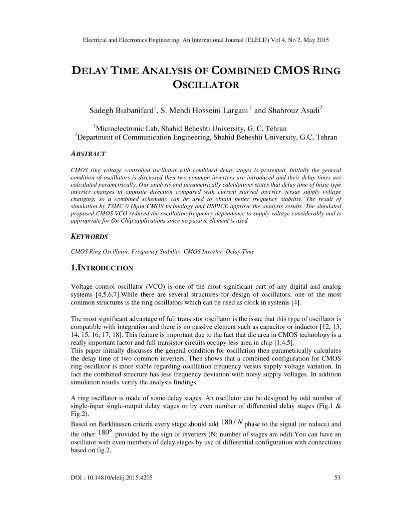
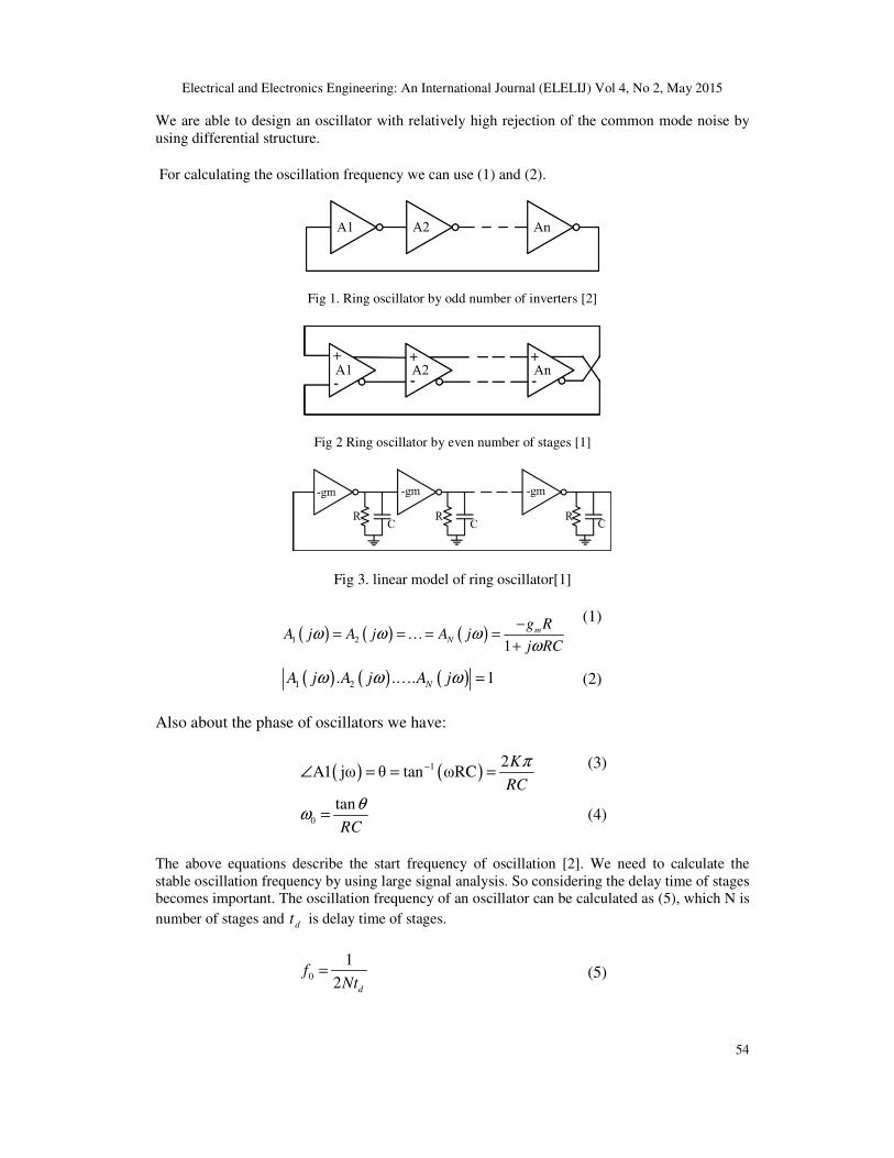
Voltage control oscillator (VCO) is one of the most significant part of any digital and analog systems [4,5,6,7].While there are several structures for design of oscillators, one of the most common structures is the ring oscillators which can be used as clock in systems [4]. The most significant advantage of full transistor oscillator is the issue that this type of oscillator is compatible with integration and there is no passive element such as capacitor or inductor [12, 13, 14, 15, 16, 17, 18]. This feature is important due to the fact that die area in CMOS technology is a really important factor and full transistor circuits occupy less area in chip [1,4,5]. This paper initially discusses the general condition for oscillation then parametrically calculates the delay time of two common inverters. Then shows that a combined configuration for CMOS ring oscillator is more stable regarding oscillation frequency versus supply voltage variation. In fact the combined structure has less frequency deviation with noisy supply voltages. In addition simulation results verify the analysis findings. A ring oscillator is made of some delay stages. An oscillator can be designed by odd number of single-input single-output delay stages or by even number of differential delay stages (Fig.1 & Fig.2).
Based on Barkhausen criteria every stage should add 180 / N phase to the signal (or reduce) and
the other 180° provided by the sign of inverters (N; number of stages are odd).You can have an oscillator with even numbers of delay stages by use of differential configuration with connections based on fig.2.
Electrical and Electronics Engineering: An International Journal (ELELIJ) Vol 4, No 2, May 2015
54
We are able to design an oscillator with relatively high rejection of the common mode noise by using differential structure. For calculating the oscillation frequency we can use (1) and (2).
Fig 1. Ring oscillator by odd number of inverters [2]
Fig 2 Ring oscillator by even number of stages [1]
Fig 3. linear model of ring oscillator[1]
( ) ( ) ( )1 21
mN
g RA j A j A j
j RCω ω ω
ω−
= = … = =+
(1)
( ) ( ) ( )1 2. . . 1N
A j A j A jω ω ω… =
(2)
Also about the phase of oscillators we have:
( ) ( )1 2A1 jω θ tan ωRC
K
RC
π−∠ = = =
(3)
0
tan
RC
θω =
(4)
The above equations describe the start frequency of oscillation [2]. We need to calculate the stable oscillation frequency by using large signal analysis. So considering the delay time of stages becomes important. The oscillation frequency of an oscillator can be calculated as (5), which N is
number of stages and dt is delay time of stages.
0
1
2 d
fNt
=
(5)

Electrical and Electronics Engineering: An International Journal (ELELIJ) Vol 4, No 2, May 2015
55
It is obvious from (5) that oscillation frequency depends only stages delay time since the number of stage in a fixed structure is constant. So delay time is the most important parameter for studying full transistor ring oscillator.
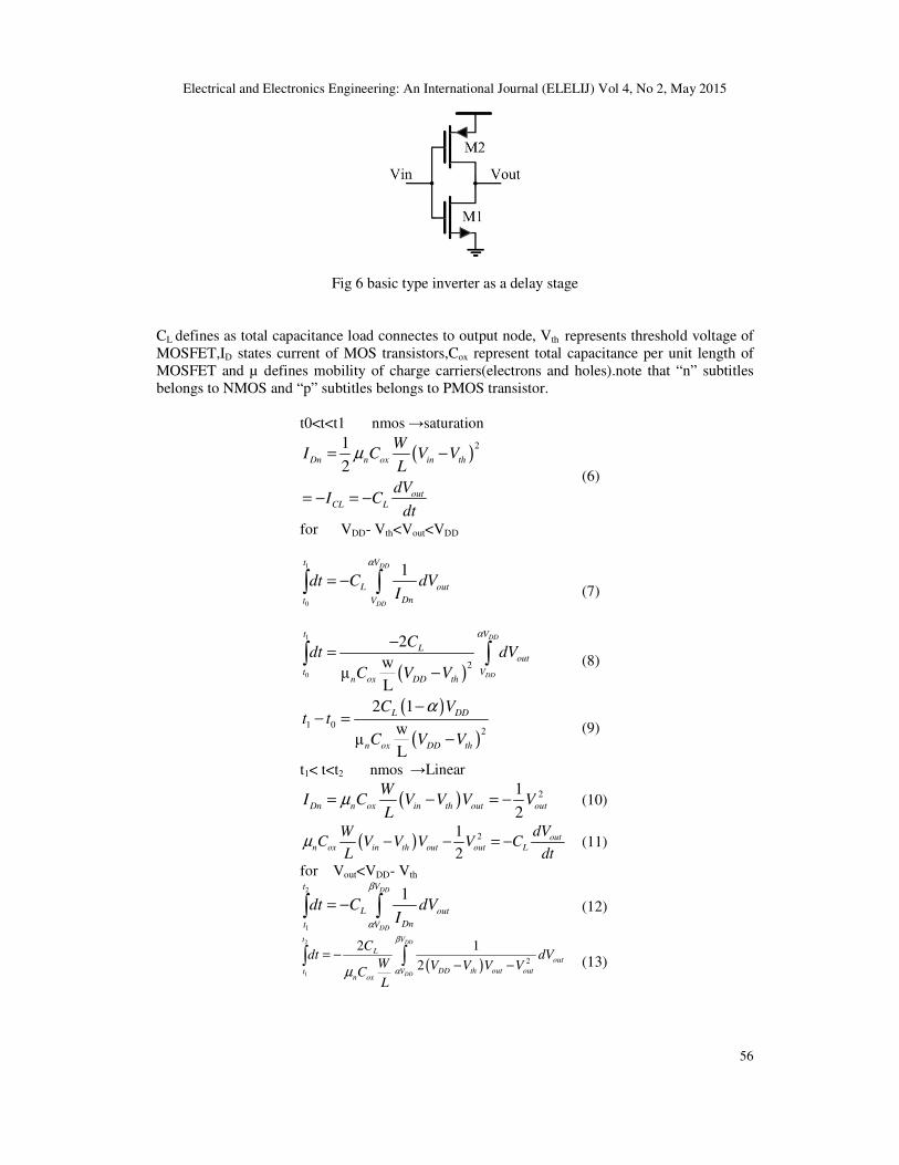
Fig 4. an inverter with delay time
2.DELAY TIMES General conditions of oscillations were discussed in previous part. In order to design a ring oscillator according to structure in previous section, we have to use inverters as delay stages. Regarding the delay time as the most important parameter in this kind of oscillator we should better calculate the delay time of stages. With the assumption of two inverters, basic type and current starved inverters (Fig.6 and Fig.7), we have calculated the delay times for these inverters with the aim of Fig.5. This figure shows the ideal input and typical out puts for inverters. Let’s
assume that delay time is proportional to 2 0t t− so it’s need to calculate 2 0t t−
as delay time. So we have for basic inverter:
Fig 5 input pulse and output of inverter
Electrical and Electronics Engineering: An International Journal (ELELIJ) Vol 4, No 2, May 2015
56
Fig 6 basic type inverter as a delay stage
CL defines as total capacitance load connectes to output node, Vth represents threshold voltage of MOSFET,ID states current of MOS transistors,Cox represent total capacitance per unit length of MOSFET and µ defines mobility of charge carriers(electrons and holes).note that “n” subtitles belongs to NMOS and “p” subtitles belongs to PMOS transistor.
t0<t<t1 nmos →saturation
( )21
2Dn n ox in th
outCL L
WI C V V
L
dVI C
dt
µ= −
= − = −
(6)
for VDD- Vth<Vout<VDD
1
0
1DD
DD
t V
L out
Dnt V
dt C dVI
α
= −∫ ∫
(7)
( )
1
0
2
2w
µL
DD
DD
t V
Lout
t Vn ox DD th
Cdt dV
C V V
α−
=−
∫ ∫
(8)
( )
( )1 0
2
2 1
wµ
L
L DD
n ox DD th
C Vt t
C V V
α−− =
−
(9)
t1< t<t2 nmos →Linear
( ) 21
2Dn n ox in th out out
WI C V V V V
Lµ= − = −
(10)
( ) 21
2out
n ox in th out out L
dVWC V V V V C
L dtµ − − = −
(11)
for Vout<VDD- Vth 2
1
1DD
DD
t V
L out
Dnt V
dt C dVI
β
α
= −∫ ∫
(12)
( )
2
1
2
2 1
2
DD
DD
t V
Lout
DD th out outt Vn ox
Cdt dV
W V V V VC
L
β
αµ= −
− −∫ ∫
(13)
Electrical and Electronics Engineering: An International Journal (ELELIJ) Vol 4, No 2, May 2015
57
( )2 1
2lnL
n ox DD th
Ct t
WC V V
L
α ββµ
−− =
−
α β>
(14)
( ) ( )9 14 delay time⇒+
( ) ( )2 0 2 1 1 0delayt t t t t t t∝ − = − + −
( )
( ) ( )2
2 1 2ln
delay
L L
n ox DD th
t
C VDD C
W Wn Cox VDD Vt C V V
L L
α α ββµ µ
∝
− −+
− −
(15)
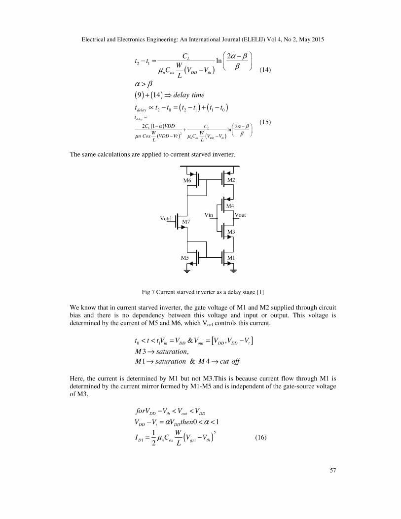
The same calculations are applied to current starved inverter.
Fig 7 Current starved inverter as a delay stage [1]
We know that in current starved inverter, the gate voltage of M1 and M2 supplied through circuit bias and there is no dependency between this voltage and input or output. This voltage is determined by the current of M5 and M6, which Vctrl controls this current.
[ ]0 1 & ,in DD out DD DD tt t t V V V V V V< < = = −
3 ,M saturation→ 1 & 4 M saturation M cut off→ →
Here, the current is determined by M1 but not M3.This is because current flow through M1 is determined by the current mirror formed by M1-M5 and is independent of the gate-source voltage of M3.
DD th out DDforV V V V− < <
0 1DD t DDV V V thenα α− = < <
( )2
1 1
1
2D n ox gs th
WI C V V
Lµ= −
(16)
Electrical and Electronics Engineering: An International Journal (ELELIJ) Vol 4, No 2, May 2015
58
( )2
1
1
2
Lout
n ox gs th
Cdt dV
wC V V
Lµ
= −−
(17)
1
0
1DD
DD
t V
L out
Dnt V
dt C dVI
α
= −∫ ∫
(18)
Know that ( )1gs thV V−
is a constant value.
( )
1
0
2
1
2 DD
DD
t V
Lout
t Vn ox gs th
Cdt dV
wC V V
L
α
µ
−=
−∫ ∫
(19)
( )
( )1 0 2
1
2 1L DD
n ox gs th
C Vt t
wC V V
L
α
µ
−− =
−
(20)
1 2
3 & 1
t t t
M linear M saturation
< <
→ →
( ) 23 3 3 3
1
2D n ox gs th ds ds
wI C V V V V
Lµ= − −
(21)
( )2
1 1
1
2D n ox gs th
wI C V V
Lµ= −
(22)
3L
outC D L
dVI I C
dt≅ − =
(23)
out DD thforV V V< −
2
1 3
1DD
DD
t V
L out
Dt V
dt C dVI
β
α
= −∫ ∫
(24)
( )
2
1
23 3 3
1
2
DD
DD
t
t
V
outL
Vn ox gs th ds ds
dt
dVC
wC V V V V
L
β
αµ
=
= −− −
∫
∫
(25)
3 1 3ds out ds out gs in DDV V V V andV V V= − ≅ ≅ =
( )
2
1
2
1DD
DD
t
t
V
Lout
DD th out outVn ox
dt
CdV
w V V V VC
L
β
αµ
=
= −− −
∫
∫
(26)
Electrical and Electronics Engineering: An International Journal (ELELIJ) Vol 4, No 2, May 2015
59
( )2 1
1lnL
DD thn ox
Ct t
w V VC
L
α ββµ
−− = −
(27)
( ) ( )20 27 delay time+ ⇒
( ) ( )
( )
( ) ( )
2 0 2 1 1 0
2
1
2 1ln
delay
delay
L DD L
n ox gs th n ox DD th
t t t t t t t
t
C V C
w wC V V C V V
L L
α α ββµ µ
∝ − = − + −
=
− −+
− −
(28)
By assuming supply voltage deviation we can write:
DD DD
A Bt of Basic Inverter
V V∆ ≅ +
∆ ∆ (29)
( )2 1
&
ln
L
n ox
L
n ox
CA
wC
L
CB
wC
L
α
µ
α ββµ
−≅
−≅
(30)
DD
DD
t of Current Starved Inverter
BD V
V
∆ ≅
× ∆ +∆
(31)
( )
( )2
1
2 1L
n ox gs th
CD
wC V V
L
α
µ
−≅
−
(32)
( ) ( )2
1 10 1 1gs th gs th
V V V V< − < → − �
( )
( )( )
2
1
2 1 2 1L L
n ox gs th n ox
C C
w wC V V C
L L
α α
µ µ
− −>
−
(33)
( )
( )2 1
ln2
1
C CL L
ww CC V V n oxn ox gs th LL
α α ββµµ
− −>
−
(34)
ln 1 & then D A D Bα β
β −
< > >
(35)
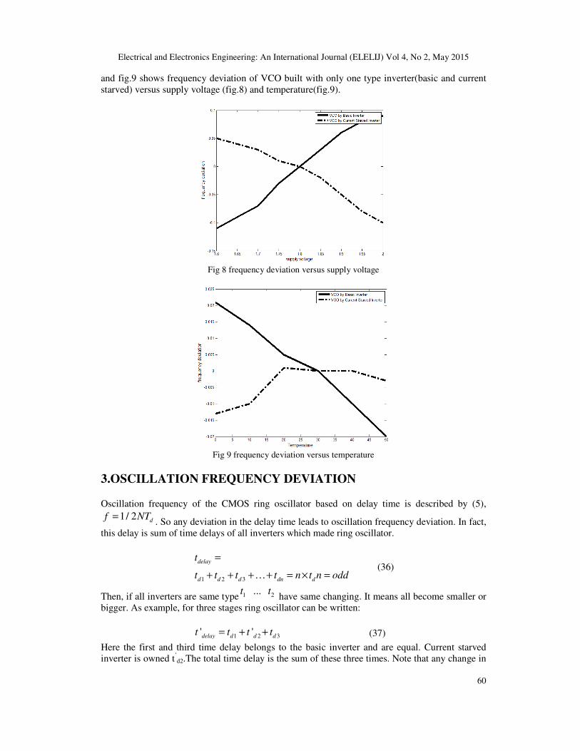
As a final result,∆t of basic inverter is proportional with 1 / ∆VDD, and ∆t of current starved inverter is proportional with ∆VDD. Regarding the delay times opposite variation for two mentioned inverters we can conclude that combined structure for ring oscillator is an appropriate technique to design a CMOS ring oscillator with decreasing the frequency deviation versus supply changing. As the fig.8 and fig.9 shows, the results are approved by the simulations. Fig.8
Electrical and Electronics Engineering: An International Journal (ELELIJ) Vol 4, No 2, May 2015
60
and fig.9 shows frequency deviation of VCO built with only one type inverter(basic and current starved) versus supply voltage (fig.8) and temperature(fig.9).
Fig 8 frequency deviation versus supply voltage
Fig 9 frequency deviation versus temperature
3.OSCILLATION FREQUENCY DEVIATION Oscillation frequency of the CMOS ring oscillator based on delay time is described by (5),
1/ 2 df NT=. So any deviation in the delay time leads to oscillation frequency deviation. In fact,
this delay is sum of time delays of all inverters which made ring oscillator.
1 2 3
delay
d d d dn d
t
t t t t n t n odd
=
+ + +…+ = × =
(36)
Then, if all inverters are same type 1 2...t t have same changing. It means all become smaller or
bigger. As example, for three stages ring oscillator can be written:
1 2 3' 'delay d d dt t t t= + + (37)
Here the first and third time delay belongs to the basic inverter and are equal. Current starved inverter is owned t’
d2.The total time delay is the sum of these three times. Note that any change in

Electrical and Electronics Engineering: An International Journal (ELELIJ) Vol 4, No 2, May 2015
61
the supply voltage changes delay times but as these changes are added together, they can reduce the effects of one another. Namely for three stages we have:
Fig 10.CMOS ring oscillator by three basic inverter(3delayt t∆ = ∆
) [11]
Fig 11 CMOS ring oscillator by two basic inverter and one current starved inverter
(' 2 'delayt t t∆ = ∆ + ∆
) [11] Considering the (38), by using combined configuration we can reduce the frequency deviation versus supply voltage changing. In fact the combined structure has more accurate oscillation frequency.
&
1' '
6 '
delay
osc osc
delay
t t
t t T cte
f f ctet
∆ ↑↔ ∆ ↓
∆ ↓↔ ∆ ↑→
′
′ ∆
= → ≅
′ ≅ (38)
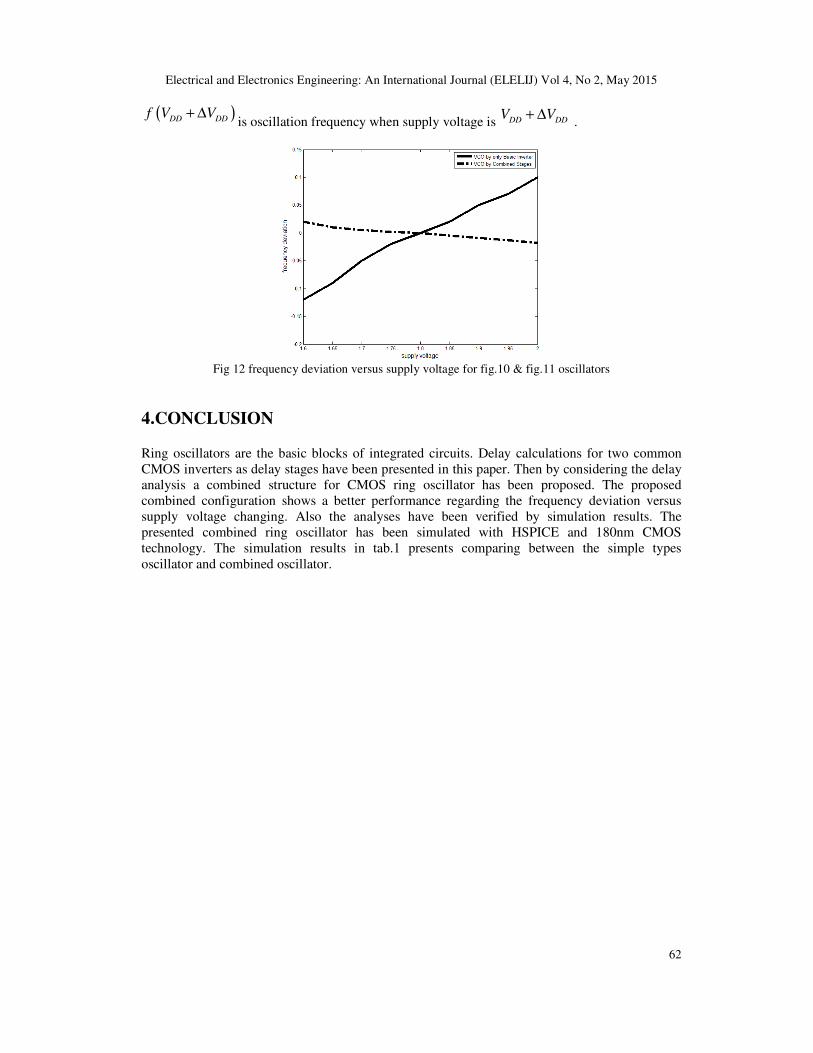
Frequency variations versus supply voltage for combined and basic ring oscillator have been shown in Fig.12. According to this figure combined configuration obtained better performance considering less frequency deviation. This can be verify by defining a factor as frequency deviation factor. Smaller value for this factor means better performance. It is obvious that combined ring oscillator has smaller value for this factor.
( ) ( )( )
DD DD DD
DD
f V V f Vf
f f V
+ ∆ −∆=
(39)
Electrical and Electronics Engineering: An International Journal (ELELIJ) Vol 4, No 2, May 2015
62
( )DD DDf V V+ ∆is oscillation frequency when supply voltage is DD DDV V+ ∆
.
Fig 12 frequency deviation versus supply voltage for fig.10 & fig.11 oscillators
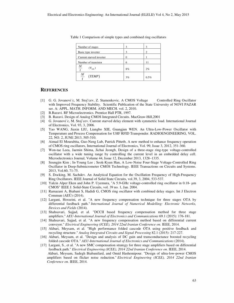
4.CONCLUSION Ring oscillators are the basic blocks of integrated circuits. Delay calculations for two common CMOS inverters as delay stages have been presented in this paper. Then by considering the delay analysis a combined structure for CMOS ring oscillator has been proposed. The proposed combined configuration shows a better performance regarding the frequency deviation versus supply voltage changing. Also the analyses have been verified by simulation results. The presented combined ring oscillator has been simulated with HSPICE and 180nm CMOS technology. The simulation results in tab.1 presents comparing between the simple types oscillator and combined oscillator.
Electrical and Electronics Engineering: An International Journal (ELELIJ) Vol 4, No 2, May 2015
63
Table 1 Comparison of simple types and combined ring oscillators
Number of stages 3 3
Basic type inverter 3 2
Current starved inverter 0 1
Number of transistor 6 11
)f
f(V
DD
∆
8% 2%
( )f
fTEMP
∆
3% 0.5%
REFERENCES
[1] G. G. Jovanovi´c, M. Stojˇcev, Z. Stamenkovic. A CMOS Voltage Controlled Ring Oscillator
with Improved Frequency Stability. Scientific Publication of the State University of NOVI PAZAR ser. A: APPL. MATH. INFORM. AND MECH. vol. 2, 2010.
[2] B.Razavi. RF Microelectronics. Prentice Hall PTR, 1997. [3] B. Razavi. Design of Analog CMOS Integrated Circuits. MacGraw-Hill,2001 [4] G. Jovanovi´c, M. Stojˇcev. Current starved delay element with symmetric load. International Journal
of Electronics, Vol. 93, 3, 2006. [5] Yao WANG, Jiaxin LIU, Liangbo XIE, Guangjun WEN. An Ultra-Low-Power Oscillator with
Temperature and Process Compensation for UHF RFID Transponder. RADIOENGINEERING, VOL. 22, NO. 2, JUNE 2013, 505-510.
[6] Aimad El Mourabita, Guo-Neng Lub, Patrick Pittetb, A new method to enhance frequency operation of CMOS ring oscillators, International Journal of Electronics, Vol. 99, Issue 3, 2012, 351-360.
[7] Won-tae Leea, Jaemin Shima, Jichai Jeongb, Design of a three-stage ring-type voltage-controlled oscillator with a wide tuning range by controlling the current level in an embedded delay cell. Microelectronics Journal, Volume 44, Issue 12, December 2013, 1328–1335.
[8] Seungjin Kim ; In-Young Lee ; Seok-Kyun Han, A Low-Noise Four-Stage Voltage-Controlled Ring Oscillator in Deep-Submicrometer CMOS Technology. IEEE Transactions on Circuits and Systems. 2013, Vol.60, 71-75.
[9] S. Docking, M. Sachdev. An Analytical Equation for the Oscillation Frequency of High-Frequency Ring Oscillators. IEEE Journal of Solid State Circuits, vol.39, 3, 2004, 533-537.
[10] Yalcin Alper Eken and John P. Uyemura, "A 5.9-GHz voltage-controlled ring oscillator in 0.18- µm CMOS" IEEE J. Solid-State Circuits, vol. 39 no. 1, Jan. 2004.
[11] Ramazani A, Biabani S, Hadidi G, CMOS ring oscillator with combined delay stages. Int J Electron Commun (AEÜ) (2014).
[12] Largani, Hosseini, et al. "A new frequency compensation technique for three stages OTA by differential feedback path." International Journal of Numerical Modelling: Electronic Networks,
Devices and Fields (2014). [13] Shahsavari, Sajjad, et al. "DCCII based frequency compensation method for three stage
amplifiers." AEU-International Journal of Electronics and Communications 69.1 (2015): 176-181. [14] Shahsavari, Sajjad, et al. "A new frequency compensation method based on differential current
conveyor." Electrical Engineering (ICEE), 2014 22nd Iranian Conference on. IEEE, 2014. [15] Akbari, Meysam, et al. "High performance folded cascode OTA using positive feedback and
recycling structure." Analog Integrated Circuits and Signal Processing 82.1 (2015): 217-227. [16] Akbari, Meysam, et al. "Design and analysis of DC gain and transconductance boosted recycling
folded cascode OTA." AEU-International Journal of Electronics and Communications (2014). [17] Largani, S., et al. "A new SMC compensation strategy for three stage amplifiers based on differential
feedback path." Electrical Engineering (ICEE), 2014 22nd Iranian Conference on. IEEE, 2014. Akbari, Meysam, Sadegh Biabanifard, and Omid Hashemipour. "Design of ultra-low-power CMOS
amplifiers based on flicker noise reduction." Electrical Engineering (ICEE), 2014 22nd Iranian
Conference on. IEEE, 2014.
Electrical and Electronics Engineering: An International Journal (ELELIJ) Vol 4, No 2, May 2015
64
Authors
Sadegh Biabanifard was born in Tehran, Iran in 1989. He received the B.S. degree in Electronic Engineering from Imam Reza International University, Mashhad, Iran in 2011 and M.S. degree in Analog Electronic from Shahid Beheshti University, G.C., Tehran, Iran, in 2014. His research interests are RFIC design, analog and mixed mode integrated circuit design for Ultra-Low-Power Ultra-Low-Voltage applications, OTA, current conveyer and data converter.
S. Mehdi Hosseini Largani, was born in Tonekabon, Iran in 1989. He received the B.S. degree in Control Engineering from K.N.Toosi University of Technology, Tehran, Iran in 2011 and M.S. degree in Analog Electronic from Shahid Beheshti University (National University of Iran) G.C., Tehran, Iran, in 2014. His research interests are analog and mixed mode circuit theory, integrated circuit design for Ultra-Low-Power Ultra-Low-Voltage applications. His is currently with Electrical Engineering Department and Microelectronic Research Laboratory in Shahid Beheshti University, G.C, Tehran, Iran.
Shahrooz Asadi received the B.Sc. degree in Electrical Engineering and the M.Sc. degree in Electronics both from Amirkabir University, Tehran, Iran, in 2003 and 2007, respectively and the Ph.D. degree in Electronics in the School of Information Technology and Engineering (SITE), University of Ottawa, Ottawa, ON, Canada. He joined shahidBeheshti University in 2011 where he is an assistant professor. His research interests include linear and nonlinear time-domain modeling of millimeter-wave transistors, RF design of active and passive devices, design and optimization of solid state devices and multiconductor transmission lines and printed circuit board