ABSTRACT Document: SINGLE-EVENT GATE RUPTURE IN POWER ...
171
ABSTRACT Title of Document: SINGLE-EVENT GATE RUPTURE IN POWER MOSFETS: A NEW RADIATION HARDNESS ASSURANCE APPROACH Jean-Marie Lauenstein, Ph.D. Candidate, 2011 Directed By: Professor Neil Goldsman, Department of Electrical and Computer Engineering Almost every space mission uses vertical power metal-semiconductor-oxide field-effect transistors (MOSFETs) in its power-supply circuitry. These devices can fail catastrophically due to single-event gate rupture (SEGR) when exposed to energetic heavy ions. To reduce SEGR failure risk, the off-state operating voltages of the devices are derated based upon radiation tests at heavy-ion accelerator facilities. Testing is very expensive. Even so, data from these tests provide only a limited guide to on-orbit performance. In this work, a device simulation-based method is developed to measure the response to strikes from heavy ions unavailable at accelerator facilities but posing potential risk on orbit. This work is the first to show that the present derating factor, which was established from non-radiation reliability concerns, is appropriate to reduce on-orbit SEGR failure risk when applied to data acquired from ions with appropriate penetration range. A second important outcome of this study is the
Transcript of ABSTRACT Document: SINGLE-EVENT GATE RUPTURE IN POWER ...

ABSTRACT
Title of Document: SINGLE-EVENT GATE RUPTURE IN POWER MOSFETS: A NEW RADIATION HARDNESS ASSURANCE APPROACH
Jean-Marie Lauenstein, Ph.D. Candidate, 2011
Directed By: Professor Neil Goldsman, Department of Electrical and Computer Engineering
Almost every space mission uses vertical power metal-semiconductor-oxide
field-effect transistors (MOSFETs) in its power-supply circuitry. These devices can
fail catastrophically due to single-event gate rupture (SEGR) when exposed to
energetic heavy ions. To reduce SEGR failure risk, the off-state operating voltages of
the devices are derated based upon radiation tests at heavy-ion accelerator facilities.
Testing is very expensive. Even so, data from these tests provide only a limited guide
to on-orbit performance.
In this work, a device simulation-based method is developed to measure the
response to strikes from heavy ions unavailable at accelerator facilities but posing
potential risk on orbit. This work is the first to show that the present derating factor,
which was established from non-radiation reliability concerns, is appropriate to
reduce on-orbit SEGR failure risk when applied to data acquired from ions with
appropriate penetration range. A second important outcome of this study is the
demonstration of the capability and usefulness of this simulation technique for
augmenting SEGR data from accelerator beam facilities.
The mechanisms of SEGR are two-fold: the gate oxide is weakened by the
passage of the ion through it, and the charge ionized along the ion track in the silicon
transiently increases the oxide electric field. Most hardness assurance methodologies
consider the latter mechanism only. This work demonstrates through experiment and
simulation that the gate oxide response should not be neglected. In addition, the
premise that the temporary weakening of the oxide due to the ion interaction with it,
as opposed to due to the transient oxide field generated from within the silicon, is
validated. Based upon these findings, a new approach to radiation hardness assurance
for SEGR in power MOSFETs is defined to reduce SEGR risk in space flight
projects.
Finally, the potential impact of accumulated dose over the course of a space
mission on SEGR susceptibility is explored. SEGR evaluation of gamma-irradiated
power MOSFETs suggests a non-significant SEGR susceptibility enhancement due to
accumulated dose from gamma rays. During SEGR testing, an unexpected enhanced
dose effect from heavy-ion irradiation was detected. We demonstrate that this effect
could be due to direct ionization by two or more ions at the same channel location.
The probability on-orbit for such an occurrence is near-zero given the low heavy-ion
fluence over a typical mission lifetime, and did not affect SEGR susceptibility.
The results of this work can be used to bound the risk of SEGR in power
MOSFETs considered for insertion into spacecraft and instruments.

SINGLE-EVENT GATE RUPTURE IN POWER MOSFETS: A NEW RADIATION HARDNESS ASSURANCE APPROACH
By
Jean-Marie Lauenstein
Dissertation submitted to the Faculty of the Graduate School of the University of Maryland, College Park, in partial fulfillment
of the requirements for the degree of Doctor of Philosophy
2011
Advisory Committee: Professor Neil Goldsman, Chair Professor Martin Peckerar Associate Professor Pamela Abshire Professor John Melngailis Professor Aris Christou

© Copyright by Jean-Marie Lauenstein
2011
ii
Dedication
To Karen Elaine Sanders
and
Julia Marie Dunn

iii
Acknowledgments
First and foremost, I extend my utmost appreciation and thanks to my advisor,
Professor Neil Goldsman, for his support, guidance, instruction, friendship, and
device-physics intuition. He led me into the deep, carrying the lantern to show me
the way.
I am thankful to my dissertation committee members, Professors Pamela
Abshire, Martin Peckerar, John Melngailis, and Aris Christou, for their time and
service.
This work was supported in part by the National Aeronautics and Space
Administration’s (NASA) Electronic Parts and Packaging Program, NASA Flight
Projects, the Defense Threat Reduction Agency under IACRO10-4977I, and the
NASA Goddard Space Flight Center Internal Research and Development Program.
This work was conducted in part using the resources of the Department of Electrical
and Computer Engineering at the University of Maryland, College Park, MD,
CoolCAD Electronics, College Park, MD, the Advanced Computing Center for
Research and Education at Vanderbilt University, Nashville, TN, and International
Rectifier Corporation, El Segundo, CA.
Special thanks for helpful technical discussions with and encouragement from
Raymond L. Ladbury, Sandra Liu, Max Zafrani, Jeffrey L. Titus, Kenneth A. LaBel,
Akin Akturk, Siddarth Potbhare, Jack Shue, Leif Z. Scheick, Timothy Oldham,
Michael Xapsos, Christian Poivey, Fredrik Sturesson, Véronique Ferlet-Cavrois,

iv
Robert A. Reed, Robert A. Weller, Ron Schrimpf, Kenneth F. Galloway, and Art F.
Witulski.
Assistance with experimental testing from Hak S. Kim and Anthony M. Phan is
gratefully acknowledged. Thank you to Ken LaBel for providing the latitude and
support to conduct these experiments. Technical assistance from Stephen Cox,
Timothy Irwin, Donald Hawkins, Martha O’Bryan, Donna Cochran, Stephen Brown,
Tom Ward, and Yevgeniy Gerashchenko is also acknowledged and appreciated.
Sometimes in our life, we are fortunate to find ourselves surrounded by
individuals who take on an unspoken role of mentor to us. I am blessed to have been
shepherded first into the radiation environment community by Janet Barth, then the
radiation effects community by Ray Ladbury and the power MOSFET world by Jack
Shue. I am particularly thankful for Ray’s open door, through which he never tired of
me entering at times seemingly daily.
Finally, my friends and family formed a tremendous support system through
this process. I am particularly grateful to Sue Kovalsky, Roxanne Corrado, Dee
Thorne, and Heather Podesek, who together rose to become extended family in their
unwavering care week in and week out.

v
Table of Contents
Dedication ii Acknowledgments....................................................................................................... iii Table of Contents ......................................................................................................... v
List of Tables ............................................................................................................ viii List of Figures ............................................................................................................. ix
Chapter 1: Introduction ............................................................................................... 1
1.1 Importance of Power MOSFETs in Space Missions ........................................ 1
1.2 Overview of the Space Radiation Environment ................................................ 3
1.3 Summary of Radiation Effects on Microelectronics ......................................... 8
1.3.1 Total Dose ................................................................................................... 8
1.3.2 Single-Event Effects ................................................................................. 12
1.4 Description of the Single-Event Gate Rupture Failure Mechanisms .............. 14
1.4.1 Initial Discovery and Understanding ........................................................ 14
1.4.2 Description of the Single-Event Gate Rupture Failure Mechanisms ........ 15
1.4.3 Use of MOS Capacitors to Study SEGR................................................... 18
1.5 Past Methods for Evaluating and Mitigating SEGR Likelihood .................... 19
1.5.1 Mission Requirement Specifications: Use of the LET Metric ................. 20
1.5.2 Evaluation of SEGR Likelihood ............................................................... 21
1.5.3 SEGR Mitigation Methods ....................................................................... 22
1.6 Deficiencies in Methodologies for Evaluating and Mitigating SEGR Susceptibility in Power MOSFETs ................................................................. 23
1.6.1 Limitations of Heavy-Ion Testing ............................................................. 23
1.6.2 Deficiencies of the LET Metric ................................................................ 26
1.6.3 SEGR Rate Considerations ....................................................................... 27
1.6.4 Limitations of Derating Practices ............................................................. 29
1.7 Overview of This Work .................................................................................. 31
Chapter 2: Evaluation of SEGR Mitigation Procedures in Power MOSFETs ......... 33
2.1 Motivation ....................................................................................................... 33
2.2 Experimental Methods .................................................................................... 35
2.3 Experimental Results ...................................................................................... 39
2.4 Simulation Methods ........................................................................................ 41
2.5 Simulation Results .......................................................................................... 44
2.5.1 200V Radiation-Hardened nVDMOS ....................................................... 44
2.5.2 500V Commercial pVDMOS ................................................................... 47
2.6 Discussion ....................................................................................................... 49
2.7 Conclusion ...................................................................................................... 51
Chapter 3: Studies of Ion Species Effects in SEGR Susceptibility of Power MOSFETs ................................................................................................ 54
3.1 Motivation ....................................................................................................... 54
3.2 Verification of the Titus-Wheatley Formula of the Critical Oxide Electric Field for SEGR ............................................................................................... 55

vi
3.2.1 Experimental Methods .............................................................................. 56
3.2.2 Results ....................................................................................................... 59
3.2.3 Implication for Simulation Methods of SEGR Prediction ........................ 61
3.3 Validation of the Experimental Method to Isolate the Critical Oxide Field for Gate Rupture ................................................................................................... 62
3.3.1 Simulation Methods .................................................................................. 63
3.3.2 Results ....................................................................................................... 63
3.3.3 Discussion ................................................................................................. 70
3.4 Two-Photon Absorption Laser Tests to Reveal the Criticality of Gate-Oxide Damage for SEGR .......................................................................................... 71
3.4.1 Purpose ...................................................................................................... 71
3.4.2 Sample Preparation and Experimental Methods ....................................... 72
3.4.3 Results ....................................................................................................... 75
3.4.4 Conclusions ............................................................................................... 76
3.4.5 Next Steps ................................................................................................. 77
3.5 Relative Roles of Heavy-Ion Interactions with the Oxide, Epilayer, and Substrate .......................................................................................................... 77
3.5.1 Experimental Methods .............................................................................. 78
3.5.2 Results ....................................................................................................... 80
3.5.3 Discussion and Implication for SEGR Hardness Assurance in Power MOSFETs ................................................................................................. 85
3.6 Summary ......................................................................................................... 88
Chapter 4: A New Hardness Assurance Approach for Bounding the On-Orbit Risk of SEGR .................................................................................................. 90
4.1 Applying the SEE Response Curve to the Two-Dimensional Heavy-Ion Environment for a Space Mission ................................................................... 90
4.2 Applying SEGR Simulation Methods to Narrow the Bounds of the Hazardous Flux ................................................................................................................. 99
4.3 Proposed Methods for Further Refinement of the Upper Bound of Hazardous Flux ............................................................................................................... 102
4.4 Step-by-Step: The New SEGR Hardness Assurance Approach Summarized ... ....................................................................................................................... 103
4.5 Summary ....................................................................................................... 105
Chapter 5: Improvement of Our Understanding of How Accumulated Dose Affects SEGR Susceptibility .............................................................................. 107
5.1 Motivation ..................................................................................................... 107
5.2 Prior Understanding of Effects of Total Dose on SEGR Likelihood............ 109
5.2.1 Gamma Irradiation .................................................................................. 109
5.2.2 Proton Irradiation .................................................................................... 112
5.3 SEGR Experiments on Dosed Power MOSFETs ......................................... 113
5.3.1 Experimental Methods: Gamma Irradiation .......................................... 113
5.3.2 Results: Gamma-Irradiation ................................................................... 115
5.3.3 Heavy-Ion Experimental Test Methods .................................................. 120
5.3.4 Heavy-Ion Test Results ........................................................................... 121
5.4 Dose Effects of Heavy-Ion Versus Gamma Irradiation: Unexpected Findings . ....................................................................................................................... 124

vii
5.5 Summary ....................................................................................................... 130
Chapter 6: Conclusion and Future Work ................................................................ 134
6.1 Accomplishments of this Research ............................................................... 134
6.2 Discussion of the Role of the Ion Species in SEGR ..................................... 137
6.3 Future Work .................................................................................................. 142
6.3.1 Determination of the Angle-Dependence on the Oxide Response to Heavy-Ion Strikes, and Subsequent Angular-Response Mapping of SEGR Susceptibility........................................................................................... 142
6.3.2 Enhancement of Our Understanding of the Oxide Damage Mechanisms Important for SEGR ................................................................................ 143
Appendix A ............................................................................................................... 146
Bibliography ............................................................................................................. 149

viii
List of Tables
Table 2.1. Ion Beam Characteristics, Gate Bias Condition, and Sample Size ........... 37
Table 3.1. Heavy-Ion Test Results of the Critical Gate Voltage ............................... 59
Table 3.2. Oxide Electric Field Effects Following a Kr or Au Ion Strike at -50 Vgs and 0 Vds .................................................................................................. 69
Table 3.3. Ion Beam Properties for the 200V nVDMOS ........................................... 80
Table 4.1. Upper and Lower Bound of Hazardous Flux ............................................ 95
Table 4.2. Upper and Lower Bound of Hazardous Flux (in ions/(cm2·yr·sr)) Based Upon Test Ion Species and Simulations to Refine the Upper Bounds. .. 101
Table A.1. Percent Change in Oxide Peak Electric Field as a Function of Drain Geometry and Doping (Under Applied Vgs = 0 V) ................................ 147

ix
List of Figures
Figure 1.1. Illustration of a n-type VDMOSFET. ........................................................ 2
Figure 1.2. Stripe (left) and HEXFET® (right) cell topologies with gate (G) and source (S) regions labeled. ............................................................................................ 2
Figure 1.3. The space radiation environment ............................................................... 5
Figure 1.4 Illustration showing device response to an ion strike to the drain neck region. ......................................................................................................................... 17
Figure 1.5. Integral Flux vs. LET for various orbits during solar minimum with 100 mils Al shielding ......................................................................................................... 21
Figure 2.1. Ion LET as a function of penetration depth into silicon .......................... 36
Figure 2.2. A: Flowchart depicting test procedure, after [42]; ................................. 38
Figure 2.3. Single-event effect response curves for the 200V nVDMOS showing energy dependence at the higher LET ........................................................................ 41
Figure 2.4. Simulated VDMOS models: A: 200V nVDMOS model; B: 500V pVDMOS model. ........................................................................................................ 42
Figure 2.5. Successful calibration of 200V model to 4 MeV/u vendor data. ............ 45
Figure 2.6. 200V nVDMOS model predicts 12 MeV/u TAMU data. ....................... 45
Figure 2.7. Simulated SEGR threshold Vds as a function of Vgs for Au ions versus SOAs defined from derating the 200V nVDMOS test data. ....................................... 47
Figure 2.8. Single-event effect response curves for the 500V pVDMOS showing ... 48
Figure 2.9. Simulated SEGR threshold Vds as a function of Vgs for simulated Au ion strikes versus 0.75 derating factor applied to test and simulated SEE response curves for the 500V pVDMOS ............................................................................................... 49
Figure 3.1. A: Flowchart depicting test procedure, after [42]. B: Test circuit diagram. C. TAMU operator control room with test equipment. D. Test board with DUT in line with beam. .............................................................................................. 57
Figure 3.2. Critical Vgs for SEGR as a function of ion species. ............................... 61
x
Figure 3.3. Electric field in the gate oxide and silicon epilayer beneath prior to a Au-ion strike (left) and at 20 ps following the strike (right) – the time at which the maximum change in the oxide field occurred. ............................................................ 65
Figure 3.4 (on following pages). Effects of Au ion strike at 0 Vds and -50 Vgs on: A. Electric field; B-C. Electrostatic potential; D. Electron density; and E. Hole density. Time elapsed: 1) prestrike; 2) 2 ps; 3) 20 ps (time of maximum transient electric field); 4) 1 ns. .............................................................................................................. 65
Figure 3.5. Oxide electric field as a function of time, under -50 Vgs and 0 Vds bias at the center of the drain neck region at the core of the ion track ................................... 69
Figure 3.6. Sample prepared for backside TPA laser testing. Top: Frontside showing the die wire-bonded to the package. Bottom: Backside showing drilled window in the package to expose the well-polished back surface of the drain substrate. ..................................................................................................................... 73
Figure 3.7. Laser test board with sample mounted (top). Board is placed on a stage beneath a 100X microscope objective used to focus the laser beam. Circuit diagram for the test board is shown at the bottom. ................................................................... 74
Figure 3.8. Ion LET as a function of penetration depth. Vertical dashed lines demarcate the epilayer region. .................................................................................... 79
Figure 3.9. SEGR response curve for Cu versus Kr irradiation. ................................ 82
Figure 3.10. SEGR response curve for silver versus xenon, at incident LETs of 54 MeV·cm2/mg............................................................................................................... 83
Figure 3.11. SEGR response curves for 1405 MeV silver versus 2950 MeV xenon ions. ............................................................................................................................. 84
Figure 4.1. Contour plot of ion LET as a function of atomic number and energy. LETs are in units of MeV·cm2/mg.............................................................................. 91
Figure 4.2. Heavy-ion flux at geostationary orbit as a function of ion species and energy. ......................................................................................................................... 92
Figure 4.3A-C (next page). A portion of the heavy-ion spectrum showing the hardness assurance provided by derating the SEE response curve for Br (A), Ag (B), or Au (C). .................................................................................................................... 93
Figure 4.4. Reverse-integral flux over both ion atomic number and LET, at geostationary orbit during solar minimum behind 100 mils Al shielding. ................. 97
Figure 4.5. Upper bound of hazardous flux (per steradian of vulnerability) at geostationary orbit during solar minimum behind 100 mils Al shielding, as a function of test ion species and incident LET. Panel A shows the solution to (9); panel B

xi
shows the final result after removing non-physical combinations of ion species and LETs. ........................................................................................................................... 98
Figure 4.6. Refined upper bound of hazardous flux (per steradian of vulnerability) at geostationary orbit during solar minimum behind 100 mils Al shielding, as a function of test ion species and incident LET. ........................................................................ 101
Figure 5.1. Bias circuit during gamma-irradiation of the 500V nVDMOS samples.................................................................................................................................... 114
Figure 5.2. Effect of accumulated dose from gamma irradiation on gate threshold voltage ....................................................................................................................... 115
Figure 5.3. Subthreshold IV curves as a function of total accumulated dose .......... 118
Figure 5.4. Total gate threshold voltage shift as a function of dose (Vth, red line) is a sum of the shift due to oxide trapped charge (Vot, blue line) and interface trapped charge (Vit, green line). ............................................................................................ 119
Figure 5.5. Two samples mounted on the test board ready in turn to be aligned in the ion beam. ................................................................................................................... 121
Figure 5.6. Mean threshold drain-source voltage (Vds) at which gate rupture occurred, as a function of prior accumulated dose from gamma rays ...................... 123
Figure 5.7. Pristine sample failure threshold Vds versus dosed sample threshold Vds. Blue and red columns reflect the range of failure Vds values within the 90% CL. .. 123
Figure 5.8. Effect of dose type and bias condition on gate threshold voltage ......... 126
Figure 5.9. IV curves showing the different characteristics in the subthreshold current introduced by silver ion irradiation versus gamma irradiation. ................................ 128
Figure A.0.1. Breakdown voltage curves showing the effect of increased epilayer doping. ...................................................................................................................... 148

1
Chapter 1: Introduction
1.1 Importance of Power MOSFETs in Space Missions
Power metal-oxide-semiconductor field-effect transistors (MOSFETs) were
developed in the 1970s to enable high-speed switching, simpler drive circuitry, and
the handling of power spikes in inductive switching circuits [1]. These devices most
commonly have a vertical structure (Figure 1.1) in which current flows out of the
drain substrate region upward through the drain epitaxial region, then laterally across
the channel to the source. This structure permits blocking of high drain-source
voltages by providing a large depletion region in the epitaxial layer when biased in
the off state. The doping and thickness of this epitaxial layer determine the
breakdown voltage of the device. Typical values may include 3x10¹⁵ ions/cm3 and 15
µm for a 100V device, 1x10¹⁵ ions/cm3 and 26 µm for a 200 V device, and 4x10¹⁴
ions/cm3 and 40 µm for a 400 V device [2, 3]. Power MOSFETs typically have high
gate bias ratings of ±20V, necessitating a gate oxide thickness of approximately 100
nm. The channel length is determined by the width of diffused body region relative
to that of the source region, and typically measures 1 µm – 2 µm [4]. This process is
therefore referred to as a vertical double-diffused power MOSFET (VDMOS). To
achieve high currents, thousands to millions of cells are placed in parallel in either a
hexagonal configuration or a striped configuration (Figure 1.2); single-cell stripline
geometries also exist.

2
Figure 1.1. Illustration of a n-type VDMOSFET. The drain region comprises both the
highly-doped substrate region (blue, near the bottom of the structure) and the lightly-
doped epilayer region (white). Current flows upward from the drain substrate, across
the channels (labeled) and out the highly-doped sources (blue, near the top of the
structure). Modified with permission from: International Rectifier Corporation
Application Note AN1084.
Figure 1.2. Stripe (left) and HEXFET® (right) cell topologies with gate (G) and source
(S) regions labeled. From [5]; reprinted with permission.
The benefits of power MOSFETs afforded over other power devices have made
their use in space missions ubiquitous. Spacecraft components commonly relying on
power MOSFETs include power supply electronics where the MOSFETs serve as

3
shunt regulators to maintain steady bus voltages; battery charge assemblies where
they serve as part of buck or boost converters; momentum wheel assemblies for
spacecraft attitude control where they serve as power switches; and power converters
in which they serve as choppers to provide appropriate DC voltages to the payload
and spacecraft circuitry [6, 7]. Power MOSFETs perform many vital functions within
a single mission, making their reliability within the harsh space radiation environment
essential to mission success.
The heavy-ion environment in space poses a risk of a potentially catastrophic
failure of the gate dielectric, known as single-event gate rupture (SEGR). This
research seeks to evaluate and refine current methods for estimating and reducing
SEGR risk in space flight projects. As part of this effort, the relative importance of
the mechanisms contributing to SEGR is revealed through experiment and simulation.
In this introductory chapter, an overview of the space radiation environment and its
effects on microelectronics is provided. In addition, SEGR failure mechanisms and
the methods commonly used to mitigate SEGR are presented.
1.2 Overview of the Space Radiation Environment
All of the natural elements of the periodic table occur in space as energetic ions.
Together with electrons and high-energy photons, these protons, helium ions, and
other heavier ions compose the space radiation environment. These particles
originate from the sun during solar particle events, and from outside the solar system
as galactic cosmic rays thought to stem in part from supernova explosions [8]. Some
of these particles become trapped in planetary magnetic fields, forming radiation belts

4
that vary in composition and flux over time and location within the planetary
magnetosphere. These transient and trapped particles may contribute to power
MOSFET performance degradation over time; furthermore, the transient heavier ions
can cause irreversible catastrophic failure of these devices. It is therefore important
to understand the environment in which these devices will be used to evaluate the
probabilities of these radiation effects during the mission lifetime.
The solar wind, a plasma consisting of protons, electrons, and other ionized
gases, flows out from the sun continuously at speeds upwards to a million miles per
hour [9]. The solar wind interacts with Earth’s magnetic field, compressing it on the
sunward side and preventing closure of field lines from Earth’s polar caps, sweeping
them into a tail that may extend more than 1000 Earth-radii into the night-side [9]
(Figure 1.3). Within 4-5 Earth-radii, Earth’s magnetic field remains fairly dipolar
[10], and can trap or deflect solar and galactic energetic particles.

5
Figure 1.3. The space radiation environment. Solar wind shapes Earth’s magnetic field
lines. After: Nikkei Science, Inc. of Japan, by K. Endo.
Solar particle events include solar flares which are electron-rich events lasting
on the scale of hours, and coronal mass ejections (CMEs) which are days-long
eruptions of proton-rich plasma accelerated to energies as high as GeVs/nucleon [8,
10]. Although ions heavier than helium form only about 0.1% of the composition of
CMEs, these are the particles likely to cause destructive failures in power MOSFETs.
In addition, the composition of galactic cosmic rays (GCRs) includes about 1% of
ions heavier than helium and can have energies as high as 1011 GeV, with peak
energies of about 1 GeV ner nucleon [8, 9]. These high energies render shielding
ineffective in protecting the power MOSFET from GCRs.

6
Earth’s inner magnetic field provides protection from many of the solar and
GCR charged particles by deflecting or trapping them according to the Lorentz Force
Law (1).
)( BvEF ×+= q (1)
The trapped particle gyrates around the field line, bouncing between poles due
to the convergence of magnetic field lines at the poles. Within the radius of gyration,
the magnetic field is stronger closer to Earth; the particles therefore slowly drift either
eastward (electrons) or westward (protons and positive ions) around Earth. This
motion forms the inner belt of protons and an electron belt having both inner and
outer zones. The trapped particles have energies varying from less than 1 keV up to
hundreds of MeV. If the solar or galactic cosmic ray particles have enough
momentum, they can penetrate through the magnetic field, reaching even low-altitude
spacecraft electronics. In addition, at the polar regions of Earth, the geomagnetic
field lines are more perpendicular to the surface of Earth, resulting in even lower-
energy particles penetrating deeper toward Earth as they follow the field lines. Figure
4 shows the flux versus linear energy transfer (LET – the electronic stopping power,
dE/dx, normalized to the material density) spectrum for several different Earth orbits,
demonstrating the protective nature of the geomagnetic field. A more detailed
description of the trapped radiation environment may be found in [8-11] and
references therein.
The cyclical activity of the sun impacts the radiation hazard to power
MOSFETs and other electronics by contributing to and modulating the radiation

7
environment. The level of solar activity varies on a cycle of an approximately 11
years, which also correleates roughly with the number of sun spots [9]. More
frequent and intense solar particle events occur during the decline of the 7-year solar
sunspot maximum, with quieter activity marking the 4-year solar minimum. The
cycle of activity modulates the galactic cosmic ray and trapped radiation fluxes.
During the period of solar maximum, the proton belt experiences losses from
increased collisions with Earth’s atmosphere which heats and expands in altitude.
This loss mechanism is beneficial for power MOSFETs flying in low Earth orbits
because at these low altitudes, protons are the primary source of total ionizing dose
degradation of electrical characteristics such as the gate threshold voltage and drain-
source breakdown voltage. At higher Earth orbits, the electron contribution to this
degradation increases during solar maximum due to solar activity being the key
source of electrons.
The solar wind provides some attenuation to the flux of galactic cosmic rays:
during solar maximum, the more intense solar wind and solar magnetic field help to
deflect galactic cosmic rays according to (1), decreasing the near-Earth flux of
particles with energies below 10 GeV/nucleon as compared to solar minimum levels
[8]. Due to the higher energies of the galactic cosmic rays as compared to solar
particles, the less-protective solar minimum period can therefore be worse for
destructive failures in power MOSFETs despite the reduction in solar particle events.
Finally, although the frequency and intensity of solar particle events is greater during
the declining phase of solar maximum, a significant solar particle event may occur at
any time in the cycle. The resulting solar wind turbulence can further compress the

8
geomagnetic field, temporarily removing its ion-deflecting protection from higher-
orbiting spacecraft, and increasing exposure of low-Earth orbit spacecraft to the
trapped radiation belts [12].
1.3 Summary of Radiation Effects on Microelectronics
The space radiation environment can damage microelectronic components in
both an immediate and a cumulative fashion. The accumulation of dose during the
course of the mission may result in performance degradation over time; the devices
must therefore be evaluated to ensure that they will perform adequately over the
entire lifetime of the mission. Conversely, component errors or failures may occur
almost instantly upon a strike from a single energetic ion – a single-event effect.
These errors or failures must be mitigated at the device, circuit, or system level. Both
total dose and single-event effects necessitate careful evaluation of each component
selected for use in the spacecraft electronics in order to prevent either costly
overdesign or unexpected risk to the mission success. Power MOSFETs are
particularly susceptible to total ionizing dose effects (due to their thick dielectrics)
and both transient and catastrophic single event effects.
1.3.1 Total Dose
Dose is defined as the amount of energy deposited per unit mass of material.
Photons, electrons, and ions all deposit energy in a device when incident upon it.
Most of the energy loss to space electronics is in the form of ionizing energy loss in
which electron-hole pairs are formed along the track of the particle or photon. A
much smaller portion of the energy loss occurs in the form of displacement damage,

9
in which a collision (or coulombic interaction) displaces a lattice atom, forming an
interstitial atom and a vacancy referred to as a Frenkel defect or pair [13, 14]. If the
initially displaced recoil atom has enough energy, it too can displace other atoms,
resulting in a cluster or a tree of clusters of defects. These defects may be electrically
active, forming traps or generation-recombination centers that decrease minority-
carrier lifetime and majority-carrier density and mobility [15]. Trapping centers near
the intrinsic Fermi level can result in increased leakage current in reverse-biased p-n
junctions [14]. Displacement damage is more important in bipolar devices; although
in MOS devices such as power MOSFETs, damage to the silicon can degrade charge
mobility, and displacement damage in the gate oxide may play a role in single-event
gate rupture [16].
In contrast, degradation of MOSFETs by ionizing radiation occurs as a result of
charge buildup in the dielectrics. The passage of radiation through the dielectric
generates electron-hole pairs. The number of pairs produced per unit dose can be
determined from the material density and energy required to create an electron-hole
pair for that material [17]. The unit commonly used in space radiation physics is the
rad, an abbreviation for radiation absorbed dose. One rad equals 6.25x10¹³ eV of
absorbed radiation energy per gram of material; this unit is therefore material
dependent, requiring that the material always be indicated with the unit (e.g., rad
(Si)).
Irradiation of the gate oxide initiates a series of events resulting in trapped
charges that impact the device gate threshold voltage. The initial density of electron-
hole pair formation is determined by the electronic stopping power, or linear energy

10
transfer (LET) of the material for the incident particle and thus varies depending on
incident particle type and energy [18]. Depending on the strength of the electric field
in the oxide and on the density of pair formation, a number of electron-hole pairs will
recombine within a picosecond via columnar or geminate recombination mechanisms
[19, 20]. Because the electron mobility in silicon dioxide is much greater than that of
holes, a gate bias transports the free electrons out of the oxide within picoseconds
[21]. A charge imbalance thus develops due to the remaining holes that survived
initial recombination. This imbalance causes an initial negative shift in the threshold
voltage [12].
In n-type MOS devices, the presence of a positive gate bias causes the holes in
the oxide to move toward the Si/SiO2 interface. The motion is highly temperature
dependent [21] and is characterized by polaron hopping [18]. A polaron is the
combination of a hole or electron and its strain field (the distortion of the lattice due
to the coulombic interaction with the charge carrier); the lattice distortion from the
hole results in a self-trapping [22]. The time to reach the interface varies as the fourth
power of the thickness of the oxide (tox4), and is due to a phenomenon whereby the
further a hole travels, the greater the chance that it enters a state from which it is
harder to leave [18].
As the holes near the interface, there is an increased likelihood of becoming
deeply trapped due to the greater density of oxygen vacancies (Si-Si bonds) near the
interface [13]. These trapped holes can anneal out over long time periods: they can
be neutralized by thermally excited electrons promoted from the valence band of the
oxide [12]. Alternatively, holes trapped close to the interface can be neutralized by

11
tunneling electrons from the silicon. The hole remains trapped but is neutralized by
an electron added to the adjacent neutral Si atom, forming a dipole with the hole [18].
The final effect of radiation on the gate oxide is the formation of interface traps.
These are composed of a Si atom bound to three other Si atoms, with the fourth bond
dangling into the oxide to form an amphoteric defect [23]. These traps form slowly
compared with the bulk oxide traps; they are charged positively or negatively
depending on their location with respect to the intrinsic Fermi level. In n-type
MOSFETs, they are primarily negatively charged, but change as the energy bands
bend depending upon the applied bias [24]. Because interface traps do not anneal out
at room temperature, they persist even as the oxide traps slowly neutralize; they
therefore can accumulate over the duration of the space mission [23]. The
mechanism by which radiation forms interface traps is controversial; a discussion can
be found in [23] and is generally described here: Given a Si atom at the interface
bound to three other Si atoms and a hydrogen atom, this bond to the hydrogen atom
gets broken by either the hole or another hydrogen ion freed during the hole transport
through the oxide (in this latter case, the freed hydrogen ion breaks the bond to form
H2 ). The result is an interface trap.
Unlike state-of-the-art complementary metal-oxide semiconductor (CMOS)
transistors, today’s power MOSFETs continue to have relatively thick gate oxides
that when unhardened to dose, permit substantial hole trapping. Schrimpf, et al. [25]
have shown that interface charge trapping dominates the shift in gate threshold
voltage in radiation-hardened power MOSFETs at low dose rates typical of many
space missions. N-type devices will therefore eventually experience a positive shift

12
in threshold voltage. Conversely, this same study demonstrated that commercial
unhardened n-type devices experience a negative shift in gate threshold voltage
regardless of dose rate, due to the bulk oxide charge trapping mechanisms dominating
the dose effect.
The power MOSFET drain-source breakdown voltage (BVdss) may also be
affected by oxide charge trapping. In order to attain high BVdss ratings, techniques
are employed to lower the peak electric field that normally occurs where the reverse-
biased p-n junction curves toward and intersects the surface of the device. The
change in BVdss with ionizing dose is due to charge trapping in the oxide over this
junction termination and depends on the method used to reduce the high fields, the
device voltage rating (higher-rated devices show a stronger dose effect), and the
drain-source bias (Vds) applied during irradiation [26, 27]. P-type MOSFETs exhibit
an increased BVdss at high dose levels, and optimized n-type MOSFETs show an
overall decrease in BVdss [27].
1.3.2 Single-Event Effects
When the passage of a single energetic particle through a microelectronic device
creates “a measurable or observable change in the state or performance” of the
device, this result is referred to as a single-event effect [28]. In space, these effects
are caused by heavy ions and protons. The energetic particle directly ionizes charge
along its track as it moves through the device; in addition, secondary particles
resulting from nuclear elastic or inelastic collisions in turn ionize charge as they lose

13
energy to the material. These recoil ions or nuclear fragments may be even more
heavily ionizing than the primary particle.
Single-event effects may be non-destructive soft errors or potentially destructive
hard errors. Some soft errors include: single-event upset, in which an erroneous
signal such as a flipped bit or logic state is produced by the passage of the particle;
single-event transient, in which a brief voltage spike occurs at the node of a circuit
(note that this transient may lead to a single-event upset if it propagates and becomes
latched in the circuit logic); and single-event functional interrupt, in which the soft
error leads to a component reset or other malfunction (often due to a single-event
upset in the control logic or register). Hard errors such as single-event latchup, in
which a particle strike results in an abnormally high current state and loss of device
functionality until power is reset, may be destructive if thermal damage has occurred.
Finally, other destructive hard errors include single-event burnout, in which a
localized high current results in catastrophic device failure, and single-event gate
rupture, in which an energetic particle strike to a MOSFET results in gate oxide
breakdown.
While single-event transients occur in power MOSFETs, single-event burnout
(SEB) and single-event gate rupture (SEGR) are the most significant radiation threats
due to their catastrophic effect. Developments in design and fabrication techniques
have reduced the susceptibility of special radiation-hardened power MOSFETs to
SEB; however, SEGR remains a threat to both commercial and radiation-hardened
power MOSFETs used in space-based applications. The next section discusses this
failure mechanism in detail.

14
1.4 Description of the Single-Event Gate Rupture Failure Mechanisms
1.4.1 Initial Discovery and Understanding
Heavy-ion induced gate rupture in n- and p-channel power MOSFETs was first
reported by Fisher in 1987 [29]. In that same year, Wrobel [30] had demonstrated in
MOS capacitors that the threshold electric field for heavy-ion induced dielectric
failure is due to a combination of the applied field and the ionizing energy deposited
by the ion, such that the applied field necessary to damage the dielectric is lowered
during heavy-ion irradiation. Wrobel proposed that the heavy ion forms a conducting
path through the dielectric into which the energy stored on the capacitor is
discharged; with enough energy from the ion and capacitor, melting can occur
forming a permanent short. He empirically derived a linear relationship between the
ion-induced electric field threshold for dielectric failure and the square root of the
ionizing energy that must be deposited by the ion:
)5cos(11101.4 7 °+×××= θLETEFT (2)
where E is in V/cm, LET in MeV·cm2/mg, and theta is the angle off normal incidence
of the ion strike in degrees.
Building on Wrobel’s work, Fisher [29] proposed a mechanism for gate rupture
in power MOSFETs involving a lumped model of the capacitances in a typical
vertical power MOSFET. The gate-drain capacitance comprises two components in
series: the capacitance across the gate oxide and that formed by the depletion region
when the device is biased in the off state. As described in section 1.1, the device is

15
designed such that much of the applied drain voltage falls across the depletion region
(a smaller capacitance as compared to that formed by the gate oxide), protecting the
gate oxide from an otherwise excessive electric field. Some of this applied voltage
does appear across the gate oxide, however. Fischer postulated that under heavy-ion
irradiation, as the drain voltage is increased within the rated BVdss, the voltage
across the oxide capacitor rises and may reach the level required for breakdown
according to Wrobel’s relationship. Fischer then verified the applicability of
Wrobel’s relationship to gate rupture in power MOSFETs by calculating the gate
oxide thickness using Wrobel’s formula (2) and measuring the required applied gate
voltage for rupture during irradiation while shorting the drain and source nodes to
eliminate the depletion region capacitance.
Since these initial studies, much work has been performed to understand the
mechanisms involved in single-event gate rupture [2, 3, 31-37]. The next section
provides details of the current understanding of this failure mechanism.
1.4.2 Description of the Single-Event Gate Rupture Failure Mechanisms
Gate rupture in a power MOSFET may occur when a heavy ion strikes the drain
in the region between the body diffusions at the surface of the device referred to as
the neck region (see Figure 1.1). Along the path of the energetic ion, electron-hole
pairs are generated as the incident ion loses energy to the oxide and semiconductor
material. Two mechanisms are thought to be involved in SEGR: an epilayer
response and an oxide response. Of these two, the epilayer response is thought to be
the primary mechanism.

16
In the epilayer, the heavy ion essentially forms a track of ionized plasma. For
an n-type device in an off-state bias (zero or negative Vgs and positive Vds), charge
separation will occur within the track as holes are swept toward the Si/SiO2 interface
and electrons are swept down into the drain substrate. Simultaneously, electrons and
holes radially diffuse outward from the track. At the oxide interface, a higher
concentration of holes develops at the site of the track: As compared to the transport
of electrons toward the drain contact by the strong vertical drift field, holes are
removed into the p-body region more slowly by the radial diffusion process and
weaker lateral drift field. The resulting accumulation of holes at the Si/SiO2 interface
and their mirror charge in the gate create a transient field across the oxide which adds
to any applied field (Figure 1.4). Brews, et al. [38] and Darwish, et al. [39] were the
first to describe this hole pile-up as the mechanism for transferring a portion of the
drain voltage to the Si/SiO2 interface, demonstrating this process with device
transport simulations.
In addition to this epilayer response leading to a transient increased field across
the oxide, the critical field required for oxide breakdown is thought to be lowered by
the ionized charge trapped in the oxide [30, 31, 40]. This oxide response has been
described by Titus and Wheatley [41] by the following empirically-derived fit of the
applied gate voltage required for rupture when Vds is held at 0V:
)44/1())(10( 7ZtcritV
oxgs+= (3)
where tox is the oxide thickness in cm, 107 is the pristine oxide breakdown strength
(V/cm), and Z is the atomic number of the heavy ion. It is interesting to note that the

17
applied Vgs is only a function of the atomic number of the heavy ion, as opposed to
the energy and hence LET of the incident ion. An initial empirical fit derived by
Titus and Wheatley [36] from data taken with relatively low-energy ions yielded Vgs
as a function of the ion energy; equation (3) was found to provide a better fit to the
data when a broader spectrum of incident ion energies were considered. This finding
suggests that the oxide response may be a complex effect of charge ionization,
ionization radius, and possibly displacement damage and the radius of that damage.
Recent density functional theory work by Beck, et al. [42] demonstrates radiation-
induced leakage current in dielectrics may develop from clusters of displaced atoms
along the ion path through the oxide; the defect energy levels within the oxide band
gap permit defect-to-defect tunneling. If a strong-enough electric field is present, this
lowered-resistivity path through the oxide then permits the capacitive discharge and
thermal melting described by Wrobel [30], resulting in gate rupture [16, 42].
Figure 1.4 Illustration showing device response to an ion strike to the drain neck
region. After [31].

18
1.4.3 Use of MOS Capacitors to Study SEGR
The power MOSFET structure is complex as compared to a MOS capacitor
(MOSCAP). The electric fields within a MOSCAP are simpler to understand and
model, and the fields and geometry are essentially invariant within the device. In this
way, each heavy ion “sees” the same structure. Several studies of SEGR have relied
on MOSCAPs to establish this dielectric failure mode [30, 43], and to simplify
analysis of test results and better understand the oxide response to a heavy-ion strike
[40, 44, 45]. Through the use of MOSCAPs in heavy-ion experiments, Boruta, et
al.[40], developed a physics-based analytical model suggesting that an increase in the
oxide electric field occurs due to the transport and recombination of charge ionized in
the oxide by the heavy ion. Essentially, fast electron transport in the oxide leaves a
non-uniform hole distribution behind, such that more recombination occurs at the
interface toward which the electrons are transported (at the postively-biased gate, for
example). In [44], MOSCAPs were used to study latent gate oxide damage due to
heavy ions, showing that the extent of this damage could be detected by measuring
the change in the Fowler-Nordheim conduction threshold.
Whereas MOSCAPs provide opportunities to study SEGR under less complex
conditions, ultimately an understanding of SEGR susceptibility of a power MOSFET
must come from studies of these more complex devices. The key difference between
SEGR mechanisms in MOSCAPs versus power MOSFETs is the presence of a lateral
drift field in the MOSFET drain neck region due to the source and body implants.

19
This lateral field results in an additional charge collection mechanism, removing the
charge at the silicon/silicon dioxide interface more expediently. This impact of the
lateral field has been demonstrated in simulations of heavy-ion strikes to power
MOSFETs with versus without the inclusion of the source and highly-doped body
plug [46]. The simulations of a n-type VDMOS demonstrated that the inclusion of
these implants resulted in hole collection at the p-body edge which substantially
reduced the peak transient oxide electric field. Studies involving the complete system
of power MOSFET SEGR failure mechanisms (both oxide and silicon responses to a
heavy-ion strike) must therefore be conducted on the actual power MOSFET
structure.
1.5 Past Methods for Evaluating and Mitigating SEGR Likelihood
Power MOSFETs are evaluated for SEGR susceptibility by irradiating them
with a mono-energetic ion beam to determine the critical bias condition above which
SEGR will occur. Ion beams are chosen to most accurately match the expected on-
orbit environment. Required procedures for testing devices for SEGR can be found in
the U.S. Department of Defense Test Method Standard, MIL-STD-750: “Test
Methods for Semiconductor Devices”, Method 1080 [47]. This test method standard
provides important test requirements such as the minimum resolution for measuring
the gate current (Ig), average beam uniformity across the die, test instrumentation and
circuit, as well as the actual test procedure, data to be collected, and final test report
contents. In this way, the standard promotes uniformity in test methods and ensures
reproducibility of data, and specifies “suitable conditions obtainable in the laboratory
that give test results equivalent to the actual service conditions existing in the field”
20
[47]. As will be described in section 1.6 below, “conditions obtainable in the
laboratory” are a limited reflection of the actual heavy-ion environment of space.
1.5.1 Mission Requirement Specifications: Use of the LET Metric
The single-event effects radiation environment requirements for a given space
mission will specify a maximum LET to which the flight electronics must be
radiation hardened in order to assure mission survivability. The LET metric
simplifies the environment requirements specification because it reduces the two-
dimensional heavy-ion environment matrix of ion species and energy versus flux to a
manageable one-dimensional space of LET versus flux. Recall that LET is a measure
of the ionizing energy loss as a function of the ion species, energy, and the material
with which the ion interacts. The mission LET requirement is established based upon
the mission orbit, duration, and criticality, and whether the failure mode is destructive
or not. In Figure 1.5 for geostationary orbit (GEO), the integral flux drops by more
than an order of magnitude after a LET of 25 MeV·cm2/mg; an LET of 37-40
MeV·cm2/mg is therefore often the specified level of hardness for destructive events
such as SEGR as it represents a rate of one potentially destructive ion striking within
a full 4π steradian window in 50-65 years/cm2. For similar reasons, an LET of 80
MeV·cm2/mg may be specified if greater hardness is required. A key problem with
LET-driven mission requirements is that the one-dimensional flux-versus-LET
description of the environment hides details important to the physical mechanisms of
SEGR, as will be discussed in section 1.6 below.

21
Figure 1.5. Integral Flux vs. LET for various orbits during solar minimum with 100
mils Al shielding. GEO = geostationary orbit; GTO = geotransfer orbit; MEO =
middle-earth orbit; EOS = Earth Observing Satellite; LEO = low-earth orbit. The
shielding effects of Earth’s magnetic field are greatest at LEO orbits (low altitude, low
inclination). Figure courtesy of NASA/GSFC.
1.5.2 Evaluation of SEGR Likelihood
The object of SEGR qualification testing at these ion beam accelerator facilities
is to define the single-event effect (SEE) response curve for the device. This curve is
formed by plotting the highest magnitude Vds bias at which SEGR did not occur
during irradiation, as a function of the applied off-state Vgs bias. Testing is
performed with ions of an appropriate incident LET (dictated by the mission
requirement) by irradiating a device under test (DUT) to an appropriate fluence while
fixing the Vgs and Vds biases. If the DUT survives, a post-irradiation gate stress test
is performed whereby the gate voltage is swept to maximum rated values to reveal
any latent damage to the gate oxide, and then the DUT is irradiated again at an
incrementally increased Vds. This procedure is followed until either SEGR occurs or

22
until the maximum rated Vds has been reached. A new Vgs is chosen, and the
process is repeated. Ideally, a minimum of three DUTs are tested at each Vgs to
account for part-to-part variability. In this way, a SEE response curve is formed
which demarcates the off-state biases beyond which SEGR may occur for the given
test LET or above.
1.5.3 SEGR Mitigation Methods
Mitigation of SEGR on orbit is achieved through derating the bias values that
form the SEE response curve. Derating is defined as operating a component below its
normal operating limits in order to increase its life expectancy [48]. A device is
manufactured to perform electrically within defined maximum Vgs and Vds ratings.
The SEE response curve usually reduces these maximum off-state biases for SEGR-
free performance in the presence of heavy ions having the given test LET or below.
To mitigate the susceptibility of SEGR on-orbit, further derating of these off-state
biases is done to provide a safe margin. This margin accounts for part-to-part
variability and uncertainty of the device response to more energetic ions on-orbit, and
this margin limits the electrical stress on the device due to strikes from ions below the
SEGR threshold.
Derating factors for a power MOSFET Vgs and Vds can be found in the NASA
Technical Publication, “Instructions for EEE Parts Selection, Screening,
Qualification, and Derating” [48]. These derating factors are intended to be applied
to the normal operating limits of the device in order to lessen electrical and thermal
stresses, and thereby decrease the rate of degradation of the device. In practice,

23
radiation engineers apply these same derating factors to the power MOSFET SEE
response curve. The maximum magnitude Vds to which the circuit design engineer is
constrained is therefore 0.75 times the last passing Vds before SEGR (or SEB)
occurred. The custom at NASA Goddard Space Flight Center is to limit the off-state
Vgs to within a diode drop of the nominal zero-volt off bias. Other facilities may
permit “hard off” conditions whereby a higher magnitude off-state Vgs is permitted to
allow faster device turn-off, or in commercial power MOSFETs to account for gate
threshold voltage shift as the device accumulates ionizing dose during the mission. It
is clear that this mitigation strategy has the potential to severely restrict the usable
portion of a power MOSFET’s voltage-blocking capability.
1.6 Deficiencies in Methodologies for Evaluating and Mitigating SEGR
Susceptibility in Power MOSFETs
1.6.1 Limitations of Heavy-Ion Testing
1.6.1.1 Cost
Qualification of flight parts for single-event effects becomes very costly when
heavy-ion testing is required. Beam time at test facilities is both limited and
expensive: Facilities cost $750/hour at minimum, with higher-energy facilities
costing thousands of dollars per hour. SEGR testing is destructive in nature: A new
part is required for each data point. Procurement costs may run $300-$2000 for each
radiation-hardened device depending in part upon the voltage rating; commercial
devices may be less expensive but still incur added costs for part qualification
screenings and special hermetically-sealed metal or ceramic packaging. The need to

24
change devices during heavy-ion testing reduces beam-usage efficiency, increasing
the time required for testing. Finally, travel to the accelerator facility and shipping of
test equipment add to the total costs.
1.6.1.2 Accelerator Facility Limitations
Heavy-ion accelerator facilities offer only a limited subset of ion species and
energies as compared to the natural space radiation environment. The flux of cosmic
rays peak toward 1 GeV/u, whereas typical accelerator ion energies range between
10-25 MeV/u for ions with LETs typically used for SEGR evaluation. To understand
the impact of this difference, the relationship between ion LET, energy, and range
must be understood and is described here briefly. As the impacting ion loses energy
to a material, ion LET initially increases: The slower passage of the ion through the
material permits more time for interaction with bound electrons resulting in more
electron-hole pair ionizations. A peak in the LET, referred to as the Bragg peak,
forms, beyond which the ion is less ionizing due simply to its diminishing energy (see
Figure 2.6). Further away from this Bragg peak, the ion LET and energy vary less
with penetration range. Heavier ion species have higher peak LETs. All ions have
shorter range at lower energies. As a result of these energy-species-LET-range
relationships, ion beam accelerators can only match a very limited portion of the
space radiation environment.
1.6.1.3 Impact on SEGR Evaluation
These limited energies and species impact evaluation of SEGR susceptibility in
two primary ways. First, lower-energy ions have lower penetration range. For a

25
given bias condition, whether the epilayer response to an ion strike will result in
SEGR when combined with the oxide response depends on the total amount of energy
deposited in the epilayer; the entire epilayer thickness has been shown empirically to
be the sensitive volume into which energy deposition influences SEGR [49-51].
Most heavy ions encountered in space will have enough energy to pass completely
through the device, fully penetrating the epilayer with nearly constant LET. Typical
power MOSFET epilayer thicknesses may range from 10 µm for a 100 V device to
100 µm for a 1000 V device. More modern devices incorporate a second epilayer
buffer for SEB protection, which can almost double the total epilayer thickness. A
recent study demonstrates that testing with 10 MeV/u ion energies underestimates
SEGR susceptibility in single-epilayer power MOSFETs rated 130 V or higher [49],
due to ion range limitations.
Compounding this ion range effect is the dependence of the oxide response on
the ion atomic number, as described by (3) in section 1.4.2. As mentioned in that
section, this response is generally viewed as secondary in its importance as a
mechanism for SEGR and is therefore largely ignored in present hardness assurance
methodologies. Experiments conducted for this dissertation suggest, however, that
this mechanism should not be ignored. As such, this ion species dependency is the
second way in which accelerator facility limitations impact evaluation of SEGR
susceptibility: There are only a few ion species available for testing, and even fewer
at higher energy/u beam tunes. The majority of single-event effects testing is
performed on microelectronic circuits. Until the most recent deep sub-micron scaled
devices, the physical mechanisms of the single-event effects in these circuits have

26
been chiefly a function of ion LET. Test facilities are thus geared toward providing a
broad spectrum of incident LETs as opposed to a variety of ion species. Beam
development takes a lot of time and money, and has been likened to an art in terms of
its challenges. Expansion of ion species selection is therefore a slow process, with
associated high costs that usually would have to be borne by the facility or by the
experimenter.
1.6.2 Deficiencies of the LET Metric
The simplification of using the ion incident LET and flux as a way of specifying
the heavy-ion space radiation environment is based upon the principles that it is the
ionization energy alone that is responsible for SEEs, and that through a typical
sensitive volume, this ion LET will not vary significantly. The SEGR test standard
described in section 1.5 above reflects this LET-based mission requirement
specifications and testing philosophy. It is outdated in that it does not specify a
requirement for full ion penetration through the epilayer. As a result, many vendor
power MOSFETs have been qualified as SEE radiation hardened using low-energy
ions that “range out” within the sensitive epilayer, yielding a false assurance of a
higher threshold bias for SEGR. SEE tests of power MOSFETs cannot be held to the
same LET metric as microelectronic circuits since for these thick sensitive volumes,
the ion energy and species may play a more important role due to the non-constant
LET and potential for range-out. In addition, equation (3) suggests that for a given
incident LET, different ion species will yield different critical oxide electric fields
that must form for gate rupture to occur.

27
Changing test method standards takes time and therefore always lags the
research. In the mean time, spacecraft designers must navigate through often
inadequate test data when choosing a power MOSFET for their circuits. Many older-
generation radiation hardened devices are still widely in use, and these are unlikely to
be requalified upon changes to test standards. It is therefore incumbent upon the
radiation physicist to either press the flight project for funds for higher-energy heavy-
ion qualification tests or for the flight project to assume extra risks that are difficult to
quantify.
1.6.3 SEGR Rate Considerations
Testing with heavier, higher energy ions is not always the best solution: Overly
conservative test methods result in the use of higher-voltage power MOSFETs,
increasing design and procurement costs. Higher-voltage power MOSFETs have
increased on-state resistance and so consume more power. Their higher price tag
becomes significant given that flight projects often procure them in large numbers. In
light of the ion species effects on SEGR, the question must be asked therefore, how
likely the heavy ion used for SEGR testing would be encountered in the natural space
radiation environment. Whereas it is sensible to specify a LET threshold to which
devices must be qualified for single-event effects for reasons described in section
1.4.3 above, a similar atomic number threshold for the specified LET is difficult to
define. In general, the relative flux of a given ion species decreases with increasing
atomic number, with a sharp decrease in relative abundance occurring for ions
heavier than iron. As calculated with CREME96 [52], the peak LET of iron is only
28 MeV·cm2/mg, corresponding roughly to the first knee in the integral flux versus

28
LET curve in Figure 1.5; however, iron contributes less than 2/3 of the total integral
flux at this LET. For this LET threshold or higher, we must therefore consider SEGR
susceptibility from other ion species whose individual flux is relatively low, but in
aggregate pose a risk. Unfortunately, beyond iron, there is no specific atomic number
above which the flux again sharply decreases. A radiation hardness assurance
requirement for power MOSFETs based upon an atomic number and energy or LET
in order to ensure appropriate range without becoming overly conservative therefore
becomes somewhat more arbitrary. This challenge is compounded by the very
limited selection of high-LET ion species available for testing.
The problem of qualifying a power MOSFET for a flight project using heavy-
ion facility test data will continue even after appropriate-energy ions of reasonable
atomic number are available. Currently, no satisfactory method exists to calculate an
expected SEGR failure rate for a given orbit environment, regardless of the quality of
the test data obtained. This problem is a combined result of the ion energy and
species dependence of the epilayer and oxide responses as well as the strong angular
dependence of the SEGR response. Ion strikes occurring at normal incidence to the
surface of the device and located at the center of the drain neck region (the region
between the two body diffusions; see Figure 1.1) require the lowest drain and gate
biases to trigger SEGR. The threshold bias for SEGR increases as the angle of ion
incidence increases. The space radiation environment is omnidirectional such that no
one direction of heavy-ion incidence is more likely than another. This
omnidirectionality remains even inside the spacecraft and instrumentation as the
29
energies of these ions are high enough to penetrate through typical shielding
thicknesses.
For a given ion to rupture the gate of a power MOSFET, it therefore must have
an appropriate energy and atomic number to yield enough energy deposition in the
epilayer and possibly the oxide, strike when the appropriate bias conditions are
present on the device, and strike at the vulnerable solid angle for that bias and energy
deposition. Titus, et al. [53] developed an empirically-based rate prediction model
from Monte Carlo simulations of times to early device failures for various confidence
levels. This model has not been verified since currently, no appropriate flight data set
exists. The model relies on the concept of a critical LET to determine the integral
flux of ions with the potential for causing SEGR. This model may therefore prove
less accurate for devices with higher voltage ratings such that ion penetration range
becomes a strong factor in the SEGR response. It can, however, be useful for
evaluating the relative impact of varying parameters such as bias conditions and
shielding thicknesses [53].
1.6.4 Limitations of Derating Practices
The inability to calculate a failure rate leads to risk avoidance. Once the single-
event effect response curve has been defined for a particular surface-incident LET test
requirement using ions of appropriate penetrating range, a derating factor is applied to
the last passing drain-source voltage as described in section 1.4.4. A power MOSFET
is qualified for the circuit application provided its maximum static and transient Vds

30
values do not exceed this derated bias specification. The maximum off-state Vgs may
be restricted to near the nominal zero-volt off-state bias.
This derating procedure is founded in the limited understanding of the power
MOSFET SEGR response to the actual space radiation environment over a mission
lifetime. The Vds derating factor was developed for non-radiation induced reliability
concerns; the rationale for its use here is that the pile-up of charge under the gate
during an ion strike raises the effective Vds to potentially electrically stressful levels.
The fluctuation of the gate oxide field as a function of Vgs upon heavy-ion strike is
not known; the off-state Vgs range is therefore often severely restricted. Inaccurate
derating procedures lead to excessive mission costs either in the form of unexpected
risks due to under-derating, or performance and efficiency costs due to over-derating.
The costs of the current derating practices are unknown.
The above methods for SEGR evaluation and derating involve pristine devices.
Over the course of the mission, the power MOSFETs will accumulate total dose.
Recall from section 1.3.1 that total ionizing dose shifts the gate threshold voltage and
reduces the drain-source breakdown voltage of power MOSFETs. In addition, non-
ionizing dose resulting in displacement damage reduces charge mobility in the
silicon. The design margin created from derating the device single-event effect
response curve biases attempts to account for additional electrical stresses due to
heavy-ion strikes in addition to part-to-part variation. It does not account for
potential synergy between dose accumulated over the mission lifetime and the
likelihood of SEGR. Only a small number of studies have investigated this potential

31
synergy [35, 45, 54], yielding limited results and insight into the mechanisms
involved.
1.7 Overview of This Work
In chapter 2, we evaluate the current derating practices described above through
the development of predictive models of power MOSFETs using technology
computer-aided design (TCAD) device transport simulation tools. These models
enable us to predict on-orbit responses to impacts from higher-energy heavy ions
typical of the space environment. The contributions resulting from the work of
chapter 2 include: 1) the first assessment, to our knowledge, of the adequacy of the
0.75 Vds derating factor, which we suggest will provide reasonable on-orbit hardness
assurance when applied to a SEE response curve developed with ions that fully
penetrate the epilayer; 2) development of a TCAD-based methodology for
augmenting SEGR data from accelerator beam facilities; and 3) support for the
validity of the Titus-Wheatley expression (3) in which the ion atomic number, as
opposed to LET, is the important parameter for determining the electric field needed
to rupture the oxide.
In chapter 3, we explore the validity of the use of the Titus-Wheatley formula
(3) in our TCAD simulation methods. We then examine the relative importance of
the oxide and epilayer responses to a heavy-ion strike in inducing SEGR. The
outcome of the work of chapter 3 includes: 1) verification through simulation that the
gate oxide field resulting in rupture can be experimentally isolated by grounding the
drain and source/body contacts, and hence is a valid approach for defining this critical

32
field for simulation purposes; 2) validation through experiment of the Titus-Wheatley
formula for the radiation-hardened device we modeled in chapter 2; 3) demonstration
through experiment that the oxide response mechanism is important and should not be
ignored in approaches to SEGR hardness assurance; and 4) strong suggestion that the
ion interaction with the silicon dioxide reduces the gate breakdown voltage even at
non-zero drain-source biases.
In chapter 4, we contribute a new hardness assurance method, developing
guidelines to bound more tightly the on-orbit risk of SEGR in power MOSFETs.
In chapter 5, we further the understanding of the potential interplay of total
ionizing dose and SEGR susceptibility. Contributions include: 1) the first, to our
knowledge, experiment examining the effects of gamma-irradiation on SEGR in a
commercial power MOSFET: we show that these effects are smaller than the impact
of part-to-part variability for the device tested; and 2) a demonstration of surprisingly
greater parametric degradation of the commercial power MOSFET from dose by
heavy ions than from gamma irradiation, which we argue is due to direct ionization
effects.
Finally, in chapter 6, we summarize our present contributions, drawing from
them the possible mechanisms by which a heavy ion may reduce the oxide field
strength. We then suggest next steps for future research.

33
Chapter 2: Evaluation of SEGR Mitigation Procedures in Power
MOSFETs
2.1 Motivation
SEGR mitigation methodologies emphasize risk avoidance, using heavy-ion
accelerator tests to define safe operating conditions for a surface-incident linear
energy transfer (LET). This approach stems in part from the severity of SEGR
consequences and in part from the difficulty of accurate SEGR rate estimation. The
defined “safe-operating area” (SOA) within which the device may be biased without
experiencing SEGR [55] is derated by a prescribed factor to ensure low risk of SEGR.
A key to this methodology is the assumption that operating the power MOSFET
within the resulting derated SOA will avoid SEGR from heavy ion strikes having the
mission incident LET requirement or below.
The possibility of false assurance resulting from LET-based SEGR hardness
requirements without consideration of ion energy was first identified by Titus, et al.
in 1996 [51]. Since then, numerous studies [2, 49, 50, 56, 57] have demonstrated the
importance of testing with ions whose range fully penetrates the sensitive epilayer(s),
as these ions more accurately reflect the high-energy space radiation environment and
yield a reduced SOA for a given surface-incident LET. In addition to ion energy,
SEGR susceptibility is a function of ion species, with heavier ions reducing the
threshold bias condition for SEGR [41, 58]. Whereas a new test method was proposed

34
to identify the worst-case SOA for a given ion species [50], most mission radiation
requirements for SEGR are still specified in terms of surface-incident LET.
Moreover, terrestrial SEGR tests at a given surface-incident LET are limited by the
small number of ion species and energies available at heavy-ion accelerators. In
comparison, the on-orbit radiation environment is composed of all of the naturally-
occurring elements with peak fluxes at nearly GeV/nucleon energies [8]. The term
“safe-operating area” therefore can be misleading in that there may be combinations
of ion species and energies that induce gate rupture at biases within the specified
device SOA. In this dissertation, we therefore refer to the traditional SOA as the
“single-event effect (SEE) response curve” for a given ion species and energy, and
reserve the SOA nomenclature for the region defined by applying a derating factor to
the SEE response curve (the region of lesser-magnitude biases under the resulting
derated SEE response curve).
The primary objective of the work presented in this chapter is to examine
whether typical derating of high-energy heavy-ion accelerator test data bounds the
risk for SEGR from higher-energy on-orbit ions with the mission LET requirement.
The general-purpose Technology Computer Aided Design (TCAD) device simulator,
Synopsys Sentaurus Device [59], is used to evaluate the common derating practice in
both a radiation-hardened 200V nVDMOS and a commercial 500V pVDMOS
structure. Each transistor model is calibrated either to low-energy heavy-ion
accelerator beam data provided in the vendor datasheet, or to a subsection of higher-
energy data provided in a radiation test report [60], respectively. For the 200V
nVDMOS, higher-energy accelerator beam data are obtained to validate the model

35
and to provide the SOA to be evaluated. Comparison of these data with transient-
simulation data for the same ions and energies demonstrate the predictive capability
of the simulation model, increasing confidence in the methodology.
2.2 Experimental Methods
A radiation-hardened 200V n-type vertical power MOSFET (VDMOS) is one of
the devices selected for this study. The device datasheet has a SEE response curve
defined by low-energy (~4 MeV/u) heavy ions whose Bragg peak fell within the
sensitive epilayer volume. Heavy-ion test data were taken at the Texas A&M
University Cyclotron Facility (TAMU) using higher-energy ion beams (~12 MeV/u)
having similar surface-incident LETs as those used to define the SEE response curve
in the vendor datasheet for the part. Figure 2.1 plots ion LET as a function of
penetration depth into the 200V device, for the low-energy ions (Cu and Br) and the
higher-energy ions (Kr and Ag), based upon SRIM stopping and range tables [61]. In
this figure, the blue area represents the epilayer region of the device; the area under
each curve in this region is proportional to the number of electron-hole pairs ionized
by the ion as it passes through the sensitive epilayer.
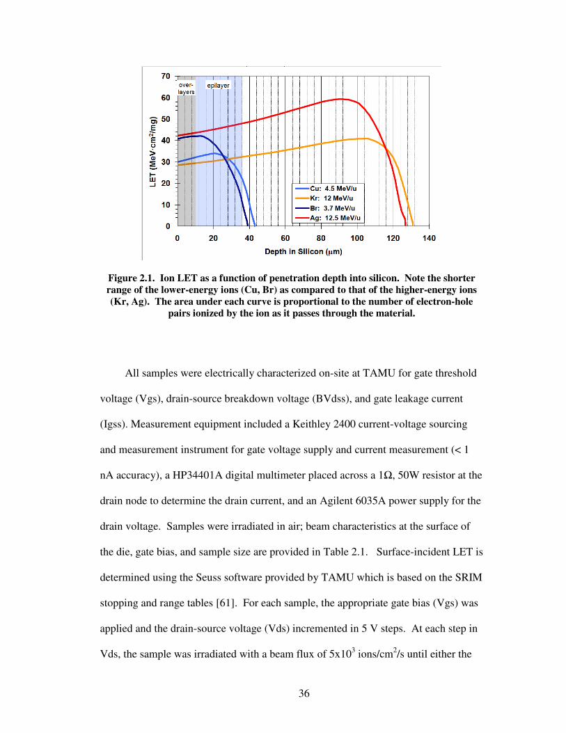
36
Figure 2.1. Ion LET as a function of penetration depth into silicon. Note the shorter
range of the lower-energy ions (Cu, Br) as compared to that of the higher-energy ions
(Kr, Ag). The area under each curve is proportional to the number of electron-hole
pairs ionized by the ion as it passes through the material.
All samples were electrically characterized on-site at TAMU for gate threshold
voltage (Vgs), drain-source breakdown voltage (BVdss), and gate leakage current
(Igss). Measurement equipment included a Keithley 2400 current-voltage sourcing
and measurement instrument for gate voltage supply and current measurement (< 1
nA accuracy), a HP34401A digital multimeter placed across a 1Ω, 50W resistor at the
drain node to determine the drain current, and an Agilent 6035A power supply for the
drain voltage. Samples were irradiated in air; beam characteristics at the surface of
the die, gate bias, and sample size are provided in Table 2.1. Surface-incident LET is
determined using the Seuss software provided by TAMU which is based on the SRIM
stopping and range tables [61]. For each sample, the appropriate gate bias (Vgs) was
applied and the drain-source voltage (Vds) incremented in 5 V steps. At each step in
Vds, the sample was irradiated with a beam flux of 5x10³ ions/cm2/s until either the
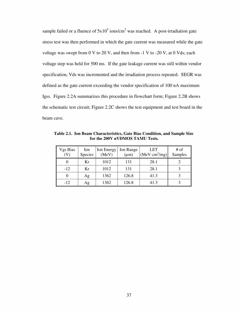
37
sample failed or a fluence of 5x10⁵ ions/cm2 was reached. A post-irradiation gate
stress test was then performed in which the gate current was measured while the gate
voltage was swept from 0 V to 20 V, and then from -1 V to -20 V, at 0 Vds; each
voltage step was held for 500 ms. If the gate leakage current was still within vendor
specification, Vds was incremented and the irradiation process repeated. SEGR was
defined as the gate current exceeding the vendor specification of 100 nA maximum
Igss. Figure 2.2A summarizes this procedure in flowchart form; Figure 2.2B shows
the schematic test circuit; Figure 2.2C shows the test equipment and test board in the
beam cave.
Table 2.1. Ion Beam Characteristics, Gate Bias Condition, and Sample Size
for the 200V nVDMOS TAMU Tests.
Vgs Bias (V)
Ion Species
Ion Energy (MeV)
Ion Range (µm)
LET (MeV·cm2/mg)
# of Samples
0 Kr 1012 131 28.1 2
-12 Kr 1012 131 28.1 3
0 Ag 1362 126.8 41.3 3
-12 Ag 1362 126.8 41.3 3
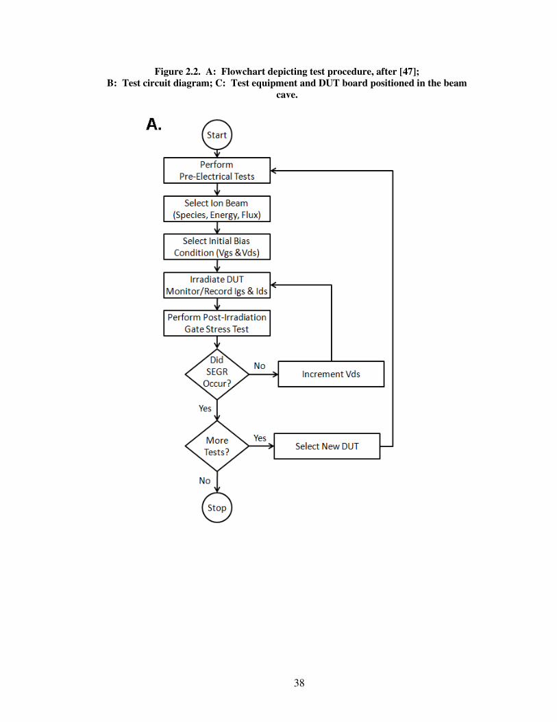
38
Figure 2.2. A: Flowchart depicting test procedure, after [47];
B: Test circuit diagram; C: Test equipment and DUT board positioned in the beam
cave.
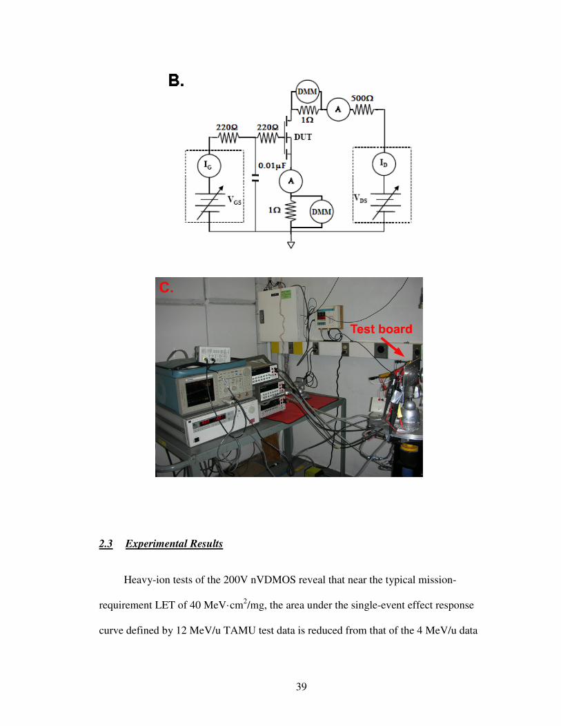
39
2.3 Experimental Results
Heavy-ion tests of the 200V nVDMOS reveal that near the typical mission-
requirement LET of 40 MeV·cm2/mg, the area under the single-event effect response
curve defined by 12 MeV/u TAMU test data is reduced from that of the 4 MeV/u data

40
provided in the vendor datasheet (Figure 2.3). This finding is in keeping with prior
studies of energy effects on SEGR susceptibility in power MOSFETs [49]. For the
lower surface-incident LET of 28 MeV·cm2/mg, the SEE response curves defined by
4 MeV/u Cu and 12 MeV/u Kr are comparable, though the -12 Vgs Kr data suggest a
faster roll-off of the SEE response curve than is detectable with the vendor Cu data
set.
When typical derating factors of 0.75 Vds and 0.6 Vgs are applied to the
vendor’s 41 MeV·cm2/mg data (Figure 2.3), the 12 MeV/u Ag data at 0 Vgs fall just
above the derated 4 MeV/u Br SEE response curve, leaving no margin for factors
such as part-to-part variability. Two important questions remain: Is additional
margin required to avoid SEGR on orbit from higher energy, heavier ions, and if so,
does standard derating of the higher-energy test data provide a safe margin to avoid
SEGR from these more energetic, heavier ions found in space but unavailable for
evaluation at typical accelerator facilities? To answer these questions, simulations of
SEGR must be performed.

41
Figure 2.3. Single-event effect response curves for the 200V nVDMOS showing energy
dependence at the higher LET. Y-error bars show measurement uncertainty. Derated
Br curve is indicated by the purple dotted line; derating factors = 0.75 Vds and 0.6 Vgs.
2.4 Simulation Methods
The general-purpose technology computer-aided design (TCAD) device
simulator, Synopsys Sentaurus Device [59], is used to perform transient simulations
of SEGR. For the 200V radiation-hardened nVDMOS, the transistor structure is
developed using standard doping and geometry profiles for a medium-voltage device
as determined from the literature [2, 4], and is calibrated to the SEE response curve
for 4 MeV/u heavy-ion accelerator beam data provided in the vendor datasheet. In
addition, a 500V commercial pVDMOS TCAD model is developed from a subsection
of existing 25 MeV/u TAMU data and scanning electron microscope images provided
in a NAVSEA-Crane radiation test report [60]. Small adjustments in the geometry

42
and doping were made to calibrate the models, whereby the doping was adjusted to
achieve the appropriate reverse-bias breakdown voltage, BVdss, and the neck width
and body diffusion depth were adjusted to fit the SEGR test data. A brief analysis of
the impact of adjustments to the drain neck width and epilayer doping concentration
is given in Appendix A. Figure 2.4 depicts the geometries and doping profiles of the
200V and 500V VDMOS models simulated. Three-dimensional simulation fidelity
was obtained using a 2-dimensional cylindrical coordinate system since all ions were
simulated to strike at the center of the drain neck region at normal incidence.
Figure 2.4. Simulated VDMOS models: Cylindrical coordinates are used such that the
images depicted here are of one radial slice of the full model. “X” is the radial
coordinate and the middle of the drain neck region lies at X= 0 µµµµm; “Y” is the axial
coordinate. A: 200V nVDMOS model; B: 500V pVDMOS model.
43
The device simulator solves the Poisson, charge-continuity, and current
equations in the silicon using finite-element techniques. Simulated ion strikes reflect
the changing ionizing energy loss along the length of the ion track as calculated with
the SRIM stopping power and range tables [61]. A Gaussian radial distribution with
characteristic radius of 50 nm is used until the actual track radius determined from the
Fageeha model [62] falls below 50 nm; this calculated radius is then substituted. The
Fageeha model determines the electron-hole pair density as a function of distance
from the track core based upon the energy loss due to ionized delta electrons traveling
in the radial direction. For the thicker 500V device, the finite time for the ion to pass
through the silicon is accounted for by widening of the track radius into a conical
shape as follows. The time for the ion to pass through the modeled device was
approximated by calculating the ion velocity from its incident energy, then
multiplying the inverse of this velocity by the thickness of the modeled silicon region.
Transient simulations were then performed with a uniform characteristic radius of 50
nm. The hole density near the silicon-silicon dioxide interface was plotted as a
function of distance from the ion track core both at the time of the ion strike and at
the calculated time for the ion to pass through the modeled device. The difference in
the distance at which the hole density reached its background level was then used as
the ion-specific track characteristic radius at the Si/SiO2 interface. This characteristic
radius was linearly reduced to 50 nm at the end of its passage through the silicon.
The physics models governing charge transport are limited to those built into
the simulator; for this study, they included concentration-dependent Shockley-Read-
Hall and Auger recombination; bandgap narrowing and Fermi-Dirac statistics;

44
velocity saturation and impact ionization driven by the gradient of the quasi-Fermi
levels; and impurity and carrier-carrier scattering. Determination of SEGR was made
from the simulated transient peak electric field across the oxide using the Titus-
Wheatley semi-empirical expression for the critical field for breakdown (Ecrit) based
upon the ion atomic number (Z) as given in (3) in section 1.4.2 above. Electrical
stress measurements of the pristine oxide cannot be used since the interaction of the
heavy ion with the oxide reduces Ecrit [30, 36, 63]. This expression yielded
reasonable agreement between simulated and experimental SEGR data for a single
ion species in a previous study by Titus, et al. [46]. We conducted experiments to
validate the use of this expression in our work; these results are presented in chapter
3.
2.5 Simulation Results
2.5.1 200V Radiation-Hardened nVDMOS
Simulation studies were performed to evaluate whether typical derating of
heavy-ion accelerator test data will bound the risk of SEGR on-orbit. As shown in
Figure 2.5, the model of the 200V radiation-hardened nVDMOS was successfully
calibrated to the vendor’s copper and bromine data. In this figure and subsequent
SEE response curve plots, error bars on experimental data reflect measurement
uncertainty, and simulation error bars reflect the uncertainty in the oxide field
required for SEGR. Without any changes to the extracted geometry and doping of the
device structure, simulations of the silver and krypton strikes predicted the higher-

45
energy experimental silver and krypton data taken in this study (Figure 2.6),
demonstrating the predictive capability of the method.
Figure 2.5. Successful calibration of 200V model to 4 MeV/u vendor data.
Figure 2.6. 200V nVDMOS model predicts 12 MeV/u TAMU data.

46
The ion species used to develop the Titus-Wheatley expression (3) range from
Z=28 (Ni) to Z=79 (Au). With this expression, the SEE response curve for ions up to
Z=79 can therefore be extrapolated from the model. Figure 2.7 plots the simulation
results of 68 MeV/u Au, showing that the SEE response curve for Au ions with a
surface-incident LET of 40 MeV·cm2/mg lies inside the SOA defined by derating the
lower-energy bromine data (purple dotted line). Application of a 0.75 Vds derating
factor to these lower energy data would therefore result in some risk for SEGR
occurring on orbit. Conversely, when this same derating factor is applied to the
higher-energy silver data (red dash-dot line), the simulated SEE response curve for
Au ions falls just outside the resulting SOA. Operating within the SOA defined from
derating the higher-energy TAMU data may therefore prevent SEGR for ions as
heavy as Au, although there is minimal margin for other variables such as part-to-part
variability and aging effects. A 0.75 derating factor applied to the SEE response
curve defined by 12 MeV/u data is appropriate for this device when the low relative
flux of heavier species is considered.
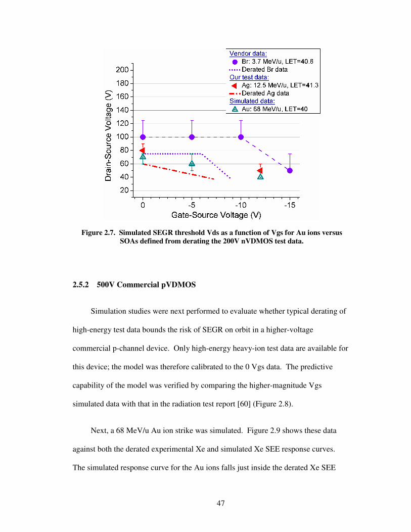
47
Figure 2.7. Simulated SEGR threshold Vds as a function of Vgs for Au ions versus
SOAs defined from derating the 200V nVDMOS test data.
2.5.2 500V Commercial pVDMOS
Simulation studies were next performed to evaluate whether typical derating of
high-energy test data bounds the risk of SEGR on orbit in a higher-voltage
commercial p-channel device. Only high-energy heavy-ion test data are available for
this device; the model was therefore calibrated to the 0 Vgs data. The predictive
capability of the model was verified by comparing the higher-magnitude Vgs
simulated data with that in the radiation test report [60] (Figure 2.8).
Next, a 68 MeV/u Au ion strike was simulated. Figure 2.9 shows these data
against both the derated experimental Xe and simulated Xe SEE response curves.
The simulated response curve for the Au ions falls just inside the derated Xe SEE

48
response curves. A 0.75 derating factor applied to the SEE response curve defined by
21 MeV/u test data therefore does not bound the risk of SEGR from 40 MeV·cm2/mg
(surface-LET) ions for this device.
Figure 2.8. Single-event effect response curves for the 500V pVDMOS showing
good agreement between simulated and test data.

49
Figure 2.9. Simulated SEGR threshold Vds as a function of Vgs for simulated Au ion
strikes versus 0.75 derating factor applied to test and simulated SEE response curves
for the 500V pVDMOS. The SOA is defined as the region above the derated curves (the
region of lower-magnitude drain biases above either the brown dotted or green dot-
dash line).
2.6 Discussion
Most mission requirements for SEGR avoidance are specified in terms of ion
incident LET; however, for thick-epilayer vertical power MOSFETs the off-state bias
SEE response curve is a function of both ion energy and species [49, 51]. SEGR may
occur when a heavy ion passes through the drain neck region; normally-incident ions
pose the greatest risk. For a given surface-incident LET, higher-energy ions will
penetrate deeper into the epilayer, resulting in greater charge ionization in this
sensitive volume (Figure 2.1). Charge separation in the vertical drift field produces a
transient high field across the gate oxide (Figure 1.4). The electric field required to

50
rupture the oxide is lowered by the passage of the ion through the oxide; this critical
field is primarily a function of ion species [41]. As expected, for a typical mission-
requirement LET, higher-energy heavy-ion test data taken in this study resulted in a
reduced area under the SEE response curve as compared with that from lower-energy
test data (Figure 2.3).
TCAD simulation studies were performed with 68 MeV/u Au having the
common mission surface-LET threshold requirement of 40 MeV·cm2/mg. Gold ions
at this energy are unavailable for testing at typical accelerator facilities, but constitute
a portion of the GCR flux in space. This simulation therefore evaluated whether
derating of higher-energy TAMU data will bound the risk of SEGR on-orbit.
Simulation results suggest that operating the radiation-hardened 200V nVDMOS
within the SOA defined from derating the higher-energy TAMU data may prevent
SEGR for ions as heavy as Au for a mission-requirement LET threshold of 40
MeV·cm2/mg (Figure 2.7). This finding suggests that the typical 0.75 derating factor
for the drain voltage is appropriate for this device, with the margin being consumed
chiefly by these energy and species effects.
The TCAD model of the commercial 500V pVDMOS reveals that the simulated
SEE response curve for 68 MeV/u Au ions falls just inside the SOA defined from the
derated 21 MeV/u Xe test data (Figure 2.9). This result suggests that for this high-
voltage device, a 0.75 derating factor applied to TAMU test data does not fully bound
the on-orbit risk of SEGR from heavy ions with an incident LET of 40 MeV·cm2/mg.
51
An important outcome of this study is the demonstration of the capability and
usefulness of TCAD models for augmenting SEGR data from accelerator beam
facilities. SEGR testing at these facilities is very expensive due to its destructive
nature, and is limited to a small subset of ion species and energies. Successful
calibration and development of predictive models required minimal test data: In the
case of the radiation-hardened device, the low-energy vendor data sufficed; for the
commercial device with no vendor heavy-ion test data, ion-beam data at a single Vgs
and two incident LETs sufficed.
The calibrated and predictive models developed in this study provide support
for the Titus-Wheatley expression given in (3) in which the ion atomic number, as
opposed to LET, is the important parameter for determining the electric field needed
to rupture the oxide. Rupture occurs when the sum of the field due to the applied Vgs
and the transient field generated by the epilayer response to an ion strike exceeds this
critical field. Calibration of the models in this study to accelerator-beam test data was
achievable with the use of this expression.
2.7 Conclusion
A simulation-based methodology has been demonstrated to examine whether
typical derating of high-energy heavy-ion accelerator test data bounds the risk for
SEGR for the much higher-energy space environment. This work is to our
knowledge the first to examine the appropriateness of the current derating method.
To this end, the SEGR susceptibility of two very different VDMOS devices (a 500V
commercial p-type and a 200V radiation hardened n-type) was modeled. This work
52
suggests that the typical derating factor of 0.75 applied to a SEE response curve
developed with high-energy test data provides reasonable on-orbit hardness
assurance, although in the higher-voltage pVDMOS, it did not bound the risk of
failure.
The simulation methodology demonstrated here may only require low-energy
accelerator test data for model calibration. These models may be used to generate
multiple SEE response curves to examine the sensitivity of the device to changes in
ion species and energy, enhancing assurance of on-orbit success without the expense
of testing at ultra-high energy facilities.
The methodology we developed here for assessing appropriate derating levels
can be summarized as follows. First, obtain or take test data: these data ideally
should include ions with the mission requirement surface-incident LET, having
appropriate energies to fully penetrate the device epilayer. Barring this ideal data set,
a device structure can be calibrated to any data set comprising two ion species or
incident LETs. Second, apply the standard derating factors to the SEE response curve
formed by the data. Third, simulate the expected worst-case ion species and energy
for the mission orbit environment. A decision then can be made: do the simulated
worst-case data fall inside or outside the safe-operating area defined by the standard
derating factors? The derating factor can then be adjusted accordingly. In this way,
mission risk can be decreased and the usable portion of a power MOSFET’s voltage-
blocking capability can be maximized, reducing the costs associated with using
higher-voltage devices to accommodate overly-conservative derating.

53
Finally, we note that the relative importance of the ion species and ion energy in
inducing SEGR is still uncertain, limiting our ability to identify if or when a heavier
ion species with a lower LET will be more likely to induce SEGR than a lighter
species with a higher LET. Modeling and careful experimental validation will help to
define these boundaries, enabling improved SEGR rate estimations. We pursue this
analysis in the next chapter.
54
Chapter 3: Studies of Ion Species Effects in SEGR Susceptibility of
Power MOSFETs
3.1 Motivation
In this chapter, we focus on the effect of the ion atomic number on SEGR
susceptibility. As described in section 1.4.2, the mechanisms of SEGR involve both
the heavy ion’s interaction with the gate oxide and the charge it ionizes in the
epitaxial layer of the device. More specifically, SEGR is attributable to the following
processes: 1) The passage of the ion through the gate oxide temporarily reduces the
electric field required for dielectric breakdown; 2) the ionized charge within the
epilayer collapses the depletion region, allowing a greater portion of the high off-state
drain voltage to fall across the gate oxide. Given these mechanisms, we will: 1)
validate the method of chapter 2 for determining SEGR in simulations where we used
a semi-empirical approach to define the critical field for gate rupture; and 2) assess
the relative importance of the gate oxide response mechanism for SEGR.
We show through simulation that the gate oxide field for rupture can be
experimentally isolated by shorting to ground the drain and source/body contacts, and
hence is a valid approach for defining this critical field for simulation purposes. The
semi-empirical formula relied upon in chapter 2 to identify this critical field was
developed by Titus, et al., [41] using this method, and here we confirm
experimentally that this formula is valid for the 200V device we modeled. We

55
attempt to complement these studies using two-photon absorption laser tests to
examine SEGR susceptibility in the absence of this oxide response mechanism.
Finally, we conduct experiments that strongly suggest that the ion interaction with the
silicon dioxide reduces the gate breakdown voltage even at non-zero drain-source
biases. This study demonstrates that this oxide response mechanism is important and
should not be ignored in approaches to SEGR hardness assurance. In addition, our
work supports that this oxide response mechanism is a function of the striking ion’s
atomic number as opposed to its LET. In the final chapter of this dissertation, we
discuss possible mechanisms for this ion species dependency.
3.2 Verification of the Titus-Wheatley Formula of the Critical Oxide Electric
Field for SEGR
The SEGR simulations we performed in chapter 2 rely heavily on the Titus-
Wheatley formula [41] (equation (3), chapter 1) to determine whether the simulated
peak electric field across the silicon dioxide is sufficient to rupture the gate. This
formula is repeated here for convenience to the reader:
)44/Z1()t)(10(V ox
7
gs +=crit (4)
where tox is the oxide thickness in cm, 107 reflects the pristine silicon dioxide
breakdown strength (V/cm), and Z is the atomic number of the heavy ion. Electrical
stress measurements of the breakdown of an unirradiated oxide cannot be used since
the interaction of the heavy ion with the oxide reduces the critical field for rupture
[30, 36, 63]. In this section, this formula is experimentally validated for the 200V
power MOSFET simulated in chapter 2; then, in section 3.3, we will show that the

56
methods used to experimentally isolate the oxide field from the epilayer response are
valid.
3.2.1 Experimental Methods
The radiation-hardened 200V n-type vertical power MOSFET (VDMOS)
studied in chapter 2 was used for the following experiments. Samples came from two
wafers from the same lot. Heavy-ion test data were taken at the Texas A&M
University Cyclotron Facility (TAMU). All samples were fully electrically
characterized off-site; on-site prior to irradiation, a gate stress test was performed
prior to irradiation in which the gate leakage current was measured as a function of
gate voltage at 0 Vds bias. Measurement equipment included a Keithley 2400
current-voltage sourcing and measurement instrument (SMU) for gate voltage supply
and current measurement (< 1 nA accuracy) and either a Keithley 2400 or 2410 SMU
for the drain voltage supply and drain current measurement. Samples were irradiated
in air at normal incidence. For each sample, the capacitor response [41] of the device
was investigated by holding the drain-source bias at 0 V, isolating the oxide field
from ion effects in the epilayer. A strong negative gate bias (Vgs) of higher
magnitude than the gate bias rating was applied and incremented in -0.5 V steps until
sample failure. At each step in Vgs, the sample was irradiated with a beam flux in the
range of 5x10³ ions/cm2/s to 2x10⁴ ions/cm2/s, until either the sample failed or a
fluence of 3x10⁵ ions/cm2 was reached. Six different combinations of ion species and
energies were used (see Table 3.1 in section 3.2.2). Failure was defined by a sudden
increase in gate leakage current to the SMU supply limit. Figure 3.1A summarizes
the test procedure in flowchart form; Figure 3.1B shows the schematic test circuit;

57
Figure 3.1C shows the operator control room at TAMU with SMUs, computer
interfaces, and DUT switchbox; and Figure 3.1D shows the individually-selectable
devices mounted on the test board with a single DUT positioned in the ion beam.
Figure 3.1. A: Flowchart depicting test procedure, after [47]. Note the absence of a
post-irradiation gate stress test due to the high-magnitude Vgs bias conditions during
irradiation. B: Test circuit diagram. C. TAMU operator control room with test
equipment. D. Test board with DUT in line with beam.

58

59
3.2.2 Results
The results imply that the oxide field for gate rupture is reduced as a function of
the ion species. In this experiment, we found the gate bias required for gate rupture
under 0 Vds bias for six different combinations of ion species and energies. In all
cases, gate rupture occurred during irradiation, resulting in a sudden gate leakage
current increase to the 1 mA supply current limit. Results are summarized in Table
3.1 where for each sample tested, the last passing gate bias and the bias at failure are
given as a function of ion beam species, energy, and LET at the surface of the die.
For comparison, the applied gate bias required to rupture the gate oxide in the
absence of any irradiation is given at the bottom of this table.
Table 3.1. Heavy-Ion Test Results of the Critical Gate Voltage
for SEGR as a Function of Ion Species and Energy
Ion Beam Characteristics Results Species Energy LET Range Sample Last Passing Vgs Vgs at Failure
Z MeV MeV·cm2/mg µm S/N V V
29 422 25.8 64.5 1W13 -52.5 -53 29 422 25.8 64.5 2W13 -51.5 -52 29 825 18.5 145.4 19W23 -53.5 -54 29 825 18.5 145.4 20W23 n/a -52.5 36 1089 27.7 140.4 2W23 -48.5 -49 36 1089 27.7 140.4 3W23 -49 -49.5 47 740 53.7 64.3 8W13 -42 -42.5 47 740 53.7 64.3 9W13 -42 -42.5 47 740 53.7 64.3 8W23 -41 -41.5 47 1405 42.5 124.8 14W13 -43 -43.5 47 1405 42.5 124.8 15W13 -43.5 -44 47 1405 42.5 124.8 26W23 -44 -44.5 54 1618 54.6 119.0 11W23 -38.5 -39 54 1618 54.6 119.0 12W23 -40 -40.5 54 1618 54.6 119.0 13W23 -40.5 -41 0* n/a n/a n/a Lot test n/a -67 ± 4
* Electrical breakdown voltage for unirradiated samples.

60
The critical voltage for gate rupture is plotted as a function of ion species (red
diamonds, Figure 3.2). These data are fitted (red dot-dash line, Figure 3.2) with a
two-parameter reciprocal function of the form y=A/(1+Bx); this non-linear function
yields a better fit than a simple linear function or a power-law model according to the
adjusted R2 value (0.9671 versus 0.9658 or 0.9627, respectively). The R2 value gives
the fraction of the variability in the data not captured by the model used to fit the data.
Its value therefore ranges from 0.0 to 1.0, demonstrating the goodness of fit. The
adjusted R2 accounts for the degrees of freedom in the model, since the R2 value will
increase simply due to the addition of model parameters [64]. Notably, the best-
fitting model to our data is the form of the Titus-Wheatley formula (4), and for these
data results in the following fitted function:
)5.49Z(1-84 Vcrit += (5)
Comparing the numerator in (5) to its analogue in (4), this fit suggests a gate oxide
thickness of 84 nm. Since this value is too low, we fix the second parameter, B, to
1/44, that of the Titus-Wheatley formula; we then find the numerator yielding the best
fit to our data. This fit, shown as a blue dotted line in Figure 3.2, yields an accurate
thickness for this device. Fixing the second parameter to 1/44 reduces the adjusted R2
value only minimally, from 0.9671 to 0.9650.

61
Figure 3.2. Critical Vgs for SEGR as a function of ion species. Data are fitted to the
two-parameter reciprocal function y=A/(1+Bx), with either both parameters free, or
with B fixed to that of the Titus-Wheatley formula (4). The fits are plotted for the full
range of Z values over which the Titus-Wheatley formula is valid.
3.2.3 Implication for Simulation Methods of SEGR Prediction
We examined the legitimacy of using the Titus-Wheatley formula (4) as a
criterion for the occurrence of SEGR in TCAD simulations of ion strikes to VDMOS
structures by performing a set of experiments on the 200V nVDMOS simulated in
chapter 2. It is not possible to experimentally measure the electric field across the
gate oxide that leads to gate rupture. We instead attempted to isolate the gate oxide
field by grounding the drain to the source, and measured the applied gate-source
voltage under which SEGR occurs during irradiation by heavy ions of differing
species and energies. We show that when we fit these data with a function in the

62
form of the Titus-Wheatley formula, holding the second parameter fixed at 1/44 and
leaving the numerator as a free fitting parameter, the best fit agrees with the gate
oxide thickness as indicated by the manufacturer. This validation of the Titus-
Wheatley formula suggests that in our device simulation work, we can use this
expression to identify the critical electric field that must develop across the gate oxide
for gate rupture to occur (taking Vcrit in (4) and dividing by the oxide thickness).
The ion species simulated, Vgs applied, and gate-oxide thickness modeled are
therefore sufficient for identifying when the simulation results indicate SEGR.
3.3 Validation of the Experimental Method to Isolate the Critical Oxide Field for
Gate Rupture
A key assumption of the Titus-Wheatley formula and its use in SEGR
simulations is that the critical field that must develop across the oxide is modulated
by the ion species interaction with the oxide, and not from a change in potential at the
silicon-silicon dioxide interface due to the ion passage through the silicon. If the
latter case were true, we could no longer decouple the oxide response from the silicon
response to an ion strike simply by setting Vds = 0 V. Important to this work, we
could not assume that the critical oxide electric field for SEGR remains the same
when varying Vds. Allenspach, et al., [31] performed simulation studies
demonstrating that at 0 Vds, the field across the oxide remained at the value of
Vgsapplied/tox following strikes by ion species ranging from silicon (Z = 28) to gold (Z
= 79). In all cases, the simulated gate bias was held at the empirically-determined
critical value for SEGR for the given ion species. In this study, we validate these
findings, exploring them in more detail. We apply a constant Vgs and simulate an ion

63
strike for which that Vgs is the critical threshold bias for SEGR, as well as an ion
strike whose critical threshold Vgs is much less than the simulated applied bias. In
this way, we compare the effects of two different ionization energies in the epilayer
on the resulting oxide field. We then compare the simulation results with our
empirical data from section 3.2, demonstrating that the critical electric field as
defined by the Titus-Wheatley formula is primarily the isolated oxide field.
3.3.1 Simulation Methods
Studies of the oxide electric field were performed using the model of the 200V
nVDMOS described in chapter 2, with the oxide thickness reduced from 100 nm to
the 89 nm suggested in our previous study (section 3.2). Here, all device simulations
were performed with 0 Vds and -50 Vgs boundary conditions. Both transient 1089
MeV krypton (surface-incident LET = 27.7 MeV·cm2/mg, Z = 36) and 2482 MeV
gold (surface-incident LET = 81.4 MeV·cm2/mg, Z = 79) ion strikes were simulated.
As in chapter 2, these simulations incorporated the changing ionizing energy loss
along the length of the ion track as determined from stopping power tables generated
with the Monte Carlo code, SRIM [61], and a Gaussian radial distribution with a
uniform characteristic radius of 50 nm.
3.3.2 Results
The results show that the field across the oxide remains essentially the same
before and during an ion strike when Vds is held at 0 V. More specifically, the field
in the silicon epilayer below the oxide is reduced, shifting this small change in field to
the oxide region, whose field rises by about 1%. Figure 3.3 is a close-up of the

64
epilayer-oxide interface showing this change in the fields. The left and right panels
are prior to the Au ion strike and at the time that the transient peak in the oxide field
occurs after the ion strike, respectively. The details of our simulation results are as
follows. When a high-magnitude off-state gate bias of -50 V is applied with Vds held
at 0 V, the hole concentration in the lightly-doped n-type drain epilayer at the Si/SiO2
interface is elevated to 8x10¹⁸ /cm3 due to the strong negative bias on the gate contact.
This density is 13 orders of magnitude above the background hole density of 4x10⁵
/cm3. This inversion layer extends the built-in potential in the p-well along the
Si/SiO2 interface. When the ion strikes, this distribution of charge is disrupted by the
generation of high concentrations of electrons and holes along the ion track. This
change in charge concentration deforms the prestrike electrostatic potential, shifting
more of the voltage drop between gate and drain across the gate oxide as the epilayer
becomes more conductive. As a result, a very small transient rise in the electric field
in the gate oxide occurs, raising this field toward the ideal Vgsapplied/tox value. This
process can be seen in the contour plots in Figure 3.4 of the electric field, electrostatic
potential, and electron and hole densities at various time steps during the simulation
of the gold ion strike.

65
Figure 3.3. Electric field in the gate oxide and silicon epilayer beneath prior to a Au-ion
strike (left) and at 20 ps following the strike (right) – the time at which the maximum
change in the oxide field occurred. The oxide/silicon interface is at Y= 0 µµµµm. The
legend for the electric-field contours applies to both panels. See Figure 3.4 below for
images of the complete half-cell model.
Figure 3.4 (on following pages). Effects of Au ion strike at 0 Vds and -50 Vgs on:
A. Electric field; B-C. Electrostatic potential; D. Electron density; and E. Hole density.
Time elapsed: 1) prestrike; 2) 2 ps; 3) 20 ps (time of maximum transient electric field);
4) 1 ns.

66

67

68
The maximum change in electric field occurs in the oxide at the core of the ion
track. The magnitude of change is a function of the amount of charge ionized along
the ion track, and hence the track conductivity. The magnitude of the electric field
and its change at several time steps are listed in Table 3.2. Figure 3.5 shows the
electric field in the oxide as a function of time, for the gold and krypton ion strikes.
As can be seen from the table and Figure 3.5, at the center of the krypton ion track the
peak oxide electric field changes by 45.8 kV/cm, corresponding to the change in
potential at the Si/SiO2 interface from -0.524 V to -0.116 V. In the simulations of a
2482 MeV Au ion strike under the same -50 Vgs bias, the potential at the center of
the ion track at the interface rose from -0.524 V to 0.060 V. In both cases, only about
a 1% change in the oxide field occurs.

69
Table 3.2. Oxide Electric Field Effects Following a Kr or Au Ion Strike at -50 Vgs
and 0 Vds
Ion LET at Oxide (MeV·cm
2/mg)
Time (ps)
Eox (V/cm)
∆ Eox (V/cm)
-- -- prestrike 5.55909 x10⁶ --
Kr 28.1 2 5.59926 x10⁶ 40,170
18 5.60419 x10⁶ 45,810 750 5.58527 x10⁶ 26,180
Au 82.2 2 5.61368 x10⁶ 54,590
20 5.62473 x10⁶ 65,640 1,100 5.59975 x10⁶ 40,660
Figure 3.5. Oxide electric field as a function of time, under -50 Vgs and 0 Vds bias at
the center of the drain neck region at the core of the ion track. Note the very small y-
axis range: The transients are 1% or less of the prestrike oxide electric field of
5.559x10⁶ V/cm.

70
3.3.3 Discussion
These transient simulations strongly suggest that the passage of the ion through
the oxide lowers the critical field for rupture as compared to the critical field for
electrical breakdown. Biasing a VDMOS with 0 Vds and a high-magnitude non-zero
Vgs is an effective way to isolate this oxide response during heavy-ion irradiation.
These simulations further suggest that the relationship between the threshold gate-
source voltage for SEGR at 0 Vds and the ion species, as given by the Titus-Wheatley
formula (4) is governed by the physics of the ion interaction with the oxide itself, and
depends minimally on the effects of ionized charge in the silicon epilayer. In the
simulations, the charge ionized in the silicon epilayer contributed less than 1 V/tox to
the maximum gate oxide electric field when the drain was biased at 0 V. In
comparison, the applied gate bias was -50 V. More notably, for this device, the
experimental difference in threshold Vgs biases for SEGR at 0 Vds for krypton versus
gold, as shown in Figure 3.2, is extrapolated to be 16 V, whereas the difference in the
peak surface potentials in the simulations of these krypton and gold ions is only 0.176
V. The minimal change in oxide field due to the charge ionized in the epilayer
clearly cannot account for the ion species effects on the gate oxide breakdown voltage
shown in our experiments in section 3.2.
We may assume that at 0 Vds, the rupture could occur anywhere along the gate
oxide, no longer favoring the drain neck region; however, failure analyses of other
nVDMOS devices reveal ruptures in the oxide above the center of the drain neck
region [65]. This finding may be a result of the small contribution to the field from
the ionized charge in the epilayer identified in this study, given that the maximum

71
field transient occurs for ion strikes at the center of the drain neck region where the
lateral field near the oxide/epilayer interface is smallest.
3.4 Two-Photon Absorption Laser Tests to Reveal the Criticality of Gate-Oxide
Damage for SEGR
3.4.1 Purpose
We have verified that we can isolate the oxide response to a heavy-ion strike
from the epilayer response by biasing the drain at 0 Vds. Unfortunately, it is not
feasible to assess the epilayer response in the absence of heavy-ion interaction with
the oxide. Backside irradiations, in which the heavy ion penetrates the die at the
drain surface, cannot be controlled to permit ion passage through the majority of the
epilayer without also potentially penetrating the oxide. This problem is due to energy
straggle, whereby the actual path length for a given single ion varies due to the
randomness of the collisions and due to amplification of any initial energy spread in
the beam itself. This amplification arises from the non-linearity of the stopping
powers as a function of energy [61]. A possible alternative to heavy-ion testing is the
use of two-photon absorption (TPA) laser testing, which ionizes charge in the silicon
but cannot ionize charge in the silicon dioxide.
As a complement to heavy-ion testing for single-event effects, TPA laser tests
may be used to control the location of charge ionization within the silicon, permitting
a mapping of the epilayer response for a given bias condition. TPA involves the use
of a laser wavelength less than the bandgap of silicon. The theory of this method and
its application in single-event effect testing can be found in [66]. At high light

72
intensities, a single electron-hole pair can be generated by the simultaneous
absorption of two photons. In this way, the laser can be focused such that the beam
can pass through the silicon with minimal attenuation (depending on the doping
concentration), but yield substantial charge generation at the focal point where the
intensity is highest. Charge generation by TPA is proportional to the square of the
laser pulse intensity, such that the charge density falls off rapidly outside the focal
area. An important characteristic of TPA laser testing is that no light is absorbed by
the silicon dioxide, so that no charge is generated in this region. In this way, TPA is a
useful tool for determining whether oxide damage is a necessary component for
SEGR to occur, or whether the transient increase in the oxide field due to charge
ionized in the epilayer collapsing the depletion region is sufficient for rupture. In
addition, it may be possible to map the relative importance of the locations in which
charge is ionized and verify the lesser importance of charge ionized in the drain
substrate region.
3.4.2 Sample Preparation and Experimental Methods
We performed TPA studies on specially-prepared 200 V power MOSFETs, in
collaboration with International Rectifier Corporation (IR). The laser cannot
penetrate metal layers, so that top-side irradiation of the gate neck region is not
possible. The samples were therefore prepared by IR for backside irradiation in the
same manner as detailed in [67] and briefly described here. Recall that the vertical
power MOSFET structure has the drain metal contact along the bottom of the die.
This metal contact was ground away, and the heavily-doped substrate thinned to
about 60 µm. This thinning was necessary because the TPA laser light can be
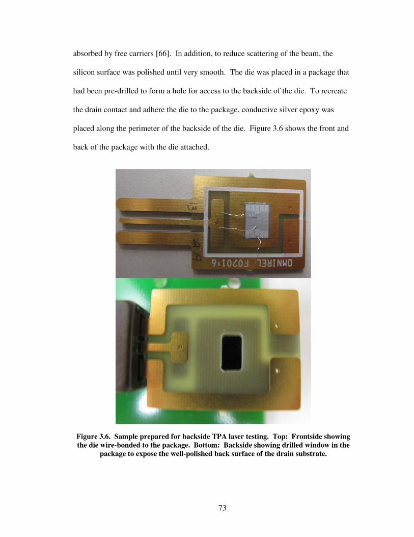
73
absorbed by free carriers [66]. In addition, to reduce scattering of the beam, the
silicon surface was polished until very smooth. The die was placed in a package that
had been pre-drilled to form a hole for access to the backside of the die. To recreate
the drain contact and adhere the die to the package, conductive silver epoxy was
placed along the perimeter of the backside of the die. Figure 3.6 shows the front and
back of the package with the die attached.
Figure 3.6. Sample prepared for backside TPA laser testing. Top: Frontside showing
the die wire-bonded to the package. Bottom: Backside showing drilled window in the
package to expose the well-polished back surface of the drain substrate.

74
Tests were performed at the Naval Research Laboratory. The test setup is
similar to that for heavy-ion testing. Figure 3.7 shows the laser test board and
diagram. Two Keithley 2400 source-measuring units supplied the gate and drain
biases and measured currents, which were recorded at 100 ms intervals. A Tektronix
CT-2 current transformer was connected to an oscilloscope set to trigger on current
transients during laser irradiation.
Figure 3.7. Laser test board with sample mounted (top). Board is placed on a stage
beneath a 100X microscope objective used to focus the laser beam. Circuit diagram for
the test board is shown at the bottom.

75
The sample was mounted on the test board and attached to a stage with x-y-z
movement precision of 0.1 µm. The vertical positioning controlled the depth of the
focal area of the beam in the sample. The highly-doped body and source regions
showed as dark regions, whereas the neck region was whiter. In this way, the focal
area could be placed in the center of the drain neck region at varying depths below the
oxide/silicon interface. The area of the focal region defined by the 1/e light intensity
boundary forms an ellipsoid, with the long axis aligned along the depth (z-axis) of the
sample. This long axis extends approximately 10 µm in diameter, with the narrower
ellipsoid axes having approximately a 1.6 µm diameter. The laser was set to
maximum energy of 25-30 nJ. The wavelength of the laser beam was 1260 nm.
Single laser pulses having a 120 fs pulse width were delivered using a shuttering
mechanism.
3.4.3 Results
We did not succeed in rupturing the gate of our samples at biases below the
electrical gate breakdown voltage. The center of the laser focal area was positioned
at the silicon/silicon dioxide interface in the middle of the drain neck region. The
maximum rated Vds of 200 V was applied to the drain to maximize the depletion
volume in the epilayer and hence the vertical drift field for charge separation. The
gate bias was incremented from 0 V to -75 V in 5-V steps. At each step, the laser
shutter was triggered several times. Breakdown did not occur until -75 V, which is
within the -70 V to -75 V measured electrical breakdown voltage for pristine samples.
We then placed the center of the laser focal area 5 µm below the interface, so that the

76
region of peak intensity extended from the interface to the midpoint of the epilayer
depth. Again, failure did not occur prior to electrical breakdown.
3.4.4 Conclusions
The energy losses to free carriers in the drain substrate and to non-linear
refraction due to surface roughness are difficult to accurately quantify; the actual
density of electron-hole pair production is therefore difficult to identify. A previous
study of a version of this device that was engineered to suffer single-event burnout
(SEB) below the rated Vds showed that SEB could be induced at the laser energies
used in this study under bias conditions resulting in SEB under heavy-ion irradiation.
These engineered devices had the same substrate doping and thickness and were
ground and polished in the same manner as the samples in this SEGR study. The
intensity of the laser at the focal area therefore may not be the reason for the absence
of effect on the bias needed for gate breakdown.
Instead, we focus on the differences in charge density and distribution induced
by TPA laser tests versus heavy-ion strikes. In chapter 2, we indicated that the high
density of charge within the core of the ion track was most important for SEGR.
Core charge densities in ion tracks from silver ions having surface-incident LETs
around 40 MeV·cm2/mg easily reach 1021 ehp/cm3. Without accounting for energy
losses, the laser generates a peak concentration of approximately 5x10¹⁹ ehp/cm3 (for
the energies used in this study) within a wider (1.6 µm) diameter [66]. The track
radius is a strong determinant of SEGR susceptibility, as is the neck width [46]. The
absence of measurable increase of the surface voltage following a laser pulse suggests

77
that both the electrons and holes were quickly transported by vertical and lateral drift
fields (respectively) and collected. A high transient field in the oxide probably could
not develop.
3.4.5 Next Steps
Given the results of our TPA laser tests, two courses of action logically follow,
to be pursued as future research. First, these tests should be performed on a different
device type having a wider neck region. In this way, the lateral drift field will be
lessened in the center of the drain neck region so that holes will not be as quickly
transported from the oxide/silicon interface. Secondly, custom device transport
modeling should be performed to examine the impact of the laser-induced ionized
charge distribution on the development of a transient oxide field. Custom code is
required in order to permit full user control of the ionized charge generation term and
distribution. Commercial codes limit the radial distribution of charge generation to
either a Gaussian function or an exponential. In the case of TPA laser charge
generation, the charge density varies as the square of the pulse intensity. The actual
equations governing the spatial dependence of the pulse irradiance and its temporal
behavior can be incorporated into the custom code. Should gate rupture be induced
by TPA in a wider-neck device, such a custom code may be useful for calibrating the
results to heavy-ion tests, further enhancing our understanding of the interplay
between the different mechanisms involved in SEGR.
3.5 Relative Roles of Heavy-Ion Interactions with the Oxide, Epilayer, and
Substrate

78
Single-event gate rupture involves both a weakening of the gate oxide dielectric
from the passage of the heavy ion through it, and the development of a transient
electric field across the oxide due to separation of the ionized charge within the drift
region of the silicon. In this chapter so far, we have focused on the importance of the
ion species and the oxide response. We now turn to the complete SEGR mechanism
in an attempt to evaluate the relative importance of the ion species effect on the oxide
versus the amount of charge ionized within the silicon itself when the device is in an
off-state bias condition. Furthermore, we seek to confirm that the charge ionized
within the highly-doped drain substrate region is of relatively minor importance
compared to that which is ionized within the lighter-doped epilayer. This work has
implications on both appropriate test methods for SEGR as well as suitable methods
for bounding the on-orbit risk for SEGR.
3.5.1 Experimental Methods
The radiation-hardened 200V n-type vertical power MOSFET (VDMOS)
studied previously was used for these experiments. Samples came from two wafers
from the same lot. Heavy-ion test data were taken at the Texas A&M University
Cyclotron Facility (TAMU). The test setup and circuit are the same as described in
Section 3.2.1 and shown in Figure 3.1B. Samples were irradiated in air at normal
incidence. For each sample, the gate-source bias was held at -10 V to assure that
SEGR would occur during exposure to lighter, lower-LET ions. Vds was
incremented in 5-volt steps; at each step, the sample was irradiated with a beam flux
in the range of 1x10⁴ ions/cm2/s to 2x10⁴ ions/cm2/s, until either the sample failed or
a fluence of 3x10⁵ ions/cm2 was reached. A post-irradiation gate stress test was then
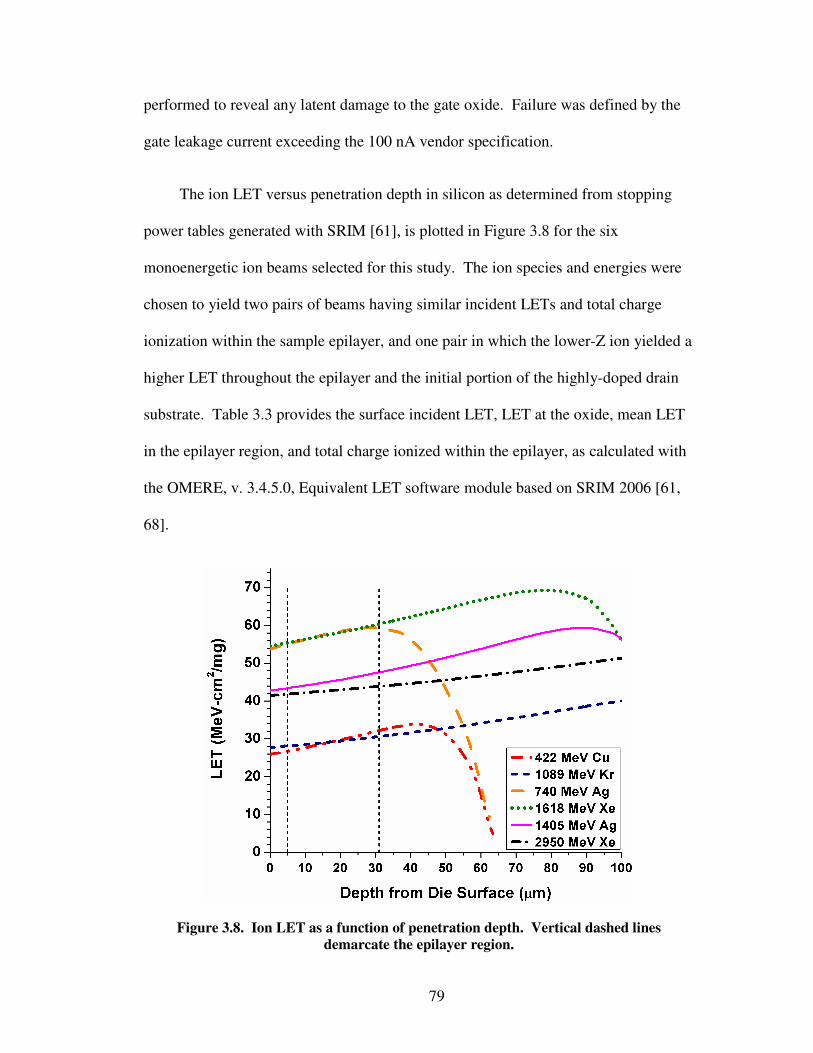
79
performed to reveal any latent damage to the gate oxide. Failure was defined by the
gate leakage current exceeding the 100 nA vendor specification.
The ion LET versus penetration depth in silicon as determined from stopping
power tables generated with SRIM [61], is plotted in Figure 3.8 for the six
monoenergetic ion beams selected for this study. The ion species and energies were
chosen to yield two pairs of beams having similar incident LETs and total charge
ionization within the sample epilayer, and one pair in which the lower-Z ion yielded a
higher LET throughout the epilayer and the initial portion of the highly-doped drain
substrate. Table 3.3 provides the surface incident LET, LET at the oxide, mean LET
in the epilayer region, and total charge ionized within the epilayer, as calculated with
the OMERE, v. 3.4.5.0, Equivalent LET software module based on SRIM 2006 [61,
68].
Figure 3.8. Ion LET as a function of penetration depth. Vertical dashed lines
demarcate the epilayer region.

80
Table 3.3. Ion Beam Properties for the 200V nVDMOS
Ion Energy Incident LET LET at Oxide
Mean LET within Epilayer
Total Charge Ionized in Epilayer
Z MeV MeV·cm2/mg MeV·cm
2/mg MeV·cm
2/mg pC
29 422 25.9 26.7 29.3 7.9 36 1089 27.7 28.1 29.3 7.9 47 740 53.8 55.5 57.8 15.5 54 1618 54.6 55.4 57.8 15.5 47 1405 42.7 43.4 45.4 12.2 54 2950 41.5 41.8 42.8 11.5
3.5.2 Results
The results of these experiments suggest that the ion species effect on the oxide
is a non-negligible contributor to gate rupture. In this study, the threshold drain-
source voltage for SEGR was determined for six different monoenergetic heavy-ion
beams. For four of these beams, the ions and energies were chosen to yield pairs that
would on average ionize the same total charge of either 7.9 pC or 15.5 pC within the
sensitive epilayer of the samples. In this way, the effect of ion LET was dampened to
reveal any ion species effects on SEGR susceptibility.
The first pairing consisted of irradiations by either 422 MeV copper (Z = 29) or
1089 MeV krypton (Z = 36). Three and four samples, respectively, were irradiated at
a fixed -10 Vgs, with the threshold Vds for SEGR found by incrementing the Vds by
5 V per beam run. Due to the small sample size and the interval nature of the data
from the experiments in this study, all data were analyzed as follows. We assume
that for each ion species and energy, the SEGR failure threshold Vds for the device

81
tested has a normal distribution from part-to-part variability. The method of
maximum likelihood [69, 70] was then employed to identify the mean (µ) and
standard deviation (σ) best fitting our experimental data. To further account for our
limited data set and hence the unknown extent of part-to-part variability, we use the
standard deviation at the boundary of the 90% confidence level instead of this best fit
value, using the Chi-square value for 2 degrees of freedom (µ and σ). We can use the
Chi-square distribution in this way because the distribution of each likelihood
estimator (µi and σi) tends toward a Gaussian with the best-fit value as the mean [64,
71].
Figure 3.9 plots these best-fit means for the copper and krypton data, with error
bars indicating one standard deviation from the mean at the boundary of the 90%
confidence level. As can be seen for the data taken at -10 Vgs, despite both ions on
average ionizing equal amounts of charge within the epilayer, SEGR occurs at a
lower Vds under irradiation with the heavier krypton ion. The difference in the mean
Vds for SEGR is significant at the 90% confidence level. As shown in Figure 3.9, we
further characterized the effect of copper versus krypton ions by irradiating two
additional samples with 422 MeV Cu, holding Vds at 130 V (a value within the
failure range for krypton at -10 Vgs), and incrementing Vgs by -1 to -2 volts. SEGR
occurred in both samples between -16 Vgs and -17 Vgs or -18 Vgs. These data
further support this apparent ion species effect.

82
Figure 3.9. SEGR response curve for Cu versus Kr irradiation. Both ions ionize on
average the same amount of charge within the epilayer, but yield SEGR responses at -10
Vgs that differ significantly at the 90% confidence level. At 130 Vds, samples irradiated
with Cu required more than -16 V on the gate before SEGR occurred.
Examination of the LET versus depth curves for the copper and krypton ion
beams (Figure 3.8) reveals a small difference in the distribution of ionized charge
within the epilayer, as well as a difference in total charge ionized within the heavily-
doped drain substrate region. To better understand the influence of ion species and
ion LET on SEGR susceptibility, we tested a second pairing of ions. Both 740 MeV
silver (Z = 47) and 1618 MeV xenon (Z = 54) ionize on average 15.5 pC in the device
epilayer with similar distributions (Figure 3.8). The same procedure as before was
followed, with 4 samples irradiated with Ag and 3 with Xe. The results are plotted in
Figure 3.10. The data suggest a difference between the two ion species but this shift
in the mean is not significant at the 90% confidence level. An additional sample was

83
irradiated with silver at a fixed Vds of 50 V, but the Vgs bias required for failure was
not significantly different than that for xenon under a 50 Vds bias.
Figure 3.10. SEGR response curve for silver versus xenon, at incident LETs of 54
MeV·cm2/mg. Error bars = one standard deviation bounding the 90% confidence level.
Lastly, the impact of ion species versus LET was evaluated by comparing the
bias necessary for SEGR under irradiation with 1405 MeV Ag to that under
irradiation with 2950 MeV Xe. Figure 3.8 shows that compared to the heavier xenon
ions, the silver ions will ionize more charge throughout the epilayer thickness, and
also through the first 70 µm or more of the highly-doped drain substrate region.
Irradiations were performed at -10 Vgs bias on 3 samples per beam condition
following the same procedures as before. Figure 3.11 shows that despite the silver
ions having a higher average LET throughout the epilayer and into a substantial

84
portion of the drain substrate region, a higher applied Vds was necessary for SEGR to
occur at -10 Vgs with silver as compared to with the heavier species, xenon. This
difference in failure threshold is significant at the 90% confidence level. This
difference was further substantiated by irradiating 2 additional samples with 1405
MeV silver at a drain bias of 50 Vds, near the mean of the threshold for SEGR from
xenon. Both of these additional silver samples experienced SEGR at -14 Vgs, having
last survived at either -12 V or -13 V.
Figure 3.11. SEGR response curves for 1405 MeV silver versus 2950 MeV xenon ions.
The lighter silver ions ionize more charge in the epilayer and initial 70 µµµµm of highly-
doped drain substrate, but require a statistically-significant higher applied Vds at -10
Vgs for SEGR to occur. Error bars indicate one standard deviation bounding the 90%
confidence level. With Vds set to the failure threshold found for xenon, silver-irradiated
samples failed at -14 Vgs.
85
3.5.3 Discussion and Implication for SEGR Hardness Assurance in Power
MOSFETs
Past studies have suggested that the ion atomic number may affect SEGR
susceptibility beyond simply the ion LET or total charge ionization [41, 58]. To our
knowledge, this study is the first to control for the charge ionization in the silicon
epilayer in order to examine the impact on SEGR of different ion species. Our results
suggest that the impact on the oxide due to the ion atomic number cannot be
neglected when considering SEGR risk avoidance on orbit.
As shown in Figures 3.9 – 3.11, for all three pairings of ions, the heavier ion
resulted in a lower mean Vds threshold for SEGR than did the lighter ion, despite the
lighter species ionizing the same or even more charge in the drain epilayer. This
difference was not significant for the silver versus xenon ions when their average
LET in the epilayer was 57.8 MeV·cm2/mg, but became significant at the 90%
confidence level when the average LETs were 45.4 MeV·cm2/mg and 42.8
MeV·cm2/mg, respectively. To examine the results of this study more closely, we
first identify the sources of deviation from the mean SEGR threshold biases.
The results presented in Figures 3.9 – 3.11 have large error bars that represent
the 90% worst-case upper bound on the standard deviation for the distribution of
failures. The small sample size, the Vds interval, part-to-part variability, and the
Poisson nature of the failures all contribute to this uncertainty in the best-fit mean. Of
these factors, the small sample size is likely the largest contributor, such that the
significance of the results in this study would likely increase with more data. The

86
impact of the other factors was lessened by a Vds increment of only 2.5% of the rated
BVdss, a single wafer diffusion lot for the samples, and a high fluence at each beam
run.
As indicated above, the lower mean threshold Vds for SEGR for 1618 MeV Xe
versus 750 MeV Ag (average LET in the epilayer = 57.8 MeV·cm2/mg) was not
significant at the 90% confidence level. In contrast, the 2950 MeV Xe irradiations
resulted in SEGR at a significantly lower Vds than did irradiations with the lighter
1405 MeV Ag ions, despite the silver ions depositing more energy in both the
epilayer and the initial 70 µm of highly-doped substrate (Figure 3.8). This result
suggests that the lack of significance at the 90% confidence level between 1618 MeV
Xe and 750 MeV Ag may be due to the small sample size and the Vds interval size.
Alternatively, we note that as the Vds bias is reduced, the depleted portion of the
epilayer is reduced; at -10 Vgs, there may be a minimum Vds for which SEGR can
occur for higher LET ions. Recall that at 0 Vds, we show that a -40 V gate bias is
required for SEGR to occur under xenon irradiation (see section 3.1). The lack of
significance between the xenon and silver ions with an average LET of 57.8
MeV·cm2/mg in the epilayer may be due to a bottoming-out of the minimum Vds bias
for SEGR to occur with xenon at -10 Vgs. The mean threshold Vds bias for the 57.8
MeV·cm2/mg (average LET) xenon differs only by 3.8 V from that of the 42.8
MeV·cm2/mg (average LET) xenon; in comparison, there is a 13.8 V difference
between the 57.8 MeV·cm2/mg and 45.4 MeV·cm2/mg silver. Finally, it is possible
that the relative effect of the ion species may lessen as the average LET in the
87
epilayer increases. Additional studies are needed to determine whether or when the
energy deposition in the silicon dominates the species effects on the oxide.
The variability in the Vds for SEGR was largest for the lightest ion tested. This
variability may be due to a decreasing cross-section for SEGR as ions become lighter
and/or deposit less energy: The lower-LET, lighter ion must strike closer to the
center of the drain region to cause SEGR, whereas heavier ions with higher LETs
may be able to rupture the gate regardless of the location of the strike within the drain
neck region. For a fluence of 3x10⁵ ions/cm2, 51,000 ions strike the die on average
during a single beam run. It is therefore unlikely that the total variability can be
explained by a changing SEGR cross section.
The 422 MeV Cu ions were obtained by passing the ion beam through a 2.8 mil
aluminum degrader. The use of a degrader results in a greater spread in the energy
range of the resulting ion beam due to energy straggling as ions pass through the
degrader material. We examine the spread of energies for this copper beam using the
Monte Carlo routine, TRIM, within the SRIM package [61]. Although the standard
deviation about the mean energy is small (2.7 MeV), the range of ion energies
extended from 220 MeV to 432 MeV. At energies below 360 MeV, copper can
ionize 8.5 pC or more (up to 8.75 pC), as opposed to the average 7.9 pC. The
probability of such a lower-energy copper ion striking the gate region of the sample is
small, but not zero: Of the ions striking anywhere on the die during a single beam
run, the Monte Carlo results suggest 0.02%, or 10 ions, would have energies below
360 MeV; of these 10 ions, about 30%, or 3 ions, would strike the gate region. If the
strike must be at the center of the drain neck region for SEGR to occur, then this

88
number is further reduced. A failure analysis on these samples to identify the
location of the gate rupture would possibly reveal whether the strike location was a
function of the bias needed for SEGR.
Finally, we note that charge ionized within the highly-doped drain substrate did
not have as much of an effect as the charge in the epilayer or the ion atomic number
on the SEGR failure threshold bias. In the case where silver ionized more charge in
both the epilayer and the first 70 µm of the substrate than xenon, the heavier xenon
ions ruptured the gate oxide at a significantly lower drain-source bias. Only charge in
the initial few µm of the heavily-doped substrate would be expected to contribute to
the transient electric field due to the deformation of the epilayer/substrate interface
drift field into the first few µm of the substrate at the location of the ion track due to
the large concentration of charge ionized; however, in the majority of the substrate
there is only a minimal electric field, such that charge would be collected primarily
by slower (and less efficient) diffusion processes. Additionally, this charge would
undergo comparatively higher recombination upon initial ionization. The important
ion beam characteristics for inducing SEGR therefore are the total energy it can
deposit in the epilayer and the ion atomic number. Our analysis so far suggests that
the higher ion atomic number gives rise to more damage in the oxide, thereby
lowering the electric field necessary for single-event gate rupture.
3.6 Summary
In chapter 2, we demonstrated the inadequacy of LET-based SEGR mitigation
methods due to ion range effects in the epilayer and ion species effects in the oxide.

89
In this chapter, we conducted experiments to explore further the effects of ion atomic
number on SEGR susceptibility. First, we validated the Titus-Wheatley expression
(4) for the critical field required for gate rupture as a function of only the oxide
thickness and the ion atomic number. Important to the device simulation
methodology developed in this dissertation, validation of this formula indicates that
the ion species simulated, Vgs applied, and gate-oxide thickness modeled are
sufficient for identifying when the simulated peak oxide electric field reaches a
magnitude necessary for rupture. We further investigated the Titus-Wheatley
expression through simulation, confirming that this formula captures the ion-oxide
interaction physics as separate from the effects of the charge ionized in the silicon
epilayer below.
We next focused on the complete SEGR mechanism, assessing the relative
importance of the heavy-ion interaction with the oxide, the charge ionized in the
epilayer, and the charge ionized in the drain substrate, on inducing SEGR. To our
knowledge, this study was the first to control for the charge ionization in the silicon
epilayer in order to examine the impact on SEGR of different ion atomic numbers.
Our results indicate that both charge ionized in the epilayer and the ion atomic
number are important parameters of SEGR failure, while the charge ionized in the
substrate is of secondary importance. We are now ready to assimilate the
contributions of our work so far into a new power MOSFET hardness assurance
approach for bounding the on-orbit risk of SEGR.

90
Chapter 4: A New Hardness Assurance Approach for Bounding the
On-Orbit Risk of SEGR
We have shown that the ion atomic number cannot be neglected in assessing on-
orbit risk for SEGR. When interpreting experimental or simulation data defining a
SEE response curve for a device to be flown in space, we therefore must move from
the one-dimensional space of flux versus ion LET, as was depicted in chapter 1 in
Figure 1.5, to a two-dimensional description of the heavy-ion environment in space:
flux versus ion atomic number and ion energy. In this chapter, we incorporate this
species effect into a new space mission SEGR hardness assurance approach that
depends on the specific heavy-ion environment flux as a function of both ion atomic
number and ion energy.
4.1 Applying the SEE Response Curve to the Two-Dimensional Heavy-Ion
Environment for a Space Mission
We move away from a one-dimensional description of the hazardous space
environment by recalling that LET is a function of both ion species and ion energy, as
shown in Figure 4.1 for a subset of the ion energies found in space. Note that we
have plotted energy in units of MeV/nucleon. To evaluate the risk of SEGR on orbit,
we must examine the flux of particles deemed hazardous to a given power MOSFET.
An example description of the space environment heavy-ion differential flux based on

91
ion species and energy is shown in Figure 4.2. In this figure, the ion flux was
calculated with the ISO15390 galactic cosmic ray model [72] for geostationary orbit
at solar minimum with 100 mils of aluminum shielding. At geostationary orbit, a
spacecraft has minimal protection from Earth’s magnetosphere, and at solar
minimum, the galactic cosmic ray flux is higher; 100 mils of Al represents minimal
shielding provided by the spacecraft walls and the device packaging.
Figure 4.1. Contour plot of ion LET as a function of atomic number and energy.
LETs are in units of MeV·cm2/mg.

92
Figure 4.2. Heavy-ion flux at geostationary orbit as a function of ion species and
energy.
We can use this heavy-ion environment matrix along with the SEE response
curve for a power MOSFET under consideration for a space mission to bound the on-
orbit risk for SEGR. We start by defining regions in this two-dimensional space for
which hardness to SEGR is assured, hardness is uncertain, and a region of known
SEGR susceptibility. For example, a common mission surface-incident LET
requirement for hardness assurance for power MOSFETs is 40 MeV·cm2/mg. In
chapter 2 we showed that accelerator facility test data for SEGR at this surface-
incident LET using silver ions as compared with bromine ions reduced the safe
operating area of a 200V power MOSFET due to ion range and, based upon the
results in section 3.4, silver’s higher atomic number. We then simulated the SEE
response curve for the even heavier gold ion, as shown in Figure 2.7. Figures 4.3A –
4.3C identify the safe portion of the differential ion flux when a device is operated

93
within the derated SEE response curve defined by either Br, Ag, or Au ions with an
incident LET of 40 MeV·cm2/mg. This area encompasses ion species lighter than the
test species, with energies yielding LETs below 40 MeV·cm2/mg (refer to Figure
4.1). Also identified is a region of uncertainty that includes both heavier species with
higher energies (lower LETs) and lighter species with lower energies (higher LETs),
than that used to define the SEE response curve; these will add to the SEGR
hardness-assured portion of the spectra to an unknown extent. Finally, a region of
known SEGR susceptibility is defined for ions with LETs greater than 40
MeV·cm2/mg having higher atomic numbers than that used to define the SEE
response curve. Without further data, the upper bound of hazardous flux would be
the integral of the flux in the latter two regions: the area of uncertainty and the area
of known risk. The lower bound would then be just the integral of the flux in the
region of known risk.
Figure 4.3A-C (next page). A portion of the heavy-ion spectrum showing the hardness
assurance provided by derating the SEE response curve for Br (A), Ag (B), or Au (C).
The solid navy-blue region indicates the region of heavy-ion flux that will not induce
SEGR on-orbit. Red areas are regions of known risk; graded areas outlined in light
blue are regions of unknown risk.

94
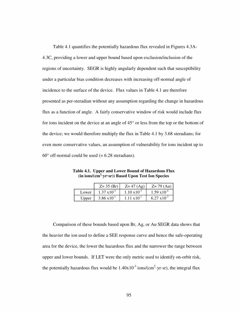
95
Table 4.1 quantifies the potentially hazardous flux revealed in Figures 4.3A-
4.3C, providing a lower and upper bound based upon exclusion/inclusion of the
regions of uncertainty. SEGR is highly angularly dependent such that susceptibility
under a particular bias condition decreases with increasing off-normal angle of
incidence to the surface of the device. Flux values in Table 4.1 are therefore
presented as per-steradian without any assumption regarding the change in hazardous
flux as a function of angle. A fairly conservative window of risk would include flux
for ions incident on the device at an angle of 45° or less from the top or the bottom of
the device; we would therefore multiply the flux in Table 4.1 by 3.68 steradians; for
even more conservative values, an assumption of vulnerability for ions incident up to
60° off-normal could be used (= 6.28 steradians).
Table 4.1. Upper and Lower Bound of Hazardous Flux
(in ions/(cm2·yr·sr)) Based Upon Test Ion Species
Z= 35 (Br) Z= 47 (Ag) Z= 79 (Au)
Lower 1.37 x10⁻³ 1.10 x10⁻³ 1.59 x10⁻⁴ Upper 3.86 x10⁻¹ 1.11 x10⁻¹ 6.27 x10⁻³
Comparison of these bounds based upon Br, Ag, or Au SEGR data shows that
the heavier the ion used to define a SEE response curve and hence the safe-operating
area for the device, the lower the hazardous flux and the narrower the range between
upper and lower bounds. If LET were the only metric used to identify on-orbit risk,
the potentially hazardous flux would be 1.40x10⁻³ ions/(cm2·yr·sr), the integral flux

96
for all species with LET ≥ 40 MeV·cm2/mg. Table 4.1 suggests that this value would
under-predict the true geosynchronous-orbit hazard.
Following this example, the following algorithm defines the upper bound of
potentially hazardous flux (ФUB) when biasing a device at the limit of the safe
operating area defined by a given ion species, Zi, having a given mission LET
requirement, LETi:
.dLETdZ)LET,Z(dLETdZ)LET,Z( )LET ,(Z 921
119
iLET92
1iZiLET
0iiUB ∫ ∫ ∫ ∫+=Φ∆+ +
φφ (9)
The first term in (9) captures all flux of ions with energies yielding LETs above the
mission LET requirement (this integral encompasses the known hazardous flux and
the portion of unknown hazardous flux in which the species is lighter than the test
ion, but has a higher LET). The second term includes the unknown hazardous flux in
which the ion species is heavier than the test ion, but the LET is less than the mission
LET requirement (and hence less than the test LET). Note that for now, we do not
make any assumptions about the lower limit of the hazardous LET for these heavier
ion species.
In Figure 4.4, we re-plot the differential flux of ions at geostationary orbit
shown in Figure 4.2 as the reverse-integral flux as a function of ion species and LET.
In this plot (Figure 4.4), the flux has been reverse-integrated over both ion species
and LET, such that for any given species and LET, the flux shown is the total flux for

97
that atomic number and LET plus that of all higher atomic numbers and LETs1. From
this reverse-integral flux plot, it is then easy to extract the upper bounds of hazardous
flux for any combination of test ion species and LET; we show the resulting initial
plot of upper bounds in Figure 4.5A. Figure 4.5A includes non-physical
combinations of species and LETs, that is, the upper bound of hazardous flux for ion
species at LETs higher than are physically possible. We eliminate these
combinations, and our final solution of (9) is the plot in Figure 4.5B. In Figure 4.5B,
we have labeled the points corresponding to the ion species (Br, Ag, and Au) used in
our example above for a mission LET requirement of 40 MeV·cm2/mg (see Figure
4.3 and Table 4.1).
Figure 4.4. Reverse-integral flux over both ion atomic number and LET, at
geostationary orbit during solar minimum behind 100 mils Al shielding.
1 To calculate the reverse-integral flux over both Z and LET, we have worked with the output of the ISO15390 galactic cosmic ray model and the SRIM-based LET spectrum calculation within the OMERE v.3.4.6.1 software package [64].

98
A.
B.
Figure 4.5. Upper bound of hazardous flux (per steradian of vulnerability) at
geostationary orbit during solar minimum behind 100 mils Al shielding, as a function of
test ion species and incident LET. Panel A shows the solution to (9); panel B shows the
final result after removing non-physical combinations of ion species and LETs.

99
Further refinement of (9) and hence a reduction of the upper bound of hazardous
flux would require more detailed studies to identify the relative importance of ion
species versus energy deposition, as well as the angular response, for the specific
device under consideration. We have already incorporated our knowledge from
chapter 3 suggesting that for comparable energy deposition in the epilayer, the
heavier ion will induce SEGR at a lower threshold bias; this incorporation led to
regions of unknown risk in the flux vs. Z vs. energy (or LET) matrix describing the
space environment. We now adapt the simulation methods we developed in chapter 2
to reduce the amount of flux that composes this unknown risk by examining for what
incident LET a heavier ion will have the same SEGR threshold as a lighter 40
MeV·cm2/mg TAMU test ion. Such a determination cannot be made at accelerator
facilities commonly used for single-event effect evaluation because a heavier ion such
as gold would require acceleration to 100 – 200 MeV/u!
4.2 Applying SEGR Simulation Methods to Narrow the Bounds of the Hazardous
Flux
We refine the upper bound of hazardous flux using the methods developed in
chapter 2. Recall that in chapter 2, we extracted the geometry and doping profile of a
power MOSFET from a small set of test data, and successfully developed a predictive
SEGR response model of the device. We demonstrated how such models could be
used to obtain additional SEGR data without performing further expensive accelerator
beam tests. For the 500 V p-type power MOSFET examined in chapter 2, we have
100
both simulated and experimental data defining a SEE response curve for 21 MeV/n
xenon with an incident LET near 40 MeV·cm2/mg (Figure 2.8). We now wish to
identify the maximum energy a heavier ion can deposit before causing SEGR when
the device is biased on this SEE response curve for xenon; i.e., the energy at which
that heavier ion would yield the same SEE response as that of xenon, for a particular
Vgs. Toward this end, we simulate gold ion strikes of various energies while biasing
the model at 0 Vgs and -100 Vds. This bias was the highest magnitude before SEGR
occurred under xenon irradiation. We find that a simulated gold ion strike having an
incident LET of 25 MeV·cm2/mg results in SEGR, but that simulations for an
incident LET of 20 MeV·cm2/mg show a transient maximum oxide electric field
below that required for SEGR.
We repeat this simulation experiment in the 200 V nVDMOS model, setting the
bias at 0 Vgs and 100 Vds, the simulated threshold for SEGR under 40 MeV·cm2/mg
silver irradiation (Figure 2.6). Again, we find that at 25 MeV·cm2/mg, the gold ion
induces a transient maximum oxide electric field just greater than that required for
SEGR, but that at 20 MeV·cm2/mg, no SEGR occurs. In both devices, we therefore
find that for LETs at or below half our test ion LET, gold ions (Z=79) will not cause
SEGR when the device is biased at the maximum safe Vds determined by our test ion.
We can thus incorporate our SEGR simulation methodology with our method
for defining the heavy-ion hazardous environment for a power MOSFET under
consideration for a space mission. As an initial conservative reduction of the upper
bound of hazardous flux, we assume that for any given test species and LET, only
those heavier species having LETs greater than half the test LET may pose a hazard.

101
We therefore raise the lower limit of integration over LET in the second term of (9)
from 0 to ½ LETi. The result of this refinement of the upper bound of hazardous flux
is shown in Figure 4.6.
Figure 4.6. Refined upper bound of hazardous flux (per steradian of
vulnerability) at geostationary orbit during solar minimum behind 100 mils Al
shielding, as a function of test ion species and incident LET.
As an example, for both the 500 V commercial pVDMOS and the radiation-
hardened 200 V nVDMOS, the risk of SEGR when biased at 0 Vgs and a Vds within
the safe-operating area for a mission LET requirement of 40 MeV·cm2/mg would
now be bounded according to the hazardous flux values given in Table 4.2.
Table 4.2. Upper and Lower Bound of Hazardous Flux (in ions/(cm2·yr·sr)) Based
Upon Test Ion Species and Simulations to Refine the Upper Bounds.
Z= 35 (Br) Z= 47 (Ag) Z= 79 (Au)
Lower 1.37 x10⁻³ 1.10 x10⁻³ 1.59 x10⁻⁴ Upper 7.99 x10⁻³ 6.23 x10⁻³ 2.26 x10⁻³
102
4.3 Proposed Methods for Further Refinement of the Upper Bound of Hazardous
Flux
We can extrapolate a method for further refinement of the upper bound to the
on-orbit hazardous flux for SEGR in which the threshold ionizing energy deposition
(LET) is identified for each ion contributing flux in the regions of hazard uncertainty.
In our example, we found the maximum safe energy deposition for gold ions (Z=79)
to be that corresponding to an incident LET of 20 MeV·cm2/mg, when our devices
are biased at 0 Vgs and the threshold Vds for SEGR from either xenon (Z=54) or
silver (Z=47). We know that as the atomic number of the ion species nears that of the
test ion, the maximum safe incident LET will approach that of the test ion; our
refinement in Figure 4.6 is therefore likely overly conservative. As we have stated
previously, additional studies are needed to better understand the relative
contributions of ion species and ion LET on the threshold bias for SEGR. As part of
our immediate future work, we can use simulations to give us a preliminary
understanding.
To this end, we need not find the incident LET for every ion species that would
yield the given threshold Vds for SEGR. Instead, we can make the assumption that to
first order, the distribution of the ionized charge along the ion track does not
influence the resulting transient oxide electric field. Keeping the device model at the
threshold failure bias of interest, we can simulate ion strikes using a constant LET
value throughout the epilayer thickness and find the resulting maximum oxide field
for this constant LET. Repeating this method for a set of LET values, we can build a
matrix of peak oxide fields and corresponding LETs for a given device. These values

103
are independent of the ion species since the simulations do not incorporate the oxide
response to the ion strike. Using the Titus-Wheatley formula (4), we can identify the
critical field necessary for rupture for each ion species contributing flux in the region
of hazard uncertainty, and assign the corresponding constant LET required for that
species to induce SEGR under the bias conditions of interest. Translation of that
constant LET into a minimum surface-incident LET yielding that energy deposition
results in a new lower bound of integral flux (over LET) for that species.
In this way, the region of hazard uncertainty, for example as shown in Figure
4.3, is slowly divided into areas where hardness is assured and areas of known risk.
The mission-specific hazardous flux for the given device under the maximum safe
Vds bias for a given Vgs, therefore, will be defined within a margin of error
stemming from the fidelity of the simulations, experimental SEE response curve
determination, solid angle of SEGR vulnerability, and radiation environment models.
4.4 Step-by-Step: The New SEGR Hardness Assurance Approach Summarized
The work detailed in this dissertation indicates that it would be advantageous to
introduce a new SEGR hardness assurance approach that considers the importance of
the ion atomic number and therefore the oxide response as separate from the effects
of the charge ionized within the silicon epilayer. Using the example of a
geostationary orbit and a mission LET requirement of 40 MeV·cm2/mg, we have
outlined such a hardness assurance approach. We now summarize this approach for
any flight mission:

104
1) Find or take SEGR response curve data for a given mission LET
requirement. Older vendor data from low-energy test ions may be used since our
method for bounding the SEGR failure rate includes longer range ions with the test
LET as hazardous flux.
2) Define the heavy-ion radiation environment for the mission orbit and solar
activity level. A design margin may be placed on the results to allow for limitations
of the environment model fidelity.
3) Convert the radiation environment into reverse-integral flux integrated over
both ion species and ion LET.
4) Solve (9) for the test ion species and test LET used to define the SEE
response curve for the power MOSFET under consideration. This solution yields the
upper bound of hazardous flux, which can be converted into an upper bound for the
SEGR failure rate. This conversion is as follows:
f⋅−⋅⋅⋅Φ= ))cos(1(4ANRate UBUB θπ (10)
where N is the number of devices to be flown, A is the SEGR cross-section of the
device (equal to the gate area of the die; if unknown, the total die area can be used as
a conservative number), θ is the maximum off-normal angle of incidence for which
the device is vulnerable to SEGR, and f is the fraction of time the device will spend in
the off state (off-state duty cycle).
5) Ask the following two questions:

105
a) Is the upper bound of the failure rate acceptable for the device
application? If yes, move to b). If no, the flight project may consider simulating an
ion species and LET combination that will yield an acceptable upper bound. Making
a plot like that shown in Figure 4.6 is a useful way to determine the combination
required to be simulated.
b) Will the device’s maximum off-state static AND transient biases
remain within the safe-operating area defined by applying a 0.75 derating factor to the
SEE response curve for the test or simulated ion species and energy? If yes, the
device can be qualified for the mission. If no, our simulation methodology for
determining the device-specific appropriate derating factor can be used to maximize
the usable portion of the device voltage-blocking capability. Alternatively or in
addition, the plot of upper bounds of hazardous flux as a function of ion species and
LET can be further refined by performing the simulations proposed for rapidly
identifying the minimum LET for each species resulting in SEGR when the device is
biased at the maximum off-state voltage divided by the derating factor. Such
refinement may yield an acceptable upper bound in the failure rate for the application
bias condition. If so, the device can be qualified.
4.5 Summary
Based upon our results from chapters 2 and 3 concerning the importance of ion
species and energy on SEGR susceptibility as opposed to simply ion LET, we
developed a new hardness assurance approach for bounding the on-orbit risk of
SEGR. We demonstrated the refinement of the upper bound through the use of our
106
simulation methods developed in chapter 2, and proposed an approach for identifying
the hazardous flux for a device operating at the maximum Vds within a derated SEE
response curve, within a margin of error stemming from the underlying steps
involved. This hardness assurance approach for establishing a bound on the risk of
SEGR for a given device, together with the methodology we developed in chapter 2
for refining the derating factor to be applied to the given device, provides radiation
physicists with tools for quantifying the basis for their decisions in permitting or
barring the insertion of specific power MOSFET into a space flight mission.

107
Chapter 5: Improvement of Our Understanding of How
Accumulated Dose Affects SEGR Susceptibility
5.1 Motivation
SEGR risk assessment and mitigation are based upon pristine device
performance under heavy-ion irradiation. Total dose hardness is treated as a separate
issue. The potential for accumulated dose to impact single-event outcomes is
therefore normally not considered. The research on the potential coupling of dose
and SEGR susceptibility is sparse; therefore, the risk of increasing SEGR
susceptibility with mission lifetime in non-hardened power MOSFETs or on high
total-dose missions is unknown at this time.
A simplistic response to this radiation hardness assurance question is to require
the use of total-dose hardened power MOSFETs. The choice of commercial versus
radiation-hardened power MOSFETs, however, is a trade space. Hardened devices
substantially reduce total ionizing dose concerns. Recent generations of devices
fabricated by International Rectifier (IR) even demonstrate increased SEGR hardness
[73]. Despite these hardening efforts, dose effects on the threshold bias for SEGR
were found on a recent-generation hardened 1000V IR device after exposure to a
proton fluence not unrealistic for a mission flying through the radiation belts [54].
Early-generation radiation-hardened devices (hardened for total dose, not for SEGR)
are still commonly used for space applications due to adherence to heritage designs or
108
due to the trade space between SEGR hardening and on-state resistance. From a
design engineer’s perspective, the higher on-state resistance of a hardened device eats
into a greater portion of a circuit board or instrument box’s total power allocation.
This factor combined with the fewer choices of breakdown (BVdss) ratings and
generally lower current ratings for a given BVdss make commercial device offerings
appealing to a designer. Finally, from a procurement standpoint, hardened devices
are much more expensive and lead times to obtain devices can extend from months to
over a year.
Commercial devices provide better electrical performance. High currents and
low on-state resistances are easily found. These devices are much cheaper to procure
and are usually readily available. From a radiation hardness assurance perspective,
however, they present challenges. Due to their thick oxides, the devices are very
sensitive to total ionizing dose effects as compared with traditional MOSFETs, and
poorer quality oxides can result in increased susceptibility to SEGR. Higher-quality
non-radiation hardened power MOSFETs can be obtained from a Qualified
Manufacturer List (QML) supplier. QML parts must meet strict government
standards to provide greater reliability assurance for the extreme environments of
many military applications. The JANS (Joint Army-Navy/Space level) class of
devices has the highest level of screening. The JANS qualification level provides no
assurances for radiation reliability, however.
Understanding the effects of dose on SEGR susceptibility will help guide
appropriate device selection and radiation test methodology. In this way, radiation
hardness assurance of power MOSFETs will cover the “cradle-to-grave” cycle of a
109
space flight project. In this chapter, past investigations of total ionizing dose effects
on SEGR are summarized. We then present what is, to our knowledge, the first study
of SEGR susceptibility in gamma-irradiated commercial power MOSFETs. We
follow this study with surprising results on the effects of dose from gamma rays
versus dose from heavy ions and provide a plausible explanation for these findings.
5.2 Prior Understanding of Effects of Total Dose on SEGR Likelihood
5.2.1 Gamma Irradiation
Studies are mixed as to whether accumulated dose from gamma rays effects
SEGR susceptibility. Titus, et al. [35] compared SEGR bias thresholds of pristine
total-dose radiation-hardened 60V n-channel MOSFETs to those having received 400
krad (Si) accumulated dose. The gate oxide thickness for these devices was 50nm;
dose was delivered under a +10V gate bias (a bias usually resulting in greatest dose
effects on gate threshold voltage due to a higher hole yield in the oxide and due to the
positive bias driving the holes closer to the Si/SiO2 interface). A 9-V shift in the gate
threshold voltage was measured. Under non-zero drain-source biases, SEGR
occurred in the gamma-ray dosed devices at a lower magnitude of bias on the gate as
compared with the pristine devices. This difference was smaller for ions with an LET
of 60 MeV·cm2/mg than for an LET of 37 MeV·cm2/mg. The authors note that the
difference in gate bias threshold for SEGR disappeared for both LETs when the
devices were irradiated at a 0-V drain-source bias, suggesting that the gamma-ray
dose affects the epilayer response to the ion strike, but not the oxide response leading
to SEGR [35].
110
The amount of dose from gamma rays that these devices received is very high in
light of the majority of NASA missions experiencing less than 100 krad (Si) total
dose over their lifetime. This high dose was needed for this study to induce dose
effects in the radiation-hardened test samples. To better understand what the possible
effect on the epilayer response may be, we must understand the effects of gamma
irradiation. Gamma rays primarily lose energy in silicon or silicon dioxide through
creation of Compton electrons. In the oxide, the principle radiation effect results
from trapping of ionized holes within the oxide and the formation of amphoteric traps
at the oxide/silicon interface. In the silicon, damage results from the Compton
electrons displacing atoms from the lattice. These displacements form traps in the
energy band gap and can result in carrier removal; the defects can also degrade carrier
mobility due to increased scattering [74]. Unlike the damage created from higher-
energy particles, the displacement damage cascade from gamma irradiation will be
small due to the low energy of the primary knock-on atom (the atom initially
displaced by the Compton electron) [13]. We may initially hypothesize that Titus’
findings that suggest the gamma dose impacts the epilayer mechanisms involved in
SEGR, rather than the oxide mechanisms, are a function of the very high level of dose
given to the VDMOS prior to SEGR testing. Given enough dose, enough
displacement damage in the epilayer could have occurred to impact the epilayer
response to the heavy-ion strike.
A study of Rdson as a function of dose from either gamma or neutron irradiation
[75] reveals that this may not be the case, however. Measurements of Rdson can be
used to monitor the extent of displacement damage in the drain region [76]. In this

111
study, the primary effect of gamma irradiation on Rdson was through the shift in gate
threshold voltage due to charge trapping in the oxide, even at 1 Mrad (Si) dose levels.
Neutrons, which are not directly ionizing, had their primary effect through increasing
the resistivity of the drain epi-region as a result of displacement damage. It therefore
does not seem likely that the gamma dose effects on SEGR found for non-zero drain-
source biases in a radiation-hardened power MOSFET are due to displacement
damage in the drain epitaxial region.
A study of gamma irradiation of p-type MOS capacitors and the subsequent
effect on SEGR susceptibility was performed by Lum, et al., [45]. The capacitors
were specially processed using high-temperature anneals in order to increase the
number of defects in the 60 nm thick oxides. These capacitors received 200 krad (Si)
under a +40V gate bias, producing a C-V shift of -30 V. The critical voltage for
SEGR at an LET of 82 MeV·cm2/mg was not affected by this prior exposure to
gamma-ray irradiation when biased in accumulation or in depletion mode; dosed
capacitors were also tested for SEGR at an LET of 37 MeV·cm2/mg, though it is
unclear whether comparisons were made to identical capacitors irradiated at this LET
but having no prior dose accumulation. Lum, et al., conclude that the trapped charge
in the oxide due to accumulated dose prior to heavy-ion exposure does not affect the
SEGR response.
Lum, et al., [45] refer to work by Candelori, et al. [77] that demonstrates
Fowler-Nordheim tunneling of electrons from the silicon substrate of thin-oxide
pMOS capacitors reduces the effects of hole trapping in the oxide from heavy-ion
accumulated dose, suggesting that this same mechanism may be at play in

112
diminishing the role of trapped charge from gamma irradiation on the threshold bias
needed for SEGR. Fowler-Nordheim tunneling current is a function of the oxide
field, not the oxide thickness [78]. This mechanism may therefore be responsible for
Titus’ finding in the radiation-hardened nVDMOS that the gamma pre-irradiation did
not affect SEGR susceptibility at 0 V drain-source bias (but did for non-zero Vds
biases): At a 0 V drain-source bias, very high applied gate biases are needed to
induce SEGR (see chapter 3, section 3.1).
5.2.2 Proton Irradiation
The only other study in the published literature (to our knowledge) to examine
past dose effects on SEGR susceptibility considers dose from protons [54]. In this
study, accumulation of dose from proton irradiation was shown to reduce the bias
threshold necessary for SEGR during subsequent heavy-ion irradiation in both
commercial and total-dose radiation-hardened power nVDMOS. Commercial devices
were more susceptible to SEGR as a function of proton dose than were total-dose
radiation-hardened devices; both versions exhibited stronger dose effects on SEGR
susceptibility when irradiated with xenon at an incident LET of 40 MeV·cm2/mg than
with krypton at 20 MeV·cm2/mg. Tested devices included 100V, 500V, and 1000V
ratings; the 1000V commercial and radiation-hardened devices showed the greatest
decrease in threshold bias for SEGR as a function of prior proton dose. The authors
note that of the three parameters affected during proton irradiation (transconductance,
off-state leakage current, and gate threshold voltage), only the gate threshold voltage
trended with the bias required for SEGR, such that for a given device, the SEGR
threshold bias decreased with increasing shift in the gate threshold voltage.

113
Examination of data presented in [54] suggests that this relationship is fairly weak,
with the only significant linear correlation occurring for the commercial 1000V
device irradiated with 40 MeV·cm2/mg xenon – the combination showing the
strongest dose effect on SEGR susceptibility. Unlike the gamma-irradiation studies
above in which the devices were dosed under a positive or negative gate bias, the
device nodes in [54] were left floating during exposure to protons. The bias during
total ionizing dose exposure affects the yield of trapped charge in the oxide as well as
the subsequent hole migration [19, 21]. It is therefore difficult to draw conclusions
regarding the mechanisms by which proton irradiation may influence the bias
necessary to trigger SEGR.
5.3 SEGR Experiments on Dosed Power MOSFETs
From our review of past work on total dose effects on SEGR susceptibility, it is
clear that additional research is needed to determine whether this issue warrants
consideration in SEGR hardness assurance approaches, and to aid our understanding
of the possible mechanisms of this interaction of dose and SEGR. We therefore
conduct experiments on a commercial power MOSFET, exposing samples first to
various levels of gamma irradiation and then testing them for SEGR. We use a
commercial device in order to better reflect applications in which dose at typical
mission levels would be a concern. We choose gamma irradiation to focus on the
potential effects of charge trapping in the gate oxide as opposed to displacement
damage in the epilayer, given our above critique of the previous work in this area.
5.3.1 Experimental Methods: Gamma Irradiation
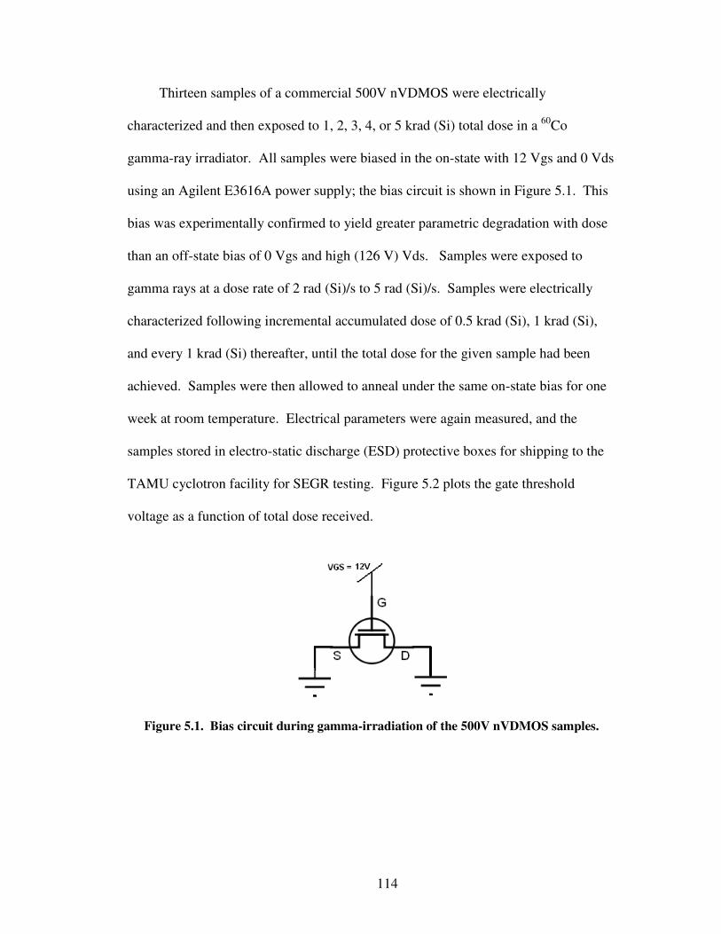
114
Thirteen samples of a commercial 500V nVDMOS were electrically
characterized and then exposed to 1, 2, 3, 4, or 5 krad (Si) total dose in a 60Co
gamma-ray irradiator. All samples were biased in the on-state with 12 Vgs and 0 Vds
using an Agilent E3616A power supply; the bias circuit is shown in Figure 5.1. This
bias was experimentally confirmed to yield greater parametric degradation with dose
than an off-state bias of 0 Vgs and high (126 V) Vds. Samples were exposed to
gamma rays at a dose rate of 2 rad (Si)/s to 5 rad (Si)/s. Samples were electrically
characterized following incremental accumulated dose of 0.5 krad (Si), 1 krad (Si),
and every 1 krad (Si) thereafter, until the total dose for the given sample had been
achieved. Samples were then allowed to anneal under the same on-state bias for one
week at room temperature. Electrical parameters were again measured, and the
samples stored in electro-static discharge (ESD) protective boxes for shipping to the
TAMU cyclotron facility for SEGR testing. Figure 5.2 plots the gate threshold
voltage as a function of total dose received.
Figure 5.1. Bias circuit during gamma-irradiation of the 500V nVDMOS samples.

115
Figure 5.2. Effect of accumulated dose from gamma irradiation on gate threshold
voltage. Green line demarcates the minimum vendor specification for the gate
threshold voltage. Error bars = 1 standard deviation.
5.3.2 Results: Gamma-Irradiation
The 500V commercial nVDMOS proved very sensitive to gamma irradiation.
As shown in Figure 5.2, the gate threshold voltage of the dosed devices shifted below
the vendor’s minimum specification (indicated by the green line) between 0.5 krad
(Si) and 1 krad (Si) accumulated dose. After 5 krad (Si), the average gate Vth was
just 0.33 V. The decrease in threshold voltage with dose is approximately linear as
expected by the relationship between the shift in threshold voltage (∆Vth) as a
function of dose given in [79], where it is assumed that all of the holes are trapped
near the interface:

116
ox
thth C
DAF(E)fqN- V ox
t=∆ . (6)
In this equation, q is the electronic charge of a hole, Nh is the initial number of
electron-hole pairs (ehp) ionized in the oxide per cm3 per krad (SiO2), tox is the oxide
thickness (in cm), A is the area under the gate, F(E) is the ehp yield fraction, ft is the
faction of holes trapped at the Si/SiO2 interface, and D is the radiation dose in krad
(SiO2).
We can use equation (6) to determine the approximate fraction of ehp that
survive initial recombination. From [80] which gives a plot of the ehp yield fraction
as a function of oxide electric field under gamma irradiation, we determine that the
yield fraction for our device is between 0.52 and 0.62. Here, we have assumed that
the gate oxide thickness is between 150 nm and 200 nm (per the vendor), when
calculating the oxide electric field at 12 Vgs bias during irradiation. Per [79] where it
is assumed that 18 eV are necessary to form an ehp in silicon dioxide, Nh becomes 7.6
x1015 ehp/cm3/krad (SiO2). We convert this value to per krad (Si) to match our data
by multiplying Nh by the ratio of the density of silicon over the density of SiO2,
resulting in Nh = 7.8 x10¹⁵ ehp/cm3/krad (Si). Taking Cox as (3.45 x10⁻¹³
F/cm)·(A/tox), we reduce (6) to:
D f F(E) t103.62- V t
2
ox
9
th ×=∆ . (7)
From our plot in Figure 5.2, we find the slope of ∆Vth/D for our device is -0.71
V/krad (Si). We find that over the range of oxide thicknesses of 150 nm to 200 nm,
the trapped hole fraction becomes less than one at thicknesses greater than 190 nm,

117
suggesting that our device may have an oxide thickness of at least 190 nm. Taking tox
as 200 x10-7 cm, the resulting fraction of trapped holes is 0.94. We would expect a
high trapping factor given the thickness of the oxide and the increasing likelihood of
holes to become more deeply trapped as they travel through the oxide [18].
The one-week room-temperature anneal under bias following 5 krad (Si) dose
resulted in only an 11% recovery in the shift in the gate threshold voltage. For oxides
on the order of 100 nm thick or more, deep trapping of holes occurs roughly within
20 nm of the Si/SiO2 interface where defects from excess Si are concentrated during
oxide growth [13, 81]. Electron tunneling is one of the mechanisms by which trapped
holes can be neutralized over time. This tunneling extends to only the initial 5 nm to
10 nm [13, 81, 82]; we may assume therefore that the majority of trapped holes in the
oxide lie 5 nm to 20 nm above the Si/SiO2 interface. Upon application of an off-state
bias to the power MOSFET during subsequent heavy-ion testing, this relatively
narrow band of holes may add to the heavy-ion induced transient increase in the oxide
field resulting from the separation of ionized charge in the epilayer drift field.
We conduct one final analysis of the total ionizing dose results before reporting
on the effect this dose has on the SEGR susceptibility of this device, in order to more
fully understand the nature of the trapped charge in the oxide due to the gamma
irradiation. In Figure 5.3, we plot the subthreshold drain current as a function of Vgs
at each dose point for one of the samples. The curves were measured with a
HP4156B parametric analyzer at a fixed Vds of 5 V; due to the power limitations of
the HP4156B, all curves in Figure 5.3 flat-line at the 100 mA current limit. The
leftward shift of the IV curves with increasing dose is due to the buildup of trapped

118
holes in the oxide. What we learn from Figure 5.3 is that despite the low level of total
dose exposure and the thick gate oxide, some interface trap buildup has occurred.
These interface traps reduce the switching speed of the device [83], as evidenced in
Figure 5.3 by the decrease in subthreshold slope following 5 krad (Si) dose as
compared to the pre-irradiation slope (green dotted line). Interface traps are
amphoteric, changing their sign as a function of their location relative to the Fermi
level. In n-type MOSFETs, these traps become negative as the energy bands bend
down as the transistor bias passes from flatband towards strong inversion [84] (see
section 1.3.1 for a description of the interface trap). This negative trapped charge
opposes the positive gate bias, stretching out the subthreshold IV curve.
Figure 5.3. Subthreshold IV curves as a function of total accumulated dose. The
pristine device IV curve is shown in blue. The slope of the IV curve following 5 krad
(Si) accumulated dose is compared to that of the pristine device (shown as the green
dotted line). The change in slope is a result of interface trap buildup.

119
Following the method of McWhorter and Winokur [84], we can isolate the
effects of the interface traps from the bulk traps on the total threshold voltage shift.
The shift due to interface traps is found by comparing the difference between the
threshold voltage and the extrapolated flatband voltage, for two IV curves; the shift
due to bulk oxide trapped charge is simply the difference between extrapolated
flatband voltages. The result is shown in Figure 5.4. As we would expect from the
oxide thickness and Figure 5.3, the threshold voltage shift is dominated by the oxide
bulk traps.
Figure 5.4. Total gate threshold voltage shift as a function of dose (Vth, red line) is a
sum of the shift due to oxide trapped charge (Vot, blue line) and interface trapped
charge (Vit, green line).

120
In summary, we have shown that the gamma irradiation of this device has
resulted in a large negative shift in the gate threshold voltage as a function of total
dose. At only 1 krad (Si) accumulated dose, the gate Vth was out of vendor
specification, having dropped below 3.0 V. By 5 krad (Si), the average gate Vth had
dropped to 0.33 V, a 3.38 V decrease from the average pre-dose value. Use of
equation (6) confirms that a large fraction (0.94) of the hole yield becomes trapped.
Based upon only an 11% recovery of the gate Vth upon a one-week anneal and our
understanding of deep trap formation and annealing processes, we expect a large
concentration of the oxide trapped holes to be located between 5 nm and 20 nm above
the Si/SiO2 interface. Finally, using the methods of McWhorter and Winokur [84],
we show that as expected in thick oxides, the shift in threshold voltage is dominated
by the effect of bulk oxide hole trapping with only a minimal opposing contribution
due to interface trap formation. We now examine the impact of this total
accumulated dose due to gamma irradiation on SEGR susceptibility.
5.3.3 Heavy-Ion Experimental Test Methods
Heavy-ion SEGR tests were performed on the 13 dosed samples, as well as 4
pristine (undosed) samples, at TAMU. Test methods were similar to those described
in section 2.2. Briefly, a Keithley 2400 SMU provided the gate voltage while
measuring the gate current and an Agilent 6035A power supply provided the
appropriate Vdd. At the drain and source, voltage data were collected using
HP34401A digital multimeters placed across a 1 Ω, 50W resistor at the source node
and at the drain node; these data as well as the gate current read from the Keithley
2400 were recorded via GPIB at approximately 100 ms intervals. The test method

121
and circuit are as shown in Figure 2.2 A-B. Figure 5.5 shows samples ready to be
aligned in the beam at TAMU.
All tests were performed at 0 Vgs to mirror a typical flight application bias. Vds
was incremented by 10 V at each beam run until sample failure occurred. Samples
were irradiated at normal incidence in air with 1170 MeV (surface-incident energy)
silver ions at a flux of 5x10³ ions/cm2/s to a maximum fluence of 1x10⁵ ions/cm2 per
beam run. At the end of each beam run, a post-irradiation gate stress test was
performed and the gate threshold voltage measured.
Figure 5.5. Two samples mounted on the test board ready in turn to be aligned in the
ion beam.
5.3.4 Heavy-Ion Test Results
Prior exposure to gamma irradiation did not have a significant effect on SEGR
susceptibility for the commercial 500 V power MOSFET tested. Large part-to-part
variability in the failure threshold Vds was seen in all sample groups. Figure 5.6
122
plots the mean threshold drain-source voltage at which the gate ruptured as a function
of dose from gamma irradiation. As in section 3.4.2, the mean threshold Vds was
found using the method of maximum likelihood [69, 70] assuming a Gaussian
distribution due to the part-to-part variability. The error bars in Figure 5.6 represent
the 90% confidence level. Despite the lack of significance in the mean failure
thresholds, there is a shift in the mean of the pristine devices as compared to the
dosed devices. To examine this shift further, we compare the pristine devices to the
dosed devices as a single group, since there is no apparent trend in failure thresholds
among the samples having different levels of accumulated dose (see Figure 5.6). This
grouping of data reduces the standard deviation at the 90% CL due to increased
sample size. This comparison is shown in Figure 5.7, where the best-fit mean failure
threshold Vds for the pristine samples is 167.6 V and for the dosed devices, 150 V.
These results suggest that accumulated dose due to gamma radiation may impact
SEGR susceptibility, but that the effect is overshadowed by the large part-to-part
variability in the Vds at which sample failure occurred.

123
Figure 5.6. Mean threshold drain-source voltage (Vds) at which gate rupture occurred,
as a function of prior accumulated dose from gamma rays. Error bars represent the
90% confidence level.
Figure 5.7. Pristine sample failure threshold Vds versus dosed sample threshold Vds.
Blue and red columns reflect the range of failure Vds values within the 90% CL.
Overlying text gives the mean failure threshold for the group: Pristine = 167.6 V; Dosed
= 150 V.
124
During SEGR testing with 1170 MeV silver ions, the threshold voltage of all
samples decreased with each beam run, despite the total dose from 1x10⁵ ions/cm2 (a
single run) being only 0.07 krad (Si). In order to determine whether this dosing
during heavy-ion testing influenced the failure threshold Vds, we intentionally
irradiated pristine samples with the 1170 MeV silver ions prior to performing SEGR
tests. Two samples were biased at 0 Vgs and 126 Vds, an off-state bias near that for
SEGR testing but low enough to avoid failure due to single-event effects. The shift in
gate threshold voltage for these samples was 2.3 V and 2.12 V, reducing the
magnitude of the gate threshold voltages to 1.75 V and 1.59 V. This change in Vth is
comparable to 3 krad (Si) gamma dose for samples biased in the on-state. These
samples were then tested for SEGR following the same procedure as before. No
difference was found between these heavy-ion irradiated samples and the pristine
samples (mean failure Vds was 170 V, versus 167.7 V for the pristine sample group),
suggesting that the additional dose received during SEGR testing did not affect the
test results.
5.4 Dose Effects of Heavy-Ion Versus Gamma Irradiation: Unexpected Findings
The shift in gate threshold voltage observed in the 500V commercial n-type
VDMOS after low levels (< 0.1 krad (Si)) of total dose from heavy ions is not
expected. Higher-LET particles create denser columns of electron-hole pairs which
result in lower hole yield due to increased initial recombination [18, 85]. Recently,
Felix, et al., [86] reported a larger shift in gate threshold voltage after irradiation with
heavy ions than from the same total dose delivered by gamma irradiation. This
finding was in trench power MOSFETs, where the gate oxide is formed along the

125
vertical side wall of a deep trench. This orientation of the gate oxide and device
channel provides a high cross section for the ion to pass through the gate oxide down
the entire length of the channel, forming a parasitic low gate threshold voltage
transistor [86] due to holes becoming trapped along the length of the channel-region
oxide. The following year, enhanced degradation of the gate threshold voltage under
proton irradiation was demonstrated in both trench and planar power MOSFETs [87].
It was believed that secondary particles from nuclear reactions of the proton with the
device material were responsible, and in the case of the planar devices, could
therefore travel along the length of the planar gate oxide between the source and
drain, regardless of the angle of incidence of the primary particle. This work
therefore is the first to suggest that heavy ions striking the gate oxide at an angle
perpendicular to the channel may induce a greater shift in the gate threshold voltage
for a given dose, by direct ionization.
In Figure 5.8, we compare the gate threshold voltage of our planar 500V n-type
VDMOS as a function of dose from gamma irradiation and from 1170 MeV silver ion
irradiation, under an on-state bias (12 Vgs, 0 Vds) and an off-state bias (0 Vgs, 126
Vds). In this figure, the gamma-irradiation curves represent the average gate
threshold voltage over several samples, whereas each heavy-ion curve represents the
individual samples described in the previous section plus a third sample irradiated
under the on-state bias but not tested for SEGR (this sample was brought back to the
lab for IV-curve characterization as will be described below). As mentioned in
section 5.3.1, samples biased in an on state suffered greater degradation of Vth with
dose than did samples biased in an off state. The on-state bias was worst-case

126
regardless of dose type. More interestingly and unexpectedly, the samples irradiated
with heavy ions degraded substantially with total dose in comparison to those
irradiated with gamma rays. The two samples biased in the off state showed a greater
shift in Vth under silver irradiation than the samples biased in the on state but
irradiated with gamma rays. The shift in gate threshold voltage for the off-state
biased samples was comparable whether the heavy-ion dose was delivered at one time
or in steps with electrical characterizations performed at each step (total shift = 2.12
V and 2.30 V, respectively). Most striking is the sample that was dosed with silver
ions under the on-state bias: after only 0.221 krad (Si) and two months unbiased
room-temperature annealing, the gate threshold voltage measured only 0.19 V.
Figure 5.8. Effect of dose type and bias condition on gate threshold voltage. Gamma
dose data are sample means; silver dose data are for individual samples.

127
The energy that 1170 MeV silver ions lose to silicon via ionization of electron-
hole pairs is about three orders of magnitude greater than that via Coulombic atomic
collisions [61]. All 20 samples of the 500V n-type VDMOS exposed to silver ions as
part of these studies of dose interaction with SEGR susceptibility showed degradation
of the gate threshold voltage following each beam run. The total fluence to which a
given sample was exposed over all runs was one to five orders of magnitude lower
than the fluences used in [87] to show enhanced degradation of planar MOSFETs due
to presumed ionization from secondary particles displaced by protons. We therefore
do not believe that the greater degradation in Vth with heavy-ion dose compared to
gamma dose is due to displaced atoms that would need to travel parallel to the surface
of the die through the length of the gate oxide of a cell. Instead, we consider the
possibility of enhanced degradation of Vth by direct ionization of the gate oxide by
the silver ions.
To assess this hypothesis, we first examine the IV curve of the sample irradiated
in the on-state bias with 1170 MeV silver ions, compared with that of a gamma-
irradiated sample under the same bias condition. Figure 5.9 is a plot of these curves.
Note that we do not have a pre-irradiation IV curve for the heavy-ion irradiated
sample since this experiment was pursued while at TAMU following our unexpected
observation of the degradation of the Vth during SEGR testing despite the low levels
of accumulated dose. We therefore only show the exemplary pre-radiation curve for
the gamma-irradiated device. It is immediately apparent in Figure 5.9 that the shape
of the subthreshold IV curves differs depending on the source of total dose. The
gamma-irradiated sample shows the usual oxide-trap dominated leftward shift,

128
without significant change in slope. The heavy-ion irradiated sample shows humping
indicative of the formation of a parasitic transistor [81], not unlike the that seen by
Felix, et al., [86] after heavy-ion irradiation of trench MOSFETs.
Figure 5.9. IV curves showing the different characteristics in the subthreshold current
introduced by silver ion irradiation versus gamma irradiation.
Next, we must establish whether the ion track width of an 1170 MeV Ag ion
could span the length of the channel, ionizing charge in the gate oxide that could
result in the formation of a low-Vth parasitic transistor in the strike location. The
manufacturer of the 500V VDMOS used in this study advertises that the technology
for this device has shallower diffusion depths to permit greater cell density [88]. The
depth of the diffusion wells defines the channel length, so a safe assumption would be
that the channel length is no greater than 1 µm [4, 89]. We identify the track width of
the silver ions using the results presented in [90] of a Monte Carlo simulation which

129
uses the complex dielectric function, ε(ω,q) to determine the mean free path between
particle collisions and the spectra of secondary electrons ionized. Here, the complex
dielectric is a function of the energy loss, hω/2π, and momentum transfer, hq/2π, and
is used to capture the dynamic nature of the charged ion or delta electron passing
through the oxide [91] . The energy distribution along the track radius is only
dependent on the energy per nucleon of the incident particle [90]. The 1170 MeV
silver ions at TAMU have 10.7 MeV/n; from figure 4 in [90], we determine that 90%
of the energy is deposited within 0.2 µm of the track core, with the remaining 10%
extending to almost 2 µm from the core. The diameter of the track in which the
majority of energy is deposited is therefore less than our estimated 1 µm channel
length.
Degradation of the gate Vth due to direct ionization by the heavy ion within the
oxide above the channel region is still possible if we consider that for the total
number of ions/cm2 striking the sample, more than one ion could strike within the
channel length at the same location along the channel width, such that the entire
length of the oxide between the drain and source would become dosed. This area, σ,
within which a double-strike would be needed is therefore 4x10-5 cm by 1x10-4 cm:
the track diameter times the channel length within which the ion struck. The ratio of
this area to the total area of the channel region gives the probability for the next ion to
strike that same location. Assuming a W/L for this device of 50 m / 1x10⁻⁶ m (given
its very low Rdson of 38 mΩ and large die size), the channel area, A, would be 0.5
cm2, or 20% of the total die area which we measured as 2.52 cm2. Every particle
striking the channel region in a new location decreases the probability of the next ion

130
striking an undosed channel region. The probability of the ith particle striking an
undosed location is therefore 1-(i * σ)/(0.5 cm2). For a fluence of N particles/cm2, a
total of n ions = N * Α will strike the channel area. In our case, Α = 0.5 cm2, so n =
N/2. We can finally define the probability of more than one ion striking within the
same vicinity of the channel area to be:
∏==
n
1i0.5) / )*1)-((i-(1 - 1 locations) strike ingP(overlapp σ . (8)
Note that we work with the product of the probability of the ith ion striking a non-
overlapping area in order to avoid multiplying small numbers when n is small and
thus rounding errors become important for our purposes. For a single beam run of
1x10⁵ ions/cm2, the probability of at least one ion striking the same channel location
is 0.99995, or essentially one. This analysis suggests therefore, that direct ionization
from the heavy ions may be responsible for the dramatic degradation in gate threshold
voltage as the samples became dosed during heavy-ion testing. The heavy-ion doses
in Figure 5.8 result from fluences greater than that of a single beam run, providing
opportunities for more than one double-strike location along the channel width.
Knowledge of the actual channel length would be needed to refine this analysis in
order to interpret the significance for total dose hardness assurance of commercial
planar vertical power MOSFETs on orbit. The flux of highly-ionizing, highly-
energetic particles in space is much lower than our test conditions (see Figure 4.2),
significantly reducing the chances of double-strikes on orbit.
5.5 Summary

131
In this chapter, we add to the body of knowledge concerning the potential for
total dose to increase SEGR susceptibility. Commercial power MOSFETs are
desirable for use in space applications due primarily to their lower cost and better
electrical performance over their radiation-hardened counterparts. We conduct the
first study to our knowledge that examines the effects of gamma irradiation at low
dose levels relevant to many NASA space missions, in a commercial power
MOSFET. We found that the prior exposure to gamma irradiation lowered the mean
failure bias threshold for SEGR, but that this difference was not significant and may
be obscured by the large part-to-part variability in the bias threshold for SEGR.
In the process of conducting these experiments, we discovered that dose from
heavy ions resulted in significantly greater degradation of the gate threshold voltage
than did dose from gamma rays. We performed SEGR testing on two samples which
we pre-dosed with heavy ions at an off-state bias below that required for single-event
effects. We showed that for these samples, there were no effects on the threshold bias
needed for SEGR, and thus the dose delivered during SEGR testing of the gamma-
irradiated devices did not likely affect the test outcome. The absence of effect of total
dose from heavy ions on the threshold Vds for SEGR may be due to the dose being
very localized to the ion strike locations, or to being dosed in the off-state bias. In
contrast, gamma-irradiation results in the ionized and subsequently trapped charge
being distributed more evenly across the oxide area. The positive bias on the gate
during gamma irradiation results in the trapped hole density being highest near the
Si/SiO2 interface, where it may add to the transient oxide field created by charge
separation in the epilayer after a heavy-ion strike.

132
We investigated the unexpected heavy-ion dose effects on gate threshold
voltage further, irradiating a sample with silver ions under the same on-state bias as
that used for the gamma irradiations. This sample exhibited a dramatic 3.71-V
reduction in gate Vth after only 0.221 krad(Si) and almost two months unbiased
room-temperature annealing. Heavy ions create dense columns of electron-hole pairs
which result in lower hole yields as compared with lighter particles or photons, due to
increased initial recombination [18, 85]. We postulate that the degradation in our
sample is due to the formation of parasitic transistors from direct ionization of charge
over the channel region of the device. We substantiate this theory in two ways. First,
the post-irradiation subthreshold IV-curve reveals a hump suggestive of early turn-on
of a portion of the channel. Second, we show that while it is unlikely that the charge
ionized by a single silver ion would have resulted in trapped holes that spanned the
length of the gate oxide over the channel region, there is a high probability for two or
more ions to strike within close-enough proximity of one-another to form a density of
gate-oxide trapped holes that spans from source to drain, forming a parasitic low-
threshold bias transistor.
The fluence of heavy ions needed to yield significant parametric degradation
through direct ionization is much higher than the fluence of heavy ions on orbit, such
that this effect is likely not a concern for space missions at this time. Furthermore,
based upon our survey of the relevant literature and our own study of the impact of
total dose on SEGR susceptibility, we believe this interplay of radiation effects is not
a primary concern for most missions. The SEGR hardness assurance approach we
developed in chapter 4 for vertical power MOSFETs therefore will be appropriate for

133
these missions; however, additional studies are needed to understand the mechanisms
of combined total dose and SEGR in order to identify the conditions under which
such interaction may become more prominent.
134
Chapter 6: Conclusion and Future Work
A new approach to SEGR hardness assurance in vertical power MOSFETs for
use in space flight missions has been developed. This approach incorporates the
effects on SEGR of both ion species and energy, which we demonstrate to be an
improvement over the current LET-based approach. In addition, a simulation-based
methodology has been developed to refine the bias derating practices upon which
SEGR hardness assurance relies, reducing mission costs associated with under-
derating or over-derating.
6.1 Accomplishments of this Research
The hardness assurance approach we recommend for establishing a bound on
the risk of SEGR for a given device, together with the methodology we developed for
refining the derating factor to be applied to the given device, provides radiation
physicists with tools for quantifying the basis for their decisions in permitting or
barring the insertion of a specific power MOSFET into a space flight mission. Many
accomplishments were achieved while working toward these main goals. These
contributions include the following:
• This work is the first to evaluate the present power MOSFET drain-source
derating factor (which was established from non-radiation reliability concerns)
when applied to data acquired from ions with appropriate penetration range.
This evaluation required prediction of the on-orbit responses to impacts from

135
higher-energy heavy ions typical of the space environment but unavailable for
testing at typical accelerator facilities. We showed through transient simulation
that the derating factor may not fully bound the risk for SEGR in a high-voltage
commercial device, but may be appropriate for lower-voltage devices.
• A second important outcome of this derating study is the demonstration of the
capability and usefulness of this simulation technique for augmenting SEGR
data from accelerator beam facilities. We show how this technique can be used
to reduce the on-orbit upper bound of the SEGR failure rate.
• We provide strong support for the Titus-Wheatley formula, in which the critical
silicon dioxide field required for rupture is largely a function of the oxide
thickness and the atomic number of the striking heavy ion:
– We verify through simulation that the gate oxide field resulting in rupture is
predominately experimentally isolated by grounding the drain and
source/body contacts, and hence is a valid approach for defining the critical
field for rupture for simulation purposes.
– We confirm through experiment that this formula accurately predicted the
critical oxide electric field for the radiation-hardened power MOSFET
modeled during our development of the simulation-based derating
methodology.
– This support for the Titus-Wheatley formula suggests that in our device
simulation work, we can use this expression to identify the critical electric

136
field that must develop across the gate oxide for gate rupture to occur.
Predictive modeling can therefore be performed.
• We explore the relative importance of the different mechanisms contributing to
SEGR. We demonstrate through experiment that the oxide response mechanism
has a dependence on the ion atomic number, and therefore this dependence
should be incorporated into approaches to SEGR hardness assurance (which we
have done).
• We further the understanding of the potential synergy of total ionizing dose and
SEGR susceptibility, performing the first, to our knowledge, experiment
examining the effects of gamma-irradiation on SEGR in a commercial power
MOSFET. Our studies suggest that these effects are smaller than the impact of
part-to-part variability for the device tested.
• We demonstrate a surprisingly greater parametric degradation of the
commercial power MOSFET from dose by heavy ions than from gamma
irradiation; we describe statistically how this effect could be due to direct
ionization effects.
Despite Titus’ 1998 seminal work [41] suggesting that the field required for
oxide rupture is temporarily lowered as a function of the ion species striking the
device, the importance of the oxide response has been discounted or minimized.
Hardness assurance methods both in the United States [47] and in Europe [92] focus
instead on the ionizing energy deposited in the silicon epilayer. It is our hope that the
work of this dissertation will hasten the paradigm shift away from a LET-centric

137
perspective toward a more complete accounting of the mechanisms responsible for
SEGR when evaluating on-orbit risk of SEGR. We have proposed a method for
bounding the on-orbit risk of SEGR that reflects this new, broader perspective.
6.2 Discussion of the Role of the Ion Species in SEGR
Much of the work in this dissertation has emphasized the importance of the ion
species as separate from its energy, on the oxide response to a heavy-ion strike. The
actual mechanisms by which the heavy ion weakens the oxide are not well-
understood. Here, we provide insight into the possible mechanisms. One of the first
theories on the oxide mechanism contributing to SEGR [31] considers that the time
over which ionized electrons are transported out of the oxide is on the order of less
than a picosecond, and that the mobility of the holes prior to polaron formation is
about 1 cm2/(V·s), with a lifetime of 1.4 ps [93]. According to [31], following a
heavy-ion strike, the formation of a transient elevated field across the oxide due to the
ionized charge separation in the epilayer may result in less recombination of ionized
electron-hole pairs. The field in the oxide near the gate rises as the electrons are
transported out of the oxide, leaving the surviving holes behind which begin to
redistribute toward the gate (for a n-type device), further elevating the oxide field and
providing a path for leakage current that breaks down the oxide. According to work
by Oldham [94], whereas the ionization density of a 100 MeV iron ion is 25 times
greater than that of a 2 MeV alpha particle, their hole yields differ by only a factor of
two due to the greater recombination along the higher-density iron track. The
mechanism described in [31] would therefore not be strongly energy dependent.
Based upon this theory of the ionized holes within the oxide elevating the oxide field,
138
we would expect that prior dose accumulation would affect SEGR susceptibility more
significantly, by adding to or cancelling out the fields created by the distribution of
heavy-ion generated holes.
Given the weak relationship between total ionizing dose accumulation and
SEGR susceptibility, the oxide response may be governed instead by non-ionizing
energy loss damage mechanisms. In [16], Beck, et al., perform SRIM-based [61]
Monte Carlo simulations demonstrating that whereas the fraction of non-ionizing
energy loss from an individual ion to the silicon dioxide is small, substantial numbers
of displaced atoms (primary recoils) with mean energies of 100 eV are created. The
authors then determine through density functional theory that these recoils go on to
displace further atoms, resulting in localized regions of defects (such as dangling
bonds) that are electrically active, yielding energy states within the silicon dioxide
bandgap. The high density of defects permits wavefunction overlap [16], creating a
tunneling path through the oxide. The authors note that this process occurs on the
order of tens of femtoseconds. Both our simulation studies of chapter 2 and those in
the literature suggest that SEGR occurs on the order of picoseconds [31, 38], so that
this proposed defect-based mechanism is temporally possible. In terms of energy and
species dependence of the formation of such a lower-resistivity pathway through the
oxide, the Monte Carlo simulations of energy deposition conducted by Beck, et al.,
[16] reveal that the probability of primary recoils increases with heavier ions and
lower energies, but that the resulting energy distribution of these recoils is
independent of species or energy. These studies included ions from Z = 36 to Z = 92,
at energies ranging from about 300 MeV to almost 3000 MeV.

139
In chapter 5, we showed that dosing of two commercial 500 V power
MOSFETs with heavy ions at a sub-threshold Vds for SEGR did not impact the
subsequent Vds necessary for SEGR under 0 Vgs bias. Likewise, past studies have
shown that exposure to high levels of heavy-ion fluence under sub-SEGR-threshold
bias conditions did not reduce oxide reliability [95], and did not affect the SEGR
threshold bias in thin oxides [96]. These findings are not in conflict with the
conclusions in [16]: Beck, et al., indicate that subsequent rapid annealing will
decrease the density of defects, such that in the absence of a high electric field,
permanent damage may not occur.
The Monte Carlo studies of recoil atoms performed by Beck, et al., [16] were
conducted with thin oxides (3.3 nm). As noted by the authors, thicker oxides would
require multiple high-density defect regions formed by several primary recoil atoms.
Displacement damage is both species and energy dependent, where the larger the ion,
the more damage, and the slower the passage of the ion through the material, the
more opportunity for Coulombic interaction with the oxide nuclei. A heavy ion’s
non-ionizing energy loss (NIEL) peaks at incident ion energies less than 1 MeV [97];
the amount of non-ionizing energy loss at this peak is highly dependent on the atomic
number of the incident ion [98]. For a given heavy ion species at very high energies
(>10,000 MeV), NIEL values plateau due to the energy loss resulting substantially
from nuclear fragmentation; these fragments then cause clusters of displacement
damage and defects. In [41], Titus, et al, demonstrate the energy independence of the
critical Vgs for SEGR at 0 Vds, for Cu (Z = 29), Nb (Z = 41), and Au (Z = 79). The
energies spanned 90 MeV to 1000 MeV, and for Au, up to 2000 MeV. This range of

140
energies captured the Bragg peak of the LET versus energy curves for these species,
and 800 MeV to 1000 MeV above the Bragg peak energy. This energy independence
of the SEGR threshold gate bias therefore occurs in a range where the NIEL for these
ions is both species and energy dependent. In [16], it was shown that the energy
spectrum of the primary recoils was the same for species and energies not unlike
those those in Titus’s experiments. If defects due to displacement damage are the
mechanism for weakening the oxide and thus lowering the critical field required for
gate rupture, then the number of primary recoils needed to bridge the oxide bandgap
must be small enough that the probability of generating these primary recoils is no
longer very sensitive to the energy of a given species. Instead, it is possible that the
radius of high-density defects increases with heavier species so that the effective
resistivity of the damage path through the oxide decreases, allowing high currents and
subsequent thermal breakdown at a lower voltage potential across the oxide. Finally,
a more careful examination of the results in [41] reveals a small energy dependence
on the SEGR threshold Vgs for gold ions: at energies below the Bragg peak and
hence having the lowest LETs, the applied gate bias necessary for SEGR at 0 Vds
slightly increased, suggesting an interplay between charge ionization and defect
formation. Clearly, the mechanisms of the oxide response to a heavy-ion strike
resulting in SEGR are complex and require further study.
We may be inclined to think of the heavy-ion passage through the oxide as
locally reducing the oxide dielectric constant. The electric displacement D is defined
as:
D = εrεoE + P (11)

141
where εrεo is the electric permittivity of the oxide, E is the electric field, and P is the
polarization. If the electric permittivity is locally reduced, the electric field will be
higher in that location. The dielectric constant indicates the polarizability of the
oxide in the presence of an electric field [99]; a local reduction in this constant would
therefore suggest a disruption to the concentrating of the electric field lines.
Displacement damage and charge ionization locally introduces the presence of
dangling bonds due to vacancies from displaced atoms, and mobile charge along the
ion track. We have already discussed that in the time frame under which SEGR
occurs, this mobile charge would have already begun to separate, but the response of
the vacancies to the field may be on a longer time scale [100]. Based upon these
damage mechanisms, the dielectric constant may locally increase due to the
introduction of mobile charge carriers.
It is informative to compare SEGR susceptibility of oxides having different
dielectric constants. In 2001, Massengill, et al., [101] performed heavy-ion-induced
rupture studies in a variety of capacitors with thin gate oxides, including 2.2 nm and
3.3 nm SiO2, 5.4 nm Al2O3, and 70 nm HfO2. The latter two oxides have high-
dielectric constants, yielding equivalent oxide thicknesses of 2.3 nm and 9 nm,
respectively. The threshold bias necessary for gate rupture under heavy-ion
irradiation was not a function of the equivalent oxide thickness, but rather a function
of the physical thickness of the oxide. In all ruptures, the applied gate voltage at
rupture scaled with (tox)1/2 , with tox being the physical oxide thickness. The authors
note that the breakdown therefore supports the idea of a fixed power threshold that
must be met, equal to V2/R. In this way, it seems the higher dielectric constant of the

142
alternative dielectrics did not directly affect the electric field required for rupture, but
simply “hardened” the capacitor to gate rupture by permitting a thicker oxide to be
grown without reducing the capacitive coupling of the gate to the silicon bulk below.
Future work is necessary to improve our understanding of the physical
mechanisms of oxide damage involved in SEGR that would explain the ion species
dependence, and whether this oxide damage is a critical component for SEGR.
6.3 Future Work
6.3.1 Determination of the Angle-Dependence on the Oxide Response to Heavy-
Ion Strikes, and Subsequent Angular-Response Mapping of SEGR
Susceptibility
In chapter 4, we indicated that SEGR susceptibility is angularly dependent.
When an ion strikes the die surface at an angle, its track through the gate oxide is
longer so that the device may behave as having an effectively thicker oxide. Also
important to the SEGR susceptibility is the track orientation with respect to the
vertical drift field in the epilayer. Charge drawn to the oxide/silicon interface will
therefore be more spread out, resulting in a smaller transient increase in the oxide
field. In [36], Titus empirically determined that the isolated oxide response to heavy
ions having off-normal angles of incidence resulted in a 1/(cos(θ))0.7 increase in the
critical electric field. Validation of this finding is necessary and will permit the use of
device transport simulations for angular studies in the same way that the Titus-
Wheatley expression for the critical oxide field (4) has enabled TCAD simulations of
SEGR due to normally-incident ion strikes. These device-transport studies are

143
necessary to further reduce the upper bound of SEGR failure rates on orbit, by
identifying for a given ion species the difference in energy it must have to induce
SEGR at non-normal angles of incidence. These studies would therefore increase the
robustness of the hardness assurance approach we developed in this dissertation.
6.3.2 Enhancement of Our Understanding of the Oxide Damage Mechanisms
Important for SEGR
One of the most important elements of our future work on SEGR involves
improving our understanding of the failure mechanism itself. In particular, further
investigation into the oxide response to a heavy-ion strike is needed. The physical
basis for the Titus-Wheatley formula (4) [41] on which our simulation work depends
is not presently understood. Developing an understanding of the detailed physics
involved in the SEGR event will ultimately enable us to refine our hardness assurance
approach in ways that experiments and statistical analysis cannot. More specifically,
such an understanding will aid our ability to translate the bound on the hazardous flux
into a refined failure rate prediction. Such improved accuracy will limit over-
engineering that stems from overly-conservative rate predictions. Likewise, such
work will aid our understanding of how and when accumulated dose will affect
SEGR susceptibility. Finally, technology continually changes, and a detailed
understanding of the physical mechanisms of SEGR will enable us to make
predictions of how emerging technologies will withstand the radiation environment.
This ability will guide the selection of these technologies for insertion into space
applications.
144
Critical to our understanding of the effect of ion atomic number on the threshold
for gate rupture in the case where total charge ionized in the sensitive epilayer is
matched between ion species is an examination of the accelerated heavy-ion charge
state. On orbit, galactic cosmic rays travel at speeds faster than the orbiting velocity
of the atomic electrons, such that the energetic heavy ion is a bare nucleus. In
contrast, the heavy ions at accelerator facilities are traveling at much slower speeds
and therefore are not fully ionized upon striking the device. In addition to comparing
the atomic number of the ion species, we hope to compare ionization charge.
As part of this work to understand the oxide damage involved in SEGR, we
should also determine the limits at which the ion atomic number no longer dominates
over ion energy or LET in determining the critical field in the oxide necessary for
oxide rupture. In this way, the manner in which ion species, energy, or LET affects
the gate oxide strength can be evaluated through experiments and simulation. This
evaluation will guide us toward which damage and energy loss mechanisms play a
major role in SEGR and which do not. Simulation-based approaches of the important
oxide damage mechanisms will yield insight not visible by experiment, and thus will
be central to this future work. The impact of ionized and trapped charge and of
displacement damage will be best understood through the development of detailed
custom oxide and device transport models. The custom nature of these models will
permit the incorporation of trap levels within the oxide bandgap as determined from
density functional theory studies such as those reported in [16], and the addition of
charge tunneling physics not available in commercial codes.

145
The various effects of total dose on the device can be incorporated individually
to ascertain which yield the greatest impact on subsequent elevation of the oxide field
following a heavy-ion strike. Past theories described in chapter 5 of possible ways in
which dose may increase SEGR susceptibility can be evaluated. Importantly, dose
studies are often performed under worst-case bias conditions that yield maximum
total-dose related changes to the electrical characteristics of the device, but dosing
under other bias conditions may be more important to subsequent SEGR
susceptibility due, for example, to a different distribution of charge trapping.
This future work will result in custom tools that will be adaptable to emerging
technologies. Technology changes in the power MOSFET arena include changes in
device topologies (trench designs which place the gate oxide perpendicular to the die
surface), changes in semiconductor materials (SiC and GaN), and even potential
changes in oxide materials (nitrided silicon dioxides, alternative dielectrics).
In this dissertation, we have developed methodologies that can be put into
practice immediately to bound on-orbit SEGR risk and guide appropriate device bias
derating. We have demonstrated through experiment that the ion species must be
considered in addition to LET, and our hardness-assurance approach incorporates this
more complex nature of SEGR failure. In this way, we have addressed the urgent
needs of power MOSFET radiation hardness assurance for space applications.

146
Appendix A
General-purpose technology computer-aided design (TCAD) device
simulators solve the Poisson, charge-continuity, and current equations in the silicon
using finite-element techniques. In the absence of detailed geometry and doping
profile information, it becomes important to understand how modifications to these
properties affect the model calibration to experimental SEGR data. A brief analysis
of the impact of adjustments to the drain neck width or epilayer doping concentration
is provided here for the 500V pVDMOS model presented in Chapter 2. Simulations
of SEGR were performed using Synopsys Sentaurus Device [59].
Table A.1 demonstrates the effects of changes to the drain neck width and
epilayer doping on the transient peak electric field across the oxide. In this table, the
values of the peak field resulting from krypton, xenon, or gold ion strikes are shown
for the calibrated 500V pVDMOS model. The total drain neck width is then
narrowed by 2 µm, or widened by 2 µm or 4 µm, and the percent change in the peak
electric field across the oxide is noted for each ion. Similarly, the epilayer doping
concentration is increased or decreased from the calibrated model value by about
30%. In each case, the simulations were run under 0 Vgs and the Vds at which SEGR
occurred for the given ion species and energy (see Figures 2.8 and 2.9 in Chapter 2).
Changes in the drain neck width have a greater impact on the oxide transient
electric field than do adjustments to the epilayer doping. As reported previously [46],
a narrower drain neck region results in a lower peak electric field forming across the
oxide. Of the three ions simulated, the transient field resulting from krypton is most

147
sensitive to changes in the drain neck width. Experimentally, samples irradiated with
krypton showed greater part-to-part variability of the threshold drain voltage at which
SEGR occurred [60], suggesting that the lower LET (and hence less charge ionization
in the epilayer) may be responsible for this sensitivity. Simulations in this study
demonstrated a weaker relationship between Vds and the peak transient field across
the oxide for 22 MeV/u krypton than for 21 MeV/u xenon or higher-energy gold.
Significant adjustments to the epilayer doping concentration had only a small
effect on the peak transient electric field. In contrast, these adjustments strongly
affect the drain-source breakdown voltage (BVdss). As plotted in Figure A.1, the
higher doping concentration shown in Table A.1 reduced the breakdown voltage to
below the rated 500 V. Actual devices are designed to break down along the die
edges in the field termination region before breakdown occurs within a cell, whereas
simulated breakdown occurs within the single cell modeled. The epilayer doping
profile therefore should be adjusted to slightly exceed the measured BVdss of the
tested device. The softer simulated breakdown curve results from increasing thermal
charge generation (Shockley-Read-Hall generation) within the cell as the depletion
region expands with increasing reverse drain-source bias.
Table A.1. Percent Change in Oxide Peak Electric Field as a Function of Drain
Geometry and Doping (Under Applied Vgs = 0 V)
Neck Width Epilayer Doping
Ion Vds (V)
Baseline Eox (V/cm)
-2 µm (%)
+2 µm (%)
+4 µm (%)
-1x10¹⁴ /cm3 (%)
+1x10¹⁴ /cm3
(%)
Kr -450 5.3 x 10⁶ -15.9 12.5 20.4 -1.0 1.1 Xe -95 4.3 x 10⁶ -15.1 7.4 10.7 -0.1 5.6 Au -70 3.6 x 10⁶ -13.8 7.1 9.8 -0.9 -0.1
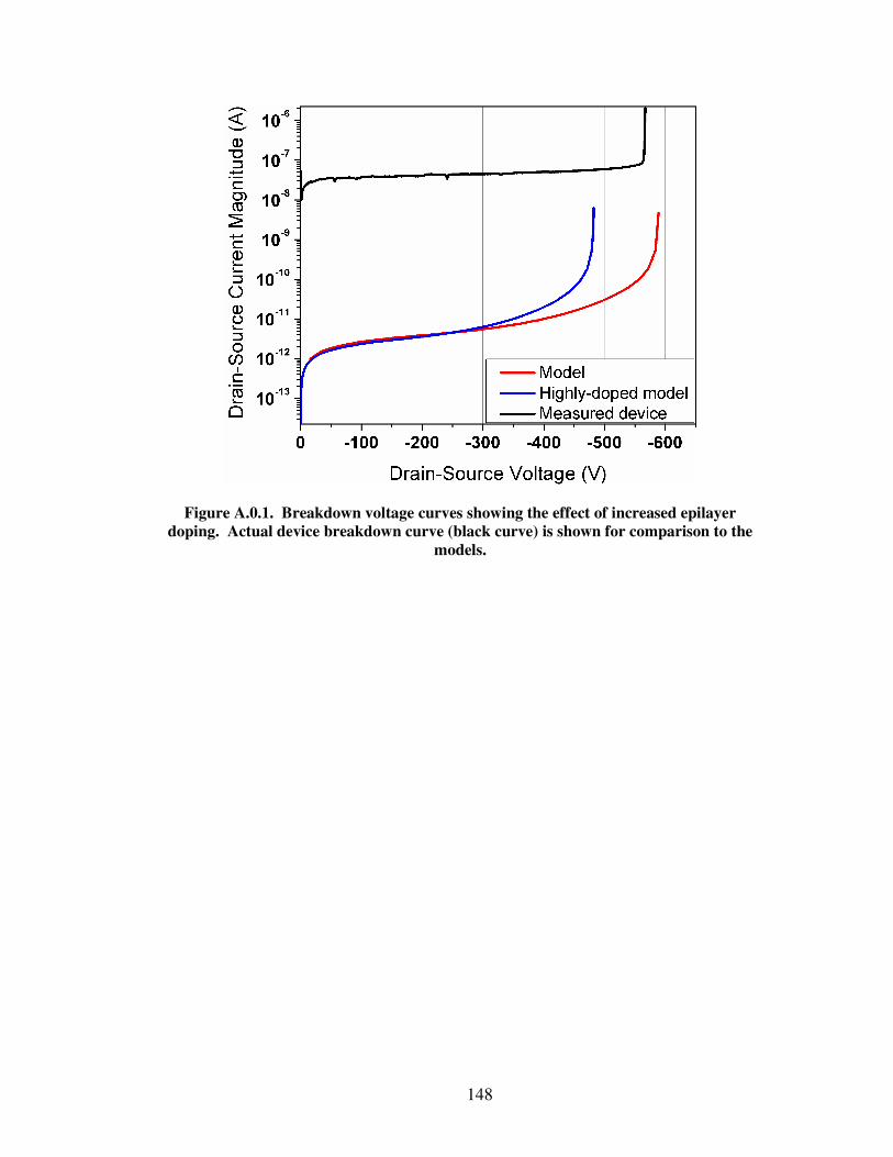
148
Figure A.0.1. Breakdown voltage curves showing the effect of increased epilayer
doping. Actual device breakdown curve (black curve) is shown for comparison to the
models.
149
Bibliography
[1] B. J. Baliga, Power semiconductor devices. Boston: PWS Pub. Co., 1996.
[2] L. E. Selva, G. M. Swift, W. A. Taylor, and L. D. Edmonds, "On the role of energy deposition in triggering SEGR in power MOSFETs," Nuclear Science,
IEEE Transactions on, vol. 46, pp. 1403-1409, 1999.
[3] J. L. Titus, L. S. Jamiolkowski, and C. F. Wheatley, "Development of cosmic ray hardened power MOSFET's," Nuclear Science, IEEE Transactions on,
vol. 36, pp. 2375-2382, 1989.
[4] B. J. Baliga, Fundamentals of Power Semiconductor Devices. New York: Springer Science + Business Media, LLC, 2008.
[5] A. Murray, H. Davis, J. Cao, K. Spring, and T. McDonald, "New power MOSFET technology with extreme ruggedness and ultra-low Rds(on) qualified to Q101 for automotive applications," International Rectifier Corporation White Paper. www.irf.com/technical-info/whitepaper/q101fets.pdf.
[6] G. J. Brucker, P. Measel, D. Oberg, J. Wert, and T. Criswell, "SEU Sensitivity of Power Converters with MOSFETs in Space," Nuclear Science, IEEE
Transactions on, vol. 34, pp. 1792-1795, 1987.
[7] M. R. Patel, Spacecraft power systems. Boca Raton: CRC Press, 2005.
[8] S. Bourdarie and M. Xapsos, "The Near-Earth Space Radiation Environment," Nuclear Science, IEEE Transactions on, vol. 55, pp. 1810-1832, 2008.
[9] A. S. Jursa, Handbook of geophysics and the space environment. Springfield, Va.: Air Force Geophysics Laboratory, Air Force Systems Command National Technical Information Service [distributor], 1985.
[10] M. Xapsos, "Modeling the Space Radiation Environment and Effects on Microelectronic Devices and Circuits, Section II: Modeling the Space Radiation Environment," Ponte Vedra Beach, FL, Proc. 2006 IEEE NSREC Short Course, July 17, 2006.
[11] P. Buehler, "Radiation Belts," in Proceedings of the ESA Workshop on Space
Weather, ESA WPP-155, Noordwijk, The Netherlands, November 11-13, 1998.

150
[12] J. R. Schwank, "Radiation Effects in Commercial Electronics, Section II: Basic Mechanisms of Radiation Effects in the Natural Space Radiation Environment," Tucson, AZ, Proc. 1994 IEEE NSREC Short Course, July 18, 1994.
[13] A. G. Holmes-Siedle and L. Adams, Handbook of radiation effects, 2nd ed. Oxford ; New York: Oxford University Press, 2002.
[14] C. Leroy and P.-G. Rancoita, "Particle interaction and displacement damage in silicon devices operated in radiation environments," Reports on Progress in
Physics, vol. 70, pp. 493-625, 2007.
[15] G. C. Messenger, "A summary review of displacement damage from high energy radiation in silicon semiconductors and semiconductor devices," Nuclear Science, IEEE Transactions on, vol. 39, pp. 468-473, 1992.
[16] M. J. Beck, B. R. Tuttle, R. D. Schrimpf, D. M. Fleetwood, and S. T. Pantelides, "Atomic Displacement Effects in Single-Event Gate Rupture," Nuclear Science, IEEE Transactions on, vol. 55, pp. 3025-3031, 2008.
[17] A. Holmes-Siedle and L. Adams, Handbook of radiation effects, 2nd ed. New York: Oxford University Press, 2002.
[18] T. R. Oldham and F. B. McLean, "Total ionizing dose effects in MOS oxides and devices," Nuclear Science, IEEE Transactions on, vol. 50, pp. 483-499, 2003.
[19] T. R. Oldham, "Recombination along the tracks of heavy charged particles in SiO[sub 2] films," Journal of Applied Physics, vol. 57, pp. 2695-2702, 1985.
[20] L. Onsager, "Initial Recombination of Ions," Physical Review, vol. 54, p. 554, 1938.
[21] R. C. Hughes, "Hole mobility and transport in thin SiO[sub 2] films," Applied
Physics Letters, vol. 26, pp. 436-438, 1975.
[22] C. Kittel, Introduction to solid state physics / Charles Kittel, 8th ed. New York :: Wiley, 2004.
[23] T. R. Oldham and F. B. McLean, "Total ionizing dose effects in MOS oxides and devices," IEEE Transactions on Nuclear Science, vol. 50, pp. 483-499, June 2003 2003.
[24] J. R. Schwank, "Basic mechanisms of radiation effects in the natural space environment," in IEEE Nuclear and Space Radiation Effects Conference Short
Course, Tucson, AZ, 1994, pp. II-1 - II-109.

151
[25] R. D. Schrimpf, P. J. Wahle, R. C. Andrews, D. B. Cooper, and K. F. Galloway, "Dose-rate effects on the total-dose threshold-voltage shift of power MOSFETs," Nuclear Science, IEEE Transactions on, vol. 35, pp. 1536-1540, 1988.
[26] D. L. Blackburn, J. M. Benedetto, and K. F. Galloway, "The Effect of Ionizing Radiation on the Breakdown Voltage of Power MOSFETS," Nuclear
Science, IEEE Transactions on, vol. 30, pp. 4116-4121, 1983.
[27] R. D. Pugh, A. H. Johnston, and K. F. Galloway, "Characteristics of the Breakdown Voltage of Power MOSFETs after Total Dose Irradiation," Nuclear Science, IEEE Transactions on, vol. 33, pp. 1460-1464, 1986.
[28] JEDEC, "References and Terms and Definitions for Radiation Hardness Assurance," in preperation, 2009.
[29] T. A. Fischer, "Heavy-Ion-Induced, Gate-Rupture in Power MOSFETs," Nuclear Science, IEEE Transactions on, vol. 34, pp. 1786-1791, 1987.
[30] T. F. Wrobel, "On Heavy Ion Induced Hard-Errors in Dielectric Structures," Nuclear Science, IEEE Transactions on, vol. 34, pp. 1262-1268, 1987.
[31] M. Allenspach, J. R. Brews, I. Mouret, R. D. Schrimpf, and K. F. Galloway, "Evaluation of SEGR threshold in power MOSFETs," Nuclear Science, IEEE
Transactions on, vol. 41, pp. 2160-2166, 1994.
[32] M. Allenspach, C. Dachs, G. H. Johnson, R. D. Schrimpf, E. Lorfevre, J. M. Palau, J. R. Brews, K. F. Galloway, J. L. Titus, and C. F. Wheatley, "SEGR and SEB in n-channel power MOSFETs," Nuclear Science, IEEE
Transactions on, vol. 43, pp. 2927-2931, 1996.
[33] G. Busatto, A. Porzio, F. Velardi, F. Iannuzzo, A. Sanseverino, and G. Curro, "Experimental and Numerical investigation about SEB/SEGR of Power MOSFET," Microelectronics and Reliability, vol. 45, pp. 1711-1716, 2005.
[34] G. H. Johnson, K. F. Galloway, R. D. Schrimpf, J. L. Titus, C. F. Wheatley, M. Allenspach, and C. Dachs, "A physical interpretation for the single-event-gate-rupture cross-section of n-channel power MOSFETs," Nuclear Science,
IEEE Transactions on, vol. 43, pp. 2932-2937, 1996.
[35] J. L. Titus and C. F. Wheatley, "Experimental studies of single-event gate rupture and burnout in vertical power MOSFETs," Nuclear Science, IEEE
Transactions on, vol. 43, pp. 533-545, 1996.
[36] J. L. Titus, C. F. Wheatley, D. I. Burton, I. Mouret, M. Allenspach, J. Brews, R. Schrimpf, K. Galloway, and R. L. Pease, "Impact of oxide thickness on SEGR failure in vertical power MOSFETs; development of a semi-empirical

152
expression," Nuclear Science, IEEE Transactions on, vol. 42, pp. 1928-1934, 1995.
[37] C. F. Wheatley, J. L. Titus, D. I. Burton, and D. R. Carley, "SEGR response of a radiation-hardened power MOSFET technology," Nuclear Science, IEEE
Transactions on, vol. 43, pp. 2944-2951, 1996.
[38] J. R. Brews, M. Allenspach, R. D. Schrimpf, K. F. Galloway, J. L. Titus, and C. F. Wheatley, "A conceptual model of a single-event gate-rupture in power MOSFETs," Nuclear Science, IEEE Transactions on, vol. 40, pp. 1959-1966, 1993.
[39] M. N. Darwish, M. A. Shibib, M. R. Pinto, and J. L. Titus, "Single event gate rupture of power DMOS transistors," in Electron Devices Meeting, 1993.
IEDM '93. Technical Digest., International, 1993, pp. 671-674.
[40] N. Boruta, G. K. Lum, H. O'Donnell, L. Robinette, M. R. Shaneyfelt, and J. R. Schwank, "A new physics-based model for understanding single-event gate rupture in linear devices," Nuclear Science, IEEE Transactions on, vol. 48, pp. 1917-1924, 2001.
[41] J. L. Titus, C. F. Wheatley, K. M. Van Tyne, J. F. Krieg, D. I. Burton, and A. B. Campbell, "Effect of ion energy upon dielectric breakdown of the capacitor response in vertical power MOSFETs," Nuclear Science, IEEE Transactions
on, vol. 45, pp. 2492-2499, 1998.
[42] M. J. Beck, Y. S. Puzyrev, N. Sergueev, K. Varga, R. D. Schrimpf, D. M. Fleetwood, and S. T. Pantelides, "The Role of Atomic Displacements in Ion-Induced Dielectric Breakdown," Nuclear Science, IEEE Transactions on, vol. 56, pp. 3210-3217, 2009.
[43] A. A. Milgram, "Ion-induced electrical breakdown in metal-oxide-silicon capacitors," Journal of Applied Physics, vol. 67, pp. 1461-1470, 1990.
[44] G. Busatto, G. Currò, F. Iannuzzo, A. Porzio, A. Sanseverino, and F. Velardi, "Experimental study about gate oxide damages in patterned MOS capacitor irradiated with heavy ions," Microelectronics Reliability, vol. 49, pp. 1033-1037, 2009.
[45] G. K. Lum, N. Boruta, J. M. Baker, L. Robinette, M. R. Shaneyfelt, J. R. Schwank, P. E. Dodd, and J. A. Felix, "New experimental findings for single-event gate rupture in MOS capacitors and linear devices," Nuclear Science,
IEEE Transactions on, vol. 51, pp. 3263-3269, 2004.
[46] J. L. Titus, S. Yen-Sheng, M. W. Savage, R. V. Mickevicius, and C. F. Wheatley, "Simulation study of single-event gate rupture using radiation-hardened stripe cell power MOSFET structures," Nuclear Science, IEEE
Transactions on, vol. 50, pp. 2256-2264, 2003.

153
[47] "Test Methods for Semiconductor Devices," United States Department of Defense, Nov, 2006.
[48] K. Sahu, "EEE-INST-002: Instructions for EEE Parts Selection, Screening, Qualification,and Derating," NASA/TP-2003-212242, 2003.
[49] L. Scheick and L. Selva, "Sensitivity to LET and Test Conditions for SEE Testing of Power MOSFETs," in 2009 IEEE Radiation Effects Data
Workshop, 2009, pp. 82-93.
[50] J. L. Titus and C. F. Wheatley, "SEE characterization of vertical DMOSFETs: an updated test protocol," Nuclear Science, IEEE Transactions on, vol. 50, pp. 2341-2351, 2003.
[51] J. L. Titus, C. F. Wheatley, M. Allenspach, R. D. Schrimpf, D. I. Burton, J. R. Brews, K. F. Galloway, and R. L. Pease, "Influence of ion beam energy on SEGR failure thresholds of vertical power MOSFETs," Nuclear Science,
IEEE Transactions on, vol. 43, pp. 2938-2943, 1996.
[52] A. J. Tylka, J. H. Adams, Jr., P. R. Boberg, B. Brownstein, W. F. Dietrich, E. O. Flueckiger, E. L. Petersen, M. A. Shea, D. F. Smart, and E. C. Smith, "CREME96: A Revision of the Cosmic Ray Effects on Micro-Electronics Code," Nuclear Science, IEEE Transactions on, vol. 44, pp. 2150-2160, 1997.
[53] J. L. Titus, C. F. Wheatley, T. H. Wheatley, W. A. Levinson, D. I. Burton, J. L. Barth, R. A. Reed, K. A. LaBel, J. W. Howard, and K. M. van Tyne, "Prediction of early lethal SEGR failures of VDMOSFETs for commercial space systems'," Nuclear Science, IEEE Transactions on, vol. 46, pp. 1640-1651, 1999.
[54] L. Z. Scheick and L. E. Selva, "Effect of Dose History on SEGR Properties of Power MOSFETS," Nuclear Science, IEEE Transactions on, vol. 54, pp. 2568-2575, 2007.
[55] J. JESD57, "Test Procedure for the Management of Single-Event Effects in Semiconductor Devices from Heavy Ion Radiation (JC-13.4)," EWJEDEC, 2500 Wilson Blvd, Arlington, VA, 22201-3834, 1996.
[56] L. E. Selva, L. Z. Scheick, S. McClure, T. Miyahira, S. M. Guertin, S. K. Shah, L. D. Edmonds, and J. D. Patterson, "Catastrophic SEE in high-voltage power MOSFETs," 2003, pp. 113-120.
[57] J. L. Titus, C. F. Wheatley, J. E. Gillberg, and D. I. Burton, "A study of ion energy and its effects upon an SEGR-hardened stripe-cell MOSFET technology [space-based systems]," Nuclear Science, IEEE Transactions on,
vol. 48, pp. 1879-1884, 2001.

154
[58] S. Liu, "Worst-Case Test Conditions of SEGR for Power DMOSFETs," Nuclear Science, IEEE Transactions on, vol. 57, pp. 279-287, 2010.
[59] Synopsys, Sentaurus Device User Guide: Synopsys Inc, 700 East Middlefield Rd, Mountain View, CA 94043, 2007.
[60] J. L. Titus, "Test Report: Microsemi Power MOSFET (MSAFX11P50A) (Single Event Effects/Survivability)," http://radhome.gsfc.nasa.gov/radhome/papers/T021907_MSAFX11P50A.pdf Mar 2007 2007.
[61] J. F. Ziegler and J. P. Biersack, "The Stopping and Range of Ions in Matter," http://www.srim.org.
[62] O. Fageeha, J. Howard, and R. C. Block, "Distribution of radial energy deposition around the track of energetic charged particles in silicon," Journal
of Applied Physics, vol. 75, pp. 2317-2321, 1994.
[63] C. F. Wheatley, J. L. Titus, and D. I. Burton, "Single-event gate rupture in vertical power MOSFETs; an original empirical expression," Nuclear Science,
IEEE Transactions on, vol. 41, pp. 2152-2159, 1994.
[64] R. J. Larsen, M. L. Marx, and B. Cooil, Statistics for Applied Problem Solving
and Decision Making. Albany: Duxbury Press, 1997.
[65] S. Liu, private communication, Jan 2011.
[66] D. McMorrow, W. T. Lotshaw, J. S. Melinger, S. P. Buchner, and R. L. Pease, "Subbandgap Laser-Induced Single Event Effects: Carrier Generation via Two-Photon Absorption," Ieee Transactions on Nuclear Science, vol. 49, pp. 3002-3008, 2002.
[67] S. Liu, J. M. Lauenstein, V. Ferlet-Cavrois, R. Marec, F. Hernandez, L. Scheick, F. Bezerra, N. Sukhaseum, L. Coquelet, M. Muschitiello, H. Cao, D. Carrier, M. Brisbois, R. Mangeret, R. Ecoffet, K. A. LaBel, M. Zafrani, and P. Sherman, "Effects of Ion Species on SEB Failure Voltage of Power DMOSFET," to be presented, IEEE Nuclear and Space Radiation Effects
Conference Las Vegas, NV, July 25-29, 2011.
[68] P. F. Peyrard, T. Beutier, O. Serres, C. Chatry, R. Ecoffet, G. Rolland, D. Boscher, S. Bourdarie, C. Inguimbert, P. Calvel, and R. Mangeret, "A toolkit for space environment," in Radiation and Its Effects on Components and
Systems, 2003. RADECS 2003. Proceedings of the 7th European Conference
on, 2003, pp. 639-641.
[69] P. R. Bevington, Data Reduction and Error Analysis for the Physical
Sciences. New York: McGraw-Hill, 1969.

155
[70] R. Ladbury, "Statistical Properties of SEE Rate Calculation in the Limits of Large and Small Event Counts," Nuclear Science, IEEE Transactions on, vol. 54, pp. 2113-2119, 2007.
[71] D. S. Sivia and J. Skilling, Data Analysis: A Bayesian Tutorial, 2nd ed. New York: Oxford University Press, 2006.
[72] ISO_15390:2004, "Space environment (natural and artificial) -- Galactic cosmic ray model," Geneva, Switzerland: ISO, 2004.
[73] http://www.irf.com/product-info/hi-rel/radhard.html.
[74] J. R. Srour, C. J. Marshall, and P. W. Marshall, "Review of displacement damage effects in silicon devices," Nuclear Science, IEEE Transactions on,
vol. 50, pp. 653-670, 2003.
[75] D. L. Blackburn, T. C. Robbins, and K. F. Galloway, "VDMOS Power Transistor Drain-Source Resistance Radiation Dependence," Nuclear Science,
IEEE Transactions on, vol. 28, pp. 4354-4359, 1981.
[76] F. Faccio, B. Allongue, G. Blanchot, C. Fuentes, S. Michelis, S. Orlandi, and R. Sorge, "TID and Displacement Damage Effects in Vertical and Lateral Power MOSFETs for Integrated DC-DC Converters," Nuclear Science, IEEE
Transactions on, vol. 57, pp. 1790-1797, 2010.
[77] A. Candelori, M. Ceschia, A. Paccagnella, J. Wyss, D. Bisello, and G. Ghidini, "Thin oxide degradation after high-energy ion irradiation," Nuclear
Science, IEEE Transactions on, vol. 48, pp. 1735-1743, 2001.
[78] M. Lenzlinger and E. H. Snow, "Fowler-Nordheim Tunneling into Thermally Grown SiO[sub 2]," Journal of Applied Physics, vol. 40, pp. 278-283, 1969.
[79] J. M. McGarrity, "Considerations for Hardening MOS Devices and Circuits for Low Radiation Doses," Nuclear Science, IEEE Transactions on, vol. 27, pp. 1739-1744, 1980.
[80] J. R. Srour and K. Y. Chiu, "MOS Hardening Approaches for Low-Temperature Applications," Nuclear Science, IEEE Transactions on, vol. 24, pp. 2140-2146, 1977.
[81] T. R. Oldham, Ionizing Radiation Effects in MOS Oxides. River Edge, NJ: World Scientific Publishing Col, 1999.
[82] N. S. Saks, M. G. Ancona, and J. A. Modolo, "Radiation Effects in MOS Capacitors with Very Thin Oxides at 80°K," Nuclear Science, IEEE
Transactions on, vol. 31, pp. 1249-1255, 1984.
156
[83] P. S. Winokur, "Radiation-Induced Interface Traps," in Ionizing Radiation
Effects in MOS Devices and Circuits, T. P. Ma and P. V. Dressendorfer, Eds. New York: John Wiley and Sons, Inc., 1989, pp. 193-255.
[84] P. J. McWhorter and P. S. Winokur, "Simple Technique for Separating the Effects of Interface Traps and Trapped-Oxide Charge in Metal-Oxide-Semiconductor Transistors," Applied Physics Letters, vol. 48, pp. 133-135, 1986.
[85] A. Haran, M. Murat, and J. Barak, "Charge yield and track structure effects on total ionizing dose measurements," Ieee Transactions on Nuclear Science, vol. 55, pp. 2098-2105, 2008.
[86] J. A. Felix, M. R. Shaneyfelt, J. R. Schwank, S. M. Dalton, P. E. Dodd, and J. B. Witcher, "Enhanced degradation in power MOSFET devices due to heavy ion irradiation," Ieee Transactions on Nuclear Science, vol. 54, pp. 2181-2189, Dec 2007.
[87] M. R. Shaneyfelt, J. A. Felix, P. E. Dodd, J. R. Schwank, S. M. Dalton, J. Baggio, V. Ferlet-Cavrois, P. Paillet, and E. W. Blackmore, "Enhanced Proton and Neutron Induced Degradation and Its Impact on Hardness Assurance Testing," Nuclear Science, IEEE Transactions on, vol. 55, pp. 3096-3105, 2008.
[88] D. Grafham, "Improved Power MOSFETs Boost Efficiency in a 3.5kW Single Phase PFC," Advanced Power Technology Application Note APT0101, 2001.
[89] D. A. Grant and J. Gowar, Power MOSFETS : theory and applications. New York: Wiley, 1989.
[90] M. Murat, A. Akkerman, and J. Barak, "Ion Track Structure and Dynamics in SiO2," Nuclear Science, IEEE Transactions on, vol. 55, pp. 2113-2120, 2008.
[91] A. Akkerman and J. Barak, "Ion-track structure and its effects in small size volumes of silicon," Nuclear Science, IEEE Transactions on, vol. 49, pp. 3022-3031, 2002.
[92] "Space Product Assurance: Radiation Hardness Assurance," European Space Agency, ESA-TEC-QE/2009/22. Issue 1, May, 2009.
[93] R. C. Hughes, "High field electronic properties of SiO2," Solid-State
Electronics, vol. 21, pp. 251-258, 1978.
[94] T. R. Oldham, "Charge Generation and Recombination in Silicon Dioxide from Heavy Charged Particles," Harry Diamond Laboratories, Adelphi, MD, HDL-TR-1985, April 1982.

157
[95] S. R. Anderson, R. D. Schrimpf, K. F. Galloway, and J. L. Titus, "Exploration of Heavy Ion Irradiation Effects on Gate Oxide Reliability in Power MOSFETs," Microelectronics and Reliability, vol. 35, pp. 603-608, 1995.
[96] F. W. Sexton, D. M. Fleetwood, M. R. Shaneyfelt, P. E. Dodd, G. L. Hash, L. P. Schanwald, R. A. Loemker, K. S. Krisch, M. L. Green, B. E. Weir, and P. J. Silverman, "Precursor Ion Damage and Angular Dependence of Single Event Gate Rupture in Thin Oxides," Ieee Transactions on Nuclear Science, vol. 45, pp. 2509-2517, 1998.
[97] S. R. Messenger, E. A. Burke, M. A. Xapsos, G. P. Summers, R. J. Walters, J. Insoo, and T. Jordan, "NIEL for heavy ions: an analytical approach," Nuclear
Science, IEEE Transactions on, vol. 50, pp. 1919-1923, 2003.
[98] M. A. Xapsos, E. A. Burke, F. F. Badavi, L. W. Townsend, J. W. Wilson, and I. Jun, "NIEL Calculations for High-Energy Heavy Ions," Ieee Transactions
on Nuclear Science, vol. 51, pp. 3250-3254, 2004.
[99] D. Jiles, Introduction to the Electronic Properties of Materials, 2nd ed. Cheltenham, UK: Nelson Thornes Ltd., 2001.
[100] R. E. Newnham, Properties of Materials: Anisotropy, Symmetry, Structure. New York: Oxford University Press inc., 2005.
[101] L. W. Massengill, B. K. Choi, D. M. Fleetwood, R. D. Schrimpf, K. F. Galloway, M. R. Shaneyfelt, T. L. Meisenheimer, P. E. Dodd, J. R. Schwank, R. S. Johnson, and G. Lucovsky, "Heavy-Ion-Induced Breakdown in Ultra-Thin Gate Oxides and High-k Dielectrics," Ieee Transactions on Nuclear
Science, vol. 48, pp. 1904-1912, 2001.