
00 rd 33 Annual Children's Fishing Tournament Cosponsored ...

About the Nanoscale Science, Engineering, and Technology Subcommittee
The Nanoscale Science, Engineering, and Technology (NSET) Subcommittee is the interagency body responsible for coordinating, planning, implementing, and reviewing the National Nanotechnology Initiative. The NSET Subcommittee was established in 2000, replacing the Interagency Working Group on Nanoscience, Engineering, Technology (IWGN), which was formed in 1998. NSET is a subcommittee of the National Science and Technology Council (NSTC), which is one of the principal means by which the President coordinates science, space, and technology policies across the Federal Government. The National Nanotechnology Coordination Office (NNCO) provides technical and administrative support to the NSET Subcommittee and supports the subcommittee in the preparation of multi-agency planning, budget, and assessment documents, including this report.
For more information on NSET, see http://www.nano.gov/html/about/nsetmembers.html.
For more information on NSTC, see http://www.ostp.gov/NSTC/html/NSTC_Home.html.
For more information on the NNI, NSET, and NNCO, see http://www.nano.gov.
About this document
This document is the report of a workshop held under NSET auspices in March 2004 aimed at identifying and articulating the relationship of nanoscale science and technology to the Nation’s energy future. The report also addresses the Grand Challenge in Energy Conversion and Storage set out in the National Nanotechnology Initiative (NNI) Supplement to the President’s FY 2004 Budget. It also was used as input for the NNI Strategic Plan released in December 2004. The meeting was jointly sponsored by the U.S. Department of Energy and, through the NNCO, the other member agencies of the NSET Subcommittee.
Cover and book design
Book design by Patricia Yalden and other staff members at Brookhaven National Laboratory. Cover design by Kanako Yamamoto of Affordable Creative Services, Inc.
Front cover: Scanning tunneling microscope image of an ammonia synthesis catalyst that is made of ruthenium particles about 10 nanometers in diameter. This nanoparticle catalyst is 10 times more active than commercial iron-based catalysts (courtesy of Zhen Song and Jan Hrbek, Brookhaven National Laboratory).
Back cover: Detailed atomic structure of silicon nanoparticles simulated by state-of-the-art, highly accurate quantum techniques (courtesy of Giulia Galli, Lawrence Livermore National Laboratory). (Figures © 2003 American Physical Society; reprinted by permission. See sidebar on p. 47 and reference 51 on p. 64 for more information.)
Background graphic at bottom of entire cover courtesy of L.J. Whitman, Naval Research Laboratory.
Copyright information
This document is a work of the U.S. Government and is in the public domain. Subject to stipulations below, it may be distributed and copied, with acknowledgment to the National Nanotechnology Coordination Office (NNCO) and the U.S. Department of Energy. Copyrights to portions of this report (including graphics) contributed by workshop participants and others are reserved by original copyright holders or their assignees, and are used here under the Government’s license and by permission. Requests to use any images must be made to the provider identified in the image credits, or to the NNCO if no provider is identified.
Printed in the United States of America. Second edition, 2005.

Principal Authors
Nanoscience Research for Energy Needs
Report of the March 2004 National Nanotechnology Initiative Grand Challenge Workshop
Second Edition, June 2005
Paul Alivisatos University of California, Berkeley and
Lawrence Berkeley National Laboratory
Peter Cummings Vanderbilt University and
Oak Ridge National Laboratory
James De Yoreo Lawrence Livermore National Laboratory
Kristen Fichthorn Pennsylvania State University
Bruce Gates University of California, Davis
Robert Hwang Brookhaven National Laboratory
Douglas Lowndes Oak Ridge National Laboratory
Arun Majumdar University of California, Berkeley
Lee Makowski Argonne National Laboratory
Terry Michalske Sandia National Laboratories
James Misewich Brookhaven National Laboratory
Cherry Murray Lucent Technologies
Steve Sibener University of Chicago
Clayton Teague National Nanotechnology Coordinating Office
Ellen Williams University of Maryland
Sponsored by
National Science and Technology Council
Committee on TechnologySubcommittee on Nanoscale Science, Engineering, and Technology
Department of EnergyOffice of Basic Energy Sciences

Acknowledgments
Thanks are extended to the principal authors listed on the title page of this report (reverse side of this page). In addition, the report’s authors wish to thank all the participants at the March 16–18, 2004 workshop held in Arlington, VA, particularly the workshop cochairs, Ellen Williams of the University of Maryland and Robert Hwang of Brookhaven National Laboratory. The presentations and discussions at that workshop provided the foundation for this report.
Credit is due to staff members in the Department of Energy’s Office of Basic Energy Sciences and in the National Nanotechnology Coordination Office who assisted in organizing the workshop and in editing the final report:
Christie Ashton, Department of Energy’s Office of Basic Energy Sciences Sam Gill, NNCO Stephen Gould, NNCO Geoffrey Holdridge, NNCO Philip Lippel, NNCO
Special thanks are due to Robert Hwang and other staff members at Brookhaven National Laboratory who prepared, edited, and printed the first edition of the manuscript, and to Geoffrey Holdridge, Philip Lippel, Cate Alexander, and other staff members at the National Nanotechnology Coordination Office and WTEC, Inc. who contributed to editing, production, and distribution of this second edition.
Finally, thanks to all the members of the National Science and Technology Council’s Subcommittee on Nanoscale Science, Engineering, and Technology, who cosponsored the workshop with the Department of Energy and who reviewed the draft report before its publication.
This workshop was sponsored by the U.S. Department of Energy and, through the National Nanotechnology Coordination Office, the other member agencies of the Nanoscale Science, Engineering, and Technology (NSET) Subcommittee, Committee on Technology, National Science and Technology Council. Any opinions, findings, and conclusions or recommendations expressed in this material are those of the authors and do not necessarily reflect the views of the United States Government or the authors’ parent institutions.
iNanoscience Research for Energy Needs
Preface
This report on Nanoscience Research for Energy Needs is one of a series of reports resulting from workshops convened over the last 18 months by the Nanoscale Science, Engineering, and Technology (NSET) Subcommittee of the National Science and Technology Council’s Committee on Technology. The workshops were part of the NSET Subcommittee’s long-range planning effort for the National Nanotechnology Initiative (NNI), the multi-agency Federal nanotechnology program. The NNI is driven by long-term goals based on broad community input, in part received through these workshops. The NNI seeks to accelerate the research, development, and deployment of nanotechnology to address national needs, enhance our nation’s economy, and improve the quality of life in the United States and around the world, through coordination of activities and programs across the Federal government.
One major component of the NNI is collectively known as the “Grand Challenges.” This NNI component focuses on research and development (R&D) areas with visionary goals that are directly related to applications of nanotechnology and that have been identified as having the potential to realize significant economic, governmental, and societal impact. The nine grand challenge areas are
• Nanostructured Materials by Design
• Manufacturing at the Nanoscale
• Chemical-Biological-Radiological-Explosive Detection and Protection
• Nanoscale Instrumentation and Metrology
• Nano-Electronics, -Photonics, and -Magnetics
• Healthcare, Therapeutics, and Diagnostics
• Nanoscience Research for Energy Needs
• Microcraft and Robotics
• Nanoscale Processes for Environmental Improvement
The NSET Subcommittee convened a workshop on each Grand Challenge topic to obtain broad input on the state of current research and long-term challenges and goals. Nanotechnology experts from industry, academia, and government were asked to (1) develop broad, long-term (10 years or longer), visionary goals within the Grand Challenge area and (2) identify specific scientific and technological barriers—or “hard problems”—that once overcome will enable “quantum advances” toward those goals. This workshop report addresses the grand challenge topic on nanoscience research for energy needs.
The resulting workshop reports will inform the respective professional communities, as well as various organizations that have responsibilities for coordinating, implementing, and guiding the NNI. The reports also will provide direction to researchers and program managers in specific areas of nanotechnology R&D regarding long-term goals and hard problems. This report identifies nine important areas for energy-related research where nanoscale science and engineering promises large implications, from hydrogen and solar energy production to new generations of fuel cells and efficient electric transmission lines. The scope of this workshop did not cover the topic of nanotechnology in energetic materials such as propellants and explosives.

Nanoscience Research for Energy Needsii
Preface
On behalf of the NSET Subcommittee, we wish to thank Drs. Robert Hwang and Ellen Williams for their creativity and hard work in conducting an outstanding workshop and in preparing this report. We also thank all the speakers, session chairs, and participants for their time and efforts to join the workshop and to make their individual contributions to the discussions at the workshop and then to draft this report. Their generous sharing of their research results and their insights ensures that this document will serve as a reference for the NNI.
Mihail C. Roco E. Clayton Teague Chair, Nanoscale Science, Engineering, Director, National Nanotechnology and Technology Subcommittee Coordination Office

iiiNanoscience Research for Energy Needs
Table of Contents
Preface ......................................................................................................................... i
Table of Contents ......................................................................................................iii
Executive Summary .................................................................................................. v
1. Introduction .......................................................................................................... 1
2. Research Targets in Nanoscience for Energy Needs ......................................... 3
3. Crosscutting Themes
Catalysis by Nanoscale Materials ........................................................................ 13
Using Interfaces to Manipulate Energy Carriers .................................................. 19
Linking Structure and Function at the Nanoscale ................................................ 30
Assembly and Architecture .................................................................................. 36
Theory, Modeling, and Simulation for Energy Nanoscience ............................... 44
Scalable Synthesis ................................................................................................ 51
References ............................................................................................................ 62
Appendix A. Workshop Agenda ............................................................................ 67
Appendix B. List of Participants ........................................................................... 69

iv Nanoscience Research for Energy Needs

vNanoscience Research for Energy Needs
Executive Summary
The world demand for energy is expected to double to 28 terawatts by the year 2050. Compounding this challenge is the growing need to protect our environment by increasing energy efficiency and developing “clean” energy sources. These are indeed global challenges, and their resolution is vital to our energy security. Recent reports on Basic Research Needs to Assure a Secure Energy Future (Department of Energy, Basic Energy Sciences Advisory Committee) and Basic Research Needs for the Hydrogen Economy (DOE, Office of Basic Energy Sciences) have recognized that solutions will require scientific breakthroughs and truly revolutionary developments. Within this context, nanoscience and nanotechnology present exciting and requisite approaches to addressing these challenges.
ABOUT THE WORKSHOP
An interagency workshop to identify and articulate the relationship of nanoscale science and technology to the nation’s energy future was convened on March 16 -18, 2004, in Arlington, Virginia. The meeting was jointly sponsored by the Department of Energy and, through the National Nanotechnology Coordination Office, the other member agencies of the Nanoscale Science, Engineering, and Technology Subcommittee of the Committee on Technology, National Science and Technology Council (NSTC). This report is the outcome of that workshop.
The workshop participants included 63 invited presenters, among them 32 from universities, 26 from national laboratories, and 5 from industry. This workshop was one in a series intended to provide input from the research community on the next National Nanotechnology Initiative (NNI) Strategic Plan that NSTC delivered to Congress in December 2004, as called for in the 21st Century Nanotechnology Research and Development Act.
At the root of the opportunities provided by nanoscience to enhance our energy security is the fact that all of the elementary steps of energy conversion (e.g., charge transfer, molecular rearrangement, chemical reactions, etc.) take place on the nanoscale. Thus, the development of new nanoscale materials, as well as the methods to characterize, manipulate, and assemble them, creates an entirely new paradigm for developing new and revolutionary energy technologies. The primary outcome of the workshop was the identification of nine research targets in energy-related science and technology in which nanoscience is expected to have the greatest impact:
1. Scalable methods to split water with sunlight for hydrogen production
2. Highly selective catalysts for clean and energy-efficient manufacturing
3. Harvesting solar energy with 20% power efficiency and 100 times lower cost
4. Solid-state lighting at 50% of the present power consumption
5. Super-strong, lightweight materials to improve efficiency of cars, airplanes, and the like
6. Reversible hydrogen storage materials operating at ambient temperatures
7. Power transmission lines capable of 1 gigawatt transmission
Nanoscience Research for Energy Needsvi
Executive Summary
8. Low-cost fuel cells, batteries, thermoelectrics, and ultra-capacitors built from nanostructured materials
9. Materials synthesis and energy harvesting based on the efficient and selective mechanisms of biology
The report contains descriptions of many examples indicative of outcomes and expected progress in each of these research targets. For successful achievement of these research targets, participants recognized six foundational and vital crosscutting nanoscience research themes:
1. Catalysis by nanoscale materials
2. Using interfaces to manipulate energy carriers
3. Linking structure and function at the nanoscale
4. Assembly and architecture of nanoscale structures
5. Theory, modeling, and simulation for energy nanoscience
6. Scalable synthesis methods
FOUNDATIONAL RESEARCH THEMES
Catalysis by Nanoscale Materials
Catalysis provides the means of controlling the rates at which chemical bonds are formed and broken, and is the key to energy conversion and environmental protection in chemical manufacturing and transportation. The petroleum, chemical, and pharmaceutical industries that rely on catalysts contribute $500 billion annually to the gross national product of the United States. Nanostructured materials provide an extraordinary opportunity to dramatically improve catalytic performance. For example, gold in its bulk form is known to be chemically inert. However, nanoparticles of gold on a titania substrate exhibit remarkable catalytic properties such as the ability to decompose the environmentally hazardous gas sulfur dioxide. The efficiency of this material is 10 times greater than that of commercial catalysts used today.
The research challenge in nanoscience for catalysis is learning to tune the energy landscape of the chemical reactants as they interact with the nanostructured catalyst materials. Drawing from the lessons of biology, nanostructured materials must be designed to match both the structural conformation of the reactants and to control the reaction pathway to the desired product. To accomplish this, new and efficient methods of in situ characterization and rapid throughput testing of catalytic properties will be required. The choice of materials, structural parameters, and the experimental design must be guided by a continually improving fundamental understanding of the structure-function relationships of the nanostructured catalysts.
Using Interfaces to Manipulate Energy Carriers
The use of engineered nanostructures at interfaces has demonstrated a compelling potential for improving energy security based on advances in efficient power handling, low-power electronics, energy harvesting, and efficient energy use in lighting. The most significant research challenge needed to addressing these issues is to create interfaces that are tailored at the nanoscale to optimize transport of energy in many forms (electrons, phonons, photons, excitons). The possibilities include fabricating interfaces using a wide variety of materials and chemical combinations, along with interface shapes patterned at the nanometer length scale. The crosscutting research challenge will be to use this variability to tailor the

viiNanoscience Research for Energy Needs
Executive Summary
interface functionality for electron transport (electrical transmission, losses, small devices), electron and phonon transport (thermoelectrics), photon collection and electron and exciton transport (photovoltaics), and electron and hole recombination (lighting). To accomplish this, a diverse array of synthesis methods ranging from top-down lithography through self-assembling materials growth, wet-chemical processing, and biological assembly must be combined to create novel structures. In parallel, experimental techniques for nanoscale characterization must be developed and used to relate structure and function.
Linking Structure and Function at the Nanoscale
At the heart of nanoscience are the new phenomena and properties that emerge as materials are constructed at the nanometer scale. These properties originate from the fact that nanoscale materials with individual building blocks consisting of only 100–10,000 atoms have unique structures and behavior that cannot be extrapolated from our understanding of the bulk materials that we routinely use in our lives. The overarching research challenge that we face in designing novel nanomaterials is establishing the physical and chemical principles that determine the functionality that emerges at nanometer length scales, and exploiting this functionality for improved energy security. Effects of quantum confinement, the enhancement of interfacial free energies over bulk free energies, and the importance of surface states have all been recognized since the inception of nanoscience. In addition, there are many effects of nanoscale structure that have only begun to be explored, such as the mechanical properties of nanostructures and fluid-flow in nanoporous structures for which the electric double layer is less than the pore size. Meeting this challenge will involve crosscutting research correlating exploratory synthesis; functional characterization; and theory, modeling, and simulation.
Assembly and Architecture
Exploiting the novel properties of individual nanostructures generally will involve assembling the nanostructures into carefully designed and controlled architectures that amplify or modify their desired functionality. The major research challenge is to predict the properties of assemblies of nanostructures and to devise novel strategies for assembly of these architectures, initially in small quantities, but eventually in bulk. To reach the goal of using nanoscale architectures for energy applications in both the near and long terms, we will need to overcome significant technological barriers. Over the next decade, investment in fundamental studies of the properties of nanostructured materials and the methods for assembling these materials will drive development of methods that will allow
• Prediction of the nanoscale architectures that will achieve extraordinary and novel material properties for energy applications
• Control of the nanoscale architecture to enable the fabrication of structures predicted to exhibit desirable functions
• Development of programmed assembly processes to implement cost-effective fabrication of the structures with predicted functionalities
The final goal of this investment will be engineering architectures that integrate nanoscale capabilities into micro- and macro-scale systems that address energy applications and needs.
Theory, Modeling, and Simulation for Energy Nanoscience
Opportunities in nanoscience and technology encompass a combinatorially large range of solid-state and molecular materials, chemical compositions, interface configurations, and system architectures. Predicting the structure, composition, and architectures that give rise to desirable functional behavior is a major research challenge, which can only be met by using the power of theory, modeling, and

Nanoscience Research for Energy Needsviii
Executive Summary
simulation (TMS). Applications of TMS cut across all of the research challenges of nanoscience for energy applications, with specific potential to guide experimental design and interpretation, predict the impact of dynamics and fluctuations, guide development of self-assembly methods, predict functional behavior including catalytic activity and energy transport mechanisms, and guide the exploration and synthesis of new materials.
Today, the TMS capabilities to meet these needs exist in varying degrees of maturity, with demonstrated potential to develop the expanded power needed for the nanoscience research challenges. Fundamental research in theory, simulation methodologies, and algorithms in a variety of areas have been identified as the key TMS needs for advancing the nation’s future energy security. These include
• Methods for bridging temporal and spatial scales
• Many-body electronic structure calculations
• Electron transport including interfaces
• Electronic structure methods for optical properties
Scalable Synthesis Methods
The ultimate research challenge is to synthesize functional nanomaterials at a practical manufacturing level in a controllable manner. Meeting this challenge is essential for the truly revolutionary subsequent developments that are needed to meet the huge energy challenge that the United States now faces.
The synthesis of nanomaterials involves challenges in the quality, quantity, variety, and integrated design and assembly of nanomaterials. The quality challenge requires synthesizing promising nanomaterials with sufficiently high purity and freedom from defects that their ultimate properties can be reliably measured and accurately known. The quantity challenge requires developing, understanding, and optimizing synthesis methods for economical, large-scale production of nanomaterials. Readily scalable and low-cost methods for producing large quantities of sufficiently high-quality nanomaterials are needed. The variety challenge requires research and development of methods to efficiently explore and expand the library of “building blocks” of enhanced nanomaterial properties that are potentially available for use. The integrated design challenge requires developing synthesis methods that are compatible with the subsequent or concurrent assembly of nanomaterials into systems or architectures that permit their greatly enhanced properties to be expressed at the macroscale.

1Nanoscience Research for Energy Needs
1. Introduction
GLOBAL DRIVERS
The world demand for energy is expected to double from 14 terawatts (TW) in the year 2000 to 28 TW by the year 2050. Driving this need is the expanding world population that is expected to grow to 10 to 11 billion people within that same time frame. Since this population increase will be concentrated in developing countries, it will have an impact not only on energy consumption patterns, but also on the environment (e.g., on greenhouse gas production). These factors compound the energy-need challenge with the growing need to protect our environment, requiring renewed efforts and novel approaches to increasing energy efficiency and developing “clean” energy sources. It is clear that how we address and eventually meet these needs will have broad impact on our standard of living and the national economy. Recent reports on Basic Research Needs to Assure a Secure Energy Future (Department of Energy, Basic Energy Sciences Advisory Committee) and Basic Research Needs for the Hydrogen Economy (DOE, Office of Basic Energy Sciences) have recognized that scientific “breakthroughs and truly revolutionary developments” are demanded. Within this context, nanoscience and nanotechnology offer exciting and requisite approaches to addressing these challenges.
An interagency workshop to identify and articulate the relationship of nanoscale science and technology to the nation’s energy future was convened on March 16–18, 2004, in Arlington, Virginia. The meeting was jointly sponsored by the Department of Energy and, through the National Nanotechnology Coordination Office, the other member agencies of the Nanoscale Science, Engineering, and Technology Subcommittee of the Committee on Technology, National Science and Technology Council. The workshop consisted of 63 participants of whom 32 were from universities, 26 from national laboratories, and 5 from industry. The appendix to this report contains a complete list of participants along with the workshop agenda. This workshop was one in a series intended to provide input from the research community on the NNI Strategic Plan that NSTC delivered to Congress in December 2004, as called for in the 21st Century Nanotechnology Research and Development Act.
OBJECTIVE OF WORKSHOP
The goal of this workshop was to define opportunities and goals in energy-related research for the next decade and to determine the special opportunities that the field of nanoscience affords to energy research. The group was tasked to identify long-term (10 years or more) visionary challenges for researchers in the area of energy-related science and technology that could inform the development of National Nanotechnology Initiative Grand Challenges. Participants discussed and identified research themes and specific “hard problems” that would have the greatest impact in addressing energy needs and the specific scientific and technological hurdles that have to be overcome to achieve broader R&D goals. The group also developed strategies for solving these “hard problems” and identified the necessary scientific infrastructure.
Nanoscience Research for Energy Needs2
1. Introduction
STRUCTURE OF REPORT
The primary outcome of the workshop was the identification of nine research targets in energy-related science and technology in which nanoscience is expected to have primary impact. An overview of these research targets is provided in the following section. Participants identified six foundational crosscutting nanoscience research themes that are vital to the successful achievement of the research targets. Strategies for addressing each of these themes are detailed in subsequent chapters, including statements of the vision, state of the art, major technical challenges, infrastructure needs, and research expectations for the respective research theme. Appendices include a list of participants and the agenda of the workshop. The extended abstracts submitted by the participants in advance of the workshop are provided on a CD/ROM included with the printed version of this report, which is available from the National Nanotechnology Coordination Office.
3Nanoscience Research for Energy Needs
2. Research Targets in Nanoscience for Energy Needs
Energy impacts all aspects of our quality of life and economy. The challenges that face us are, in fact, global, with a complex landscape of implications and drivers. These challenges highlight the crucial importance of technology development and the leadership role of the United States. The recent Department of Energy report on Basic Research Needs to Assure a Secure Energy Future details the global needs and challenges and responsibilities we have in the United States. These are indeed daunting, requiring both short-term and long-term R&D. It is now widely recognized that technology breakthroughs and truly revolutionary developments are needed. It is here that nanoscience and nanotechnology must play a pivotal role.
At the root of the opportunities provided by nanoscience to improve our energy security is the fact that all elementary steps of energy conversion (such as charge transfer, molecular rearrangement, chemical reactions, etc.) take place on the nanoscale. Thus, the development of new nanoscale materials, as well as the methods to characterize, manipulate, and assemble them, creates an entirely new paradigm for developing new and revolutionary energy technologies. Our workshop has identified nine key areas of energy technology in which nanoscience can have the greatest impact. These research targets are listed below and we recommend their submission to the NSTC process for developing the next NNI strategic plan. These nine research targets are individually described in this section:
1. Scalable methods to split water with sunlight for hydrogen production
2. Highly selective catalysts for clean and energy-efficient manufacturing
3. Harvesting of solar energy with 20% power efficiency and 100 times lower cost
4. Solid-state lighting at 50% of the present power consumption
5. Super-strong lightweight materials to improve efficiency of cars, airplanes, etc.
6. Reversible hydrogen storage materials operating at ambient temperatures
7. Power transmission lines capable of one gigawatt transmission
8. Low-cost fuel cells, batteries, thermoelectrics, and ultra-capacitors built from nanostructured materials
9. Materials synthesis and energy harvesting based on the efficient and selective mechanisms of biology
The strategy for achieving these targets focuses on growing the R&D efforts in six crosscutting themes listed below, which are described in Chapter 3:
1. Catalysis by nanoscale materials
2. Using interfaces to manipulate energy carriers
3. Linking structure and function at the nanoscale
4. Assembly and architecture of nanoscale structures
5. Theory, modeling, and simulation for energy nanoscience
6. Scalable synthesis methods

Nanoscience Research for Energy Needs4
2. Research Targets in Nanoscience for Energy Needs
Producing Hydrogen with Sunlight
The energy challenges facing the world coupled with the concern of improving our environment require science and technologies for providing clean energy sources. A major step was taken by President Bush in the Administration’s Hydrogen Fuel Initiative, which he unveiled in his State of the Union address in 2003. To achieve the envisioned hydrogen future, it is vital to develop methods for the clean production of hydrogen. A promising route is to use the energy of sunlight to split water into its constituent elements, oxygen and hydrogen. Honda and coworkers demonstrated that illuminating semiconductor catalysts such as titanium dioxide with ultraviolet light successfully split water to produce hydrogen. Major scientific challenges remain in developing this into a useable technology. The wavelength of light necessary for this process must be shifted away from the ultraviolet (~2% of sunlight) to the more plentiful visible range of sunlight. Promising results in this direction have been found based on tuning the size of the catalyst particles into the nanometer regime, as well as on the addition of nanoscale additives. Research results have shown indications that the addition of carbon to titanium dioxide may increase the conversion efficiency to about 8%, approaching the Department of Energy’s 10% target for a commercially viable catalyst.
Scalable Methods to Split Water with Sunlight for Hydrogen Production
Left: Atomic force microscopy image of titanium dioxide photocatalysts for water splitting. Right: Schematic of the catalytic water splitting process (courtesy of T. Vogt, E. Fujita and J. Muckerman, Brookhaven National Laboratory).
5Nanoscience Research for Energy Needs
2. Research Targets in Nanoscience for Energy Needs
Highly Selective Catalysts
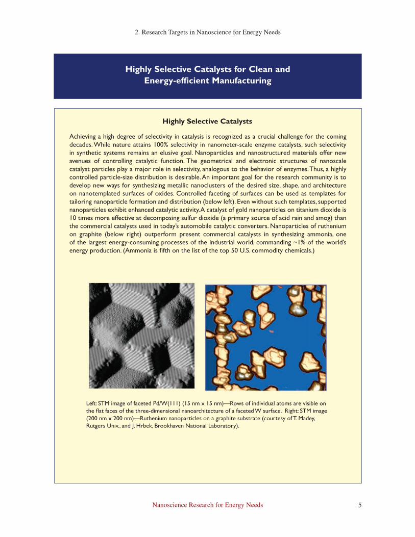
Achieving a high degree of selectivity in catalysis is recognized as a crucial challenge for the coming decades. While nature attains 100% selectivity in nanometer-scale enzyme catalysts, such selectivity in synthetic systems remains an elusive goal. Nanoparticles and nanostructured materials offer new avenues of controlling catalytic function. The geometrical and electronic structures of nanoscale catalyst particles play a major role in selectivity, analogous to the behavior of enzymes. Thus, a highly controlled particle-size distribution is desirable. An important goal for the research community is to develop new ways for synthesizing metallic nanoclusters of the desired size, shape, and architecture on nanotemplated surfaces of oxides. Controlled faceting of surfaces can be used as templates for tailoring nanoparticle formation and distribution (below left). Even without such templates, supported nanoparticles exhibit enhanced catalytic activity. A catalyst of gold nanoparticles on titanium dioxide is 10 times more effective at decomposing sulfur dioxide (a primary source of acid rain and smog) than the commercial catalysts used in today’s automobile catalytic converters. Nanoparticles of ruthenium on graphite (below right) outperform present commercial catalysts in synthesizing ammonia, one of the largest energy-consuming processes of the industrial world, commanding ~1% of the world’s energy production. (Ammonia is fi fth on the list of the top 50 U.S. commodity chemicals.)
Highly Selective Catalysts for Clean and Energy-effi cient Manufacturing
Left: STM image of faceted Pd/W(111) (15 nm x 15 nm)—Rows of individual atoms are visible on the fl at faces of the three-dimensional nanoarchitecture of a faceted W surface. Right: STM image (200 nm x 200 nm)—Ruthenium nanoparticles on a graphite substrate (courtesy of T. Madey, Rutgers Univ., and J. Hrbek, Brookhaven National Laboratory).

Nanoscience Research for Energy Needs6
2. Research Targets in Nanoscience for Energy Needs
Transmission electron micrographs of cadmium selenide nanocrystals used in a photovoltaic device. Tuning the size and aspect ratio of the nanocrystals gives control over the band gap and electron transport distance. External quantum effi ciencies of over 54% have been achieved (courtesy of A. P. Alivisatos, Univ. of California, Berkeley and Lawrence Berkeley National Laboratory).
Nanostructured Photovoltaics: Performance Goals and Opportunities
At the heart of all photovoltaic cells are two separate material layers, one with a reservoir of electrons that functions as the negative pole of the cell, and the other having vacancies of electrons, called electron holes, that functions as the positive pole. Absorption of light from the sun or another light source by the cell provides energy to drive the electrons from the negative to the positive pole, creating a voltage difference between them, thus enabling the cell to serve as a source of electrical energy. The low effi ciency of this conversion of light energy to electrical energy by conventional cells and their cost have prevented photovoltaic cells from being competitive with electrical energy generated from fossil fuels and nuclear power. For nanostructured photovoltaic devices to have a signifi cant impact on energy supply, the cell and module effi ciencies must have a lower cost/watt than the projected cost of conventional crystalline silicon photovoltaics. Nanotechnology has considerable potential to produce photovoltaic cells with signifi cant cost reduction, but must do so at cell effi ciencies greater than 14-15% and at costs < $100/m2 in order meet a cost goal of $1/W. Since module and balance-of-system costs are major components of the overall expense of photovoltaic systems, cells with effi ciencies below 10-12%—even if very inexpensive—will not realize these performance goals. Nanostructured photovoltaic devices must also be able to endure 15-30 years of outdoor operation with daily cycling to temperatures of 80–100oC at peak rates of solar radiation. Nanostructured devices such as quantum dots allow light to be collected from a broad range of wavelengths (colors) of the sun’s spectrum. These devices also gather more than one electron-hole pair per photon because they contain heterostructured absorber layers for broad spectral absorption (see diagram below). This structuring also enhances the effi ciency of low-quality materials to accumulate charge carriers or excitons. All have potential for breakthroughs in cost and performance in photovoltaics. Photovoltaics with effi ciencies at the level of this grand challenge will clearly make them economically competitive.
Harvesting of Solar Energy with 20% Power Effi ciency and 100 Times Lower Cost
Enhanced photovoltaic effi ciency in quantum dot solar cells by inverse Auger effect. (courtesy of V. Klimov, Los Alamos National Laboratory; reprinted by permission from Elsevier—see reference 33 on p. 63).

7Nanoscience Research for Energy Needs
2. Research Targets in Nanoscience for Energy Needs
Solid-state Lighting at 50% of the Present Power Consumption
Solid-State Lighting
At present, electricity use accounts for about one-third of total energy consumption in the United States. About 20% of all electricity consumed goes for lighting. However, today’s lighting is remarkably inefficient. Incandescent lights have a luminous efficiency of 15 lumens/watt and fluorescents have a luminous efficiency of 80 lumens/watt. This corresponds to converting only about 5% and 25%, respectively, of the electrical energy to visible light. By comparison, building heating is typically 70% efficient, and electrical motors are 85–95% efficient. Lighting therefore represents a large target for improving energy efficiency. Cutting the amount of electricity needed for lighting in half would result in a savings of 4 x10¹¹ kilowatt-hours of energy per year—roughly equivalent to the annual energy production of 50 nuclear reactors.
The use of semiconductor-based light emitting diodes (LEDs) for general illumination is a rapidly developing technology that offers the potential of immense energy savings to the nation and the world within a decade or two. For colored lighting, LEDs have already replaced over one-third of the traffic lights in the United States, resulting in a savings of about $1,000 per intersection per year. However, a number of science and technology obstacles must be overcome for solid-state lighting to reach its potential. The target now is to bring this new technology to the general white-lighting applications where the potential impacts are tremendous. To produce white light, one can have a source consisting of three or more different colored LEDs, or use ultraviolet light to illuminate phosphors that emit the different colors. The latter approach is far more economical, and much higher efficiencies have been demonstrated using semiconductor nanocrystals (quantum dots, QDs) as phosphors. Before these devices can be commercialized, improvement is required in the ability to incorporate quantum dots into the dome above the illuminating LED in a manner that retains their high efficiency.
Graph of U.S. Energy Consumption.
Efficiencies of Energy Technologies in Buildings:Heating: 70-80%Electric motors: 85-95%Fluorescent lighting: 25%Incandescent lighting: 5%
World’s first white-emitting LED using only QDs as phosphors. The LED chip is a 410 nm InGaN-based chip from Cree Research (courtesy of J. Simmons, Sandia National Laboratories).

Nanoscience Research for Energy Needs8
2. Research Targets in Nanoscience for Energy Needs
Super-Strong Lightweight Materials to Improve Efficiency of Cars, Airplanes, etc.
Ultra-High Strength, Lightweight Nanophase Materials
Nanoscale phases incorporated in bulk materials exhibit remarkable properties, such as enhanced magnetism, mechanical strength, and high-temperature tolerance, as well as being ultra-lightweight. This opens the opportunity to develop new classes of bulk materials that retain a nanograin size and display enhanced or new properties at the macroscale. Applications include structural components for high strength, magnets in motors and transformers, filters, and wires provide numerous examples of the benefits of nanoscale precipitates. For example, calculations predict that nanocomposite magnets made of Sm2Fe17Nd3 (samarium, iron, and neodynium) mixed with Fe65Co35 (iron and cobalt) will be 200% stronger than the best commercial magnets in use today. Applying these materials in motors and transformers will improve performance and lead to energy savings since smaller amounts of the stronger magnets are required resulting in lighter components. Replacing conventional distribution transformers with advanced nanostructured magnetic materials in the United States will result in and approximate annual savings of $3.5 billion and a 35 million ton reduction in CO2 emissions. Another example of enhanced functionality is the mechanically alloyed, oxide-dispersion strengthened (MA/ODS) iron (Fe)-12%, chromium (Cr)-3%, tungsten (W)- 0.4%, titanium (Ti) – 0.4 %, and 0.25% (yttrium) Y2O3 (12YWT) ferritic alloy. This new structural material possesses greater strength than steel and can perform at 150°C higher temperature. Key scientific barriers must be overcome to bring these materials to fruition. Improved synthesis and processing techniques must be developed to control nanoscale grains in these materials. The potential impact is a class of materials with longer life in aggressive environments (e.g., high temperatures or radiation), improved energy storage (batteries and fuel cells), functional materials for magnets (the use of bulk magnets is pervasive in small motors in transportation, and in large motors in electrical generators), and a host of new materials challenges in renewable energy.
Left: Transmission electron microscope image of the magnetic structure of nickel nanoparticles (courtesy of Y. Zhu, Brookhaven National Laboratory). Right: Atom probe reveals the presence of a very high number density of nano-size clusters in the 12YWT Alloy, providing structure and composition information (courtesy of D. T. Hoelzer, M. K. Miller, P. J. Maziasz, and C. L. Fong, Oak Ridge National Laboratory).
9Nanoscience Research for Energy Needs
2. Research Targets in Nanoscience for Energy Needs
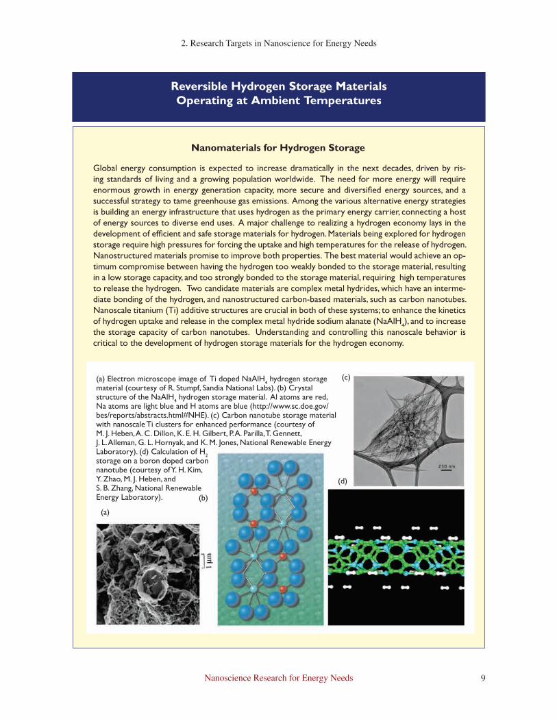
Nanomaterials for Hydrogen Storage
Global energy consumption is expected to increase dramatically in the next decades, driven by ris-ing standards of living and a growing population worldwide. The need for more energy will require enormous growth in energy generation capacity, more secure and diversified energy sources, and a successful strategy to tame greenhouse gas emissions. Among the various alternative energy strategies is building an energy infrastructure that uses hydrogen as the primary energy carrier, connecting a host of energy sources to diverse end uses. A major challenge to realizing a hydrogen economy lays in the development of efficient and safe storage materials for hydrogen. Materials being explored for hydrogen storage require high pressures for forcing the uptake and high temperatures for the release of hydrogen. Nanostructured materials promise to improve both properties. The best material would achieve an op-timum compromise between having the hydrogen too weakly bonded to the storage material, resulting in a low storage capacity, and too strongly bonded to the storage material, requiring high temperatures to release the hydrogen. Two candidate materials are complex metal hydrides, which have an interme-diate bonding of the hydrogen, and nanostructured carbon-based materials, such as carbon nanotubes. Nanoscale titanium (Ti) additive structures are crucial in both of these systems; to enhance the kinetics of hydrogen uptake and release in the complex metal hydride sodium alanate (NaAlH4), and to increase the storage capacity of carbon nanotubes. Understanding and controlling this nanoscale behavior is critical to the development of hydrogen storage materials for the hydrogen economy.
Reversible Hydrogen Storage Materials Operating at Ambient Temperatures
(a) Electron microscope image of Ti doped NaAlH4 hydrogen storage material (courtesy of R. Stumpf, Sandia National Labs). (b) Crystal structure of the NaAlH4 hydrogen storage material. Al atoms are red, Na atoms are light blue and H atoms are blue (http://www.sc.doe.gov/bes/reports/abstracts.html#NHE). (c) Carbon nanotube storage material with nanoscale Ti clusters for enhanced performance (courtesy of M. J. Heben, A. C. Dillon, K. E. H. Gilbert, P. A. Parilla, T. Gennett, J. L. Alleman, G. L. Hornyak, and K. M. Jones, National Renewable Energy Laboratory). (d) Calculation of H2 storage on a boron doped carbon nanotube (courtesy of Y. H. Kim, Y. Zhao, M. J. Heben, and S. B. Zhang, National Renewable Energy Laboratory).
(a)
(b)
(c)
(d)
Nanoscience Research for Energy Needs10
2. Research Targets in Nanoscience for Energy Needs
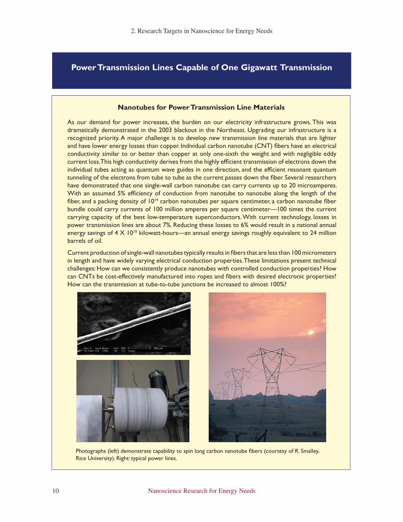
Power Transmission Lines Capable of One Gigawatt Transmission
Nanotubes for Power Transmission Line Materials
As our demand for power increases, the burden on our electricity infrastructure grows. This was dramatically demonstrated in the 2003 blackout in the Northeast. Upgrading our infrastructure is a recognized priority. A major challenge is to develop new transmission line materials that are lighter and have lower energy losses than copper. Individual carbon nanotube (CNT) fi bers have an electrical conductivity similar to or better than copper at only one-sixth the weight and with negligible eddy current loss. This high conductivity derives from the highly effi cient transmission of electrons down the individual tubes acting as quantum wave guides in one direction, and the effi cient resonant quantum tunneling of the electrons from tube to tube as the current passes down the fi ber. Several researchers have demonstrated that one single-wall carbon nanotube can carry currents up to 20 microamperes. With an assumed 5% effi ciency of conduction from nanotube to nanotube along the length of the fi ber, and a packing density of 1014 carbon nanotubes per square centimeter, a carbon nanotube fi ber bundle could carry currents of 100 million amperes per square centimeter—100 times the current carrying capacity of the best low-temperature superconductors. With current technology, losses in power transmission lines are about 7%. Reducing these losses to 6% would result in a national annual energy savings of 4 X 10¹⁰ kilowatt-hours—an annual energy savings roughly equivalent to 24 million barrels of oil.
Current production of single-wall nanotubes typically results in fi bers that are less than 100 micrometers in length and have widely varying electrical conduction properties. These limitations present technical challenges: How can we consistently produce nanotubes with controlled conduction properties? How can CNTs be cost-effectively manufactured into ropes and fi bers with desired electronic properties? How can the transmission at tube-to-tube junctions be increased to almost 100%?
Photographs (left) demonstrate capability to spin long carbon nanotube fi bers (courtesy of R. Smalley, Rice University). Right: typical power lines.

11Nanoscience Research for Energy Needs
2. Research Targets in Nanoscience for Energy Needs
Low-Cost Fuel Cells, Batteries, Thermoelectrics, and Ultra-Capacitors Built from Nanostructured Materials
Nanoparticles and Nanoarchitectures for Energy Conversion and Storage
Nanostructured materials offer a number of exciting opportunities for the development of enhanced power storage and conversion. Fuel cell catalysts fabricated with nanoparticles of ruthenium-platinum (Ru-Pt) outperform traditional catalysts in several important ways. They are much more resistant to carbon monoxide poisoning, operating 50 times longer than traditional fuel cell catalysts. Furthermore, the architecture of the nanocatalyst exposes all of the active platinum atoms on the ruthenium nanoparticles (below right), eliminating the need for much of the high-cost platinum, thus driving down the cost considerably and surpassing all DOE targets for low platinum loading.
Nanostructured architectures that employ a highly three-dimensional structuring for power storage (batteries, fuel cells, ultracapacitors, photovoltaics) provide many advantages over existing technologies to minimize power losses, improve charge/discharge rates, and enhance energy densities. Electrodes in these architectures will consist of interconnected ~10 nm domains and mesopores (10–50 nm). An ultrathin, conformal, and pinhole-free separator/electrolyte is electrodeposited onto the electrode nanoarchitecture. Low melting-point metals (mp < 200°C) or colloids fi ll the remaining mesoporous volume (below left). Controlling the morphology of the electrodes greatly improves charging and discharging rates and increases energy storage and power densities. New lithium batteries with nanostructure electrodes demonstrated over 2500 watts per kilogram power density, which is 10 times greater than conventional lithium batteries.
Nanoparticle (electrode)Oxide or carbon (electrode)
Polymer (separator/electrolyte)
CO tolerant fuel-cell catalyst
(Figures courtesy of M. S. Doescher, D. R. Rolison, J.W. Long, Naval Research Laboratory and R. Adzic, Brookhaven National Laboratory.)
~10 nm

Nanoscience Research for Energy Needs12
2. Research Targets in Nanoscience for Energy Needs
Nanoscience Imitates Life
The simplest living systems, bacteria and viruses, are micrometer-scale structures. The molecular machines inside them are nanometer-scale structures exhibiting a remarkable level of specificity and architectural control and seamless integration of functional components without parallel in human technology. In addition, living systems provide examples of functional mechanisms that can guide us in synthesizing new materials. These natural and bio-inspired systems perform remarkable functions, such as converting solar energy to chemical energy, selective catalysis, materials fabrication, and bioremediation. Coupling biological processes and functions to hard/inorganic components leads to exciting possibilities in harnessing solar energy to produce electricity or fuels such as hydrogen, and in developing chemical processes with low environmental impact. Two examples are shown below. The figure on the left shows that a new device for solar energy harvesting and conversion can be assembled by coupling proteins with solid-state materials. The figure on the right shows a nanoscale artificial reaction center that has been synthesized to convert light energy into electrochemical potential, mimicking nature.
Achieving feedback from and control of biological systems is being approached both by the design of non-natural components that imitate biological systems and by their selective combinations with natural components. The challenge is to adapt and use these components for purposes beyond what nature had intended. The energy applications of biologically inspired nanosystems are likely to occur in the form of low-impact energy harvesting, which can be coupled to power nanoscale devices, selective catalysis, or materials synthesis.
Materials Synthesis and Energy Harvesting Based on the Efficient and Selective Mechanisms of Biology
Above: Photosynthetic reaction center coupled to solid-state structure leading to functional nanoscale device for solar energy harvesting. Right: Artificial photosynthetic reaction center (courtesy of M. A. Firestone, Argonne National Laboratory and D. Gust, Arizona State University).

13
3. Crosscutting Themes
Nanoscience Research for Energy Needs
CATALYSIS BY NANOSCALE MATERIALS
Vision
Catalysis controls the rates at which chemical bonds are formed and broken, thereby controlling the yields of desired products over undesired ones in chemical reactions. Catalysis is therefore central to energy conversion and environmental protection—as well as to a healthy economy. Catalysts are vital for the conversion of petroleum and other fossil fuels, the cleaner emissions of modern cars and fossil-fuel power plants. The petroleum, chemical, and pharmaceutical industries that rely on catalysts contribute $500 billion annually to the gross national product of the United States.
Today, we face new challenges in creating alternative fuels, cleaning the environment, dealing with the causes of global warming, and keeping us safe from toxic substances and infectious agents. Catalysis can help us meet these challenges, but the complexity and diversity of catalysts demand a revolution in the way they are designed and used. This revolution can become reality by the application of new materials and methods emerging from nanoscience.
The opportunities to understand and predict how catalysts work at a fundamental level have unfolded dramatically in the past 20 years with the emergence of powerful predictive methods such as density functional theory, incisive instruments for imaging at the nanoscale, and dedicated facilities for examining catalysts as they function, even at the high temperatures and pressures used in industrial processes. New approaches, such as rapid-throughput catalyst testing methods and terascale computational methodologies, coupled with the emergence of nanoscience and the research facilities to support it, increasingly place catalysis science on the threshold of new understanding and new technology for energy conversion.
The research challenge in nanoscience for catalysis is learning to tune the energy landscape of the chemical reactants as they interact with nanostructured catalytic materials. Drawing from the lessons of biology, we must design nanostructured materials to match the structural conformation of the reactant and to control the reaction pathway to the desired product. To accomplish this, new and efficient methods of in situ characterization and rapid throughput testing of catalytic properties will be required. The choice of materials, structural parameters, and experimental design must be guided by continually improving our fundamental understanding of the structure-function relationships of nanostructured catalysts.
Background/State of the Art
For the foreseeable future, the major source of energy for the nation will be found in chemical bonds. Accessing and using this energy source will rely on our developing efficient, selective, and economical catalysts. Nanomaterials offer a new paradigm for the development of catalysts. Materials that in the bulk form have little or no catalytic activity can exhibit exceptional catalytic behavior in nanoscale form. The best example is the system of gold nanoparticles supported on a titanium dioxide substrate. Gold in its bulk form is known for its inert properties, making it useful in corrosion-resistant coatings and art and dental fillings. However, Haruta and coworkers [1] discovered that nanoparticles of gold in the five nm regime dispersed on a titania substrate are remarkably active for important reactions such as
3. Crosscutting Themes

Nanoscience Research for Energy Needs14
3. Crosscutting Themes
hydrocarbon epoxidation and CO oxidation at low temperatures (Fig. 3.1). This initial work has spurred further investigations into the importance of the gold nanoparticle size and the role of the substrate support.
However, these materials are typically discovered by Edisonian methods and have complex, nonuniform, and poorly understood nanostructures. If scientists and engineers could precisely design the structures of such materials, they could control the relationship between catalyst structure and catalytic chemistry. The effects on energy production and use in both domestic and industrial applications would be profound. Nanoscience provides the opportunity for this precise design. Nature’s catalysts, enzymes, show how amazingly effi cient catalysts can be—they make possible essentially all biological reactions—and, by comparison with today’s technology, they show how much opportunity there is for improvement. Control and effi ciency of chemical conversion comparable to that demonstrated by nature are in sight for countless known and unknown reactions, as we learn how catalysts work and how to engineer them for specifi c reactions. We are faced with a grand challenge of designing completely new catalysts and catalytic processes for as yet unimagined purposes and benefi ts. The emerging tools of nanoscience will be central to meeting this challenge. With these tools, we can envision such technologies as one-step conversion of cellulose or CO
2 into liquid fuels, economical photocatalytic conversion of water into
hydrogen (and oxygen) for a hydrogen economy, and effi cient fuel cells for the conversion of hydrogen to power automobiles and heat homes.
Major Technical Challenges
Most catalysts need to operate at high temperature and pressure, so nanomaterials that are stable under these conditions are required. The catalysts also must be stably dispersed—i.e., present on solid supports, where they are accessible to reactant molecules. The supports provide high surface area per unit volume and are, therefore, porous materials, usually at the nanoscale. Catalysts are usually present on the surfaces of these supports or partially embedded in them. Thus, catalysts are typically nanoparticles within nanoporous materials, and the connections between them are interfaces that are referred to as hidden because they are not susceptible to imaging as is an extended fl at surface.
Catalyst performance is determined by the composition, size, morphology, and degree of uniformity of the nanoparticles, the support, and the interface between them. Thus, to understand catalysts and develop
Figure 3.1. Transmission electron micrograph of gold (Au) nanoparticle catalysts on a titania (TiO2) support.
The remarkable catalytic behavior of the gold nanoparticles for CO oxidation is shown on the right as a function of their size (© 1997 Elsevier; reprinted by permission [1]).
Nanoscience Research for Energy Needs 15
3. Crosscutting Themes
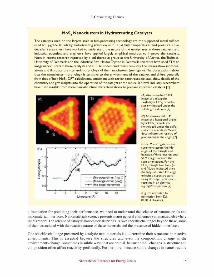
(A) Atom-resolved STM image of a triangular single-layer MoS2 nanoclu-ster synthesized under the sulfi ding conditions [2].
(B) Atom-resolved STM image of a hexagonal single-layer MoS2 nanocluster synthesized under the sulfo-reductive conditions. White dots indicate the registry of protrusions at the edges [2].
(C) STM corrugation mea-surements across the Mo edges of the triangle and hexagon. White lines on both STM images indicate the scan orientations. For the MoS2 triangle two lines, (i) and (ii), are indicated since the fully saturated Mo edge exhibits a superstructure along the edge protrusions, resulting in an alternat-ing high/low pattern [2].
(Figures reprinted by permission from [2]. © 2004 Elsevier.)
MoS2 Nanoclusters in Hydrotreating Catalysts
The catalysts used on the largest scale in fuel-processing technology are the supported metal sulfi des used to upgrade liquids by hydrotreating (reaction with H2 at high temperatures and pressures). For decades, researchers have worked to understand the nature of the nanophases in these catalysts, and industrial scientists and engineers have applied largely empirical methods to improve the catalysts. Now, in recent research reported by a collaborative group at the University of Aarhus, the Technical University of Denmark, and the industrial fi rm Haldor Topsøe in Denmark, scientists have used STM to image nanoclusters in these catalysts and DFT to understand their chemistry. The images show individual atoms and illustrate the size and morphology of the nanoclusters (see fi gure). The observations show that the nanocluster morphology is sensitive to the environment of the catalyst and differs generally from that of bulk MoS2. DFT calculations, consistent with earlier spectroscopic data, show details of the chemistry and give insights into the operation of the catalyst at the molecular level. Industry researchers have used insights from these nanostructure characterizations to prepare improved catalysts [2].
a foundation for predicting their performance, we need to understand the science of nanomaterials and nanomaterial interfaces. Nanomaterials science presents major general challenges summarized elsewhere in this report. The science of catalytic nanomaterials brings its own specifi c challenges beyond these, some of them associated with the reactive nature of these materials and the presence of hidden interfaces.
One specifi c challenge presented by catalytic nanomaterials is to determine their structures in reactive environments. This is essential because the structures and even the compositions change as the environments change, sometimes in subtle ways that are crucial, because small changes in structure and composition often affect reactivity profoundly. Furthermore, because subtle changes in nanostructure

Nanoscience Research for Energy Needs16
3. Crosscutting Themes
and composition can have such great consequences on a catalyst’s performance, we must develop rapid, effi cient methods for testing the performance of many candidates en route to fi nding the best catalyst for an application.
Fuel Cell Catalysts
Recent workshops and reviews of the status of fuel-cell technology all conclude that new materials for every component of fuel cells are essential to the widespread introduction of this technology [3-6]. These are sorely needed to considerably improve performance (e.g., faster kinetics, less sensitivity to poisons, etc.) and reliability (durability), as well as to lower cost. Improved electrocatalysts are vital for anodes and cathodes, and for improved ionically conducting membranes in low-temperature fuel cells (below approx. 150oC). More specifi cally, as new, more complex catalyst materials are explored, we must fi nd effi cient, generally applicable routes to the formation of nanoparticles with diameters from three to fi ve nm so that the materials can be routinely and rapidly evaluated in realistic fuel-cell confi gurations and designs.
Improved Nanoparticle Platinum-Based Catalysts
An example of state-of-the-art synthesis in an energy-related area involves synthesis of a nanocatalyst for hydrogen oxidation in fuel cells. Using techniques from electrochemistry, researchers at Brookhaven National Laboratory synthesized ruthenium nanoparticles with a sub-monolayer of platinum atoms on the surface as catalysts for hydrogen oxidation in fuel cells for the hydrogen economy. This is attractive for catalytic applications due to the potentially low platinum loading of this catalyst, because every platinum atom is on the surface, as shown in Fig. 3.2. The synthesis techniques allow for careful control of the nanocatalyst and for production of quantities for fuel cell testing.
The impact of this nanocatalyst in fuel cells is illustrated in the right panel of Fig. 3.2. This shows the current as a function of time when the fuel cell is exposed to a very high concentration of CO. The blue and green curves show the decay of current that results from CO poisoning in commercial catalysts. The red curve shows that the nanocatalyst demonstrates a signifi cantly enhanced tolerance to CO poisoning compared to the commercial catalysts. This enhanced CO poisoning tolerance in combination with the low platinum loading makes this type of hybrid nanocatalyst of great interest.low platinum loading makes this type of hybrid nanocatalyst of great interest.
Figure 3.2. Left: Ruthenium nanoparticles with adsorbed platinum atoms, a nanocatalyst for hydrogen reduction. Right: Performance of this nanomaterial (red line) for tolerance to CO poisoning in fuel-cell operation showing greater performance compared to commercial catalysts (green and blue) (courtesy of R. Adzic, Brookhaven National Laboratory [7]).

Nanoscience Research for Energy Needs 17
3. Crosscutting Themes
Challenge for Catalyst Selectivity
A major challenge for nanocatalysts is the development of catalysts with performance characteristics rivaling those of enzymes. These catalysts are responsible for steering almost all reactions in living organisms. They are extremely complex in structure and subtle in function. Working in dilute aqueous solutions in the presence of mixtures of many kinds of reactive molecules at ambient temperatures, enzymes are highly active and 100% selective, and, through biosynthesis, they are replaced as needed in living organisms. Synthetic catalysts with properties approaching those of enzymes would truly revolutionize the technology of energy conversion. For example, one would envision waste-free or “green chemistry” in converting biomass into fuels. To this end, nature can provide tremendous guidance and insight, and the future of catalysis by nanomaterials is sure to derive countless inspirations from biology.
Infrastructure Needs
Meeting the ultimate challenge of predicting new catalysts for new conversions will require major developments in our science infrastructure.
Fundamental understanding of nanomaterials in reactive environments will require novel methods and facilities to elucidate the compositions, structures, and morphologies of nanoparticles, nanoporous
Degree of Disorder / # of Li stored.
As Li+ and e- are inserted, does the V formal oxidation state truly
track as V5+=>V4+=>V3+=>V2+?
The Importance of Disorder
Improved performance in energy storage and conversion has been demonstrated using highly defective nanoscale inorganic materials in battery chemistry (e.g., Li-ion insertion into V2O5 aerogels at unprecedented Li-to-V stoichiometries, see below) and electrocatalyzed fuel-cell reactions. Nanoscale Pt-RuOxHy is 250 times more active for direct oxidation of methanol than is nanoscale Pt50Ru50 alloy. Improvements of this magnitude require characterizing the nature of these high performance, but not highly crystalline or ordered materials.
Most of the standard materials science characterization tools provide high-quality information on bulk, periodic, or crystalline materials; equally high-quality characterization is needed for functionally relevant disorder, especially on the nanoscale. We then need to fi nd physiochemical means to stabilize functionally relevant disorder in nanomaterials and nanoarchitectures in the face of electric fi elds, magnetic fi elds, electron-volts of photonic energy, temperature, pressure, and/or chemical potential when in use in energy storage and conversion devices. One future path of nanoscale design and synthesis of disordered high-performance energy materials may be to mimic glass science; however, to stabilize a technically important but unstable glass composition, another ingredient may be necessary. Computational chemistry will be key in selecting stabilizing components [8-9].
(Figure reprinted by permission from [9], courtesy of The Electro-chemical Society, Inc.)

Nanoscience Research for Energy Needs18
3. Crosscutting Themes
materials, and their combinations, including the interfaces. Specifically, it is essential to image these materials at the atomic scale, to measure spectra of various kinds, and to apply computation and theory, all under the same conditions. This major challenge will require new methods for nanomaterials synthesis, new and improved instruments and facilities, and extensive collaborations between experimentalists and theorists. We must develop methods to measure catalyst performance simultaneously with measurements of images and spectra, all with speed and high efficiency. Advances are needed for imaging three-dimensional materials and interfaces, and spectroscopic methods must be adapted to nanoscales. Important directions to follow include the effective use of the emerging capabilities for imaging by high-resolution transmission electron microscopy (TEM) and scanning probe microscopy (SPM), spectroscopic characterization at light sources and neutron sources as well as improvements in dedicated laboratory equipment, and theoretical representation by advanced computation. This will require key improvements in the facilities, as well as advancement of sample handling methods and instrumentation to ensure investigation of the same samples under the same conditions by these complementary techniques. Techniques are needed to allow imaging with simultaneous spatial and temporal resolution of changes in catalyst nanostructures as the catalysts operate, so as to demonstrate concurrently how the performance of the catalyst is linked to the images and spectra as they are recorded.
Advances in nanoscience, facilitated by applications of computation and theory in concert with experiment, will facilitate rapid progress in catalysis. The science will benefit greatly from the emerging ability to make uniform catalysts that can be understood fundamentally, without the complications of non-uniform materials that have a range of catalytic properties. The emerging ability to image, manipulate, and spectroscopically interrogate single catalytic nanoparticles will complement the research with uniform nanoparticles. Investigations of arrays of nanoparticles will facilitate understanding of the effects of nanoarchitecture, including interactions of nanoparticles and transport of reactants and products in catalytic materials. Advances in femtosecond science will allow us to time-resolve structural changes on ultrafast timescales, thus adding new dimensions to understanding primary chemical reactions. Theory can now provide reliable calculations of thermodynamics and dynamics for model catalytic reactions. Combinatorial synthesis and rapid screening methodologies are already providing leads to new catalysts at an unprecedented rate, and the integration of these methods with imaging and spectroscopy of functioning catalysts will propel the field forward. New, powerful techniques, such as scanning tunneling microscopy, synchrotron and neutron sources, terascale computational methodologies, and especially the new nanoscience research centers, will all place catalysis science on the threshold of new understanding and new technology. Developments in structural biology are already providing insights into the workings of catalysts, leading to the anticipation that bioinspired catalysts of the future will provide rapid, selective conversions of dilute reactants under mild conditions, even in aqueous environments.
What Can Emerge from Research on the Nanoscience of Catalysis?
We can envision new catalysts that will allow economical one-step conversion of methane into methanol or other liquid fuels. Similarly, cellulosic raw materials or CO
2 might be converted into liquid fuels.
Improved fuel cell catalysts may lead the way to economical fuel cells for the conversion of H2 or
methanol or even gasoline. Improved catalysts may allow small, lightweight devices in automobiles for on-board conversion of liquid fuels into H
2 for fuel cells, eliminating the need for hydrogen storage.
Nanoscience Research for Energy Needs 19
3. Crosscutting Themes
USING INTERFACES TO MANIPULATE ENERGY CARRIERS
Vision
The use of engineered nanostructures at interfaces has demonstrated a compelling potential for improving energy security based on advances in efficient power handling, low-power electronics, energy harvesting, and efficient energy use in lighting. The most significant research challenge impeding these advances is the need to create interfaces that are tailored at the nanoscale to optimize transport of energy in many forms (electrons, phonons, photons, excitons). The issues related to the transport of each form of energy are discussed separately below; the crosscutting research challenge of tailoring the interface response is apparent in all four cases.
Electron Transport
Electron transport is an old problem of ubiquitous significance. Both transport of electricity along conducting lines and use of electricity in appliances and information processing is subject to energy loss—the result is energy wasted in creating unwanted heat. One of the most exciting successes of nanoscience has been the demonstration of lossless electron conduction, or quantized conduction. This is illustrated in the box below, where the potential of vastly increasing efficiency of energy transmission through the novel properties of carbon nanotubes is presented. This illustration also raises one of the continuing challenges of nanoscience, which is developing controlled-electron transport across nanoscale interfaces—in this case the nanotube-nanotube interface.
Transport of electrons across material interfaces is determined by the quantum-mechanically defined electron energies at each side of the interface, and any chemical reactions and energy barriers between the two sides of the interface, as illustrated in the line drawings of Fig. 3.3. The nature of electronic transport
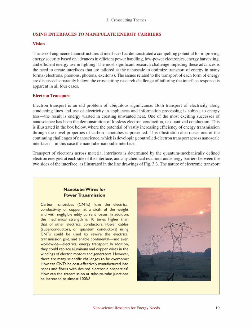
Nanotube Wires for Power Transmission
Carbon nanotubes (CNTs) have the electrical conductivity of copper at a sixth of the weight and with negligible eddy current losses. In addition, the mechanical strength is 10 times higher than that of other electrical conductors. Power cables (superconductors, or quantum conductors) using CNTs could be used to rewire the electrical transmission grid, and enable continental—and even worldwide—electrical energy transport. In addition, they could replace aluminum and copper wires in the windings of electric motors and generators. However, there are many scientific challenges to be overcome: How can CNTs be cost-effectively manufactured into ropes and fibers with desired electronic properties? How can the transmission at tube-to-tube junctions be increased to almost 100%?

Nanoscience Research for Energy Needs20
3. Crosscutting Themes
across such barriers is a classical problem in electronics and has been evaluated extensively, generally in the context of flat two dimensional interfaces. The new issues that arise in nanoscience are (a) the exploration and use of a broad spectrum of non-traditional materials, which introduce a multidimensional parameter space of possible interface chemistry/electronic structure; and (b) the complex electric fields that result from the three-dimensional nanoscale structure of interfaces involving nanoparticles and nanodevices. Both of these effects are illustrated in the sidebar on the following page.
Exploring the full range of chemistry, atomic structure, and three-dimensional configuration that can arise in fabricating nanoscale interfaces introduces a combinatorially large parameter space. The key issues in nanoscience discussed in other sections of this report are imperative here as well:
1. Intelligent design of experiments based on theory and modeling to predict productive arenas of investigation
2. Optimizing materials and chemistry choices, and developing growth and assembly techniques
3. In situ characterization in which structure/property relationships can be established directly
The choice of materials and optimizing the synthesis/growth/assembly conditions remain critical and creative parts of the nanoscience endeavor. Materials may be thin films or membranes and may be patterned via lithographic techniques, imprint techniques, templated self-assembly, and/or controlled reactions. Alternatively, materials may be nanoparticles that may be assembled electrostatically, via chemical linkages, or via nucleated growth. Interfaces between different combinations of materials may be modulated by control of the structure and chemistry at the interface. The development of nanomaterials systems is coupled with constant evaluation of the desired properties, in this case interfacial transport. Fabricating nanostructures into device configurations (using both lithographic approaches and self-assembly approaches) is a powerful method for assessing the properties of interfacial transport. These
Figure 3.3. Illustration of some energy issues in electron transport across an interface between a metal and film of organic material. Electron transfer can only occur from a filled energy state and into a (quantum mechanically defined) empty state of appropriate energy. The offset of the energy levels on either side of the interface can modify the transport properties at the interface by introducing an electric field (dipole) at the interface, as illustrated at the left. When there are mobile carriers, charge transport to or from the interface occurs, creating band bending, which can produce an accumulation of free carriers at the interface. When there is a barrier, electrons (or holes) move across the interface via tunneling through or hopping over the barrier. The width of the barrier decreases with the strength of the chemical interaction across the interface, generally increasing the transmission rate (courtesy of V. Ballarotto, Laboratory for Physical Science, MD. See also Ref. [10]).

Nanoscience Research for Energy Needs 21
3. Crosscutting Themes
Nanoelectronics Illustrates Transport at Nanoscale Interfaces
Top down (lithographic) integration of a carbon nano-tube into an FET configuration, shown above, reveals that the complex electric fields around the nanoscale struc-ture offer new opportunities for controlling electron flow across the source and drain interfaces. Changes in transport via direct chemical modification of the inter-facial can be diagnosed in such a configuration as shown in the figure to the left (courtesy of P. Avouris, IBM).
properties must be understood to enable progress in thermoelectrics, photovoltaics, and lighting, as well as in nanoelectronics. Direct characterization of the transport properties must be coupled with careful measurements of structure and electromagnetic properties at the interface.
The state-of-the-art tools for directly assessing electrical properties at the nanoscale interface are often based on scanned probe techniques or highly focused probe beams (light, electrons) (Fig. 3.4). These techniques include the use of magnetic force microscopy [11] and scanning hall probe [12] to
Field-effect transistors based on carbon nanotubes are the prototype of the flexible nano-electronic systems envisioned for the future. As shown in the schematic (right), the conventional semiconductor conduction channel between the source and drain is formed here by a carbon nanotube (CNT). Conduction through the CNT is controlled by changing the voltage applied at the gate. Low power use and the ability to integrate sensors and feedback into control systems that optimize energy use are important energy drivers.
In addition to direct applications in nanoelectronics, fabricating nanostructures into device configurations serves as a major tool for characterizing electron transport across nanoscale interfaces (courtesy of P. Avouris, IBM, T.J. Watson Research Laboratory).
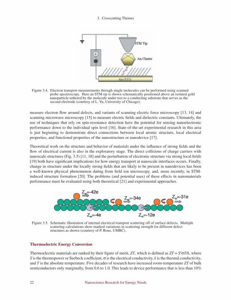
Nanoscience Research for Energy Needs22
3. Crosscutting Themes
Figure 3.4. Electron transport measurements through single molecules can be performed using scanned probe spectroscopy. Here an STM tip is shown schematically positioned above an isolated gold nanoparticle tethered by the molecule under test to a conducting substrate that serves as the second electrode (courtesy of L. Yu, University of Chicago).
Figure 3.5. Schematic illustration of internal electrical transport scattering off of surface defects. Multiple scattering calculations show marked variations in scattering strength for different defect structures as shown (courtesy of P. Rous, UMBC).
measure electron flow around defects, and variants of scanning electric force microscopy [13, 14] and scanning microwave microscopy [15] to measure electric fields and dielectric constants. Ultimately, the use of techniques that rely on spin-resonance detection have the potential for sensing nanoelectronic performance down to the individual spin level [16]. State-of-the-art experimental research in this area is just beginning to demonstrate direct connections between local atomic structure, local electrical properties, and functional properties of the nanostructure or nanodevice [17].
Theoretical work on the structure and behavior of materials under the influence of strong fields and the flow of electrical current is also in the exploratory stage. The direct collisions of charge carriers with nanoscale structures (Fig. 3.5) [11, 18] and the perturbation of electronic structure via strong local fields [19] both have significant implications for how energy transport at nanoscale interfaces occurs. Finally, change in structure under the locally strong fields that are likely to be present in nanodevices has been a well-known physical phenomenon dating from field ion microscopy, and, more recently, in STM-induced structure formation [20]. The problems (and potential uses) of these effects in nanomaterials performance must be evaluated using both theoretical [21] and experimental approaches.
Thermoelectric Energy Conversion
Thermoelectric materials are ranked by their figure of merit, ZT, which is defined as ZT = S2σT/k, where S is the thermopower or Seebeck coefficient, σ is the electrical conductivity, k is the thermal conductivity, and T is the absolute temperature. Five decades of research have increased room-temperature ZT of bulk semiconductors only marginally, from 0.6 to 1.0. This leads to device performance that is less than 10%

Nanoscience Research for Energy Needs 23
3. Crosscutting Themes
Solid-State Thermoelectric Energy Conversion
Solid-state thermoelectric engines and refrigerators contain no moving parts and can directly convert energy between heat and electricity. Furthermore, unlike conventional internal combustion engines or fuel cells, thermoelectric engines are not fuel specific, i.e., one can use any fuel as an energy source, including environmentally friendly ones. So why aren’t thermoelectric engines and refrigerators widely used in our everyday life? The issue is that of efficiency: today’s thermoelectric devices have about one-fourth the efficiency of conventional engines and refrigerators. Five decades of research have led to marginal improvement in performance, making the search for high-performance thermoelectric materials one of the biggest challenges in materials science. Over the past three years, however, multiple materials have been discovered that have led to dramatic increases in performance [24]. In all these cases, researchers have found the materials to be nanostructured. The difference comes from the presence of interfaces that selectively allow electrons to flow across them, but block heat flow by lattice vibrations or phonons. Nanostructuring allows one to dramatically increase the density of interfaces, which could improve the device performance to more than three times that of conventional bulk materials. These recent discoveries have given scientists hope that it may finally be possible to develop nanostructured thermoelectric materials and devices whose efficiencies are comparable to conventional engines and refrigerators.
Thermoelectric devices directly convert energy from heat to electricity. Nanostructured thermo-electric materials with multiple interfaces achieve this by allowing electrons to flow but blocking phonons that conduct heat. This could increase efficiency to more than three times that of con-ventional bulk materials (courtesy of A. Majumdar, UC Berkeley and Lawrence Berkeley Laboratory).

Nanoscience Research for Energy Needs24
3. Crosscutting Themes
of the Carnot limit. For the performance to reach 30% of the Carnot limit and, thereby, be comparable to their macroscopic gas or vapor-based counterparts, one must develop materials with ZT > 3. The challenge lies in the fact that S, σ, and k are interdependent—changing one alters the others, making optimization extremely difficult. The only way to reduce k without affecting S and σ in bulk materials is to use semiconductors of high atomic weight, such as Bi
2Te
3 and its alloys with Sb, Sn, and Pb. High
atomic weight reduces the speed of sound in the material, and thereby decreases the thermal conductivity. Although in principle there is no limit to increasing ZT, there are no candidate bulk materials in the horizon with ZT > 3 [22, 23]. Clearly, this has been one of the grand challenges of materials science, with major implications for energy [24].
Over the last three years, however, there have been reports of dramatic increases in ZT [25-27]. In all these cases, the material has been found to be nanostructured. This has obviously raised the question of whether quantum effects play any role, since they have been shown to increase ZT [28, 29]. What is the underlying science? In semiconductors, electrons and holes carry charge, while lattice vibrations or phonons dominate heat transport. Electrons/holes and phonons have two length scales associated with their transport—wavelength, λ, and mean free path, l. By nanostructuring semiconductors with sizes comparable to λ sharp edges and peaks in their electronic density of states are produced whose location in energy space depends on size. By matching the peak locations and shape with respect to the Fermi energy, one can tailor the thermopower. Furthermore, such quantum confinement also increases electronic mobility, which could lead to high values of σ. Hence, quantum confinement allows manipulation of S2σ that is difficult to achieve in bulk materials.
It is entirely possible, though, that the increase of ZT may be less dependent on quantum confinement of electrons and holes and more on phonon dynamics and transport. For example, if the size of a semiconductor is smaller than the mean free path of phonons and larger than that of electrons/holes, one can reduce thermal conductivity by boundary scattering without affecting electrical transport. While charge transport in thermoelectricity is almost monochromatic (energy levels within a few kT around the Fermi energy), heat transport by phonons is broadband over the Brillouin zone. Many bulk thermoelectric materials are alloys because alloy scattering of the short wavelength acoustic phonons suppresses thermal conductivity without significantly altering S2σ. However, the mid-long wavelength phonons remain unaffected and conduct heat in alloys. Can one beat the alloy limit? It is possible that embedded nanostructures in semiconductor alloys could scatter the mid-long wavelength phonons as well, due to the similarity in sizes, and thereby reduce the thermal conductivity below the alloy limit [30, 31]. However, the efficiency of scattering depends on the mismatch in acoustic impedance between the two materials.
Given all these possibilities, it is unclear which effect can be exploited most readily to increase ZT. What is clear, though, is that if one has to increase ZT beyond 3, it is imperative that we understand how charge and heat transport occur in semiconductor nanostructures, especially across interfaces. These recent discoveries have given scientists hope that it may finally be possible to develop nanostructured thermoelectric materials and devices whose efficiencies are comparable to conventional engines and refrigerators. However, there are many scientific and engineering challenges to be overcome: How do we design interfaces that selectively transmit electrons and holes, while blocking phonons across the whole Brillouin zone? How can we manufacture bulk quantities of nanostructured thermoelectric materials that have long-term stability at operating temperatures? How can we develop the theoretical and experimental tools required to understand the fundamental science of charge and heatflow at the relevant length and time scales? Answers to these questions could lead to high-performance thermoelectric devices that have the potential to dramatically change the way energy is converted directly between heat and electricity in the future.

Nanoscience Research for Energy Needs 25
3. Crosscutting Themes
Nanostructured Photovoltaics
In the long term, solar energy is the only source of renewable energy that has the capacity to fill humanity’s technological needs. Major improvements in the conversion efficiency, cost, and stability of solar devices are needed for the increased application of solar energy to be practical (Fig. 3.6). As indicated in a recent report of the Department of Energy’s Basic Energy Sciences Advisory Committee [3], “The grand challenge for solar energy utilization is to develop conversion systems that are stable and robust for a 20-30 year period and that result in a 10- to 50-fold decrease in the cost-to-efficiency ratio for the production of electricity and fuels.” While cells based on single-crystal silicon have advanced markedly over the years in terms of increased performance and lower cost, it is doubtful that such cells will be sufficiently inexpensive to compete with electricity and hydrogen derived from fossil fuels.
Figure 3.6. Efficiency of photovoltaic devices (© 1999 AAAS; reprinted by permission [32]).
Nanotechnology has considerable potential to realize cost reduction of photovoltaic cells, but must do so at cell efficiencies greater than 14-15% and at costs less than $100/m2 in order meet a cost goal of $1/W. Nanostructured photovoltaic devices must also be able to endure 15-30 years of outdoor operation with daily cycling to temperatures of 80-100oC at peak insolation. Recent work has demonstrated that thin film cells based on nanoparticulate materials can be fabricated and show reasonable efficiencies and stabilities. For example, the photovoltaic cell based on dye-sensitized nanoparticles of TiO
2 (dye-
sensitized solar cell, also known as the Grätzel cell) has been the subject of intense study for several years and can be fabricated in an inexpensive flexible plastic format. The operation of the cell (Fig. 3.7) is based on photogeneration of electron-hole pairs in the dye, with the electron rapidly moving into the TiO
2
and the hole being filled by a suitable electron donor (e.g., liquid phase electrolyte containing iodide). Problems remain in terms of improving the efficiency and stability. The challenge is also to eliminate the liquid phase and to discover alternative electron donors, preferably based on solid-state materials.
The liquid phase can be eliminated by making heterojunction polymer devices that contain blends of conjugated polymers (e.g., MEH-PPV) with a nanostructured inorganic material (see band diagram). Photon absorption creates excitons in the polymer, which diffuse about 20 nm before recombining. Hence, to achieve reasonable efficiencies, the electron-capturing inorganic electrode must be placed

Nanoscience Research for Energy Needs26
3. Crosscutting Themes
within the exciton diffusion lengths. The challenge is to cost-effectively manufacture such composites on a large scale with precision down to 10–20 nm. In addition, hole mobilities in the organic phase must be increased to improve efficiency. This requires fundamental research in charge transport in polymers.
Nanostructured materials, such as quantum dots and wells, enable the collection of more than one electron-hole pair per photon. These nanostructures contain absorber layers for broad spectral absorption and collect charge carriers or excitons with enhanced efficiency in low-quality materials. They all have potential for cost and performance breakthroughs in photovoltaics [33, 34] (Fig. 3.8). The challenge again is to cost-effectively manufacture quantum structures on a large scale.
Figure 3.7. Grätzel cell.
Figure 3.8. Enhanced photovoltaic efficiency in quantum dot solar cells by inverse Auger effect—impact ionization (courtesy V. Klimov, Los Alamos National Laboratory; reprinted by permission from Elsevier [33]).
Finally, biology has developed effective and durable nanoscale technologies for solar conversion through over a billion years of evolution. The process of photon-electron energy conversion in molecules is essentially a nanoscale process, which must be integrated with inorganic nanostructured materials for photovoltaics. It makes eminent sense to uncover the basic chemical and physical principles of photosynthesis and apply them to the development of nanoscale technologies for solar conversion.
Conduction band
Valence band
PolymerAl
Energy (eV) w.r.t vacuum level
-3
-4
-5
-6
LUMO
HOMO
Inorganic
ITO

Nanoscience Research for Energy Needs 27
3. Crosscutting Themes
Photosynthetic Reaction Centers: Understanding and Controlling the Molecule-Materials Interface
Natural photosynthetic reaction centers are nanoscale photovoltaic devices that convert light energy into electrochemical potential energy. Artificial reaction centers, such as the one shown in the figure below, perform a similar function. Porphyrin molecules collect light energy and use it to transfer an electron to a fullerene, generating an energy-storing charge-separated state with high quantum yield. But there are two major obstacles to using natural or artificial photosynthetic structures to produce useful electrical energy. First, the miniscule photovoltaics must be arranged into nanoscale architectures that promote electron transport and prevent energy-wasting recombination. Second, the molecular or biological materials must be interfaced with conducting materials to harvest the electrical energy. Learning to design suitable nanoscale organizational structures and interfaces is a major experimental and theoretical challenge (courtesy of D. Gust, © Arizona State University; reprinted by permission).
Lighting
The use of semiconductor-based light emitters (composed either of inorganic—LEDs—or organic materials—OLEDs) for general illumination is a rapidly developing technology that offers the potential of immense energy savings to the nation and the world within a decade or two. However, a number of science and technology obstacles must be overcome in order for solid-state lighting to reach its potential. The majority of these obstacles involve understanding electron-hole recombination at nanoscale interfaces. LEDs and OLEDs each have their own potential markets.
Nanoscience Research for Energy Needs28
3. Crosscutting Themes
OLEDs
It is anticipated that OLEDs will serve as large-area, flexible, lightweight sources that will create new lighting opportunities, as discussed in the recent Optoelectronic Industry Development Association 2002 OLED roadmap [35]. The materials employed in OLEDs are thin films of polymers or small molecules that efficiently transport injected charge (Fig. 3.9). Generally, organic light-emitting devices are prepared with discrete layers of different materials for hole and electron transport. In most cases, the emitter material serves a dual purpose as both the emitter and the hole or electron transporter. Further improvement of OLED performance both for display and indoor lighting applications will be advanced through a program of studying carrier injection, recombination, and light extraction in single crystals. Such a program will involve the study of heteroepitaxial interfaces in the FET configuration as well as in the semiconductor/semiconductor configuration. The microscopic processes governing carrier recombination in single crystal interfaces have yet to be addressed, but clearly represent a fundamental route for OLED development. Moreover, the technology of processing single crystals of the organic material used in OLEDs has recently advanced to permit such a study.
Figure 3.9. Novel configuration for measuring transport properties relevant to OLEDs. Fluorescence-voltage spectroscopy allows 3D mapping of localized charging/discharging energetics and kinetics in a functioning devices (courtesy of P. Barbara, University of Texas).
Solid-State LEDs
Monochrome LEDs, which are achieving energy efficiencies as high as 50% in the red and on the order of 20-25% in the blue, are already 10 times more energy efficient than their filtered incandescent counterparts (Fig. 3.10). They have already replaced over one third of the traffic lights in the country, saving ~$1,000 per intersection per year in electricity. Achieving acceptable white light for general illumination requires an efficient blue LED, for which the crucial issues are the energy transport at the nanoscale interfaces in phase-separated GaN-based alloys and, specifically, their effects on recombination processes. One of the least understood and technologically most critical issues is a microscopic understanding of the interplay between charge-carrier transport, non-radiative defects, exciton confinement, and oscillator strength across the interfaces in partially phase-separated semiconductor alloys.
Another issue in applications of LEDs is control of lighting color. Nanocrystals are promising candidates for color-selectable emitters that combine high (potentially 100%) photoluminescent quantum yields (QY) with chemical flexibility and processibility. Even in the form of a single monolayer they can produce significant power outputs on the order of watts per cm2 (estimated for a nanocrystal packing density of 1012cm-2). Furthermore, by combining nanocrystals of different sizes, one can easily achieve multicolor operation and white-light emission. A novel concept for indirect exciton injection into nanocrystals via noncontact, nonradiative energy transfer (ET) from a proximal quantum well (QW) is shown in Fig. 3.11.
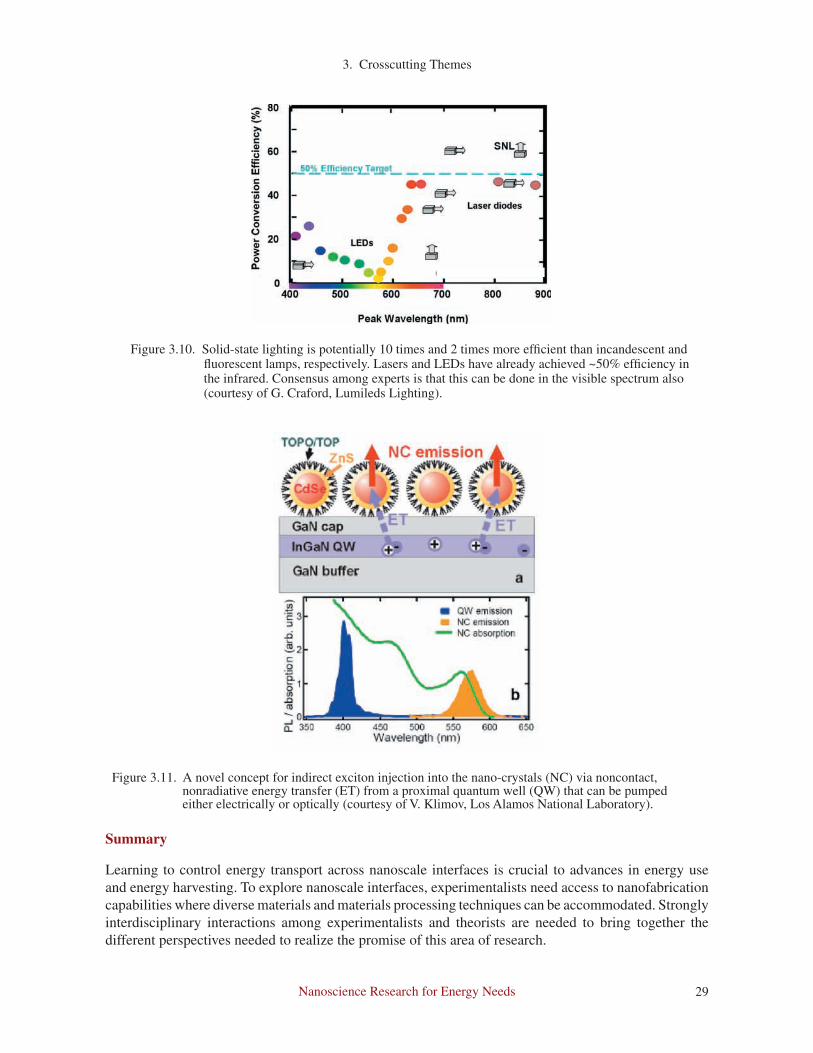
Nanoscience Research for Energy Needs 29
3. Crosscutting Themes
Summary
Learning to control energy transport across nanoscale interfaces is crucial to advances in energy use and energy harvesting. To explore nanoscale interfaces, experimentalists need access to nanofabrication capabilities where diverse materials and materials processing techniques can be accommodated. Strongly interdisciplinary interactions among experimentalists and theorists are needed to bring together the different perspectives needed to realize the promise of this area of research.
Figure 3.10. Solid-state lighting is potentially 10 times and 2 times more efficient than incandescent and fluorescent lamps, respectively. Lasers and LEDs have already achieved ~50% efficiency in the infrared. Consensus among experts is that this can be done in the visible spectrum also (courtesy of G. Craford, Lumileds Lighting).
Figure 3.11. A novel concept for indirect exciton injection into the nano-crystals (NC) via noncontact, nonradiative energy transfer (ET) from a proximal quantum well (QW) that can be pumped either electrically or optically (courtesy of V. Klimov, Los Alamos National Laboratory).

Nanoscience Research for Energy Needs30
3. Crosscutting Themes
LINKING STRUCTURE AND FUNCTION AT THE NANOSCALE
Vision
The new phenomena and properties that emerge as materials are constructed at the nanometer scale are at the foundation of nanoscience. These properties originate from the fact that nanoscale materials, consisting of only 100–10,000 atoms, have unique structures that cannot be extrapolated from our understanding of traditional bulk materials that we have routinely used in daily life. These properties include, for example, reactivity for more efficient catalytic fuel production (hydrocarbon, H, solar) and for removal of environmental pollutants such as sulfur dioxide, and mechanical strength for ultra-light and strong composite materials. At the heart of this functionality is the structure of the nanomaterial. Understanding this relationship between structure and function will allow us to develop synthesis techniques that optimize structure and will ultimately lead to the creation of functional nanomaterials by design.
State of the Art
A primary difference between nanoscale particles and bulk materials is the fraction of atoms at the surface or interface. Nearly all the atoms of a nanoparticle are at the surface or interface. This results in atomic composition and structure not found in macroscopic materials. Atomic bonds at surfaces and interfaces are distorted as compared to bulk materials. The high fraction of surface atoms leads to segregation phenomena that are highly sensitive to the size of the nanoparticle. This structural uniqueness leads to remarkable physical properties. For example, gold in its bulk form is chemically inert. However, nanoparticles of gold on a titania substrate exhibit remarkable catalytic properties, such as the ability to oxidize the hazardous gas carbon monoxide (see sidebar on page 31) and decompose sulfur dioxide, a primary source of acid rain and smog. In fact the efficiency of this material is 10 times greater than that of commercial catalysts used in today’s automobile catalytic converters for the decomposition of sulfur dioxide. Similarly, the discovery of nanostructured carbon, such as carbon nanotubes, opens the door to the development of a new class of mechanical and electronic materials. Their structure leads to an unprecedented tensile strength-to-weight ratio and can lead to new composite materials based on these properties. Furthermore, the detailed carbon structure of the tube (chirality) leads to carbon nanotubes (CNTs) that are conducting or semiconducting (sidebar on page 32). Future applications of these properties include efficient energy transmission and nano-electronics.
These two examples also serve to highlight the range of our understanding of the coupling between structure and function. The detailed atomic and electronic structure of CNTs are known to a large extent. Characterization of the relationship between the atomic chirality of the tube and its electronic properties is well known and has led to a detailed understanding of the electronic band structure that is derived both by quantum mechanical calculations and experimental measurements (see sidebar, page 32). On the other hand, a detailed picture of the atomic structure of gold nanoparticles on titania does not exist. Present characterization techniques only allow the measurement of cluster sizes, but not the atomic structure of the cluster or the more important cluster surface. Without this vital information, high-quality, theoretical calculations of chemical reactivity of this system are impossible and advances must rely on intuition or serendipitous discovery.

Nanoscience Research for Energy Needs 31
3. Crosscutting Themes
Catalysis by Gold Nanoclusters on Supports
Although bulk gold is known for being unreactive, gold present in the form of nanoparticles on porous supports such as TiO2 has surprisingly been found to be a highly active catalyst for oxidation of CO [36]. Gold catalysts could be of value in automotive fuel cell applications, because CO in hydrogen streams to fuel cells poisons the fuel cell catalyst, and it could be removed by catalytic oxidation. Some data show an optimum catalytic activity when the nanoclusters are about 3 nm in diameter. The unique catalytic properties of gold nanoclusters may be related to size-dependent electronic properties of the nanoclusters. Continuing research is pointing to a more complicated picture. The catalytic activity of supported gold has been found to depend on the support, the treatment conditions, and the presence of water, prompting investigators to probe samples during catalysis of CO oxidation with X-ray absorption spectroscopy at synchrotrons. The data give evidence of cationic gold present with the gold nanoclusters. It still remains to be determined how the catalysis is infl uenced by the interface between the gold nanoclusters and the support, where the gold may be cationic, and by the presence of isolated gold cations too small to have been imaged with the nanoclusters. Continuing research with combinations of spectroscopic methods and imaging of functioning catalysts and theory are required to unlock the secrets of gold catalysts. The effi ciency of this material for the decomposition of sulfur dioxide is 10 times greater than that of commercial catalysts used in today’s automobile catalytic converters [37].
Hard Problems
Building the Science
The overarching challenge that we face in designing novel nanomaterials is establishing the physical and chemical principles that relate the changes in molecular structure to the functionality that emerges at nanometer length-scales. Because we lack these principles, new nanoscale phenomena are being discovered experimentally at an ever-increasing rate that is far outpacing advances in our physical understanding. Effects of quantum confi nement, the enhancement of interfacial free energies over bulk free energies, and the importance of surface states have all been recognized since the inception of nanoscience, but a complete theoretical treatment of these factors has yet to emerge. Moreover, many effects of nanoscale structure have only just begun to be explored theoretically, such as fl uid fl ow in nanoporous structures for which the electric double layer is less than the pore size.
Gold nanoparticles and their reactivity (portions © 1998 AAAS; reprinted by permission [36]).
Correlation of the catalytic activity with the percentage and surface concentration of cationic and zero valent gold supported on MgO.
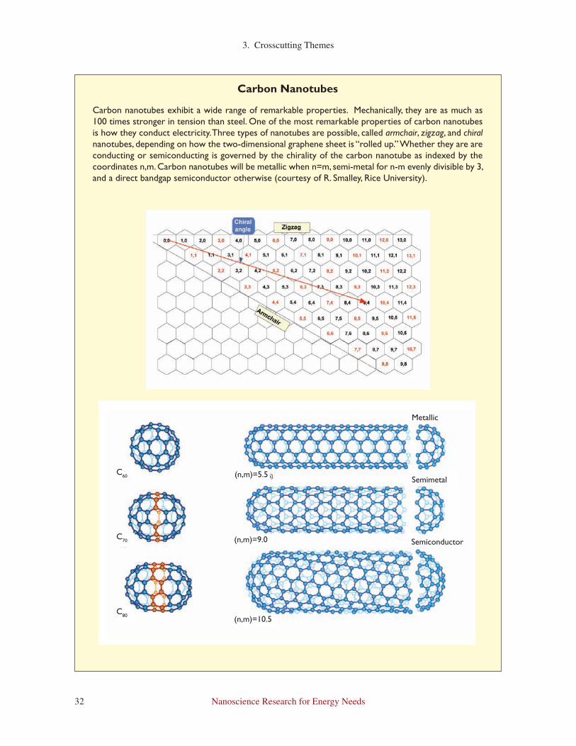
Nanoscience Research for Energy Needs32
3. Crosscutting Themes
Carbon Nanotubes
Carbon nanotubes exhibit a wide range of remarkable properties. Mechanically, they are as much as 100 times stronger in tension than steel. One of the most remarkable properties of carbon nanotubes is how they conduct electricity. Three types of nanotubes are possible, called armchair, zigzag, and chiral nanotubes, depending on how the two-dimensional graphene sheet is “rolled up.” Whether they are are conducting or semiconducting is governed by the chirality of the carbon nanotube as indexed by the coordinates n,m. Carbon nanotubes will be metallic when n=m, semi-metal for n-m evenly divisible by 3, and a direct bandgap semiconductor otherwise (courtesy of R. Smalley, Rice University).
Metallic
(n,m)=5.5
(n,m)=9.0
(n,m)=10.5
Semiconductor
SemimetalC60
C70
C80

Nanoscience Research for Energy Needs 33
3. Crosscutting Themes
One of the discoveries that has emerged from recent research is that the impact of nanoscale structure on function extends beyond individual nanoscale elements to hierarchical architectures. This is because length-dependent factors such as the proximity of interfaces become comparable to the length scale of electron, exciton, and phonon transport. As a result, dramatic enhancements in properties emerge. Some specific examples include creation of nanocrystal thin-film composites that increase the efficiency of photo-induced energy transfer to as much as 100%, nanolaminated solids to depress thermal transport below what was previously called the minimum thermal conductivity, and self-organized arrays of nanoscale structures on alloy films to enhance catalytic reactivity.
3D Time and Spatially Resolved Chemical, Physical, and Functional Imaging of Nanomaterials and Devices
Detailed information on the structure and dynamics of the nanoscale components of a functional nanosytem is as essential to the development of nanotechnology as the understanding of the individual parts of a complex machine or factory are to development of macrotechnology. In particular, experimental data on the “local” chemical and physical state of a nanosystem as a function of location and time in a functioning device will be necessary before advanced “modeling tools” are developed for complex nanosystems such as solar cells, fuel cells, or complex nanobiochemical sensors. Indeed, spatially and temporarily resolved data of this type are a prerequisite for advanced engineering and design in nanotechnology. Three-dimensional time and spatially resolved chemical, physical, and functional imaging is particularly challenging since the most critical regions of a nanosystem are located at interfaces between dissimilar materials that are deeply embedded in a device and, as a result, unavailable to most characterization techniques in surface science.
A promising approach to this challenge is the invention of new experimental techniques that directly combine and correlate two or more spectroscopy and imaging tools in a single method. One of the first techniques to achieve 3D chemical kinetic imaging in a nanosystem is the recently introduced technique for investigating the local optoelectronic properties of organic and inorganic semiconductor nanoparticles embedded in a functioning device that involves simultaneous single molecule spectroscopy (SMS) and controllable oxidation/reduction in an electronic device. This technique (denoted by fluorescence voltage single molecule spectroscopy, F-V/SMS) is analogous to current vs. voltage (I-V) measurements for devices and electrochemical cells. F-V/SMS data are reported for single molecules (nanoparticles) of the conjugated polymer MEH-PPV as a function of bias voltage on the device and bias sweep rate to obtain information on both the energetics and kinetics of the charge transfer (oxidation/reduction) process in situ on the nanoscale.
In an F-V/SMS experiment, SMS data are acquired while simultaneously subjecting the single molecule (or nanoparticle) to repetitive oxidation/reduction. F-V/SMS has the unique capability of measuring the “local” energetics, dynamics, and chemical kinetics of single nanoparticles embedded in a functioning electronic device.
A simple F-V/SMS example is presented in the figure, which shows the fluorescence intensity of a single isolated ~10 nm conjugated polymer molecule (MEH-PPV) as a function of the bias voltage V on the device. F-V/SMS offers a unique means for characterizing intermediates in the photochemistry and photophysics of MEH-PPV in a device, at the molecular level, analogous to the way electrochemical measurements are used to study reaction intermediates in solution.
F-V/SMS data for MEH-PPV in hole-injection device. The gray layer in the device is an insulator. The layer labeled HTL is the hole transporting layer (courtesy of P. Barbara, Univ. of Texas).

Nanoscience Research for Energy Needs34
3. Crosscutting Themes
Advanced Scanning Probe Systems
Advances in scanned probe systems make it possible to incorporate multiple functions for both synthesis and characterization at nanometer length scales even solid-liquid interfaces. Functions available in a single instrument include: topographic imaging, single molecule optical spectroscopy, nanolithography, and force spectroscopy. (a) Surface of calcium phosphate dihydrate. (b) Image of fluorescing single molecules and time correlation emission probability from one molecule. (c) 30 nm lines of amino-terminated alkane thiols. (d) Force curves representing three different stages of interaction between tip and surface following protein-carbohydrate binding (courtesy of C. Orme, T. Huser, C. Hollars, C. Talley, C. Cheung, J. De Yoreo, T. Ratto, and M. McElfresh, Lawrence Livermore National Laboratory).
At a very fundamental level, structure and function are magnifiers of the evolution in the energetic drivers that occurs as materials dimensions are reduced. This is because the thermodynamic and kinetic factors that determine pathways of materials formation and both the morphology and stability of structures depend exponentially on those drivers. In many respects, it is for this reason that nanoscience is such a rich source of new phenomena. Developing a comprehensive understanding of the physical and chemical principles that lead to these phenomena will remain a major challenge for the foreseeable future.
Developing the Tools
Characterization tools always have been key drivers in both developing new routes to materials synthesis as well as understanding novel properties and physical phenomena. Because nanomaterial building blocks consist of only tens to thousands of atoms and molecules, in order to understand the relationship between structure and function we require tools with a commensurate level of resolution, preferably at the single-molecule level. Because the function of nanomaterials depends so strongly on the state of the interface, whether in contact with vapor, liquid, or solid, these tools must have the capability to image in three dimensions (3D) at buried interfaces. Moreover, to understand the structure-function relationship, one would like the capability to measure both structure and function simultaneously. Finally, because fluctuations in structure become increasingly important as the scale of materials decreases, understanding energy conversion and transport requires a time-dependent structure measurement capability with time-resolution on the scale of the thermal fluctuations (1013 Hz).
The ability to bring such capabilities to bear on nanomaterials would impact both the rate of development and the enhancement of properties. Perhaps in more than any other area, investment in this next generation

Nanoscience Research for Energy Needs 35
3. Crosscutting Themes
of characterization tools provides leverage for all other areas of investment. Without measurement and characterization, theory and simulation cannot be validated, synthesis and fabrication cannot be evaluated, and enhancements in performance cannot be demonstrated. With these tools, development in all other areas will accelerate.
While the past two decades have seen the development of powerful new characterization tools such as the scanning probe microscope, we are a long way from achieving the capability outlined above. For example, although one of the premier tools of nanoscience, the scanning tunneling microscope (STM), can be used to image individual atoms, its use is restricted to relatively flat, conducting surfaces. Even the seemingly simple challenge of imaging the surface atomic structure of a pure metal nanoparticle —such as the gold catalyst particles described above—has not been solved, due to the high curvature of the surface. Clearly, the problem of experimentally determining the structure-function relationship of a quantum dot, for which the structure of the interface between the inorganic component and the surface passivation layer is central in determining optical performance, is well out of reach of this instrument. Moreover, the STM is severely limited for obtaining subsurface information. Similarly, the other tools at our disposal have serious limitations: Neutron scattering can be used to obtain three-dimensional information, but the resolution is far above the molecular level. Transmission electron microscopy sees internal structure with atomic resolution, but can not handle surface structure or interfaces that are deeply buried or in contact with vapor and fluid environments. Other limitations prevent the application of single-molecule confocal microscopy, X-ray diffraction, and ion mass spectrometry from reaching the desired level of performance.
Although it is unlikely that any one instrument can provide all of the capabilities outlined above, one can conceive of advances in many of the existing tools that, when taken in composite, will give a much more complete picture of the molecular structure and evolution in nanoscale materials.
Theory and Modeling
Although theory, modeling, and simulation have seen tremendous advances in the last 10 years, nanostructures and their function present challenges that cannot be addressed presently. These fall into two broad categories: (1) high fidelity calculations of atomic and electronic structure, and (2) linking this information to predicting functionality. A major contributor to the first challenge is the complexity of nanostructures that derives from their structural non-periodicity and chemical heterogeneity. For the second challenge, the lack of reliable and quantitative measurements (see section above) makes benchmarking of new techniques and approaches nearly impossible. However, the development of our ability to model and predict the function of nanostructures will be a determining factor in the success of nanotechnology for energy applications.
As an example, we are not presently able to calculate accurately the structure of supported nanoclusters on surfaces. The immediate ramification of this is that we do not understand the origin of the catalytic behavior of the nanoparticle gold/titania system and how it relates to the structure of the particle surface and the interface. Even further from our reach is the ability to calculate the pathways and energy barriers for chemical reactions on these particles.
A major goal of our efforts should be to develop theory, modeling, and computational capabilities that will permit the prediction and design of functional nanostructures. This will enable the rational design of new materials for a wide range of important energy applications.

Nanoscience Research for Energy Needs36
3. Crosscutting Themes
ASSEMBLY AND ARCHITECTURE
Vision
Meeting the needs of energy applications over the next decade will require new classes of nanostructured materials capable of functionalities and efficiencies far beyond what is currently considered state of the art. Research will be needed to provide the linkage between the needed functions and the attainable architectures. Furthermore, novel strategies for assembly of pre-designed architectures will be required to make possible the fabrication of these architectures, initially in small quantities, but eventually in bulk. In order for nanoscale architecture to provide needed capabilities for energy applications in both the near and long term, we will need to overcome significant technological barriers.
Over the next decade, investment in fundamental studies of the properties of nanostructured materials and the methods for assembly of these materials will fuel development of methods that will allow the following capabilities:
Step-by-Step Epitaxial Growth of Complex Self-Assembled Materials and Hierarchical Structures
New solution-based approaches have been developed to grow complex self-assembled materials and nanostructures epitaxially. This approach is based on controlled nucleation and growth and on a multi-step, sequential growth process that switches the solution chemistry between each step. In each step, the nanostructures are formed epitaxially on the structures produced in the previous step. However, the general principles have not been established to apply to a wide range of materials (courtesy of J. Liu, Sandia National Laboratories).
Molecular controland ordering
Nanometer assembly High order assemblyand growth
Large scaleintegration

Nanoscience Research for Energy Needs 37
3. Crosscutting Themes
1. Prediction of nanoscale architectures that will achieve extraordinary and novel material properties for energy applications. These efforts will include design of materials with novel functionalities that allow us to greatly improve the efficiency of:
- Transport of mass and energy - Energy storage - Energy conversion - Energy production2. Appropriate control of the architecture of materials at the nanoscale to make possible fabrication of
structures predicted to exhibit desirable functions.
3. Development of programmed assembly processes to implement cost-effective fabrication of the structures predicted to exhibit desirable functionalities.
4. Engineering of architectures that integrate nanoscale capabilities into micro and macroscale systems that address energy applications and needs. Full incorporation of nanostructured materials will drive redesign of macro systems to take optimal advantage of these material properties.
State of the Art
Living systems provide a proof of principle that programmed assembly of nanoscale components can be integrated into complex, functional structures and applied to macroscale systems. Studies of the directed assembly of virus particles have provided some insight into the logic of the processes that result in these viruses. Although biological systems may have been the origin of the concept of self-assembly, most complex biomolecular systems assemble through processes in which a greater degree of control can be applied. This frequently requires the participation of accessory proteins that guide or catalyze portions of the assembly process [38]. By examining the assembly of viral protein coats and other biological structures, researchers have identified a set of principles that are important to biological systems’ ability to program the assembly of complex architectures. The key principles [38, 39] include:
• Controlled conformational switching (allowing individual components to turn interaction potentials on and off)
• Construction by linear pathways (where the sequence of events is programmed just as we would assemble the axles before adding wheels to a car)
• Assembly from subassemblies (to span multiple length scales)
• Common building blocks to build different structures (contributes to efficiency in synthesis and production)
• Use of templates and jigs for form determination
• Staged assembly (makes sure that subassemblies are added in the appropriate sequence)
Achieving Complete Control of Assembly at the Molecular Level
Biomolecular systems are capable of exquisite control of assembly processes in which nanoscale particles (e.g., proteins) assemble themselves to form complex, functional, macromolecular machines. Attempts to emulate this process using biomimetic or self-assembling systems have led to numerous functional developments including multilayers, two-dimensional arrays of nanoparticles, and nanostructured materials.
Although many of these structures have properties important for the application of nanotechnology to energy needs, they fall short of the ultimate goal of complete three-dimensional control of architecture at
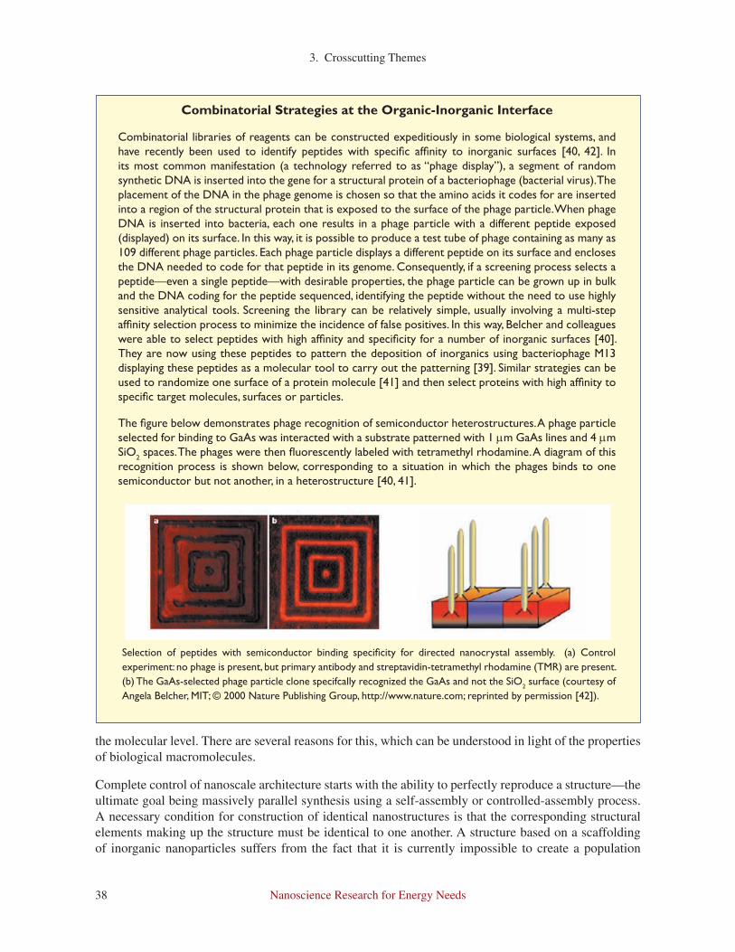
Nanoscience Research for Energy Needs38
3. Crosscutting Themes
Combinatorial Strategies at the Organic-Inorganic Interface
Combinatorial libraries of reagents can be constructed expeditiously in some biological systems, and have recently been used to identify peptides with specific affinity to inorganic surfaces [40, 42]. In its most common manifestation (a technology referred to as “phage display”), a segment of random synthetic DNA is inserted into the gene for a structural protein of a bacteriophage (bacterial virus). The placement of the DNA in the phage genome is chosen so that the amino acids it codes for are inserted into a region of the structural protein that is exposed to the surface of the phage particle. When phage DNA is inserted into bacteria, each one results in a phage particle with a different peptide exposed (displayed) on its surface. In this way, it is possible to produce a test tube of phage containing as many as 109 different phage particles. Each phage particle displays a different peptide on its surface and encloses the DNA needed to code for that peptide in its genome. Consequently, if a screening process selects a peptide—even a single peptide—with desirable properties, the phage particle can be grown up in bulk and the DNA coding for the peptide sequenced, identifying the peptide without the need to use highly sensitive analytical tools. Screening the library can be relatively simple, usually involving a multi-step affinity selection process to minimize the incidence of false positives. In this way, Belcher and colleagues were able to select peptides with high affinity and specificity for a number of inorganic surfaces [40]. They are now using these peptides to pattern the deposition of inorganics using bacteriophage M13 displaying these peptides as a molecular tool to carry out the patterning [39]. Similar strategies can be used to randomize one surface of a protein molecule [41] and then select proteins with high affinity to specific target molecules, surfaces or particles.
The figure below demonstrates phage recognition of semiconductor heterostructures. A phage particle selected for binding to GaAs was interacted with a substrate patterned with 1 µm GaAs lines and 4 µm SiO2 spaces. The phages were then fluorescently labeled with tetramethyl rhodamine. A diagram of this recognition process is shown below, corresponding to a situation in which the phages binds to one semiconductor but not another, in a heterostructure [40, 41].
Selection of peptides with semiconductor binding specificity for directed nanocrystal assembly. (a) Control experiment: no phage is present, but primary antibody and streptavidin-tetramethyl rhodamine (TMR) are present. (b) The GaAs-selected phage particle clone specifcally recognized the GaAs and not the SiO2 surface (courtesy of Angela Belcher, MIT; © 2000 Nature Publishing Group, http://www.nature.com; reprinted by permission [42]).
the molecular level. There are several reasons for this, which can be understood in light of the properties of biological macromolecules.
Complete control of nanoscale architecture starts with the ability to perfectly reproduce a structure—the ultimate goal being massively parallel synthesis using a self-assembly or controlled-assembly process. A necessary condition for construction of identical nanostructures is that the corresponding structural elements making up the structure must be identical to one another. A structure based on a scaffolding of inorganic nanoparticles suffers from the fact that it is currently impossible to create a population

Nanoscience Research for Energy Needs 39
3. Crosscutting Themes
of these particles that are completely identical to one another. Huge numbers of identical biological macromolecules can be readily synthesized, suggesting their potential utility as scaffolds for assembly of a nanoscale structure.
A second requirement for control of nanoscale architecture is the ability to design interacting surfaces that bind tightly with high specificity. Although design of interacting surfaces is beyond the capabilities of molecular biology, it is possible to create combinatorial libraries of molecules from which molecules with the desired binding properties can be selected. This approach works well for the immune system and for a wide variety of biotechnology applications. It is also beginning to work well for selection of biological molecules that bind tightly not only to other biological systems, but to a broad range of inorganic materials. It will soon be possible to design and construct structural elements made up of biological macromolecules that have desired geometry and binding specificity, and assemble them into nanoscale structures that incorporate both organic and inorganic elements.
As an example of this approach, Kischenko et al. (Fig. 3.12) used the filamentous bacteriophage M13 as a scaffold for constructing a 30 nm diameter, hollow iron cylinder. Native M13 is a flexible cylinder approximately 6.5 nm in diameter and one micrometer in length and is made up largely of 2,600 copies of a major coat protein. This protein was chemically modified by covalent attachment of two biotin molecules to each coat protein. Biotin binds non-covalently to a protein, streptavidin, with very high affinity. Consequently, when streptavidin was added to the virus particles, it coated the entire exterior of the particles, creating a particle with a diameter about double that of the original virus particle. Since streptavidin is a tetramer, this construct exhibited many biotin binding sites on its surface, which could be used to add additional structural elements. An iron storage protein, ferritin, was modified by covalent binding of biotin, and the biotinylated ferritin was added to the streptavidin-coated phage particles. This resulted in a final cylinder about 30 nm in diameter, the outer layer of the cylinder being very rich in iron enclosed in the ferritin molecules (see Fig. 3.12).
This particular example uses the very high affinity of streptavidin for biotin to achieve linkage of elements that do not normally interact. An alternative would be the use of elements selected from combinatorial libraries as outlined above.
While these principles provide important clues for programming assembly of multi-functional structures, the principles themselves do not tell us how to design systems that can demonstrate these characteristics.
Figure 3.12. Left: Electron micrographs of biotinlylated M13, streptavidin-coated M13, and the final ferritin-coated structure. Right: The diagram depicts the final structure in cross section and from the side (courtesy of Kischenko, Davidovich, and Makowski, Argonne National Laboratory).

Nanoscience Research for Energy Needs40
3. Crosscutting Themes
Currently, much progress is being made in exploring assembly processes in purely synthetic and nano/bio hybrid systems. Examples include liquid crystals, Languimir-Blodgett and lipid bilayers, quantum dot arrays, lyotropic systems (block co-polymers), and positioning of nanocrystals within protein or DNA frameworks. For example, lyotropic assembly is routinely used to template the structure of mesoporous silica structures that are already used as industrial catalysts. Assembly in these systems is driven by hydrophilic/hydrophobic interactions, local mechanical strain gradients, and molecular templating interactions. Even though a theoretical underpinning for these interactions is in many cases well established, our ability to predict the structure and properties that will result from a many-body assembly process remains poorly developed.
It is interesting to note that natural systems do not always depend on diffusion to bring the proper nanoscale components into place. In fact, nanoscale machines (motor proteins) are used to transport nanoscale components into their proper place in multiscale architectures. Very recent work is now exploring the use of motor proteins as a means of transporting quantum dots within large-scale architectures. While this work is in a very early stage and borrows heavily upon the machinery made available in living systems, results are already contributing to our understanding of self-repairing and adaptive-system architectures.
Just because nature assembles everything from the nanoscale up does not mean that we should do the same with all materials. Photolithography and other patterning tools can be used to create multi-scale architectures in combination with bottom-up assembly. In fact, the combination of nanoscale assembly within micro or macroscale architectures is likely to dominate the early applications. As an example, the energy efficiency of mechanical machinery can be greatly increased by reducing friction and wear. This problem has dramatic consequences in microscale machinery where interfacial forces dominate mechanical response. Current state of the art for microelectromechanical systems (MEMS) uses an organized molecular layer (about two nm thick) to prevent direct adhesion and contact between moving parts. In this case the nano-assembly enhances performance of the microscale-device architecture. However, one could imagine the machine architectures that might result if the multifunctional property of the nano-assembly (e.g., modulating surface energy) were used as a design principle.
The ultimate value of multifunctional nanomaterials may be seen in the way that they impact the architecture of the engineering system. Today, a limited number of nanostructured materials exist and only a tiny portion of that multifunctional systems design can be explored. However, nano-inspired system architectures are already developing. For example, energy-transfer mechanisms that can be made highly efficient at the nanoscale are leading to new approaches for converting electrical energy into visible lighting.
Energy systems inherently demand multiscale architecture. For example, energy conversion often involves charge separation that is best accomplished at the nanoscale. That charge—whether it be for a photovoltaic application, a battery, or a thermoelectric device—must be collected and distributed at the micro and even macroscale. In the same way, catalysis is inherently nanoscale, involving the detailed position and arrangement of atoms and molecules at the reaction center. Once again, the demands of moving chemical feedstock and reaction products into and out of the nanoscale region requires organization on multiple length scales.
Important questions remain:
• What spectrum of functions can be achieved by building nanoscale materials?
• How can small collections of nanocomponents be combined and arranged to generate new functions?
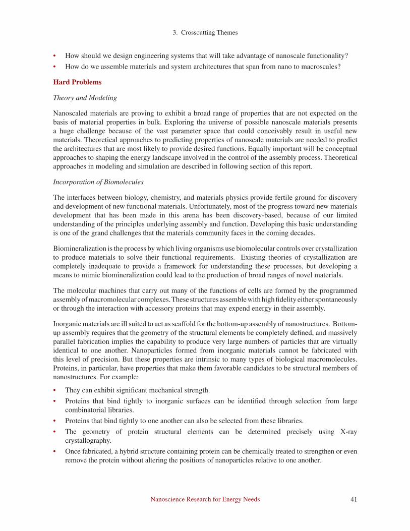
Nanoscience Research for Energy Needs 41
3. Crosscutting Themes
• How should we design engineering systems that will take advantage of nanoscale functionality?
• How do we assemble materials and system architectures that span from nano to macroscales?
Hard Problems
Theory and Modeling
Nanoscaled materials are proving to exhibit a broad range of properties that are not expected on the basis of material properties in bulk. Exploring the universe of possible nanoscale materials presents a huge challenge because of the vast parameter space that could conceivably result in useful new materials. Theoretical approaches to predicting properties of nanoscale materials are needed to predict the architectures that are most likely to provide desired functions. Equally important will be conceptual approaches to shaping the energy landscape involved in the control of the assembly process. Theoretical approaches in modeling and simulation are described in following section of this report.
Incorporation of Biomolecules
The interfaces between biology, chemistry, and materials physics provide fertile ground for discovery and development of new functional materials. Unfortunately, most of the progress toward new materials development that has been made in this arena has been discovery-based, because of our limited understanding of the principles underlying assembly and function. Developing this basic understanding is one of the grand challenges that the materials community faces in the coming decades.
Biomineralization is the process by which living organisms use biomolecular controls over crystallization to produce materials to solve their functional requirements. Existing theories of crystallization are completely inadequate to provide a framework for understanding these processes, but developing a means to mimic biomineralization could lead to the production of broad ranges of novel materials.
The molecular machines that carry out many of the functions of cells are formed by the programmed assembly of macromolecular complexes. These structures assemble with high fidelity either spontaneously or through the interaction with accessory proteins that may expend energy in their assembly.
Inorganic materials are ill suited to act as scaffold for the bottom-up assembly of nanostructures. Bottom-up assembly requires that the geometry of the structural elements be completely defined, and massively parallel fabrication implies the capability to produce very large numbers of particles that are virtually identical to one another. Nanoparticles formed from inorganic materials cannot be fabricated with this level of precision. But these properties are intrinsic to many types of biological macromolecules. Proteins, in particular, have properties that make them favorable candidates to be structural members of nanostructures. For example:
• They can exhibit significant mechanical strength.
• Proteins that bind tightly to inorganic surfaces can be identified through selection from large combinatorial libraries.
• Proteins that bind tightly to one another can also be selected from these libraries.
• The geometry of protein structural elements can be determined precisely using X-ray crystallography.
• Once fabricated, a hybrid structure containing protein can be chemically treated to strengthen or even remove the protein without altering the positions of nanoparticles relative to one another.
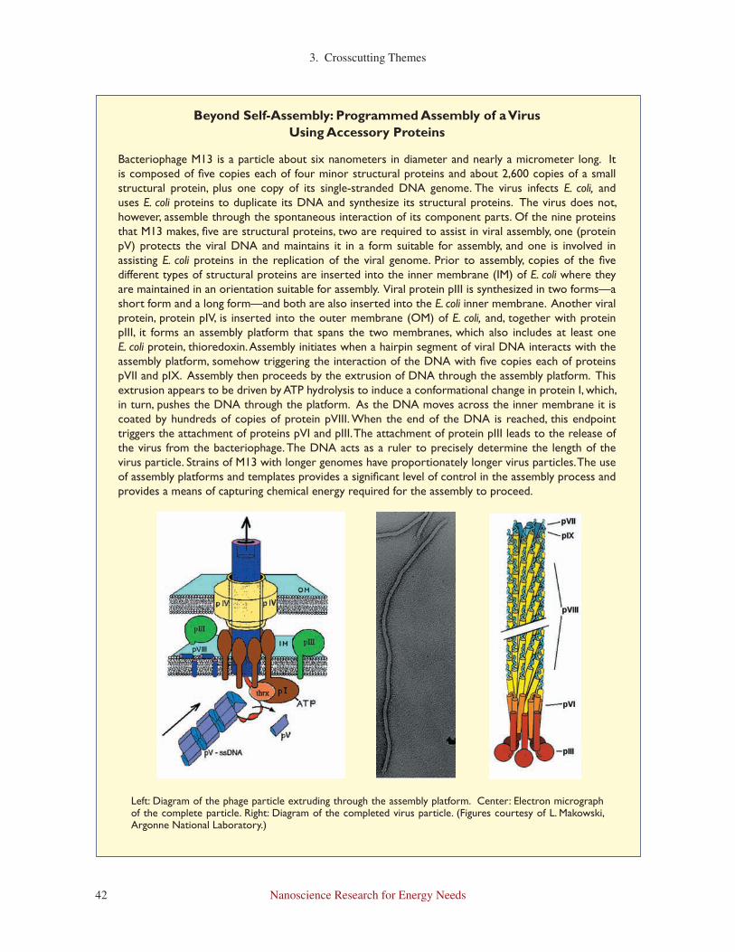
Nanoscience Research for Energy Needs42
3. Crosscutting Themes
Beyond Self-Assembly: Programmed Assembly of a Virus Using Accessory Proteins
Bacteriophage M13 is a particle about six nanometers in diameter and nearly a micrometer long. It is composed of five copies each of four minor structural proteins and about 2,600 copies of a small structural protein, plus one copy of its single-stranded DNA genome. The virus infects E. coli, and uses E. coli proteins to duplicate its DNA and synthesize its structural proteins. The virus does not, however, assemble through the spontaneous interaction of its component parts. Of the nine proteins that M13 makes, five are structural proteins, two are required to assist in viral assembly, one (protein pV) protects the viral DNA and maintains it in a form suitable for assembly, and one is involved in assisting E. coli proteins in the replication of the viral genome. Prior to assembly, copies of the five different types of structural proteins are inserted into the inner membrane (IM) of E. coli where they are maintained in an orientation suitable for assembly. Viral protein pIII is synthesized in two forms—a short form and a long form—and both are also inserted into the E. coli inner membrane. Another viral protein, protein pIV, is inserted into the outer membrane (OM) of E. coli, and, together with protein pIII, it forms an assembly platform that spans the two membranes, which also includes at least one E. coli protein, thioredoxin. Assembly initiates when a hairpin segment of viral DNA interacts with the assembly platform, somehow triggering the interaction of the DNA with five copies each of proteins pVII and pIX. Assembly then proceeds by the extrusion of DNA through the assembly platform. This extrusion appears to be driven by ATP hydrolysis to induce a conformational change in protein I, which, in turn, pushes the DNA through the platform. As the DNA moves across the inner membrane it is coated by hundreds of copies of protein pVIII. When the end of the DNA is reached, this endpoint triggers the attachment of proteins pVI and pIII. The attachment of protein pIII leads to the release of the virus from the bacteriophage. The DNA acts as a ruler to precisely determine the length of the virus particle. Strains of M13 with longer genomes have proportionately longer virus particles. The use of assembly platforms and templates provides a significant level of control in the assembly process and provides a means of capturing chemical energy required for the assembly to proceed.
Left: Diagram of the phage particle extruding through the assembly platform. Center: Electron micrograph of the complete particle. Right: Diagram of the completed virus particle. (Figures courtesy of L. Makowski, Argonne National Laboratory.)

Nanoscience Research for Energy Needs 43
3. Crosscutting Themes
Implementation Strategies
Deeply interdisciplinary approaches are required to take advantage of the huge potential of biological systems to assemble nanostructures that exhibit a very broad range of functional properties. Training is perhaps the greatest barrier to progress in this area. Biologists and materials scientists usually are trained to ask profoundly different kinds of questions: Biologists are untrained in the materials properties that are important for providing the functionality of nanodevices; materials scientists know little of the tools and techniques of molecular biology required to make use of biological approaches. Novel funding mechanisms that encourage the collaboration of molecular biologists and materials scientists to study assembly mechanisms and the organic-inorganic interface through sharing of students may provide a grass-roots approach to the problem. Alternately, cross-training of mature scientists through sabbaticals and visiting appointments also has potential to impact this important intellectual cross-fertilization.
Scientific and Technological Infrastructure Needs
Infrastructure to enable the growth of theoretical and experimental research into assembly and architecture and the bio-inorganic interface will be critical to taking advantage of the huge opportunities that exist at this interface. The development of facilities that include resources for both molecular biology and materials research in close proximity will greatly expedite the path forward, both by making possible experiments that require profoundly different sets of tools and by connecting scientists with very different types of expertise. In addition to the usual array of instrumentation for characterization of nanostructured materials and particles, it will be important to develop state-of-the-art transmission electron microscopy for exploring the geometry of the nanostructures created. This should be augmented by X-ray and neutron scattering to characterize, as completely as possible, the geometry of the structure created during an assembly process. Computational approaches will require extensive computer power to predict the physical properties of nanostructures and to determine the optimal geometries that should be the goals of the assembly process. Feedback between experimental determination of physical properties of real structures and theoretical predictions will help in optimization of computer approaches to the prediction of nanostructure properties, aiding in progressive advancement of nanostructure design principles.
Priorities and Conclusions
Biomolecular systems have great potential to act as models for the bottom-up assembly of nanostructures and nanostructured materials. They provide a basis for developing a set of principles to guide bottom-up assembly of nanostructured systems, and can act as scaffolds for the placement of inorganic nanoparticles as a step toward the construction of complex nanodevices. They have great potential as units in nanostructures for several reasons: Huge populations of biomolecules can be created that are entirely identical to one another. Furthermore, huge combinatorial libraries of biomolecules with one face randomized can be created, and, from those libraries, molecules that exhibit high affinity for a particular molecular target can be selected. Once a molecule with a desired specificity of binding is identified, it can be reproduced exactly and in huge numbers using simple tools of molecular biology.
Materials science has the potential to predict the properties of nanoparticles and provide guidance as to the structures that will have desirable functions. Furthermore, many of the characterization tools of materials research are applicable to bio-inorganic systems.
Taking full advantage of the potential of biological systems to impact technological approaches to assembly will require a determined effort to foster collaborations among researchers and students involved in molecular biology and materials science. Possible approaches include housing them in shared facilities and providing them with interdisciplinary training and instrumentation.

Nanoscience Research for Energy Needs44
3. Crosscutting Themes
The scale ranges from • to ••••• to indicate relative importance.
TMS Needs for Future Energy SecurityUnderlying TMS capabilities 1 2 3 4 5 6
Methods for bridging temporal and spatial scales • ••• •••• •• ••••• •••••Many-body electronic structure calculations ••••• • ••••• ••••• ••• ••••Electron transport including interfaces ••••• • •••• ••••• •• ••••Electronic structure methods for optical properties •••• •••• ••• ••••• •• •••
Table 3.1Relationships between Advances in Underlying TMS Capabilities and Their Relative
Impact on the TMS Needs for Future Energy Security
THEORY, MODELING, AND SIMULATION FOR ENERGY NANOSCIENCE
Vision
As anticipated in initial planning for the National Nanotechnology Initiative (NNI) [43], the combination of theory, modeling, and simulation (TMS) is playing a crucial role throughout nanoscience [44]. As we look to meet nanoscience challenges and enable our future energy security, we have identified the following six TMS needs relevant to the high-impact research directions that emerged from the workshop:
1. Provide insight into nanoscale experimental measurements
2. Understand function and the impact of dynamics and fluctuations
3. Characterize new materials (including catalysts) virtually
4. Quantify transport mechanisms (including electron transport) at the nanoscale
5. Predict self-assembly
6. Design and virtually synthesize new materials (including optoelectronic materials)
Today, the TMS capabilities to meet these needs exist in varying degrees of maturity and have been listed approximately in order from most to least mature. Satisfying all of these needs will require substantial investment in fundamental research in theory, simulation methodologies, and algorithms. In particular, among the TMS capabilities for future research investment identified in [44], four stand out as particularly relevant to the TMS needs for future energy security:
1. Methods for bridging temporal and spatial scales
2. Many-body electronic structure calculations
3. Electron transport including interfaces
4. Electronic structure methods for optical properties
The impact of each focus area on the six TMS needs identified above is summarized in the table below. Applying many of these capabilities will require calculations on leadership-class high-performance computers. The remainder of this section describes the state of the art in each of these focus areas, and the barriers that must be overcome in order to achieve progress, concluding with a description of a paradigm for developing a computational infrastructure in support of nanoscience as part of DOE’s new ultrascale computing initiative.

Nanoscience Research for Energy Needs 45
3. Crosscutting Themes
Methods for Bridging Temporal and Spatial Scales
Nanotechnology is particularly challenging because to make devices useful at the macroscopic scale, we have to understand how properties at the nanoscale impact behavior at the macroscale; likewise, we need to know how, during synthesis, manipulation of variables at the macroscale affects nanoscale structure. This interaction between different levels of spatial and temporal detail becomes acute in nanotechnology more routinely than in any other area of computational materials science or computational chemistry. This is especially the case in developing devices (e.g., energy conversion devices) for meeting energy needs, since the scale of the problem suggests large-scale solutions. Significant challenges exist in incorporating important atomic-scale details into simulations that reach macroscopic length and time scales. Applications that could benefit from such capabilities include chemical reactor design for processing and conversion of fuel-related molecules and for synthesizing solid-state lighting, predicting and modeling self-assembly, linking atomic-scale structure of catalysts with reactivity and selectivity, modeling separations, and synthesizing materials to realize separations. Great strides have been made in bridging length and time scales both through serial coupling of scales (involving separate simulations at each relevant scale) and through parallel coupling (with simultaneous, interacting simulations at different scales).
In dynamic, solid-state simulations involving rare-event dynamics, advances in capabilities for rapidly detecting transition states and performing on-the-fly kinetic Monte Carlo simulations are promising for achieving long-time simulations in areas such as catalysis, transport in porous materials, and thin-film epitaxy. However, these simulations do not yet reach far beyond the nanometer spatial scale, and their cost can become prohibitive if ab initio potentials are involved. On the other hand, in simulations of rapid crack propagation in solids, large length scales have been included by coupling simultaneous simulations at the quantum, atomic, and continuum scales. However, these simulations do not extend far beyond the picosecond time scale. To predict and characterize new materials, we must develop the capability to seamlessly bridge both spatial and temporal scales.
Multiple Length Scale Simulations of Crack Propagation in Silicon
Simultaneous simulations coupling quantum-mechanical tight-binding molecular dynamics (MD) with classical MD based on empirical force fields and continuum finite-element methods show plastic deformation modes that cannot be predicted using any of these approaches alone.
The silicon slab shown here is decomposed into the five different dynamic regions of the simulation: the continuum finite-element (FE) region, the atomistic molecular-dynamics (MD) region, the quantum tight-binding (TB) region, the FE-MD ‘‘handshaking’’ region, and the MD-TB ‘‘handshaking’’ region. The image shows the simulated silicon slab, with expanded views of the FE-MD (orange nodes-blue atoms) interface and the TB (yellow atoms) region surrounded by MD (blue atoms). Note that the TB region surrounds the crack tip with broken-bond MD atoms trailing behind this region. The acronym, MAAD, implies ‘‘macroatomistic ab initio dynamics” (© 1999 American Physical Society; reprinted by permission [45]).

Nanoscience Research for Energy Needs46
3. Crosscutting Themes
Novel Energy-Efficient Separations
At the end of the 20th century, energy consumption by U.S. industry was estimated to be 35 quadrillion BTUs (quads) per year, of which 6 quads were consumed by separation processes. Hence, replacing high-energy-usage separation methods by less energy-intensive methods—such as membrane separation or adsorption—would result in substantial future energy savings.
Nanoporous materials can be extremely useful in separations because of their ability to recognize and discriminate between molecules; examples include zeolites and activated carbons. Nanoporous metal-organic frameworks materials (MOFs) also have emerged recently as promising new candidates for adsorption and membrane separations [46]. They may be considered as analogs of zeolites, but with all of the chemical diversity of carbon compounds. MOFs are formed via directed assembly of metal or metal-oxide vertices connected by organic linker molecules, as shown by the examples in the figure. A large variety of structures has been produced, ranging from extended crystalline structures to discrete molecular triangles, squares, cubes, and chains. Molecular modeling is a particularly effective tool in providing guidance about new structures before they are synthesized. Modeling can predict relative rates of diffusion (important for membrane separations) and selectivity for adsorption of guest molecules from mixtures. Modeling can also provide insight into molecular-level details and the structure of molecules in the nanopores.
The figure at right shows two examples of metal-organic materials synthesized in a directed-assembly process. Top: Schematic representation of the assembly process. Middle: building blocks and the resulting three-dimensional frameworks of different MOFs [47]; empty lines at the ZnO4 vertices indicate where linkers bind. One complete, larger cavity of each MOF framework is shown, with transparent blue spheres added to illustrate cavity size. Bottom: Building blocks for representative molecular squares [48]. (Figure courtesy of Randall Snurr, Northwestern Univ., © 2004 John Wiley & Sons, Inc.; reprinted by permission [46].)
Molecular squares
pyrazinemolecular
square
bipyridinemolecular
square
porphyrinmolecular
square
A second challenge in multiscale modeling for energy applications lies in predicting self-assembly of nanoscale building blocks. Challenges in this area lie in accurately resolving, through first-principles calculations, the relative contributions of various interactions, including van der Waals dispersion forces, hydrogen bonding, and dynamic structure and chemistry at nanoparticle surfaces. Understanding how these forces affect solvation, depletion, and phase behavior in seamless, multiscale models is also a challenge. Efficient simulation techniques, such as multi-canonical simulations, need to be developed to reliably predict the phase behavior of assemblies.
Many-Body Electronic Structure Calculations
Electronic structure calculations are ubiquitous in energy applications, which inevitably involve conversions from one form of matter or energy to another (e.g., catalysis). To realize the full potential of computational modeling and simulation in understanding and controlling chemical change, significant theoretical, mathematical, and computational obstacles must be overcome. Simulations must reliably
IRMOF-1 IRMOF-6 IRMOF-14
MOF materials
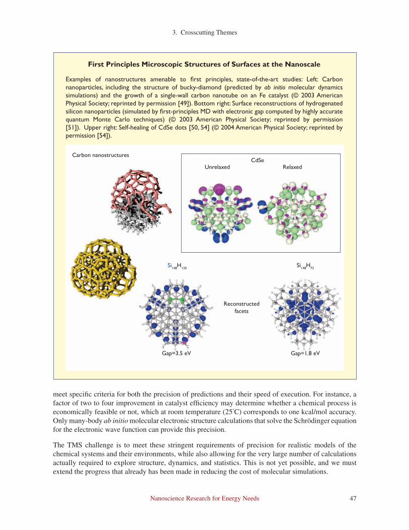
Nanoscience Research for Energy Needs 47
3. Crosscutting Themes
First Principles Microscopic Structures of Surfaces at the Nanoscale
Examples of nanostructures amenable to fi rst principles, state-of-the-art studies: Left: Carbon nanoparticles, including the structure of bucky-diamond (predicted by ab initio molecular dynamics simulations) and the growth of a single-wall carbon nanotube on an Fe catalyst (© 2003 American Physical Society; reprinted by permission [49]). Bottom right: Surface reconstructions of hydrogenated silicon nanoparticles (simulated by fi rst-principles MD with electronic gap computed by highly accurate quantum Monte Carlo techniques) (© 2003 American Physical Society; reprinted by permission [51]). Upper right: Self-healing of CdSe dots [50, 54] (© 2004 American Physical Society; reprinted by permission [54]).
CdSeUnrelaxed Relaxed
Carbon nanostructures
Si148H72
Gap=1.8 eV
Si148H120
Gap=3.5 eV
Reconstructed facets
meet specifi c criteria for both the precision of predictions and their speed of execution. For instance, a factor of two to four improvement in catalyst effi ciency may determine whether a chemical process is economically feasible or not, which at room temperature (25°C) corresponds to one kcal/mol accuracy. Only many-body ab initio molecular electronic structure calculations that solve the Schrödinger equation for the electronic wave function can provide this precision.
The TMS challenge is to meet these stringent requirements of precision for realistic models of the chemical systems and their environments, while also allowing for the very large number of calculations actually required to explore structure, dynamics, and statistics. This is not yet possible, and we must extend the progress that already has been made in reducing the cost of molecular simulations.

Nanoscience Research for Energy Needs48
3. Crosscutting Themes
In addition, current approaches to forming reduced models of large systems (e.g., embedding small quantum regions in larger classical models) are at best heuristic; reliable techniques are needed to bridge between electronic structure calculations and higher-level methods.
Electron Transport, Including Interfaces
The application of nanoscience to meeting future energy needs will inevitably result in the development of nanoscale devices that transport electrons, particularly across interfaces that may be of quite dissimilar character (e.g., electron transport from a biological molecule to a metal contact across a nano-interface). At the nanoscale, new electron transport phenomena come into play, and classical descriptions become inadequate in the face of quantum phenomena such as tunneling, fluctuations, confined dimensionality, and the discreteness of the electric charge. Additionally, nanoscale devices typically will be dominated entirely by surfaces. This presents further complications for electronic materials, which often undergo strong and complex reconstructions. At the theory and simulation level, there does not exist today a consensus on the correct methodology for calculating electron transport in the presence of large electric fields (as would be the case, for example, in nanoelectronics devices), and the difficulty of the corresponding experiments means that validation of methods is difficult. An additional problem in electron transport across interfaces is that often the interfaces are not characterized at all, hence the need to resort to computational “construction” of interfaces, i.e., using simulation methods to perform computational nanoscale “experiments” to produce interface structures that should be expected in the experimental systems. Having produced a putative interface, the electron transport is then calculated, recognizing that this, in fact, may result in further structural changes to the interface. Hence, the process of developing a model for the interface and performing electron transport calculations is iterative in nature.
While the discussion above focuses on a specific example, the difficulty of designing clean and conclusive experiments on poorly characterized systems, and the problem of uncertain methodology, are ubiquitous in electron transport studies at the nanoscale. Resolution of these problems will come from significant investments both in TMS and in experiments. The return on this investment will be tools that enable the design of new nanoscale devices for energy applications.
Electronic Structure Methods for Optical Properties
Exploiting the optical properties of nanostructures can have significant impact on future energy needs – for example, reducing energy consumption for lighting by replacing current technologies with solid-state lighting or organic light-emitting diodes (described in the energy manipulation section). At nanoscale dimensions, optical properties of matter are often dramatically altered. For example, while bulk silicon has poor optical properties for optoelectronic devices such as solar cells or lasers, at small dimensions the band gap in silicon can be blue-shifted from the infrared to the optical region; as a result, porous silicon exhibits remarkable room-temperature luminescence. To capitalize properly on such phenomena, a deeper quantitative understanding of the optical properties of matter will be required.
One of the theoretical challenges to understanding optical properties and excitations is that most commonly used methods for calculating structural energies, such as density functional theory, are not well suited for predicting excited-state properties. The problem is exacerbated for nanoscale systems, where the many-body effects are enhanced by the physical confinement of the excitation. New theoretical techniques and computational methodologies focused on optical properties, as well as complementary experimental validation, are required to develop the design tools needed to predict optical properties of nanostructures on a routine basis.

Nanoscience Research for Energy Needs 49
3. Crosscutting Themes
Computational Infrastructure in Support of Nanoscience
The diversity of methods used in computational nanoscience, combined with the need for high-performance computing infrastructure to solve realistic problems in nanoscience, pose a considerable challenge. Consequently, many codes have to be optimized on new computer architectures and used in a tightly coupled manner. Interdisciplinary teams need to be formed among scientists who have not typically collaborated and shared codes previously. In view of the many person-years that have to be invested to develop a specific method and computer code, it is quite clear that in order to make computational nanoscience a tool for discovery, algorithm and software developments need to be explicitly coordinated to allow for seamless integration and re-use of methods and the corresponding computer codes. A concerted effort is therefore needed to create community-based software repositories and computational endstations, which are analogous to endstations in large experimental facilities (e.g., a powder-diffraction endstation attached to a large neutron-scattering facility) for nanoscience that will allow scientists to create new simulation methods and respond quickly to the emerging needs of nanoscience (see sidebar below).
Computational Endstation for Nanoscience
Conceptual vision for computational endstations “attached” to leadership class supercomputing facilities. Source: “The Roadmap for the Revitalization of High-End Computing” (courtesy of D.A. Reed, Computing Research Asssociation, www.cra.org).
Facilities Analogy

Nanoscience Research for Energy Needs50
3. Crosscutting Themes
In such a repository one would, for example, reduce different electronic structure methods to kernels that use a common interface and input/output system. Users as well as other codes that implement a particular aspect of nanoscience, such as electron transport, optical properties, etc., would access these kernels though the common interface. Methods and the corresponding kernels that are best suited for a specific computer architecture can then be selected, optimized, and maintained in a computational endstation. This would allow optimal use of high-performance computing infrastructure while keeping the entire software repository flexible enough to satisfy the changing requirements of theory, modeling, and simulation as the field of nanoscience develops.
In May 2004, DOE announced that Oak Ridge National Laboratory and Argonne National Laboratory will together host a leadership-class scientific computing facility (LCSCF) intended to be the most powerful computing facility in the world, surpassing Japan’s Earth Simulator. It will be dedicated to capability computing (i.e., solving outstanding problems that can only be addressed in a sufficiently timely and scientifically rigorous way by such a large computing facility). Included in the proposal for the LCSCF is support for computational endstations. One of the proposed endstations will support computational nanoscience through the enhancement, optimization, and support of community-based codes for the major classes of calculations used in computational nanoscience, through the development of XML-based standards for data interchange between codes and the development of validated, re-usable libraries. Significant investment in the LCSCF endstation for nanoscience from DOE’s Office of Basic Energy Sciences and Office of Advanced Scientific Computing Research is expected over the coming years.

Nanoscience Research for Energy Needs 51
3. Crosscutting Themes
SCALABLE SYNTHESIS
Uniqueness of Nanomaterials
Nanomaterials are important because they can add new functionalities that are simply not present in bulk materials. These may result from (1) high surface area (large surface-to-volume ratio), (2) new intrinsic properties due to small size (quantum size effects) or shape (high aspect ratio and reduced dimensionality), and (3) intimate nanoscale connectivity conferring directionality and minimizing losses in energy transport. These new “nano” functionalities can provide electrical and thermal conductivity, field emission, and catalyst support or gas adsorption properties unrivalled by bulk materials. Consequently, the synthesis of functional nanomaterials offers a unique opportunity to make the breakthrough discoveries and truly revolutionary developments that are needed to meet the energy challenge.
Goals for Synthesis
The synthesis of functional nanomaterials, that is, materials systems able to deliver greatly enhanced properties at the macro scale where they are needed, entails several interrelated challenges in the quality, quantity, variety, and integrated design and assembly of nanomaterials:
• The quality challenge requires synthesizing defect-free nanomaterials with sufficiently high purity that their ultimate properties can be reliably measured and accurately known. From them, baseline data will be obtained for subsequently controlling synthesis and designing materials systems to deliver their enhanced properties.
• The quantity challenge requires developing, understanding, and optimizing readily scalable methods of synthesis for economical, large-scale production of high-quality nanomaterials.
• The variety challenge requires research and development of methods to efficiently explore and expand the “library” of enhanced nanomaterials properties that are potentially available. The current library is small and the broad range of potential nanomaterials mostly unexplored.
• The integrated design and assembly (or “nano-to-bulk”) challenge requires developing means of synthesis compatible with subsequent (or, better yet, concurrent) assembly of nanomaterials into systems or architectures that exhibit the greatly enhanced nanoscale properties at the macroscale.
With these goals, basic research is clearly the central need for the synthesis of practical nanomaterials leading to fabrication/processing and system-design techniques that preserve unique nanoscale properties while coupling them to the macroscale. So where does nanomaterials synthesis stand, relative to where it needs to be?
Vision for Nanomaterials Synthesis
Compared with the needs described, the present state of nanomaterials synthesis can be summarized as follows: (1) rewarding insights were obtained from limited use of in situ optical and spectroscopic diagnostics during growth processes, (2) there is relatively slow feedback from characterization (properties measurements) and the experimental search for new materials, and (3) there is slower feedback from theory and modeling to understand and improve nanomaterials synthesis. Three key conclusions can be made:
1. In situ time-resolved diagnostic methods to understand the synthesis and mechanisms of growth of nanomaterials have proven tremendously valuable. Increased investment specifically for in situ monitoring techniques could have a disproportionately large payoff in understanding and controlling synthesis.

Nanoscience Research for Energy Needs52
3. Crosscutting Themes
2. There is little capability for designing optimized nanomaterials. This defi cit is pointed out because fabricating practical materials with enhanced nanoscale properties could soon be assisted by theory, modeling, and simulation, by taking advantage of ongoing advances in computational nanoscience on leadership computers. The parallel development of modeling and simulation (multiscale modeling and virtual synthesis, leading to materials by design), and of time-resolved in situ diagnostics of fabrication/processing techniques, is essential in understanding and controlling the synthesis of complex, natural, engineered nanomaterials systems.
3. There is particular need to explore more rapidly the vast space of nanomaterials that are potentially available with new and novel properties. This exploration could be accomplished much more effi ciently by development of: (a) characterization methods that combine imaging with in situ properties measurements and sample manipulation, so that the results of synthesis could be evaluated quickly; and (b) computational methods to guide the search for novel materials, thereby limiting the space that must be searched experimentally.
These recognitions lead to a vision of synthesis as the key, yet probably the limiting, step in what should be a tightly connected loop of synthesis, characterization, theory/modeling/simulation, and design. This loop (Fig. 3.13) can be traversed repeatedly until the objectives in synthesis, quality, quantity, variety, and integrated design have been met.
Synthesis Research Directions
There are two important underlying themes in the energy impact of nanomaterials:
1. It is implicit in many of the research recommedations in a recent report from the Department of Energy’s Basic Energy Sciences Advisory Committee that degradation of materials in extreme environments (particularly high temperature) is a formidable barrier to developing new energy resources with moderate-to-low initial cost and a long operating lifetime. Consequently, processes must be discovered and systems developed that can operate at low temperatures [3].
2. There is an opportunity for revolutionary advances through establishing new methods to fabricate materials, including nanoscale self-assembly.
This section identifi es some directions in research on nanomaterials synthesis that potentially have the highest impact on U.S. energy security.
Figure 3.13. The feedback loop of synthesis/characterization/modeling/design.

Nanoscience Research for Energy Needs 53
3. Crosscutting Themes
Carbon Nanotube Materials Synthesis
Carbon nanotubes have stimulated intense interest because of their remarkable electrical, optical, and mechanical properties. Single-walled carbon nanotubes (SWNTs) or “buckytubes” are the most famous of all new nanoscale materials. An SWNT is most easily thought of as a polymer of hexagonal carbon rings, or a single giant molecule composed of pure carbon, whose properties go far beyond those of the earlier miracle polymers, nylon, polypropylene, polyester, and Kevlar. Like them, it is expected that SWNTs ultimately will be produced at a level of millions of pounds per year in chemical plants worldwide. The tubes grow from low-cost carbon feedstocks, such as carbon monoxide, methane, or methanol in contact with a nanoscale catalyst particle attached to the end of each growing tube. The first commercial applications are expected within a few years. Buckytubes are famously expected to be incredibly strong, perhaps with a tensile strength as much as 100 times greater than steel. No doubt this great strength will lead to super-strong, lightweight materials with major applications, but their initial most critical property will be that these new buckytubes conduct electricity. Each tube is uniquely identified by a diameter and two integers, n and m, that specify its “chirality” (or amount of twist). If n=m, the tube is a metallic one-dimensional quantum conductor. If n-m is evenly divisible by three, the tube is a semimetal; otherwise, it is a direct bandgap semiconductor with a bandgap similar to gallium arsenide. The combination of mechanical, electrical, and optical properties of buckytubes, together with their extremely high thermal conductivity, is expected to lead to their extensive use as multifunctional materials in future energy systems.
The key opportunity for high-impact research in synthesizing nanotubes is to establish a practical method to produce them with perfect control of their diameter, length, and chirality, corresponding to producing SWNTs with the same value of n and m. The challenge is to do this from a cheap feedstock, such as syngas (CO + H
2) made from coal, with a process that can be scaled to produce millions of pounds per
year inexpensively. This would allow fabrication of buckytube electrical transmission lines. Spun as a continuous fiber by a process similar to Kevlar, an all-buckytube carbon fiber is expected to have an electrical conductivity at least as high as that of copper (perhaps much higher) at only one-sixth the weight. This high conductivity derives from both the highly efficient transmission of electrons down the individual tubes that act as quantum wave guides in one direction, and the efficient resonant-quantum tunneling of the electrons from tube to tube as the current passes down the fiber. Meeting this challenge will provide the basis for low-cost and highly efficient (low-loss) massive electrical power transmission over continental and intercontinental distances. A global buckytube electrical grid, combined with cost-effective photovoltaic cells for converting solar energy to electricity, would go a long way toward providing clean, carbon-free energy, and simultaneously reducing the need to store energy by generating electricity continuously on Earth’s sunny side.
Among the other interesting properties of carbon nanotubes is their remarkably high material strength. Carbon nanotube fibers are applicable for super-tough multifunctional electronic textiles, as illustrated in Figure 3.14. “Toughness” is a measure of the energy needed to rupture a fiber. Spider silk has long set the standard, with toughness five times higher than the same mass of steel. But now there is a new standard: 100-meter-long composite fibers recently spun from single-walled carbon nanotubes in a gel matrix were tougher than any natural or synthetic fiber [55]. Moreover, the fibers are easy to sew and weave into textiles, resulting in a host of promising electronic-textile applications, including distributed sensors, electrical interconnects, and super-capacitors and batteries.
Nanocrystal Synthesis
Advances in synthetic chemistry have enabled researchers to make a variety of narrowly dispersed nanocrystals, each small enough to exhibit quantum confinement effects. By tuning the size of the
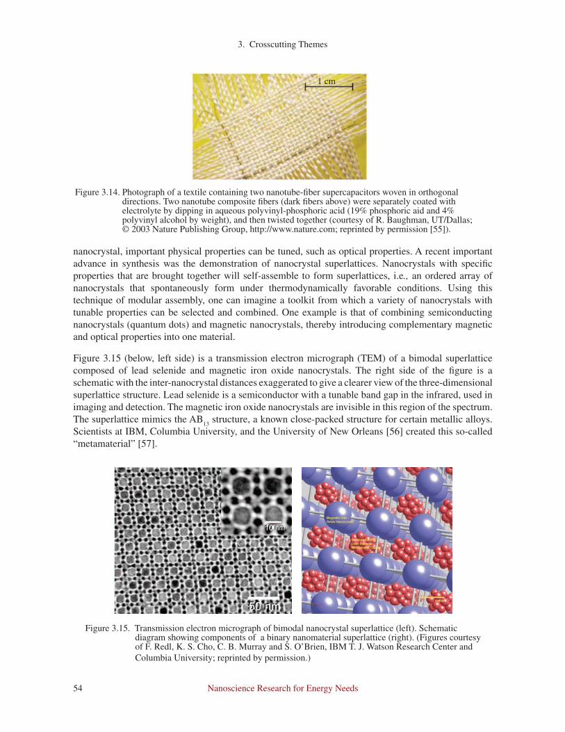
Nanoscience Research for Energy Needs54
3. Crosscutting Themes
nanocrystal, important physical properties can be tuned, such as optical properties. A recent important advance in synthesis was the demonstration of nanocrystal superlattices. Nanocrystals with specifi c properties that are brought together will self-assemble to form superlattices, i.e., an ordered array of nanocrystals that spontaneously form under thermodynamically favorable conditions. Using this technique of modular assembly, one can imagine a toolkit from which a variety of nanocrystals with tunable properties can be selected and combined. One example is that of combining semiconducting nanocrystals (quantum dots) and magnetic nanocrystals, thereby introducing complementary magnetic and optical properties into one material.
Figure 3.15 (below, left side) is a transmission electron micrograph (TEM) of a bimodal superlattice composed of lead selenide and magnetic iron oxide nanocrystals. The right side of the fi gure is a schematic with the inter-nanocrystal distances exaggerated to give a clearer view of the three-dimensional superlattice structure. Lead selenide is a semiconductor with a tunable band gap in the infrared, used in imaging and detection. The magnetic iron oxide nanocrystals are invisible in this region of the spectrum. The superlattice mimics the AB
13 structure, a known close-packed structure for certain metallic alloys.
Scientists at IBM, Columbia University, and the University of New Orleans [56] created this so-called “metamaterial” [57].
Figure 3.15. Transmission electron micrograph of bimodal nanocrystal superlattice (left). Schematic diagram showing components of a binary nanomaterial superlattice (right). (Figures courtesy of F. Redl, K. S. Cho, C. B. Murray and S. O’Brien, IBM T. J. Watson Research Center and Columbia University; reprinted by permission.)
Figure 3.14. Photograph of a textile containing two nanotube-fi ber supercapacitors woven in orthogonal directions. Two nanotube composite fi bers (dark fi bers above) were separately coated with electrolyte by dipping in aqueous polyvinyl-phosphoric acid (19% phosphoric aid and 4% polyvinyl alcohol by weight), and then twisted together (courtesy of R. Baughman, UT/Dallas; © 2003 Nature Publishing Group, http://www.nature.com; reprinted by permission [55]).
1 cm

Nanoscience Research for Energy Needs 55
3. Crosscutting Themes
Figure 3.16. Charge separation in 20 basepair-long oligonucleotides in TiO2/DNA hybrids monitored by
silver deposition. Secondary hole trapping site GG was separated by different distances from the nanoparticle’s surface, so altering the effi ciency of silver deposition. These measurements indicate that, in these hybrid systems, photo-generated holes can be transported to very large separation distances (up to ~80 Å) (courtesy of G. Woloschak, Northwestern Univ.; © 2003 Nature Publishing Group, http://www.nature.com; reprinted by permission [58]).
Synthesis of Bio-Nanomaterial Hybrids
Using biological approaches enables interesting new directions in synthesizing materials relevant to energy issues. One example of this challenge and opportunity is in creating a new approach for artifi cial photochemical energy conversion based on functionally integrated hybrid (nanoparticle-biomolecule) semiconductor conjugates.
Biomolecule-semiconductor conjugates are exceptional in the way that they carry out energy capture and subsequent chemical/electrical conversion [58]. Rajh and coworkers at Argonne National Laboratory have created a new family of semiconductor-based artifi cial photosynthetic systems that duplicate the primary light-induced charge separation mechanism in natural photosynthesis. This new class of functional hybrid materials is composed of specifi cally designed nanoparticles that combine the robustness and photo-responsiveness of inorganic materials with the recognition properties of biological molecules. Their synthesis exploits the discovery that the surface of metal-oxide nanocrystalline particles differs from that of the respective bulk materials, and is characterized by a highly reactive under-coordinated surface.
Using this approach, hybrid conjugates of TiO2 nanoparticles and DNA oligonucleotides were synthesized,
thereby changing the intrinsic properties of the semiconductor and generating new hybrid molecular orbitals, so making the optical properties of metal-oxide nanoparticles tunable throughout the entire visible region. Additionally, as in natural photosynthesis, these hybrid nanocrystallites display weak electronic coupling of fully separated charges, thus channeling effi cient extended charge separation. Insight into charge separation was obtained through measuring the effi ciency of photocatalytic silver reduction.
Figure 3.16 illustrates the extended charge separation. The amount of photocatalytic deposition of metallic silver decreases with increasing separation between the TiO
2 surface and secondary

Nanoscience Research for Energy Needs56
3. Crosscutting Themes
GG hole acceptor. This dependence follows an exponential decay with a low attenuating exponent coeffi cient of 0.045. Consequently, photo-generated holes are transported to a very large separation distance of ~80 Å. This enhanced charge separation is attributed to the fact that upon excitation of the TiO
2/dopamine system, charge pairs are instantaneously separated by distances of
~20 Å. This large initial separation diminishes the probability of their recombination, so that holes may be trapped at secondary hole acceptors at very large distances apart.
Ternary and More Complex Nanomaterials Synthesis
An area of great opportunity for high impact on the nation’s energy security involves expanding the library of functional nanomaterials. For example, the perovskite oxide family of materials exhibits a wide variety of interesting properties in the bulk phase, including high-temperature superconductivity, colossal magnetoresistance, ferroelectricity, and piezoelectric behavior. Recently, several groups have started examining strategies for synthesizing this important class of nanomaterials.
One example of the state of the art in this fi eld is the recent progress in the nanomaterial synthesis of the ternary perovskite oxides. Utilizing a solid-state synthesis approach, well-dispersed nanocubes of the high dielectric constant oxide SrTiO
3 and nanowires of the ferroelectric BaTiO
3 have been made [59].
Figure 3.17 shows electron micrographs of the perovskite nanomaterials. The barium titanate synthesis (left image) generates nanorods of diameter ~50 nm and several micrometers long, while the strontium titanate synthesis (right image) results in nanocubes with an edge length of ~80 nm. These syntheses yield perovskite nanomaterials of very high purity and crystallinity. In addition, this solid-state synthesis approach can be scaled up to produce gram quantities of nanomaterials. It also offers promise for a variety of nanomaterials in the perovskite-oxide family.
Combinatorial Techniques and Highly Parallel Sorting
A major synthesis challenge is to rapidly and effi ciently search through materials with new compositions or structures to reveal the relatively few phases with greatly enhanced properties or especially useful new combinations of them. For nanomaterials, the follow-on challenges are to optimize conditions for synthesis and to develop scaled-up methods to produce the quantities needed for energy applications, while maintaining quality and key properties.
An example of a synthesis process that can permit rapid screening is continuous compositional spread methods of synthesizing fi lms using pulsed laser deposition (PLD-CCS) for complex oxides [60, 61].
Figure 3.17. Solid-state synthesis of perovskite nanoparticles. (A) BaTiO3 nanorods, (B) SrTiO
3 nanocubes
(© 2003 American Chemical Society; reprinted by permission [59]).

Nanoscience Research for Energy Needs 57
3. Crosscutting Themes
By placing an aperture in front of the ablation target, and combining this with precisely controlling synchronization between the firing of the pulsed laser, exchanging of the ablation target, and translating/rotating the substrate, both the film’s thickness and deposition energetics constant were maintained across the entire compositional range. Moreover, the resulting compositional spread covered a sufficiently large area that the continuously varying film properties could be measured by conventional methods such as SQUID magnetometry, electrical resistivity, and ellipsometry. This PLD-CCS technique was demonstrated by growing an Sr
xCa
1-xRuO
3 binary alloy with “x” varying from zero to one, and with
properties ranging from a metallic ferromagnet (x=1) toward antiferromagnetism (x=0) (Fig. 3.18).
Figure 3.18. Sr and Ca compositions of an SrxCa
1-xRuO
3 composition-spread film, plotted as a function of
substrate position, as determined by EDX and RBS. Excellent agreement is obtained between designed and actual compositions (© 2004 Elsevier; reprinted by permission [61]).
The versatility of the PLD-CCS method, and its potential for the discovery and optimization of nanoscale catalysts, recently was demonstrated by applying it to discover the optimum Fe-Mo catalyst composition for growing long dense forests of elongated multiwall carbon nanotubes. A two-dimensional compositional spread of Fe-Mo catalyst, consisting of “wedges” of Fe and Mo with their thickness increasing orthogonally, was deposited on an Al-coated Si wafer, followed by CVD growth of multiwall carbon nanotubes. Rapid optical profiling determined the nanotubes’ height as a function of position, and SEM verified their continuity. A clear dependence was found on the catalyst’s composition, not simply a threshold amount of one constituent, and nanotubes were grown an order of magnitude longer than in previous state-of-the-art experiments [62].
These examples demonstrate that non-equilibrium combinatorial search-and-discovery methods such as PLD-CCS reveal broad trends from a single-film growth run, whereas conventional methods require many samples, much more time, and lose precision because of run-to-run irreproducibility. Further development of such economical and high throughput combinatorial and sorting/optimization methods is needed, both to efficiently search for nanomaterials and to scale up their production to the quantities needed for energy applications.
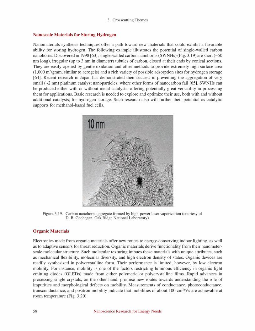
Nanoscience Research for Energy Needs58
3. Crosscutting Themes
Nanoscale Materials for Storing Hydrogen
Nanomaterials synthesis techniques offer a path toward new materials that could exhibit a favorable ability for storing hydrogen. The following example illustrates the potential of single-walled carbon nanohorns. Discovered in 1998 [63], single-walled carbon nanohorns (SWNHs) (Fig. 3.19) are short (~50 nm long), irregular (up to 3 nm in diameter) tubules of carbon, closed at their ends by conical sections. They are easily opened by gentle oxidation and other methods to provide extremely high surface area (1,000 m2/gram, similar to aerogels) and a rich variety of possible adsorption sites for hydrogen storage [64]. Recent research in Japan has demonstrated their success in preventing the aggregation of very small (~2 nm) platinum catalyst nanoparticles, where other forms of nanocarbon fail [65]. SWNHs can be produced either with or without metal catalysts, offering potentially great versatility in processing them for applications. Basic research is needed to explore and optimize their use, both with and without additional catalysts, for hydrogen storage. Such research also will further their potential as catalytic supports for methanol-based fuel cells.
Organic Materials
Electronics made from organic materials offer new routes to energy-conserving indoor lighting, as well as to adaptive sensors for threat reduction. Organic materials derive functionality from their nanometer-scale molecular structure. Such molecular texturing imbues these materials with unique attributes, such as mechanical fl exibility, molecular diversity, and high electron density of states. Organic devices are readily synthesized in polycrystalline form. Their performance is limited, however, by low electron mobility. For instance, mobility is one of the factors restricting luminous effi ciency in organic light emitting diodes (OLEDs) made from either polymeric or polycrystalline fi lms. Rapid advances in processing single crystals, on the other hand, promise new routes towards understanding the role of impurities and morphological defects on mobility. Measurements of conductance, photoconductance, transconductance, and positron mobility indicate that mobilities of about 100 cm2/Vs are achievable at room temperature (Fig. 3.20).
Figure 3.19. Carbon nanohorn aggregate formed by high-power laser vaporization (courtesy of D. B. Geohegan, Oak Ridge National Laboratory).
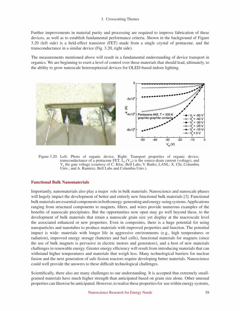
Nanoscience Research for Energy Needs 59
3. Crosscutting Themes
Further improvements in material purity and processing are required to improve fabrication of these devices, as well as to establish fundamental performance criteria. Shown in the background of Figure 3.20 (left side) is a fi eld-effect transistor (FET) made from a single crystal of pentacene, and the transconductance in a similar device (Fig. 3.20, right side).
The measurements mentioned above will result in a fundamental understanding of device transport in organics. We are beginning to exert a level of control over these materials that should lead, ultimately, to the ability to grow nanoscale heteroepitaxial devices for OLED-based indoor lighting.
Figure 3.20. Left: Photo of organic device. Right: Transport properties of organic device; transconductance of a pentacene FET. Isd (Vsd) is the source-drain current (voltage), and Vg the gate voltage (courtesy of C. Kloc, Bell Labs; V. Butko, LANL; X. Chi, Columbia Univ.; and A. Ramirez, Bell Labs and Columbia Univ.).
Functional Bulk Nanomaterials
Importantly, nanomaterials also play a major role in bulk materials. Nanoscience and nanoscale phases will hugely impact the development of better and entirely new functional bulk materials [3]. Functional bulk materials are essential components in both energy-generating and energy-using systems. Applications ranging from structural components to magnets, fi lters, and wires provide numerous examples of the benefi ts of nanoscale precipitates. But the opportunities now open may go well beyond these, to the development of bulk materials that retain a nanoscale grain size yet display at the macroscale level the associated enhanced or new properties. Even in composites, there is a huge potential for using nanoparticles and nanotubes to produce materials with improved properties and function. The potential impact is wide: materials with longer life in aggressive environments (e.g., high temperatures or radiation), improved energy storage (batteries and fuel cells), functional materials for magnets (since the use of bulk magnets is pervasive in electric motors and generators), and a host of new materials challenges in renewable energy. Greater energy effi ciency will result from introducing materials that can withstand higher temperatures and materials that weigh less. Many technological barriers for nuclear fusion and the next generation of safe fi ssion reactors require developing better materials. Nanoscience could well provide the answers to these diffi cult technological challenges.
Scientifi cally, there also are many challenges to our understanding. It is accepted that extremely small-grained materials have much higher strength than anticipated based on grain size alone. Other unusual properties can likewise be anticipated. However, to realize these properties for use within energy systems,

Nanoscience Research for Energy Needs60
3. Crosscutting Themes
it is necessary to preserve the structure and unique properties of nanocrystals and nanoprecipitates, which are often only metastable throughout their fabrication and use.
Nanoscale Enhancements of Bulk Materials Properties for Energy Applications
An example of the application of nanoscience to bulk materials is the recent development of a ferritic oxide-dispersive-strengthened (ODS) Fe-12Cr-3W-0.4Ti+0.25Y
2O
3 (wt %) alloy, which contains a
secondary, stable, nanophase (less than four nm diameter) that dramatically improves its mechanical properties [66]. Atom-probe analyses indicate that these nanoclusters are enriched with Ti, O, and Y compared to the composition of the matrix. Furthermore, these clusters very effectively strengthen the alloy both at room temperature and at higher temperatures. Long-term tests demonstrate that the nanoclusters reduce the creep rate at 650-900°C by six orders of magnitude compared to conventional tempered martensitic steels. This superior creep resistance represents a major breakthrough in designing ferritic alloys for high-temperature structural applications. These nanoscale self-assembling clusters are stable and do not coarsen or show significant chemical changes even after 14,000 h at 800°C, or after extended thermal treatments at 1,300°C (0.87 T
m). The alloys used in these initial studies were fabricated
by mechanical alloying.
To develop controlled synthesis capabilities for these materials, important scientific questions must be addressed: Why are these nanoparticles stable? How do they form? Can the results be duplicated using better controlled fabrication methods? What is the physics that enables these phenomena? Can similar results be obtained for other alloy systems? The answers to these questions could provide a high technological payoff, including materials for high-radiation environments in fusion and nuclear energy applications.
Implementation Strategies
To enable nanoscale materials to have an impact on the nation’s energy security, we must realize an interconnected rapid-feedback loop between synthesis, characterization, theory, and design (illustrated in the introduction to this section). This requires us to provide support to synthesis, materials characterization, theory, and modeling, and to tie them together.
Synthesis Initiatives
There should be an initiative that will support the science of synthesis in the United States, involving a network of centers of excellence and capability at national laboratories working with distributed synthesis laboratories in universities. This network would quickly make available the basic characterization tools for materials analysis to synthesis researchers.
Advanced Characterization Tools
After promising materials are identified through basic characterization tools from the synthesis network, there is a need for more advanced investigations to explore the true promise of novel nanomaterials. This will include advanced neutron-, photon-, and electron-based tools that can probe nanomaterial properties of individual nanomaterials and of nanomaterials at work (including, for example, nanocatalysts under high pressures and individual nanotube switching electrons).
Theory and Modeling Initiative
Finally, we need to undertake the development and validation of predictive computational design capabilities for nanostructured materials. Quantum simulations can establish microscopic models from
Nanoscience Research for Energy Needs 61
3. Crosscutting Themes
crucial first principles to describe and predict the properties of nanomaterials with controllable, quantitative accuracy. The coming-of-age of ab initio theories of interacting many-particles systems, together with the development of related mathematical and computer science tools, will allow simulations of a wide variety of nanostructural properties, thereby opening the possibility of designing optimized materials from first principles and of computing specific properties that can be experimentally validated.
Infrastructure Needs
In order to achieve the level of controlled, scalable synthesis that is required for designed nanomaterials, infrastructure investments are required to support their characterization and large-scale production, as well as the investigation of “nanomaterials at work.”
Neutron Facilities—Time-Resolved In Situ Neutron Scattering Studies for Energy Applications
Using a new generation of neutron-scattering instruments, nanomaterials soon will be characterized in controlled environments that are identical to those used for processing or in energy applications [30]. This will allow important direct investigations of the time and temperature stability of nanocrystalline phases. Insights into the structural evolution of nanophase materials under stress may allow us to understand the origin of the often-observed increased strength with decreasing grain size. Neutron-scattering studies of deuterated metal samples will yield insights into embrittlement phenomena in nanoscale materials. Real-time studies of the nucleation and growth of nanocrystalline materials from non-crystalline precursors also will be possible, as will nondestructive studies of the precipitation of nanocrystalline phases within bulk materials at high temperatures. In parallel with these basic studies, a host of technologically important studies also becomes possible. Among them are quantitative examination of hydrogen and/or hydrocarbon storage in nanocrystalline materials, using neutron diffraction and deuterated samples, and studies of catalysts in real-world application environments to understand both their activity and the technologically important relationships between nanoscale structure and catalyst performance.
High-Brightness Synchrotron Sources
Higher brightness is needed to provide adequate flux of photons for investigating individual nanomaterials, and would enable studies of nanomaterials at work, such as an individual nanotube in an electronic or photonic device.
Electron-Based Techniques
Advanced electron microscopy tools can provide higher resolution and electron optic advances will encompass greater working distances to integrate more “laboratory” into electron microscopes. This also could favor investigations of materials at work.
Theory Infrastructure
In addition to facilities for characterizing materials, an adequate infrastructure must be built for theoretical work to support the nanomaterials synthesis cycle as discussed in the theory, modeling, and simulation section of this report.
Nanoscience Research for Energy Needs62
3. Crosscutting Themes
REFERENCES
1. M. Haruta, Size-and support-dependency in the catalysis of gold, Catal. Today 36, 153 (1997).
2. J. V. Lauritsen, M. V. Bollinger, E. Laegsgaard, K. W. Jacobsen, J. K. Norskov, B. S. Clausen, H. Topsoe, F. Besenbacher, Atomic-scale insight into structure and morphology changes of MoS
2 nanoclusters in
hydrotreating catalysis, J. Catal. 221, 510 (2004).
3. U.S. Department of Energy, Basic Energy Sciences Advisory Committee, Basic Research Needs to Assure a Secure Energy Future (2003). Available at http://www.sc.doe.gov/bes/reports/files/SEF_rpt.pdf. See also: U.S. Department Energy, Basic Research Needs for the Hydrogen Economy, Report of the Basic Energy Sciences Workshop on Hydrogen Production, Storage and Use (2003). Available at http://www.sc.doe.gov/bes/hydrogen.pdf.
4. B. C. H. Steele, A. Heinzel, Material for fuel cell technologies, Nature 414, 345 (2001).
5. M. S. Dresselhaus, I. L. Thomas, Alternative energy technologies, Nature 414, 332 (2001).
6. S. Haile, Materials for fuel cells, Matter. Today 6 (3), 24 (2003).
7. R. Adzic, Brookhaven National Laboratory, private communication.
8. S. Passerini, D. B. Le, W. H. Smyrl, M. Berrettoni, R. Tossici, R. Marassi, M. Giorgetti, XAS and electrochemical characterization of lithiated high surface V
2O
5 aerogels, Solid State Ionics, 104 195 (1997).
9. K. Salloux, F. Chaput, H. P. Wong, B. Dunn, M. W. Breiter, Lithium intercalation in vanadium pentoxide aerosols, J. Electrochem. Soc. 142, L191 (1995).
10. A. Kahn, N. Koch, W. Y. Gao, Electronic structure and electrical properties of interfaces between metals and pi-conjugated molecular films, J. Polym. Sci., Part B: Polym. Phys. 41, 2529 (2003).
11. P. J. Rous, R. Yongsunthon, A. Stanishevsky, E. D. Williams, Real-space imaging of current distributions at the submicron scale using magnetic force microscopy: inversion methodology, J. Appl. Phys. 95, 2447 (2004).
12. J. Brook, S. J. Bending, J. Pinto, A. Oral, D. Ritchie, H. Beere, M. Henini, A. Springthorpe, Integrated piezoresistive sensors for atomic force-guided scanning Hall probe microscopy, Appl. Phys. Lett. 82, 3538 (2003).
13. A. Bachtold, M. S. Fuhrer, S. Plyasunov, M. Forero, E. H. Anderson, A. Zettl, P. L. McEuen, Scanned probe microscopy of electronic transport in carbon nanotubes, Phys. Rev. Lett. 84, 6082 (2000).
14. D. A. Bonnell, R. Shao, Local behavior of complex materials: scanning probes and nanostructure, Curr. Opin. Solid St. M. 7, 161 (2003).
15. Y. Lu, T. Wei, F. Duewer, N.-B. Ming, P. G. Schultz, X.-D. Xiang, Non-destructive imaging of ferroelectric domains with a scanning microwave microscope, Science 276, 2004 (1998).
16. Y. Manassen, I. Mukhopadhyay, N. Ramesh Rao, Electron-spin-resonance STM on iron atoms in silicon, Phys. Rev. B61, 16223 (2000).
17. P. Kim, L. Shi, P. L. McEuen, Mesoscopic thermal transport and energy dissipation in carbon nanotubes, Physica B-Cond. Matt. 323, 67 (2002).
Nanoscience Research for Energy Needs 63
3. Crosscutting Themes
18. Y. C. Chen, M. Zwolak, M. Di Ventra, Local heating in nanoscale conductors, Nano Letters 3, 1691 (2003).
19. Z. Q. Yang, N. D. Lang, M. Di Ventra, Effects of geometry and doping on the operation of molecular transistors, App. Phys. Lett. 82, 1938 (2003).
20. K. Hayashi, A. Ichimiya, Formation of three-dimensional silicon mounds on the Si(111) 7x7 surface using the tip of a scanning tunneling microscope, Jpn. J. Appl. Phys. Part 1, 40, 5109 (2001).
21. D. J. Liu, J. D. Weeks, D. Kandel, Current-induced step bending instability on vicinal surfaces, Phys. Rev. Lett. 81, 2473 (1998).
22. G. Mahan, B. Sales, J. Sharp, Thermoelectric materials: New approaches to an old problem, Phys. Today 50, 42 (1997).
23. F. J. DiSalvo, Thermoelectric cooling and power generation, Science 285, 703 (1999).
24. A. Majumdar, Thermoelectricity in semiconductor nanostructures, Science 303,777 (2004).
25. R. Venkatasubramanian, E. Siivola, T. Colpitts, B. O’Quinn, Thin-film thermoelectric devices with high room-temperature figures of merit, Nature 413, 597 (2001).
26. T. C. Harmon, P. J. Taylor, M. P. Walsh, B. E. LaForge, Quantum dot superlattice thermoelectric materials and devices, Science 297, 2229 (2002).
27. K. F. Hsu, S. Loo, F. Guo, W. Chen, J. S. Dyck, C.Uher, T. Hogan, E. K. Polychroniadis, Cubic AgPbmSbTe
2+m:
Bulk thermoelectric materials with high figure of merit, Science 303, 818 (2004).
28. L. D. Hicks, M. S. Dresselhaus, Effect of quantum-well structures on the thermoelectric figure of merit, Phys. Rev. B: Solid State 47, 12727 (1993).
29. L. D. Hicks, M. S. Dresselhaus, Thermoelectric figure of merit of a one-dimensional conductor, Phys. Rev. B: Solid State 47, 16631 (1993).
30. D. Y. Li, Y. Wu, R. Fan, P. D. Yang, A. Majumdar, Thermal conductivity of Si/SiGe superlattice nanowires, Appl. Phys. Lett. 83, 3186 (2003).
31. D. G. Cahill, W. K. Ford, K. E. Goodson, G. D. Mahan, A. Majumdar, H. J. Maris, R. Merlin, Nanoscale thermal transport, J. Appl. Phys. 93, 3186 (2003).
32. A. Shah, P. Torres, R. Tscharner, N. Wyrsch, H. Keppner, Photovoltaic technology: The case for thin-film solar cells, Science 285, 692 (1999).
33. J. Nozik, Quantum dot solar cells, Physica E 14, 115 (2002).
34. R. D. Schaller, V. Klimov, High efficiency carrier multiplication in PbSe nanocrystals: Implications for solar energy conversion, Phys. Rev. Lett. 92, 186601 (2004).
35. Optoelectronics Industry Development Association, http://www.oida.org.
36. M. Valden, X. Lai, D. W. Goodman, Onset of catalytic activity of gold clusters on titania with the appearance of nonmetallic properties, Science 281, 1647 (1998).

Nanoscience Research for Energy Needs64
3. Crosscutting Themes
37. J. A. Rodriguez, G. Liu, T. Jirsak, J. Hrbek, Z. P. Chang, J. Dvorak, A. Maiti, Activation of gold on titania: Adsorption and reaction of SO
2 on Au/TiO
2(110), J. Amer. Chem. Society 124, 5242 (2002).
38. L. Makowski, M. Russel, Structure and assembly of filamentous bacteriophages, In Structural Biology of Viruses (pp. 352-380), ed. W. Chin. New York: Oxford University Press (1997).
39. B. A Fane, P. E. Prevelige, Mechanism of scaffolding-assisted viral assembly, Adv. Protein Chem. 64, 259 (2003).
40. C. B. Mao, D. J. Solis, D. J., B. D. Reiss, S. T. Kottmann, R. Y. Sweeney, A. Hayhurst, G. Georgiou, B. Iverson, A. M. Belcher, Virus-based toolkit for the directed synthesis of magnetic and semiconducting nanowires, Science 303, 213 (2004).
41. J. Richards, M. Miller, J. Abend, A. Koide, S. Koide, S. Dewhurst, Engineered fibronectin type III domain with a RGDWXE sequence binds with enhanced affinity and specificity to human alpha v beta 3 integrin, J. Mol. Biol. 326, 1475 (2003).
42. S. R. Whaley, D. S. English, E. L. Hu, P. F. Barbara, A. M. Belcher, Selection of peptides with semiconductor binding for directed nanocrystal assembly, Nature 405, 665 (2000).
43. D. M. Dixon, P. T. Cummings, K. Hess, Investigative tools: Theory, modeling and simulation. In Nanotechnology Research Directions: IWGN Workshop Report Vision for Nanotechnology in the Next Decade, ed. M. C.Roco, S. Williams, P. Alivisatos, P. Dordrecht. Boston: Kluwer Academic Publishers (2000).
44. U.S. Department of Energy, Basic Energy Sciences and Advanced Scientific Computing Advisory Committees to the Office of Science, Theory and Modeling in Nanoscience, Report of the May 10–11, 2002 workshop (2002). Available at http://www.sc.doe.gov/bes/reports/list.html.
45. J. Q. Broughton, F. F. Abraham, N. Bernstein, E. Kaxiras, Concurrent coupling of length scales: Methodology and application, Phys. Rev. B60, 2391 (1999).
46. R. Q. Snurr, J. T. Hupp, S. T. Nguyen, Prospects for nanoporous metal-organic materials in advanced separation processes, AIChE J. 50, 1090 (2004).
47. O. M. Yaghi, M. O’Keeffe, N. W. Ockwig, H. K. Chae, M. Eddaoudi, J. Kim, Reticular synthesis and the design of new materials, Nature 423, 705 (2003).
48. P. H. Dinolfo, J. T. Hupp, Supramolecular coordination chemistry and functional microporous molecular materials, Chem. Mat. 13, 3113 (2001).
49. J-Y. Raty, G. Galli, A. Van Buuren, L. J. Terminello, Quantum confinement and fullerene-like surface reconstruction in nanodiamond, Phys. Rev. Lett. 90, 037401 (2003).
50. J-Y Raty, G.Galli, Ultradispersivity of diamond at the nanoscale, Nature Materials 2, 792 (2003).
51. A. Puzder, A. J. Williamson, F. Reboredo, G. Galli, The role of surface reconstructions on quantum confinement in semiconductor nanocrystals, Phys. Rev. Lett. 91, 157405 (2003).
52. E. Draeger, J. Grossman, A. Williamson, G. Galli, Synthesis dynamics of passivated silicon nanoclusters, Phys. Rev. Lett. 90, 167402 (2003).
53. F. Reboredo, E. Schwegler, G. Galli, Optically activated functionalization reactions in Si quantum dot, J. Amer.Chem. Soc. 125, 15243 (2003).

Nanoscience Research for Energy Needs 65
3. Crosscutting Themes
54. A. Puzder, A. Williamson, F. Gygi, G. Galli, Self-healing of CdSe nanocrystals: First principles calculations, Phys. Rev. Lett. 92, 217401 (2004).
55. A. B. Dalton, S. Collins, E. Muñoz, J. M. Razal, V. H. Ebron, J. P. Ferraris, J. N. Coleman, B. G. Kim, R. H. Baughman, Super-tough carbon-nanotube fibres—These extraordinary composite fibres can be woven into electronic textiles, Nature 423, 703 (2003).
56. F. X. Redl, K. S. Cho, C. B. Murray, S. O’Brien, Three dimensional binary superlattices of magnetic nanocrystals and semiconductor quantum dots, Nature 423, 968 (2003).
57. V. Browning, Metamaterials. Available at http://www.darpa.mil/dso/thrust/matdev/metamat.htm.
58. T. Paunesku, T. Rajh, G. Wiederrecht, J. Masur, S. Vogt, N. Stojicevic, M. Protic, B. Lai, J. Oryhon, M. Thurnauer, G. Woloshak, Biology of TiO
2-oligonucleotide nanocomposites, Nat. Mater. 2, 343 (2003).
59. Y. B. Mao, S. Banerjee, S. S. Wong, Large-scale synthesis of single-crystal line perovskite nanostructures, J. Am. Chem. Soc. 125, 15718 (2003).
60. H. M. Christen, C. M. Rouleau, I. Ohkubo, H. Y. Zhai, H. N. Lee, S. Sathayamurthy, D. H. Lowndes, An improved continuous compositional-spread technique based on pulsed-last deposition and applicable to large substrate areas, Rev. Sci. Instrum. 74, 4058 (2003).
61. I. Ohkubo, H. M. Christen, P. Khalifah, S. Sathayamurthy, H. Y. Zhai, C. M. Rouleau, D. G. Mandrus, D. H. Lowndes, Continuous composition-spread thin films of transition metal oxides by pulsed laser deposition, Appl. Surf. Sci. 223, 35 (2004).
62. H. M. Christen, A. A. Puretzky, D. B. Geohegan, D. H. Lowndes, in preparation.
63. S. Iijima, M. Yudasaka, R. Yamada, S. Bandow, K. Suenaga, F. Kokai, K. Takahashi, Nano-aggregates of single-walled graphitic nanohorns, Chem. Phys. Lett. 309, 165 (1999).
64. D. B. Geohegan, private communication, Oak Ridge National Laboratory.
65. T. Yoshitake, Y. Shimakawa, S. Kuroshima, H. Kimura, T. Ichihashi, Y. Kubo, D. Kasuya, Preparation of fine platinum catalyst supported on single-wall carbon nanohorns for fuel cell application, Physica B-Condensed Matter 323, 124 (2002).
66. D. T. Hoelzer, M. K. Miller, P. J. Maziasz, C. L. Fong, private communication, Oak Ridge National Laboratory.

Nanoscience Research for Energy Needs66
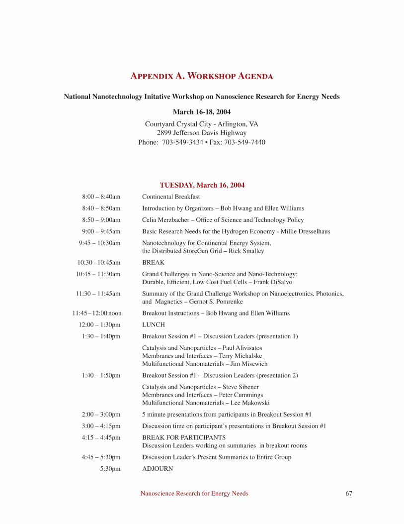
67Nanoscience Research for Energy Needs
TUESDAY, March 16, 2004
8:00 – 8:40am Continental Breakfast
8:40 – 8:50am Introduction by Organizers – Bob Hwang and Ellen Williams
8:50 – 9:00am Celia Merzbacher – Office of Science and Technology Policy
9:00 – 9:45am Basic Research Needs for the Hydrogen Economy - Millie Dresselhaus
9:45 – 10:30am Nanotechnology for Continental Energy System, the Distributed StoreGen Grid – Rick Smalley
10:30 –10:45am BREAK
10:45 – 11:30am Grand Challenges in Nano-Science and Nano-Technology: Durable, Efficient, Low Cost Fuel Cells – Frank DiSalvo
11:30 – 11:45am Summary of the Grand Challenge Workshop on Nanoelectronics, Photonics, and Magnetics – Gernot S. Pomrenke
11:45 – 12:00 noon Breakout Instructions – Bob Hwang and Ellen Williams
12:00 – 1:30pm LUNCH
1:30 – 1:40pm Breakout Session #1 – Discussion Leaders (presentation 1)
Catalysis and Nanoparticles – Paul Alivisatos Membranes and Interfaces – Terry Michalske Multifunctional Nanomaterials – Jim Misewich
1:40 – 1:50pm Breakout Session #1 – Discussion Leaders (presentation 2)
Catalysis and Nanoparticles – Steve Sibener Membranes and Interfaces – Peter Cummings Multifunctional Nanomaterials – Lee Makowski
2:00 – 3:00pm 5 minute presentations from participants in Breakout Session #1
3:00 – 4:15pm Discussion time on participant’s presentations in Breakout Session #1
4:15 – 4:45pm BREAK FOR PARTICIPANTS Discussion Leaders working on summaries in breakout rooms
4:45 – 5:30pm Discussion Leader’s Present Summaries to Entire Group
5:30pm ADJOURN
Appendix A. Workshop Agenda
National Nanotechnology Initative Workshop on Nanoscience Research for Energy Needs
March 16-18, 2004
Courtyard Crystal City - Arlington, VA2899 Jefferson Davis Highway
Phone: 703-549-3434 • Fax: 703-549-7440

Nanoscience Research for Energy Needs68
Appendix A. Workshop Agenda
WEDNESDAY, March 17, 2004
7:45 – 8:30am Continental Breakfast
8:30 – 9:15am Theory and Modeling in Nanoscience – Peter Cummings
9:15 – 10:00am Integrating the Multifunction Necessary for Electrochemical Power into Mesoporous Nanoarchitectures – Debra Rolison
10:00 – 10:15am BREAK
10:15 – 11:00am Carbon Nanotube Electronics and Opto-Electronics – Phaedon Avouris
11:00 – 11:15am Perspective from the NNI Workshop on Materials Grand Challenges – Robert Hull
11:15 – 11:25am Breakout Session #2 – Discussion Leaders (presentation 1)
Catalysis and Nanoparticles – Kristen Fichthorn Membranes and Interfaces – Cherry Murray Multifunctional Nanomaterials – Doug Lowndes
1 1:25 – 11:35am Breakout Session #2 – Discussion Leaders ( presentation 2)
Catalysis and Nanoparticles – Bruce Gates Membranes and Interfaces – Jim DeYoreo Multifunctional Nanomaterials – Arun Majumdar
11:35 – 12:45pm 5 minute presentations from participants in Breakout Session #2
12:45 – 2:00pm LUNCH
2:00 – 3:30pm Discussion time on participants’ presentations in Breakout Session #2
3:30 – 4:00pm BREAK FOR PARTICIPANTS
Discussion Leaders working on summaries in breakout rooms
4:00 – 4:45pm Discussion Leaders Present Summaries to Entire Group
4:45 – 5:30pm Instructions for Next Day to Discussion Leaders
5:30pm ADJOURN
THURSDAY, March 18, 2004
8:00 – 8:30am Continental Breakfast
8:30 – 9:30am Generate 5–8 pages of material per breakout session. The more material that is written during the breakout sessions, the easier this will be to achieve.
9:30 – 10:30am Give materials to different group for proofreading and corrections/suggestions
10:30 – 11:30am Generate Final Version
11:30 – 12:30pm Organizers, Discussion Leaders, and Government representatives meet to finalize deadlines and time-tables, etc.
12:30 – 1:30pm LUNCH
1:30pm ADJOURN
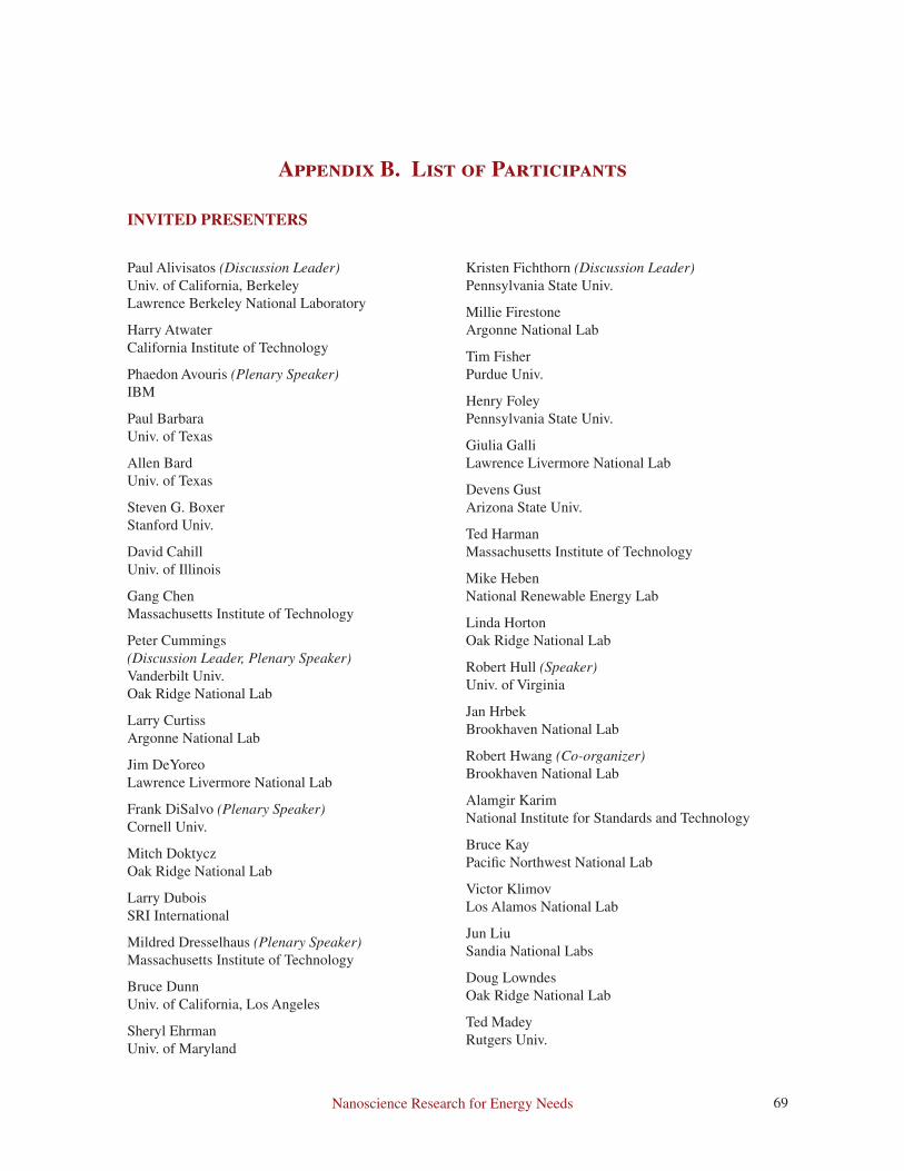
Nanoscience Research for Energy Needs 69
INVITED PRESENTERS
Kristen Fichthorn (Discussion Leader) Pennsylvania State Univ.
Millie Firestone Argonne National Lab
Tim Fisher Purdue Univ.
Henry Foley Pennsylvania State Univ.
Giulia Galli Lawrence Livermore National Lab
Devens Gust Arizona State Univ.
Ted Harman Massachusetts Institute of Technology
Mike Heben National Renewable Energy Lab
Linda Horton Oak Ridge National Lab
Robert Hull (Speaker) Univ. of Virginia
Jan Hrbek Brookhaven National Lab
Robert Hwang (Co-organizer) Brookhaven National Lab
Alamgir Karim National Institute for Standards and Technology
Bruce Kay Pacific Northwest National Lab
Victor Klimov Los Alamos National Lab
Jun Liu Sandia National Labs
Doug Lowndes Oak Ridge National Lab
Ted Madey Rutgers Univ.
Paul Alivisatos (Discussion Leader) Univ. of California, Berkeley Lawrence Berkeley National Laboratory
Harry Atwater California Institute of Technology
Phaedon Avouris (Plenary Speaker) IBM
Paul Barbara Univ. of Texas
Allen Bard Univ. of Texas
Steven G. Boxer Stanford Univ.
David Cahill Univ. of Illinois
Gang Chen Massachusetts Institute of Technology
Peter Cummings (Discussion Leader, Plenary Speaker) Vanderbilt Univ. Oak Ridge National Lab
Larry Curtiss Argonne National Lab
Jim DeYoreo Lawrence Livermore National Lab
Frank DiSalvo (Plenary Speaker) Cornell Univ.
Mitch Doktycz Oak Ridge National Lab
Larry Dubois SRI International
Mildred Dresselhaus (Plenary Speaker) Massachusetts Institute of Technology
Bruce Dunn Univ. of California, Los Angeles
Sheryl Ehrman Univ. of Maryland
Appendix B. List of Participants

Nanoscience Research for Energy Needs
Appendix B. List of Participants
70
Arun Majumdar (Discussion Leader) Univ. of California, Berkeley
Lee Makowski (Discussion Leader) Argonne National Lab
Manos Mavrikakos Univ. of Wisconsin
Celia Merzbacher (Speaker) Office of Science and Technology Policy
Terry Michalske (Discussion Leader) Sandia National Labs
Jim Misewich (Discussion Leader) Brookhaven National Lab
Cherry Murray (Discussion Leader) Lucent Technologies
Marshall Newton Brookhaven National Lab
Steve Overbury Oak Ridge National Lab
Don Parkin Los Alamos National Lab
Gernot Pomrenke (Speaker) Air Force Office of Scientific Research
Michael Postek National Institute for Standards and Technology
Tijana Rajh Argonne National Lab
Art Ramirez Lucent Technologies
Debra Rolison (Plenary Speaker) Naval Research Lab
Andrew Shreve Los Alamos National Lab
Steve Sibener (Discussion Leader) Univ. of Chicago
Jerry Simmons Sandia National Labs
Richard Smalley (Plenary Speaker) Rice Univ.
Randall Snurr Northwestern Univ.
Gabor Somorjai Univ. of California, Berkeley Lawrence Berkeley National Lab
Malcolm Stocks Oak Ridge National Lab
Roland Stumpf Sandia National Labs
Sam Stupp Northwestern Univ.
Eric Stuve Univ. of Washington
John Weeks Univ. of Maryland
Ellen Williams (Co-organizer) Univ. of Maryland
Luping Yu Univ. of Chicago
David Zaziski Nanosys, Inc.
OTHER PARTICIPANTS
Cate Alexander National Nanotechnology Coordination Office
Chagaan Baater Office of Naval Research
Kristen Bennett U.S. Department of Energy Office of Basic Energy Sciences
Altaf Carim U.S. Department of Energy Office of Basic Energy Sciences
Hongda Chen USDA/CSREES
Yok Chen U.S. Department of Energy Office of Basic Energy Sciences
Patricia Dehmer U.S. Department of Energy Office of Basic Energy Sciences
Jonathan Epstein Office of Senator Bingaman

Nanoscience Research for Energy Needs
Appendix B. List of Participants
71
Tim Fitzsimmons U.S. Department of Energy Office of Basic Energy Sciences
Sam Gill National Nanotechnology Coordination Office
Stephen Gould National Nanotechnology Coordination Office
Robert Gottschall U.S. Department of Energy Office of Basic Energy Sciences
Mihal Gross Office of Naval Research
Geoffrey Holdridge National Nanotechnology Coordination Office
Barbara Karn U.S. Environmental Protection Agency
Richard Kelley U.S. Department of Energy Office of Basic Energy Sciences
Harriet Kung U.S. Department of Energy Office of Basic Energy Sciences
Ted Leventhal National Journals Technology Daily
Philip Lippel American Association for the Advancement of Science
John Miller U.S. Department of Energy Office of Basic Energy Sciences
Raul Miranda U.S. Department of Energy Office of Basic Energy Sciences
James Momoh National Science Foundation
Carole Read U.S. Department of Energy Office of Hydrogen Fuel Cells
Nora Savage U.S. Environmental Protection Agency
Glenn Schrader National Science Foundation
Richard Smith National Science Foundation
Walter Stevens U.S. Department of Energy Office of Basic Energy Sciences
Fred Tathwell U.S. Department of Energy Office of Basic Energy Sciences
Clayton Teague National Nanotechnology Coordination Office
Brian Valentine U.S. Department of Energy Office of Energy Efficiency and Renewable Energy
Sharlene Weatherwax U.S. Department of Energy Office of Basic Energy Sciences
Phyllis Yoshida U.S. Department of Energy Freedom CAR Partnership
Jane Zhu U.S. Department of Energy Office of Basic Energy Sciences

things Manmade
Courtesy Office of Basic Energy Sciences, Office of Science, U.S. Department of Energy
things Natural
the Scale ofThings....
&Nanometers
More
things Manmade
Courtesy Office of Basic Energy Sciences, Office of Science, U.S. Department of Energy

National Science and Technology Council
Committee on Technology
Subcommittee on Nanoscale Science, Engineering, and Technology
National Nanotechnology Coordination Office
4201 Wilson Blvd.Stafford II, Rm. 405Arlington, VA 22230
703-292-8626 phone
703-292-9312 fax
www.nano.gov
NNCO_cov.qxd 6/11/04 3:57 PM Page 1


![patriotic hygiene 2013 Cosponsored by UNC's - [email protected]](https://static.fdocuments.net/doc/165x107/620495b54b1be21e4726f6d2/patriotic-hygiene-2013-cosponsored-by-uncs-emailprotected.jpg)

