
ABACUS—Introduction to Semiconductor Devices
14
ABACUS—INTRODUCTION TO SEMICONDUCTOR DEVICES ABACUS—Introduction to Semiconductor Devices When we hear the term semiconductor device, we may think first of the transistors in PCs or video game consoles, but transistors are the basic component in all of the electronic devices we use in our daily lives. Electronic systems are built from such components as transistors, capacitors, wires, light-emitting diodes and semiconductor lasers. These components are typically integrated into a single chip made of a semiconductor material. Almost every college or university department of Electrical Engineering offers instruction in the fundamental concepts of semiconductor devices. These concepts typically include lattices, crystal structure, bandstructure, band models, carrier distributions, drift, diffusion, pn junctions, solar cells, light-emitting diodes, bipolar junction transistors (BJT), metal-oxide semiconductor capacitors (MOS-caps), and multi-acronym-device field-effect transistors (mad-FETs). Advanced courses go more deeply into semiconductor theory, device physics, fabrication processes, as well as advanced and special purpose devices, such as heterostructure devices, power devices, and optoelectronic devices. This nanoHUB “topic page” provides an easy access to selected nanoHUB educational 1 / 14
Transcript of ABACUS—Introduction to Semiconductor Devices

ABACUS—INTRODUCTION TO SEMICONDUCTOR DEVICES
ABACUS—Introduction to Semiconductor Devices
When we hear the term semiconductor device, we may think first of the transistors in PCs orvideo game consoles, but transistors are the basic component in all of the electronic devices weuse in our daily lives. Electronic systems are built from such components as transistors,capacitors, wires, light-emitting diodes and semiconductor lasers. These components aretypically integrated into a single chip made of a semiconductor material.
Almost every college or university department of Electrical Engineering offers instruction in thefundamental concepts of semiconductor devices. These concepts typically include lattices,crystal structure, bandstructure, band models, carrier distributions, drift, diffusion, pn junctions,solar cells, light-emitting diodes, bipolar junction transistors (BJT), metal-oxide semiconductorcapacitors (MOS-caps), and multi-acronym-device field-effect transistors (mad-FETs).
Advanced courses go more deeply into semiconductor theory, device physics, fabricationprocesses, as well as advanced and special purpose devices, such as heterostructure devices,power devices, and optoelectronic devices.
This nanoHUB “topic page” provides an easy access to selected nanoHUB educational
1 / 14

ABACUS—INTRODUCTION TO SEMICONDUCTOR DEVICES
material on semiconductor devices that is openly accessible.
We invite users to participate in this open source, interactive educational initiative:
Contribute content by uploading it to the nanoHUB. (See “Upload your own content”) onthe nanoHUB mainpage. Provide feedback for the items you use on the nanoHUB through the review system.(Please be explicit and provide constructive feedback.) Let us know when things do not work by filing a ticket through the nanoHUB “Help”feature on every page. If you have suggestions for improvements, submit a wish.
Thank you for using the nanoHUB, and be sure to share your nanoHUB success stories with us.We like to hear from you, and our sponsors need to know that the nanoHUB is having impact.
Crystal Structures, Lattices
Crystal Viewer
The Crystal Viewer in ABACUS enables the interactive visualization different Bravais lattices,crystal planes, and materials (diamond, silicon, indium arsenide, gallium arsenide, graphene,and buckyball).
First time use of the tool is supported by: Crystal Viewer Tool: First-Time User Guide
It is supported by a homework assignment in MS Word and Adobe PDF format.
Exercise: Crystal Lattices
2 / 14

ABACUS—INTRODUCTION TO SEMICONDUCTOR DEVICES
Crystal Viewer Tool Learning Materials – Comprehensive set of learning materials for theCrystal Viewer Tool.
Band Models / Band Structure
Piecewise Constant Potential Barriers Lab
This tool computes the transmission and the reflection coefficient of a five, seven, nine, elevenand 2n-segment piecewise constant potential energy profile. It enables the rapid visualization ofthe formation of band structures in a finite superlattice.
First time use of the tool is supported by: Piece-Wise Constant Potential Barriers Tool: First-Time User Guide
The materials below provide a detailed description of the physics required both to use this toolcorrectly and to interpret the results obtained:
Open Systems Double-Barrier Case Explained
3 / 14

ABACUS—INTRODUCTION TO SEMICONDUCTOR DEVICES
Exercises that illustrate the importance of quantum-mechanical reflections in state-of-the-artdevices and the resonance width dependence upon the geometry in the double-barrier structurethat is integral part of resonant tunneling diodes are given below:
Quantum-Mechanical Reflections Quantum-Mechanical Reflections in Nanodevices Double-Barrier Structure
The following assignments help to illustrate the formation of bands in periodic potentials andhow the width and number of the energy bands changes by varying the geometry of the n-wellpotential:
From one well, to two wells, to five wells, to periodic potentials Bands as a function of the geometry of the n-well potential
One can also use this tool to calculate the transmission coefficient through barriers that areapproximated with Piece-Wise constant segments.
Piece-Wise Constant Potential Barriers Tool Learning Materials – Comprehensive set oflearning materials for the Piece-Wise Constant Potential Barriers Tool.
Periodic Potential Lab
4 / 14

ABACUS—INTRODUCTION TO SEMICONDUCTOR DEVICES
The Periodic Potential Lab in ABACUS solves the time independent Schrödinger Equation in aone-dimentional spatial potential variation. Rectangular, triangular, parabolic (harmonic), andCoulomb potential confinements can be considered. The user can determine energetic andspatial details of the potential profiles, compute the allowed and forbidden bands, plot the bandsin a compact and an expanded zone, and compare the results against a simple effective-massparabolic band. Transmission is also calculated through the well for the given energy range.
Exercises:
Periodic Potentials and Bandstructure: an Exercise
Periodic Potential Lab Learning Materials – Comprehensive set of learning materials for thePeriodic Potential Lab.
Band Structure Lab
The Band Structure Lab in ABACUS enables the study of bulk dispersion relationships ofsilicon, gallium arsenide, and indium arsenide. The users can apply tensile and compressivestrain and observe the variation in the band structure, bandgaps, and effective masses.Advanced users can study band structure effects in ultra-scaled (thin body) quantum wells, andnanowires of different cross sections. Band Structure Lab uses the sp3s*d5 tight-bindingmethod to compute E(k) for bulk, planar, and nanowire semiconductors.
5 / 14

ABACUS—INTRODUCTION TO SEMICONDUCTOR DEVICES
Exercises:
Bulk Band Structure: a Simulation Exercise Computational Electronics HW - Simplified Band Structure Model Exercise: Density of States Function Calculation Can we define unique effective masses in Si nanowires?
Band Structure Lab Learning Materials – Comprehensive set of learning materials for the BandStructure Lab.
Bulk Semiconductors
Carrier Statistics Lab
The Carrier Statistics Lab in ABACUS demonstrates electron and hole-density distributionsbased on the Fermi-Dirac and Maxwell-Boltzmann equations. This tool shows the dependenceof carrier density, density of states and occupation factor on temperature and fermi level. Theuser can choose between doped and undoped semi-conductors. silicon, germanium, andgallium arsenide can be studied as a function of doping or Fermi level, and temperature. TheCarrier Statistics Lab is supported by a homework assignment in which students are asked toexplore the differences between Fermi-Dirac and Maxwell-Boltzmann distributions, computeelectron and hole concentrations, study temperature dependences, and the phenomenon offreeze-out.
First time use of the tool is supported by: Carrier Statistics Lab: First-Time User Guide
Exercises:
Exercise: MATLAB Tool Construction for Degenerate/Nondegenerate Semiconductors
6 / 14

ABACUS—INTRODUCTION TO SEMICONDUCTOR DEVICES
That Includes Partial Ionization of the Dopants Exercise: Dopants and Semiconductor Statistics Hall Effect - Theoretical Exercise
Carrier Statistics Lab Learning Materials – Comprehensive set of learning materials for theCarrier Statistics Lab.
Drift Diffusion Lab
The Drift Diffusion Lab in ABACUS enables users to understand the basic concepts of the driftand diffusion of carriers inside a semiconductor slab using different kinds of experiments.Experiments like shining light onto the semiconductor, applying bias, as well as both processessimultaneously, can be performed. This tool provides important information about carrierdensities, transient and steady state currents, Fermi-levels and electrostatic potentials. It issupported by two related homework assignments #1 and #2 in which students are asked toexplore the concepts of drift, diffusion, quasi Fermi-levels, and the response to light.
Exercises:
Conductivity - Theoretical Exercise
Drift-Diffusion Lab Learning Materials – Comprehensive set of learning materials for the Drift-Diffusion Lab.
PN Junctions
PN Junction Lab
7 / 14

ABACUS—INTRODUCTION TO SEMICONDUCTOR DEVICES
PN-Junction Lab in ABACUS is everything users need to explore and teach the basic conceptsof P-N junction devices. Edit the doping concentrations, change the materials, tweak minority-carrier lifetimes, and modify the ambient temperature. Then, see the effects in the energy banddiagram, carrier densities, net charge distribution, current-voltage (I/V) characteristic, and otherphenomena.
There is a significant set of associated resources available for this tool.
a demo of this tool a Primer on Semiconductor Device Simulation. a Learning Module entitled PN Junction Theory and Modeling that walks studentsthrough the PN-junction theory and let’s them verify concepts through on-linesimulation. Homework assignment on the depletion approximation Homework assignment on the depletion approximation
Exercises:
PN Diode Exercise: Series Resistance Exercise: PIN Diode PN Diode Exercise: Graded Junction Basic operation of a PN diode - Theoretical exercise PN diode - Advanced theoretical exercises Schottky diode - Theoretical exercises
PN Junction Lab Learning Materials – Comprehensive set of learning materials for the PNJunction Lab.
Bipolar Junction Transistors (BJT)
Bipolar Junction Lab
8 / 14

ABACUS—INTRODUCTION TO SEMICONDUCTOR DEVICES
The Bipolar Junction Lab in ABACUS allows Bipolar Junction Transistor (BJT) simulation usinga 2D mesh. It allows users to simulate either the npn- or pnp-type of device. Users can specifythe emitter, base and collector region depths and doping densities. Also the material andminority-carrier lifetimes can be specified by the user. The tool is supported by a homeworkassignment in which students are asked to find the emitter efficiency, the base transport factor,current gains, and the Early voltage. Also, students are requested to provide a qualitativediscussion.
Exercises:
BJT - Simulation Exercise BJT - Theoretical Exercise BJT Operation Description
BJT Lab Learning Materials – Comprehensive set of learning materials for the BJT Lab.
MOS Capacitors
MOScap
9 / 14
ABACUS—INTRODUCTION TO SEMICONDUCTOR DEVICES
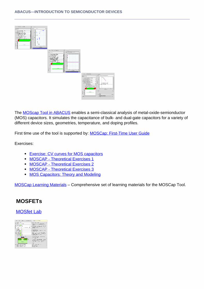
The MOScap Tool in ABACUS enables a semi-classical analysis of metal-oxide-semionductor(MOS) capacitors. It simulates the capacitance of bulk- and dual-gate capacitors for a variety ofdifferent device sizes, geometries, temperature, and doping profiles.
First time use of the tool is supported by: MOSCap: First-Time User Guide
Exercises:
Exercise: CV curves for MOS capacitors MOSCAP - Theoretical Exercises 1 MOSCAP - Theoretical Exercises 2 MOSCAP - Theoretical Exercises 3 MOS Capacitors: Theory and Modeling
MOSCap Learning Materials – Comprehensive set of learning materials for the MOSCap Tool.
MOSFETs
MOSfet Lab
10 / 14

ABACUS—INTRODUCTION TO SEMICONDUCTOR DEVICES
The MOSfet Lab in ABACUS tool enables a semi-classical analysis of current-voltage (I/V)characteristics for bulk and SOI Field-Effect Transistors (FETs) for a variety of different devicesizes, geometries, temperature, and doping profiles.
Exercises:
MOSFET Exercise Exercise: Basic Operation of n-Channel SOI Device MOSFET - Theoretical Exercises MOSFET Operation Description
MOSFet Learning Materials – Comprehensive set of learning materials for the MOSFet Tool.
About ABACUS Constituent Tools
The Assembly of Basic Applications for Coordinated Understanding of Semiconductors(ABACUS) has been put together from individual tools to provide educators and students with aone-stop-shop in semiconductor education. It therefore benefits tremendously from the hardwork that the contributors of the individual tool builders have put into their tools.
As a matter of credit, simulation runs that are performed in the ABACUS tool are also credited tothe individual tools, which help the ranking of the individual tools. We do also count the numberof usages of the individual tools in the ABACUS tool set, to measure the ABACUS impact andpossibly also improve the tool.
In the description above, we do not refer to the individual tools since we want to guide the usersto the composite ABACUS tool. We cite the individual tools here explicitly so they are beinggiven the appropriate credit and on their respective tool pages are being linked to this ABACUStopic page.
Crystal Viewer Lab (New Interactive Front End), Piece-Wise Constant Potential Barriers Tool,(Resource(kronigpenney) failed), Band Structure Lab, Carrier Statistics Lab, Drift-Diffusion Lab, PN Junction Lab, BJT Lab, MOSCap, and MOSFet.
Additional Reading and Tools
Solar Cells
11 / 14

ABACUS—INTRODUCTION TO SEMICONDUCTOR DEVICES
ADEPT
ADEPT is not supported within ABACUS because it is a research-oriented tool that enables thestudy of solar cells for various material systems. A Reference Manual and a ADEPTHeterostructure Tutorial are available. The interface is not a simple point-and-click interface, asfor example the PN junction lab, but simulation commands are entered via a command line.
MOS Capacitors with Quantum Corrections
Schred
Schred is not formally supported in ABACUS. It contains more advancedquantum mechanical concepts and is a nanoHUB contributed tool. It calculates the envelopewavefunctions and the corresponding bound-state energies in a typical metal-oxidesemiconductor (MOS) or semiconductor-oxide-semiconductor (SOS) structure and a typical SOIstructure by solving self-consistently the one-dimensional (1D) Poisson equation and the 1DSchrödinger equation.
Exercises:
Schred: Exercise 1 SCHRED: Exercise 2 Schred: Exercise 3 Quantum Size Effects and the Need for Schred Schred Tutorial Version 2.1
madFETs—more Field Effect Transistors
12 / 14

ABACUS—INTRODUCTION TO SEMICONDUCTOR DEVICES
The Field-Effect Transistor has been proposed and implemented in many physical systems,materials, and geometries. A multitude of acronyms have developed around these concepts.The “Many-Acronym-Device-FET” (madFET) was born. The author of this document was ableto trace an attribute to the acronym madFET from Bill Frensley to Herbert Kroemer.
nanoHUB.org hosts a variety of tools that enable the simulation of field effect transisors for avariety of different geometries in a variety of different levels of approximations. There is a madFETs topics page that provides an overview of many of the nanoHUB.org madFET tools.
Technology Computer Aided Design—TCAD
13 / 14

ABACUS—INTRODUCTION TO SEMICONDUCTOR DEVICES
Once students have mastered the basics of semiconductors they may bequite interested in venturing into TCAD. There is a topics page for aTCADlab and associatedsingle aTCADlab tool that assembles various TCAD tools available on the nanoHUB. Process,device, and circuit simulation is represented in aTCADlab.
Powered by TCPDF (www.tcpdf.org)
14 / 14


![Semiconductor Devices [Kanaan Kano]](https://static.fdocuments.net/doc/165x107/55cf931a550346f57b9bb747/semiconductor-devices-kanaan-kano.jpg)


