Ab-Initio Calculation of the Vibrational Influence on Hole ...
4
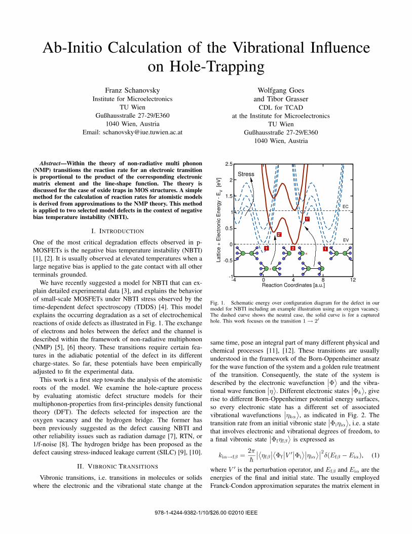
Ab-Initio Calculation of the Vibrational Influence on Hole-Trapping Franz Schanovsky Institute for Microelectronics TU Wien Gußhausstraße 27-29/E360 1040 Wien, Austria Email: [email protected] Wolfgang Goes and Tibor Grasser CDL for TCAD at the Institute for Microelectronics TU Wien Gußhausstraße 27-29/E360 1040 Wien, Austria Abstract—Within the theory of non-radiative multi phonon (NMP) transitions the reaction rate for an electronic transition is proportional to the product of the corresponding electronic matrix element and the line-shape function. The theory is discussed for the case of oxide traps in MOS structures. A simple method for the calculation of reaction rates for atomistic models is derived from approximations to the NMP theory. This method is applied to two selected model defects in the context of negative bias temperature instability (NBTI). I. I NTRODUCTION One of the most critical degradation effects observed in p- MOSFETs is the negative bias temperature instability (NBTI) [1], [2]. It is usually observed at elevated temperatures when a large negative bias is applied to the gate contact with all other terminals grounded. We have recently suggested a model for NBTI that can ex- plain detailed experimental data [3], and explains the behavior of small-scale MOSFETs under NBTI stress observed by the time-dependent defect spectroscopy (TDDS) [4]. This model explains the occurring degradation as a set of electrochemical reactions of oxide defects as illustrated in Fig. 1. The exchange of electrons and holes between the defect and the channel is described within the framework of non-radiative multiphonon (NMP) [5], [6] theory. These transitions require certain fea- tures in the adiabatic potential of the defect in its different charge-states. So far, these potentials have been empirically adjusted to fit the experimental data. This work is a first step towards the analysis of the atomistic roots of the model. We examine the hole-capture process by evaluating atomistic defect structure models for their multiphonon-properties from first-principles density functional theory (DFT). The defects selected for inspection are the oxygen vacancy and the hydrogen bridge. The former has been previously suggested as the defect causing NBTI and other reliability issues such as radiation damage [7], RTN, or 1/f-noise [8]. The hydrogen bridge has been proposed as the defect causing stress-induced leakage current (SILC) [9], [10]. II. VIBRONIC TRANSITIONS Vibronic transitions, i.e. transitions in molecules or solids where the electronic and the vibrational state change at the -4 0 4 8 12 Reaction Coordinates [a.u.] -1 -0.5 0 0.5 1 1.5 2 2.5 Lattice + Electronic Energy - E V [eV] 1 2’ 2 1 Stress EV EC 1’ + + Fig. 1. Schematic energy over configuration diagram for the defect in our model for NBTI including an example illustration using an oxygen vacancy. The dashed curve shows the neutral case, the solid curve is for a captured hole. This work focuses on the transition 1 → 2 0 same time, pose an integral part of many different physical and chemical processes [11], [12]. These transitions are usually understood in the framework of the Born-Oppenheimer ansatz for the wave function of the system and a golden rule treatment of the transition. Consequently, the state of the system is described by the electronic wavefunction Φ and the vibra- tional wave function η . Different electronic states Φ k , give rise to different Born-Oppenheimer potential energy surfaces, so every electronic state has a different set of associated vibrational wavefunctions η kα , as indicated in Fig. 2. The transition rate from an initial vibronic state Φ i η iα , i.e. a state that involves electronic and vibrational degrees of freedom, to a final vibronic state Φ f η f β is expressed as k iα→f β = 2π ¯ h η f β Φ f V 0 Φ i η iα 2 δ(E f β - E iα ), (1) where V 0 is the perturbation operator, and E f β and E iα are the energies of the final and initial state. The usually employed Franck-Condon approximation separates the matrix element in 978-1-4244-9382-1/10/$26.00 ©2010 IEEE
Transcript of Ab-Initio Calculation of the Vibrational Influence on Hole ...
Ab-Initio Calculation of the Vibrational Influenceon Hole-Trapping
Franz SchanovskyInstitute for Microelectronics
TU WienGußhausstraße 27-29/E360
1040 Wien, AustriaEmail: [email protected]
Wolfgang Goesand Tibor Grasser
CDL for TCADat the Institute for Microelectronics
TU WienGußhausstraße 27-29/E360
1040 Wien, Austria
Abstract—Within the theory of non-radiative multi phonon(NMP) transitions the reaction rate for an electronic transitionis proportional to the product of the corresponding electronicmatrix element and the line-shape function. The theory isdiscussed for the case of oxide traps in MOS structures. A simplemethod for the calculation of reaction rates for atomistic modelsis derived from approximations to the NMP theory. This methodis applied to two selected model defects in the context of negativebias temperature instability (NBTI).
I. INTRODUCTION
One of the most critical degradation effects observed in p-MOSFETs is the negative bias temperature instability (NBTI)[1], [2]. It is usually observed at elevated temperatures when alarge negative bias is applied to the gate contact with all otherterminals grounded.
We have recently suggested a model for NBTI that can ex-plain detailed experimental data [3], and explains the behaviorof small-scale MOSFETs under NBTI stress observed by thetime-dependent defect spectroscopy (TDDS) [4]. This modelexplains the occurring degradation as a set of electrochemicalreactions of oxide defects as illustrated in Fig. 1. The exchangeof electrons and holes between the defect and the channel isdescribed within the framework of non-radiative multiphonon(NMP) [5], [6] theory. These transitions require certain fea-tures in the adiabatic potential of the defect in its differentcharge-states. So far, these potentials have been empiricallyadjusted to fit the experimental data.
This work is a first step towards the analysis of the atomisticroots of the model. We examine the hole-capture processby evaluating atomistic defect structure models for theirmultiphonon-properties from first-principles density functionaltheory (DFT). The defects selected for inspection are theoxygen vacancy and the hydrogen bridge. The former hasbeen previously suggested as the defect causing NBTI andother reliability issues such as radiation damage [7], RTN, or1/f-noise [8]. The hydrogen bridge has been proposed as thedefect causing stress-induced leakage current (SILC) [9], [10].
II. VIBRONIC TRANSITIONS
Vibronic transitions, i.e. transitions in molecules or solidswhere the electronic and the vibrational state change at the
-4 0 4 8 12Reaction Coordinates [a.u.]
-1
-0.5
0
0.5
1
1.5
2
2.5
Lattic
e +
Ele
ctr
onic
Energ
y -
EV [e
V]
1
2’
2 1
Stress
EV
EC
1’
+
+
Fig. 1. Schematic energy over configuration diagram for the defect in ourmodel for NBTI including an example illustration using an oxygen vacancy.The dashed curve shows the neutral case, the solid curve is for a capturedhole. This work focuses on the transition 1→ 2′
same time, pose an integral part of many different physical andchemical processes [11], [12]. These transitions are usuallyunderstood in the framework of the Born-Oppenheimer ansatzfor the wave function of the system and a golden rule treatmentof the transition. Consequently, the state of the system isdescribed by the electronic wavefunction
∣∣Φ⟩ and the vibra-tional wave function
∣∣η⟩. Different electronic states∣∣Φk⟩, give
rise to different Born-Oppenheimer potential energy surfaces,so every electronic state has a different set of associatedvibrational wavefunctions
∣∣ηkα⟩, as indicated in Fig. 2. Thetransition rate from an initial vibronic state
∣∣Φiηiα⟩, i.e. a state
that involves electronic and vibrational degrees of freedom, toa final vibronic state
∣∣Φfηfβ⟩
is expressed as
kiα→fβ =2πh
∣∣⟨ηfβ∣∣⟨Φf
∣∣V ′∣∣Φi
⟩∣∣ηiα⟩∣∣2δ(Efβ − Eiα), (1)
where V ′ is the perturbation operator, and Efβ and Eiα are theenergies of the final and initial state. The usually employedFranck-Condon approximation separates the matrix element in
978-1-4244-9382-1/10/$26.00 ©2010 IEEE

−1
0
1
2
3
4
−1 −0.5 0 0.5 1 1.5 2
E/e
V
Q/Å
Oxygen vacancy
neutralhole captured
η neutralη positive
−1
0
1
2
3
4
−1 −0.5 0 0.5 1 1.5 2
E/e
V
Q/Å
Hydrogen bridge
neutralhole captured
η neutralη positive
Fig. 2. One dimensional potentials and examples of vibrational wavefunctionsfor the oxygen vacancy and the hydrogen bridge as extracted from DFT usingthe method of section IV. The hole energy is set to the silicon valence level.Q is the reaction coordinate. In the high-temperature regime, a transition willtake place at the crossing points of the potentials.
(1) into the electronic matrix element∣∣⟨Φf
∣∣V ′∣∣Φi
⟩∣∣2 and theFranck-Condon overlap factor
∣∣⟨ηfβ∣∣ηiα⟩∣∣2.The total transition rate from
∣∣Φi
⟩to∣∣Φf
⟩is now obtained
by considering all transitions between the associated vibronicstates. Obeying the fact that the vibrational system is underconstant random perturbation that leads to a thermal equilib-rium with the environment, one has to thermally average overall initial vibrational states and sum over all final vibrationalstates. Examples for the thermally weighted overlap factorsare given in Fig. 3. The resulting expression for the electronictransition reads
kif = Aiff (2)
Aif =2πh
∣∣⟨Φf
∣∣V ′∣∣Φi
⟩∣∣2 (3)
f = aveα
∑β
∣∣⟨ηfβ∣∣ηiα⟩∣∣2δ(Efβ − Eiα). (4)
This theory has been initally developed in the context ofoptical spectroscopy [13]. There the quantity f describesthe broadening of absorption peaks and is called line shapefunction. Usually, a change in the electronic state of a systemrequires a number of vibrational quanta to be absorbed oremitted, which is why these transitions are called multi-phonontransitions.
III. CAPTURE AND RELEASE AT DEFECT SITES
The multi-phonon theory has been used for the descriptionof non-radiative capture and release of charge carriers atdefect sites in semiconductors and at oxide-semiconductorinterfaces [5], [6], [14], [15]. For oxide traps, one has to
Oxygen vacancy
0 5 10 15 20
Inital state
0
20
40
60
80
100
120
Fin
al sta
te
Hydrogen bridge
0 5 10 15 20
Inital state
0
20
40
60
80
100
120
Fin
al sta
te
1e−10
1e−09
1e−08
1e−07
1e−06
1e−05
0.0001
0.001
0.01
0.1
Fig. 3. Thermally weighted overlap factors as extracted from our calculations.The lower spring constant of the hydrogen bridge allows for more initial statesto have non-negligible occupation probability.
consider the whole system including the vibrational states ofthe defect, as well as the electrons in the gate, the defectand the semiconductor. The defect is assumed to have onerelevant state to be occupied by an electron. In the limit of non-interacting electrons, the hamiltonian of this system is writtenas [5]
H = Ednd +∑k
Eknk + VeN (Q)nd + HN(Q), (5)
where the ni are the number operators for the electronicstates, k runs over all single-electron states in the gate and thesemiconductor, VeN is the binding potential of the electron,and HN is the vibrational hamiltonian. The vector Q inprinciple contains the coordinates of all atoms in the systembut can be usually reduced to the atoms in the direct vincinityof the defect.
During a hole capture transition, the electron residing in thesingle electron state
∣∣φd
⟩is transferred to the state
∣∣φj⟩, whichwas previously unoccupied. The electronic matrix element forthis transition is defined by the matrix element
∣∣⟨φd
∣∣V ′∣∣φj⟩∣∣2of the single electron wave functions. The perturbation oper-ator for non-radiative processes is found in the non-adiabaticoff-diagonal elements of the Born-Oppenheimer hamiltonian[11], [12].
The vibrational wavefunctions and energies for the initialand final state are obtained from
(Ed +∑k
nkEk + VeN + HN)∣∣ηiα⟩ = Eiα
∣∣ηiα⟩ and
(∑k
nkEk + Ej + HN)∣∣ηfβ⟩ = Efβ
∣∣ηfβ⟩. (6)

The energies and vibrational wavefunctions can now be usedto calculate the line-shape function f according to (4). Ed
and Ej influence the energy eigenvalues, but do not changethe functional form of the vibrational wave functions. Theycan thus be removed from the eigensystem and reinserted inthe line shape function expression to give
f(Ej) = aveα
∑β
∣∣⟨ηfβ∣∣ηiα⟩∣∣2δ(Efβ − Eiα + Ej − Ed). (7)
Consequently, the line shape function for non-radiative holecapture is a function of the hole energy. It is calculated fromthe potential energy surfaces of the defect in its differentelectronic states which can be obtained from methods ofquantum chemistry.
IV. THE CALCULATION OF HOLE CAPTURE RATES FORATOMISTIC BULK DEFECT MODELS
Density functional theory (DFT) is a popular method for theatomistic modeling of point defects in materials. The usuallyemployed models are periodic supercell structures. By settingthe number of electrons in the system, different charge statesof the defect structure can be studied. The evaluation of (2)requires to calculate both Aif and f(E), as explained in theprevious section.Aif cannot be obtained using the described models, as both
the perturbation operator and the true single-electron states ofthe system are not present in a DFT calculation. Thus, theyhave to be estimated from a device simulation [6], [15]. Areasonable estimate is obtained from∣∣⟨φd
∣∣V ′∣∣φj⟩∣∣2 ∝ ∣∣⟨xd∣∣φj⟩∣∣2, (8)
where xd is the location of the defect. This turns the evaluationof the matrix element into a tunneling expression that can beeasily implemented into a device simulation [3], [4].
The calculation of the line shape function from DFT is prin-cipally possible. However, approximations have to be made toreduce the complexity of the problem. To make the extractionas simple as possible, we apply the harmonic approximation tothe potential energy surface and assume single-mode coupling,i.e.
HN(Q) = − h2
2M∂2
∂Q2+Mω2
i
2Q2, and (9)
VeN(Q) =M(ω2
f − ω2i )
2Q2 +Mω2
f Qs
(Qs
2−Q
)+ Es,
(10)
where M is the modal mass. The neutral and the positive stateof the defect are now represented by two one dimensionalharmonic oscillators with the frequencies ωi and ωf displacedby Qs and Es. The overlap integral becomes⟨
ηfβ∣∣ηiα⟩ =
⟨ωf , β
∣∣ωi, α⟩, (11)
where∣∣ω, i⟩ is the i-th eigenvector of the harmonic oscillator
of frequency ω. For the evaluation of this integral a numberof different analytical expressions habe been published inliterature. However, most of them are difficult to evaluate
Fig. 4. The alpha-quartz supercell used in this work. The wave functionsare expanded in a plane-wave basis-set up to 800 eV. The core electrons arerepresented using the PAW method.
for large quantum numbers, so we obtained the overlapsby numeric integration of the analytic harmonic oscillatorwavefunctions.
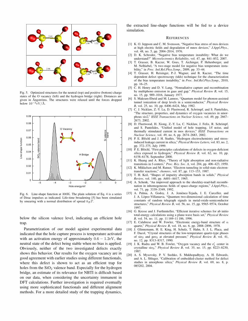
To obtain the required parameters from DFT, the defect totalenergy has been obtained for the neutral and the positive stateof the defect in the neutral and positive optimum configuration(see Fig. 5). From these energies and the assumption ofsingle-mode coupling, all parameters can be obtained in astraight forward way. For the calculations in the present work,the electronic structure is described with density functionaltheory (DFT) using the PBE functional. The calculations havebeen performed using the Vienna ab initio simulation program(VASP) [16].
The host lattice is an orthorhombic alpha-quartz supercellstructure [10], [17], [18] containing 72 atoms. Alpha-quartzwas chosen because it is a well studied reference system foramorphous silica [10], [19], [20]. The determination of defectenergies relative to the silicon bands follows the method ofBlochl [10], where the DFT-energies of the silicon bands aredetermined by fixing the (+/−)-transition level of hydrogento 0.2 eV above the silicon midgap.
V. RESULTS AND CONCLUSION
The extracted potential energy surfaces for the oxygenvacancy and the hydrogen bridge are shown in Fig. 2, thecalculated line-shape functions are shown in Fig. 6. For theoxygen vacancy, the calculation predicts a peak capture crosssection approximately 1eV above the SiO2 valence bandand a thermal activation barrier of approximately 2.8eV forholes at the silicon valence level when no bias is applied.A considerably different behavior is found for the hydrogenbridge, where the positive state of the defect is predicted to bemore stable than the neutral state with a very small activationbarrier. The capture cross section is largest approximately 1eV
2.44
1.98 1.52
2.96
1.64 1.69
Fig. 5. Optimized structures for the neutral (top) and positive (bottom) chargestates of the O vacancy (left) and the hydrogen bridge (right). Distances aregiven in Angstroms. The structures were relaxed until the forces droppedbelow 10−2eV/A.
0
0.01
0.02
0.03
0.04
0.05
0.06
0.07
0.08
0.09
−5 −4 −3 −2 −1 0
Lin
e s
hape function
Hole energy/eV
Si vale
nce
ba
nd
SiO
2 v
ale
nce b
and
O Vacancy
H Bridge
Fig. 6. Line-shape function at 300K. The plain solution of Eq. 4 is a seriesof Dirac impulses as indicated. Life-time broadening [5] has been simulatedby smearing with a normal distribution of spread kBT .
below the silicon valence level, indicating an efficient holetrap.
Parametrization of our model against experimental dataindicated that the hole capture process is temperature activatedwith an activation energy of approximately 0.6 − 1.2eV, theneutral state of the defect being stable when no bias is applied.Obviously, neither of the two investigated defects exactlyshows this behavior. Our results for the oxygen vacancy are ingood agreement with earlier studies using different functionals,where this defect is shown to act as an efficient trap forholes from the SiO2 valence band. Especially for the hydrogenbridge, an estimate of its relevance for NBTI is difficult basedon our data, when considering the uncertainty immanent inDFT calculations. Further investigation is required eventuallyusing more sophisticated functionals and different alignmentmethods. For a more detailed study of the trapping dynamics,
the extracted line-shape functions will be fed to a devicesimulation.
REFERENCES
[1] K. O. Jeppson and C. M. Svensson, “Negative bias stress of mos devicesat high electric fields and degradation of mnos devices,” J.Appl.Phys.,vol. 48, no. 5, pp. 2004–2014, 1976.
[2] D. K. Schroder, “Negative bias temperature instability: What do weunderstand?” Microelectronics Reliability, vol. 47, pp. 841–852, 2007.
[3] T. Grasser, B. Kaczer, W. Goes, T. Aichinger, P. Hehenberger, andM. Nelhiebel, “A two-stage model for negative bias temperature insta-bility,” in Proc. Intl.Rel.Phys.Symp., 2009, pp. 33–44.
[4] T. Grasser, H. Reisinger, P.-J. Wagner, and B. Kaczer, “The timedependent defect spectroscopy (tdds) technique for the characterizationof the bias temperature instability,” in Proc. Intl.Rel.Phys.Symp., 2010,pp. 16–25.
[5] C. H. Henry and D. V. Lang, “Nonradiative capture and recombinationby multiphono emission in gaas and gap,” Physical Review B, vol. 15,no. 15, pp. 989–1016, January 1977.
[6] S. Makram-Ebeid and M. Lannoo, “Quantum model for phonon-assistedtunnel ionization of deep levels in a semiconductor,” Physical ReviewB, vol. 25, no. 10, pp. 6406–6424, May 1982.
[7] C. J. Nicklaw, Z.-Y. Lu, D. Fleetwood, R. Schrimpf, and S. Pantelides,“The structure, properties, and dynamics of oxygen vacancies in amor-phous sio2,” IEEE Transactions on Nuclear Science, vol. 49, pp. 2667–2673, 2002.
[8] D. Fleetwood, H. Xiong, Z.-Y. Lu, C. Nicklaw, J. Felix, R. Schrimpf,and S. Pantelides, “Unified model of hole trapping, 1/f noise, andthermally stimulated current in mos devices,” IEEE Transactions onNuclear Science, vol. 49, no. 6, pp. 2674–2683, 2002.
[9] P. E. Blochl and J. H. Stathis, “Hydrogen electrochemistry and stress-induced leakage current in silica,” Physical Review Letters, vol. 83, no. 2,pp. 372–375, July 1999.
[10] P. E. Blochl, “First-principles calculations of defects in oxygen-deficientsilica exposed to hydrogen,” Physical Review B, vol. 62, no. 10, pp.6158–6178, September 2000.
[11] K. Huang and A. Rhys, “Theory of light absorption and non-radiativetransitions in f-centers,” Proc. Roy. Soc. A, vol. 204, pp. 406–423, 1950.
[12] K. Mikkelsen and M. Ratner, “Electron tunneling in solid-state electron-transfer reactions,” chemrev, vol. 87, pp. 113–153, 1987.
[13] T. H. Keil, “Shapes of impurity absorption bands in solids,” PhysicalReview, vol. 140, pp. A601–A617, 1965.
[14] A. Schenk, “An improved approach to the shockley-read-hall recombi-nation in inhomogeneous fields of space-charge regions,” J.Appl.Phys.,vol. 71, pp. 3339–3349, 1992.
[15] A. Palma, A. Godoy, J. A. Jemenez-Tejada, J. E. Carceller, andJ. A. Lopez-Villanueva, “Quantum two-dimensional calculation of timeconstants of random telegraph signals in metal-oxide-semiconductorstructures,” Physical Review B, vol. 56, no. 15, pp. 9565–9574, October1997.
[16] G. Kresse and J. Furthmueller, “Efficient iterative schemes for ab initiototal-energy calculations using a plane-wave basis set,” Physical ReviewB, vol. 54, no. 11, pp. 11 169–11 186, 1996.
[17] E. Calabrese and W. Fowler, “Electronic energy-band structure of αquartz,” Physical Review B, vol. 18, no. 6, pp. 2888–2896, 1978.
[18] J. Glinnemann, H. E. King, H. Schulz, T. Hahn, S. J. L. Placa, andF. Dacol, “Crystal structures of the low-temperature quartz-type phasesof sio2 and geo2 at elevated pressure,” Physical Review B, vol. 41,no. 12, pp. 8313–8317, 1990.
[19] J. K. Rudra and W. B. Fowler, “Oxygen vacancy and the e′1 center incrystalline sio2,” Physical Review B, vol. 35, no. 15, pp. 8223–8230,1987.
[20] A. S. Mysovsky, P. V. Sushko, S. Mukhopadhyay, A. H. Edwards,and A. L. Shluger, “Calibration of embedded-cluster method for defectstudies in amorphous silica,” Physical Review B, vol. 69, no. 8, p.085202, 2004.