a2) United States Patent US9,562,939 B2
30
US009562939B2 a2) United States Patent Verhulst et al. US 9,562,939 B2 *Feb. 7, 2017 (0) Patent No.: (45) Date of Patent: (54) SYSTEM AND METHOD FOR IMPEDANCE (52) U.S. Cl MEASUREMENT USING SERIES AND CPC wee GOIR 29/26 (2013.01); GOIR 27/02 SHUNT INJECTION (2013.01); GOIR 27/16 (2013.01) (71) Applicants:Huntington Ingalls, Inc., Newport (58) Field of Classification Search / News, VA (US); Virginia Tech CPC Smee meee n eee eeenee een eenee een eee essences seeeeeeeeeees GOIR 29 26 Intellectual Properties, Inc., (Continued) Blacksburg, VA (US) (56) References Cited (72) Inventors: Jacob Verhulst, Newport News, VA (US); Mohamed Belkhayat, Annandale, U.S. PATENT DOCUMENTS VA (US); Zhiyu Shen, Blacksburg, VA (US); Marko Jaksie, Blacksburg, VA 2012/0007583 AL* 1/2012 Martens ........... GOIR 31/3163 : ali ; 324/76.39 (US); Paolo Mattavelli, Blacksburg, VA 2013/0099800 AL* 4/2013 Francis. vcs GOIR 27/02 (US); Dushan Boroyevich, Blacksburg, 324/650 VA (US) (73) Assignees: Huntington Ingalls Incorporated, OTHER PUBLICATIONS Newport News, VA (US); Virginia ; Tech Intellectual Properties, Inc., Zhiyu Shenet al., Design and Implementation of Three-phase AC Blacksburg, VA (US) Impedance Measurement Unit IMU) with Series and Shunt Injec- tion, 2012 IEEE Applied Power Electronics Conference and Expo- (*) Notice: Subject to any disclaimer, the term of this sition—APEC 2012, pp. 1-8, Feb. 2012. patent is extended or adjusted under 35 (Continued) U.S.C. 154(b) by 793 days. This patent is subject to a terminal dis- Primary Examiner — Sujoy Kundu claimer. Assistant Examiner — Xiuquin Sun (74) Attorney, Agent, or Firm — Hunton & Williams LLP (21) Appl. No.: 13/954,014 ; (57) ABSTRACT (22) Filed: Jul. 30, 2013 A method for impedance measurementin a three-phase AC (65) Prior Publication Data system is provided. The method includes injecting a shunt perturbation signal into the three-phase AC system and US 2014/0032148 Al Jan. 30, 2014 collecting a response to the shunt perturbation signal, and Related U.S. Application Data injecting a series perturbation signal into the three-phase AC . . system and collecting a response to the series perturbation (60) Provisional application No. 61/677,256, filed on Jul. signal. The response to the shunt perturbation signal and the 30, 2012, provisional application No. 61/677,271, responseto the series perturbation signal are then transferred filed on Jul. 30, 2012. from abc coordinate to dq coordinates. At least one imped- ance of the three-phase AC system is calculated based on the (51) Int. Cl. responseto the shunt perturbation signal and the response to GOIR 25/00 (2006.01) the series perturbation signal. GOIR 29/26 (2006.01) (Continued) 12 Claims, 19 Drawing Sheets 700 720 730 _Sarhas Shunt BM DATA ACQUISIT IGM, PROCESSING, AND USER INTERFACE "740
Transcript of a2) United States Patent US9,562,939 B2

US009562939B2
a2) United States PatentVerhulst et al.
US 9,562,939 B2*Feb. 7, 2017
(0) Patent No.:
(45) Date of Patent:
(54) SYSTEM AND METHOD FOR IMPEDANCE (52) U.S. Cl
MEASUREMENTUSING SERIES AND CPC wee GOIR 29/26 (2013.01); GOIR 27/02
SHUNT INJECTION (2013.01); GOIR 27/16 (2013.01)
(71) Applicants:Huntington Ingalls, Inc., Newport (58) Field of Classification Search /News, VA (US); Virginia Tech CPC Smee meee n eee eeenee een eenee een eee essences seeeeeeeeeees GOIR 29 26
Intellectual Properties, Inc., (Continued)Blacksburg, VA (US)
(56) References Cited(72) Inventors: Jacob Verhulst, Newport News, VA
(US); Mohamed Belkhayat, Annandale, U.S. PATENT DOCUMENTSVA (US); Zhiyu Shen, Blacksburg, VA(US); Marko Jaksie, Blacksburg, VA 2012/0007583 AL* 1/2012 Martens ........... GOIR 31/3163
: ali ; 324/76.39(US); Paolo Mattavelli, Blacksburg, VA 2013/0099800 AL* 4/2013 Francis. vcs GOIR 27/02(US); Dushan Boroyevich, Blacksburg, 324/650VA (US)
(73) Assignees: Huntington Ingalls Incorporated, OTHER PUBLICATIONSNewport News, VA (US); Virginia ;Tech Intellectual Properties, Inc., Zhiyu Shenet al., Design and Implementation of Three-phase AC
Blacksburg, VA (US) Impedance Measurement Unit IMU) with Series and Shunt Injec-
tion, 2012 IEEE Applied Power Electronics Conference and Expo-
(*) Notice: Subject to any disclaimer, the term ofthis sition—APEC 2012, pp. 1-8, Feb. 2012.
patent is extended or adjusted under 35 (Continued)U.S.C. 154(b) by 793 days.
This patent is subject to a terminal dis- Primary Examiner — Sujoy Kunduclaimer. Assistant Examiner — Xiuquin Sun
(74) Attorney, Agent, or Firm — Hunton & Williams LLP(21) Appl. No.: 13/954,014
; (57) ABSTRACT
(22) Filed: Jul. 30, 2013 A method for impedance measurementin a three-phase AC
(65) Prior Publication Data system is provided. The method includes injecting a shuntperturbation signal into the three-phase AC system and
US 2014/0032148 Al Jan. 30, 2014 collecting a response to the shunt perturbation signal, andRelated U.S. Application Data injecting a series perturbation signal into the three-phase AC
. . system and collecting a response to the series perturbation(60) Provisional application No. 61/677,256, filed on Jul. signal. The response to the shunt perturbation signal and the
30, 2012, provisional application No. 61/677,271, responseto the series perturbation signal are then transferred
filed on Jul. 30, 2012. from abc coordinate to dq coordinates. At least one imped-
ance of the three-phaseAC system is calculated based on the
(51) Int. Cl. responseto the shunt perturbation signal and the response toGOIR 25/00 (2006.01) the series perturbation signal.GOIR 29/26 (2006.01)
(Continued) 12 Claims, 19 Drawing Sheets
700
720 730
_Sarhas Shunt
BM
DATA ACQUISIT IGM,PROCESSING, ANDUSER INTERFACE
"740

US 9,562,939 B2
Page 2
(51) Int. Cl.GOIR 27/02 (2006.01)
GOIR 27/16 (2006.01)
(58) Field of Classification SearchUSPC oiecee cesseereeseeseesescnesensecsesenesaeats 702/65
See application file for complete search history.
(56) References Cited
OTHER PUBLICATIONS
Zhiyu Shenet al., Three-phaseAC System Impedance Measurement
Unit IMU) using Chirp Signal Injection, 2012 TEEE Applied Power
Electronics Conference and Exposition—APEC 2012,pp. 1-9, Feb.
2012.Gerald Francis, “An Algorithm and System for Measuring Imped-
ance in D-Q Coordinates”, Jan. 25, 2010, pp. 1-163.
Gerald Francis et al., “An Algorithm and Implementation System
for Measuring Impedance in the D-Q Domain”, IEEE, 2011, pp.
3221-3228.
* cited by examiner
US 9,562,939 B2Sheet 1 of 19Feb. 7, 2017U.S. Patent
("FY
eouepedul|
peo7
Lb‘Sila
an
(yt
@PayCol
Q)Pa
+ys
yh
(51
OT
PPS
(SZ
souepeduy
aoinos
G)
bs.iNy
aresG)>
+

U.S. Patent Feb.7, 2017 Sheet 2 of 19 US 9,562,939 B2
Day(s)
yl a
= ssN
S .
wl ©LL
>2=Bw
Ie
1
{<————__---------F
A
>“se
SS+ a
eS
Tdg

U.S. Patent Feb.7, 2017 Sheet 3 of 19 US 9,562,939 B2
300
305
m Inject Perturbation “
i 310
Collect Response(s) to vePerturbation
Y 315we~ ~ae af
Yes~~ Additional
“~..Perturbation(s)?_
No
’ 320
| Transfer Voltage and Current| Response(s) From abc (“Coordinates to dg Coordinates |
Y 325Apply Discrete Fourier 46
Transform (DFT)
j 330
Calculate Impedance(s) |~~
FIG. 3

US 9,562,939 B2Sheet 4 of 19Feb. 7, 2017U.S. Patent
(s)PTZ
aouepeduly
peo7
bOld
ay’ly"SA
Can
+tA)
+<PT=(PT
\Y
(1) "S1—>
G)PI4(PSA
(Pd
++
-+
—rireyty
oi
007
(s)2PS7
souepedul]
gounos
(i)peas,{
(Py

U.S. Patent Feb. 7, 2017 Sheet 5 of 19 US 9,562,939 B2
ys
ts)
FIG.
5a

US 9,562,939 B2Sheet 6 of 19Feb. 7, 2017U.S. Patent
QS
‘Sld
—=9dA

US 9,562,939 B2Sheet 7 of 19Feb. 7, 2017U.S. Patent
eg*
—_—_—_—_—_—'
||
@OUSLOJOIi6
aBeYOA9G
OPA
¥by
as
poe
joyesuadwoo
P|
aBeyonog
PtPy
|Joyesuaduico
|ry
QOUaIajouwe
OBAonionsu
ral
tneBPnnn
:yUuadino
—,
°ae
eoueqinyed
jOUUBLOp
NeneyauueUdb
SQOKQnnn
nnn
AtDpee
YW)JOW@AUOD
Ang
oa
|JoyesuedWic
gouasalal
—_
Pyag
euueusb
aourqunwed|
jouueY
youueyob
200

US 9,562,939 B2Sheet 8 of 19Feb. 7, 2017U.S. Patent
99
‘Sid
BOUSIOJOL
QOUBIBIOI
aoueqinwed
souequnyied
jauueyob
jauueByop
byU
UY
PyY
v.
||
||
|vv
Fenpelo
ee
*ga
epnyubeyy
J9USAUODa
JyAhr
°q
{‘SSOa
<i»
=f.
|
sJoyesuedwo0o
ee
abeyonoq
PA
moKYi+
BOUSIOIOI
abeyoaoq
9009

US 9,562,939 B2Sheet 9 of 19Feb. 7, 2017U.S. Patent
SOvVANZLINENaSN
Ov.
|ony‘ONISSS90Nd
‘NOLLISINDOYvivd
uaa
QooOtf

U.S. Patent Feb.7, 2017 Sheet 10 of 19 US 9,562,939 B2
%
/ ,
f! 2sJl DB
fl |/ | !
|
/ |
2
_—_— a mn z
S>
2
«)
i3 ny
bh
|
Lh eS
LAN4\ 3
\ \
\\\
\Qo
N 2 oO © <t N of
(My) 4amod jndjno xeyy

US 9,562,939 B2Sheet 11 of 19Feb. 7, 2017U.S. Patent
&6
‘Old
jeubisSoreuy
»
sesuepusduy|
LMOUYUL)
~~
,a
BORLa}U]
yeubis
a1.
Ja]jOU0D
;SUEO
JYOWMS
JSuUIeUIA6
ywqebigi
a5
me
_S—
<
i
o:
rote
-—
:g
3S|
&o
2S|
3oOo
©g
Oo)=
~a
wae
eo
_—
\‘
‘‘
*ssouepusduyy
‘ae,
eyFP
umouyuy)i
BINS
\;/
\.
/
2006

US 9,562,939 B2Sheet 12 of 19Feb. 7, 2017U.S. Patent
MOAYOR
96
‘Sid
symmouaAxeyixne
pue
SIOUIOJSUB.YUOTR{OSs]
LO
SOSUaS
(SION
2?ISA)
SHNSI19
MOAJUST
uonoafuy
uonEqinyisdg
tunBuroyrpuos
[eusis
Jomndwoy[xd
&SooSa

U.S. Patent Feb.7, 2017 Sheet 13 of 19 US 9,562,939 B2
Eye
Magniue8}
Phase(d
ag)
tae
Frequency (Hz
FIG. 10a
oe
mo
gewow, 2Fea)os 2ome
se .= 40ossPees .
=
Sow» Lea et ae 3 2 3
12 1G He
mo
OSS
Ce
me
Phase{deg}
woeSD
bs
any t 2 310 1 10Frequency (Hz)
FIG. 10b

U.S. Patent Feb.7, 2017 Sheet 14 of 19 US 9,562,939 B2
aewm 20
atte
wt
Mang
niti
uedB
de
ann
ED
oS <
ot
we a
t
osos
a4g wD 40 1Frequency {Hz}
FIG. 10c
OO
Magnilue{a6}
x3 4
ig 40 HW
Frequency (Nz)
FIG. 10d

U.S. Patent Feb.7, 2017 Sheet 15 of 19 US 9,562,939 B2
Pm
fo
he
ww
wy>
©
Magnitue(dB)
2
NS
we
OR
rang
490
deg)
Phase
16 10 1 10°Frequency (Hz)
FIG. 11a
Magnitue
(dB)
70D
“408
Phase
(deg)
&
10° 1 4
Frequency (Hz)
FIG. 11b

U.S. Patent Feb.7, 2017 Sheet 16 of 19 US 9,562,939 B2
oOS®oSB.¢D.oS
= os
® 0&® -100ra0]x.a
10° 10° 10° 10°Frequency(Hz)
FIG. 11c
re
&
Magnitue(dB)
er
Co
©
eo ©o ts10 40° 40ak
Oo
ho
Qo
oO
Phase
(deg)
8
4 = open rth10° 10° 40 40
Frequency(Hz)
FIG. 11d

US 9,562,939 B2
ékOld
Sheet 17 of 19Feb. 7, 2017
U.S. Patent
bpps
weeee
a
2yun)
7OF
CpaUsrns
LAA
AY
=
uawaunseayyOOpe
oy
Hugor
aouepeduy|
AOZaA
Cs
AAA
roe
OO
H
\\/
.?
097
AO¢L
VA
60zT

U.S. Patent Feb.7, 2017 Sheet 18 of 19 US 9,562,939 B2
~ 6 i LO EN ag!3 iG ? RP RP aay
o wt
48 $8) VW
Frequency (Hz)
FIG. 13a
MagnitueGB3
e EH} becbbindon
re a#me
& i
aneue
FIG. 13b
U.S. Patent Feb.7, 2017 Sheet 19 of 19 US 9,562,939 B2
Ratavatatalalatataratntarn’
Maonitae(8)
ay any ay
Frequency (Hz)
FIG. 13c
aye
MagnitueiB}
Tid
e
HE}
Phase
tcdeg}
at 1Fraquency (Nz)
FIG. 13d
US 9,562,939 B2
1SYSTEM AND METHOD FOR IMPEDANCE
MEASUREMENTUSING SERIES AND
SHUNT INJECTION
PRIORITY
This application claims the benefit of U.S. ProvisionalApplication No. 61/677,256, filed Jul. 30, 2012, and U.S.
Provisional Application. No. 61/677,721, filed Jul. 30, 2012,both of which are incorporated by reference hereto in their
entirety for any purpose.
TECHNICAL FIELD
The present disclosure relates generally to systems and
methods for impedance measurementand, moreparticularly,to systems and methods for impedance measurement using
series and shunt injection.
BACKGROUND
Theidentification and subsequent measurement of source
and load impedances are useful tools for assessing andevaluating stability of electrical power systems. The imped-
ance of an alternating current (AC)electrical system may bemeasured by injecting a perturbation signal in the direct and
quadrature (dq) reference frame of the system, and measur-ing the voltage and current response to the perturbation.
Conventionally, impedances of a system at AC interfaces
have been extracted in the direct and quadrature (dq) refer-ence frame using only shunt injection. Problems arise in
such conventional impedance measurement methodsbecause the source impedanceis usually much smaller than
the load impedance at AC interfaces. When perturbing the
system using shunt mode, mostof the injected current flowsinto the low impedance source side. The high impedance
load side is not disturbed enough, resulting in a low signal-to-noise ratio (SNR) which is not good for measurement
accuracy. Further, conventional approaches have generallybeen limited to linear loads and are not well-adapted for
non-linear loads.
Therefore, there is a need for a system and methodcapable of realizing improved load-side SNR and overall
impedance measurement accuracy.
SUMMARY OF THE INVENTION
An illustrative aspect of the invention provides a methodof impedance measurement in a three-phase alternating
current (AC) system. The method comprises injecting a
shunt perturbation signal into the three-phase alternatingcurrent AC system and collecting a response to the shunt
perturbation signal. The method also comprises injecting aseries perturbation signal into the three-phase AC system
and collecting a response to the series perturbation signal.The response to the shunt perturbation signal and the
responseto the series perturbation signal are then transferred
from abe coordinate to dq coordinates. The method furthercomprises calculating at least one impedanceof the three-
phase AC system based on the response to the shunt per-turbation signal and the response to the series perturbation
signal.Anotherillustrative aspect of the invention provides a
system for performing impedance measurementin a three-
phase alternating current (AC) system. The system com-prises an injection circuit configured to inject a shunt
perturbation and a series perturbation signal into the three-
10
20
25
30
35
40
45
50
55
60
65
2phase AC system. The system also comprises a collection
circuit configured to collect a response to the shunt pertur-
bation signal and to collect a response to the series pertur-
bation signal. The system further comprises a control unitconfigured to transfer the response to the shunt perturbation
signal and the responseto theseries perturbation signal fromabc coordinate to dq coordinates andto calculate at least one
impedance of the three-phase AC system based on the
response to the first perturbation signal and the response tothe second perturbation signal.
BRIEF DESCRIPTION OF THE DRAWINGS
The accompanying drawings, which are incorporated in
and constitute a part of this disclosure, illustrate aspectsconsistent with the present disclosure and, together with the
description, serve to explain advantages and principles of
the present disclosure. In the drawings:FIG. 1 schematically illustrates an example three-phase
alternating current (AC) system in dq coordinates, consistentwith certain disclosed embodiments;
FIG. 2 schematically illustrates an example representationof a system response to disturbance, consistent with certain
disclosed embodiments;
FIG.3 is an exemplary flow chart illustrating a method ofinjecting one or moreperturbations and determining source
and load impedance values, consistent with certain disclosedembodiments;
FIG. 4 schematically illustrates an example three-phasealternating current (AC) system in dq coordinates, consistent
with certain disclosed embodiments;
FIG. 5a schematically illustrates an example shuntinjec-tion circuit, consistent with certain disclosed embodiments;
FIG. 54 schematically illustrates an example series injec-tion circuit, consistent with certain disclosed embodiments;
FIG.6a is a block diagram illustrating an example control
diagram of a shunt injection circuit, consistent with certaindisclosed embodiments;
FIG.6is a block diagram illustrating an example controldiagram of a series injection circuit, consistent with certain
disclosed embodiments;FIG.7 is a block diagram illustrating an example repre-
sentation of a system using both shunt injection and series
injection, consistent with certain disclosed embodiments;FIG. 8 is a graph illustrating an example maximum
injection power over frequency, consistent with certaindisclosed embodiments;
FIG.9a is a block diagram illustrating an example imped-ance measurement system, consistent with certain disclosed
embodiments;
FIG. 96 illustrates an example impedance measurementsystem, consistent with certain disclosed embodiments;
FIG. 10a graphically illustrates an example output imped-ance of a three-phase power supply, consistent with certain
disclosed embodiments;FIG. 108 graphically illustrates an example output imped-
ance of a three-phase power supply, consistent with certain
disclosed embodiments;FIG. 10c graphically illustrates an example output imped-
ance of a three-phase power supply, consistent with certaindisclosed embodiments;
FIG. 10d graphically illustrates an example output imped-ance of a three-phase power supply, consistent with certain
disclosed embodiments;
FIG. lla graphically illustrates an example extractedimpedanceofa three-phase R-L load, consistent with certain
disclosed embodiments;
US 9,562,939 B2
3FIG. 114 graphically illustrates an example extracted
impedanceofa three-phase R-L load, consistent with certain
disclosed embodiments;
FIG. 11e graphically illustrates an example extractedimpedanceofa three-phase R-L load, consistent with certain
disclosed embodiments;FIG. 11d graphically illustrates an example extracted
impedanceofa three-phase R-L load, consistent with certain
disclosed embodiments;FIG. 12 schematically illustrates an example measure-
ment system including a six-pulse diode rectifier, consistentwith certain disclosed embodiments;
FIG. 13a graphically illustrates an example extractedimpedance of an input impedance of a diode rectifier,
consistent with certain disclosed embodiments;
FIG. 136 graphically illustrates an example extractedimpedance of an input impedance of a diode rectifier,
consistent with certain disclosed embodiments;FIG. 13c graphically illustrates an example extracted
impedance of an input impedance of a diode rectifier,consistent with certain disclosed embodiments; and
FIG. 13d graphically illustrates an example extracted
impedance of an input impedance of a diode rectifier,consistent with certain disclosed embodiments.
DETAILED DESCRIPTION
Embodiments of the systems and methods described
herein enable the extraction of data related to electric powersystem impedances. Stability of an electric power system
can be assessed by frequency domain analysis of the “minor
loop gain” transfer function, which is defined as the Z./Z,impedance ratio, where Z, is the source impedance and Z,
is the load impedanceat interfaces where the source(s) andload(s) are connected. The power system may be energized
(online) and operating at various loading levels ranging from
no-load to full-load. Embodiments of the present inventionmay use series and shunt modes of perturbation injection to
perform impedance measurements at alternating current(AC) power system interfaces.
Moreparticularly, embodiments of the present disclosureuse a series injection mode when measuring the high imped-
ance side (typically the load side in AC systems). Further,
instead of injecting a perturbation current, a voltage pertur-bation is used in series perturbation mode. By using this
provision, most of the injected power flows to the higherimpedanceload side, thereby raising the load side measure-
ment SNRresulting in a more accurate measurement. Thus,by using both series injection mode and shunt injection
mode, overall impedance measurement can be improved.
The following detailed description refers to the accom-panying drawings. Wherever possible, the same reference
numbers will be used throughout the drawings and thefollowing description to refer to the sameor like parts. While
several exemplary embodiments and features are describedherein, modifications, adaptations, and other implementa-
tions are possible, without departing from the spirit and
scope of the disclosure. For example, substitutions, addi-tions or modifications may be made to the components
illustrated in the drawings, and the exemplary methodsdescribed herein may be modified by substituting, reorder-
ing or adding steps to the disclosed methods. Accordingly,the following detailed description is not intended to limit the
disclosure to any specific embodiments or examples.
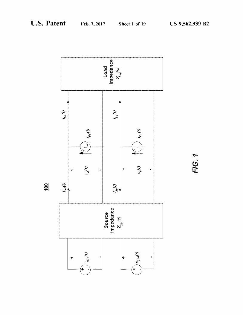
FIG. 1 schematically illustrates an example three-phaseAC system 100 in dq coordinates, consistent with certain
disclosed embodiments. As shown in FIG.1, a three-phase
10
15
20
25
30
35
40
45
50
55
60
65
4balanced and symmetrical system in abe coordinates can bemapped into a stationary system with a constant steady-stateoperating condition by applying the dq transformation. Thatis, by applying the dq transformation, a commonthree-phaseAC system receiving shunt current injections can beexpressed using an equivalent representation, such as therepresentation shown bythe solid parts of system 100 FIG.1.
Generally, a shunt is a device that allows electric currentto pass around anotherpoint in the circuit by creating a lowresistance path. In some embodiments, the shunt device maybe achieved byplacing a resistor, having a knownresistancevalue, in series with the load. The voltage drop across theshunt is proportionalto the current flowing through it, whichcan be calculated because the resistance value is known.
Further, as reflected in FIG. 1, the AC voltages andcurrents in abc coordinates may be transformed into directcurrent (DC) components in dq coordinates. In someembodiments, the voltages and currents collected or sensedat the interface may be transformed into constant values inthe synchronous coordinates at the steady-state. The smallsignal impedance can be obtained by linearizing the systemaround the operating point. In FIG. 1, the dotted linesrepresent a disturbance to the system. As shown in Equation(1), the small-signal interface voltages and currents arerelated by the impedances. The disturbance may be, forexample, a perturbation.
¥a(s) Tsa(s) Equation (1)
| | = Zsui| |Vqls) Tsq(s)
Vals) Tra(s)« = LZiaqls)¥g(s) Trg (s)
where Z.,,(S) is a source impedance matrix;Zzaq(S) 18 a load impedance matrix;¥As) is a d-axis voltage perturbation;¥,(s) is a q-axis voltage perturbation;icAs) is a d-axis source current perturbation;i,,(s) is a q-axis source current perturbation;i,AS) is a d-axis load current perturbation;i,,(s) is a q-axis load current perturbation; ands is the Laplace parameter.
FIG. 2 schematically illustrates an example representation200 of a system response to disturbance, consistent withcertain disclosed embodiments. That is, when a disturbanceis introduced to a system, such as the currents illustrated bythe dashedlines in FIG. 1, the response can be expressed asshown in the example block diagram of FIG. 2. In someembodiments, the disturbance introduced to the system may
be a perturbation, and maybe introducedfor the purpose ofmeasuring a system response. In the example block diagram
of FIG.2, the tildes denote the small signal componentofthevoltages (i.e., ¥) and currents (i.e., 1) of FIG. 1. Stability of
a system, such as the example system of FIG. 2, may beevaluated using the generalized Nyquist stability criterion,
which verify whether the characteristic loci of the return
ratio matrix Z.7,(8)Yzaq(s) encircles the point (-1+0i).The impedances extracted based on the system response
to disturbances, such as the example disturbancesreflectedin FIG. 2, can be represented by 2x2 matrices, such as that
of Equation (2).
Zsaa(s) Zsag(s) | Equation (2)
2say(s) = ea. (8) Zsaq(s)

US 9,562,939 B2
5-continued
Zrad(S) Zags) |
Aug's) =a(8) Zigg(s)
where Zsaq(8) is a source impedance matrix;ZsadS) 1s a dd element of source impedance;Zsaq(S) 18 a dq element of source impedance;ZsqAS) 18 a qd element of source impedance;
Zsqq(S) 18 a qq element of source impedance;Zraq(8) is a load impedance matrix;
ZradS) 1s a dd element of load impedance;Zraq(8) is a dq element of load impedance;
Zzqd8) 1s a qd element of load impedance; and
Zrqq(8) 18 a qq element of load impedance.FIG. 3 presents an exemplary flow chart illustrating a
method 300 of injecting one or more disturbances into apowersystem, and determining source and load impedance
values in response to those disturbances, consistent withcertain disclosed embodiments. As used herein, a distur-
bance introduced into the power system may bea perturba-
tion, such as a series injection signal, a shunt injectionsignal, or any combination of series and shunt injection
signals.In the method 300, a perturbation may be injected into an
electrical power system at 305. The electrical power systemmay be an alternating current (AC)electrical power system.
In some example embodiments, the perturbation may
include one or more shunt injection signals, such as a chirpsignal or a wide-band linear chirp signal. A chirp signalis a
signal in which the frequency increases or decreases withtime. The term chirp or chirp signal is often used inter-
changeably with sweep signal or swept-sine signal. Chirpsignals may include, for example, linear chirp signals,
sinusoidallinear chirp signals, and exponential chirp signals.
For linear chirp signals, the instantaneous frequency, whichis the derivative of the signal phase, may changelinearly as
a function of time. The use of shunt injection signals may bereferred to as shunt injection mode. Equation (3), shown
below, is a time-domain function for a sinusoidal linear chirpsignal, consistent with certain disclosed embodiments.
Equation (3) fi-fo r)x(t) = sin|2rfo + oF
where f, is a start frequency;f, is an end frequency;
T is a duration of the chirp signal; andt is a time.
In the time domain, the instantaneous frequency may bedescribed by Equation (4) below. The instantaneous fre-
quency may be accompanied by additional frequencies,
referred to as harmonics. Generally, a harmonic frequency ofa wave is a component frequency of the signal that is an
integer multiple of the fundamental frequency. For example,if the fundamental frequencyis f, then the harmonics have
frequencies of 2f, 3f, 4f, etc. Harmonics exist as a funda-mental consequence of frequency modulation. Frequency
modulation is the encoding of information in a carrier wave
by varying the instantaneous frequency of the wave.
fi - fo2T
Equation (4) fM= fot t
10
15
25
40
45
50
65
6Additionally and/or alternatively, the perturbation of the
example embodiments may include one or more series
injection signals. The use of series injection signals may be
referred to as a series injection mode. In embodiments, aseries injection mode may be used when measuring the high
impedance side, which is typically the load side in ACsystems. When series injection mode is used, most of the
power flows to the higher impedance load side, therebyraising the load side measurement SNR, which can result in
a more accurate measurement. Unlike a shunt injection
mode, in which a current perturbation is injected into thesystem, in a series injection mode, a voltage perturbation is
injected into the system.Returning to the method 300 of FIG.3, circuit responses
at the AC interfaces may then be collected at 310. Circuitresponses may include Z,, the source impedance, and Z,, the
load impedance. In some embodiments, 7, and Z, may be
measured at interfaces where the source(s) and load(s) areconnected.
A determination as to whether additional perturbations areto be injected may be made at 315. In some embodiments,
only a single perturbation may be used, while in otherembodiments, two perturbations may be used. If the system
is held in a steady-state, more than two perturbations may be
used to improve measurement accuracy. In some embodi-ments, a system for carrying out the method 300 may be
configured to determine whether additional perturbations areto be performed. This determination may be based on system
measurements or by accessing a memory location andretrieving a parameter that defines a number of desired
perturbations. The parameter maybeset, for example, via a
user interface associated with the system. The memorylocation may include any suitable type of memory, such as,
for example, RAM, ROM, programmable read-onlymemory (PROM), erasable programmable read-only
memory (EPROM), electrically erasable programmable
read-only memory (EEPROM), magnetic disks, opticaldisks, floppy disks, hard disks, removable cartridges, flash
drives, any type of tangible and non-transitory storagemedium. The system may make the determination using a
computer processor executing computer program instruc-
tions, and the computer program instructions may also be
stored in a memory associated with the system and/or
computer processor.Whenthe system determines that additional perturbations
are desired (315, Yes), one or more additional perturbationsmay be injected into the system (305) and the responses
collected (310), as discussed above.When no additional perturbations are to be injected (315,
No), the collected voltage and current responses may be
transferred from the abc coordinate domain to the dq coor-dinate domain using a phase obtained by a Phase-Locked
Loop (PLL) operating in real-time during the responseacquisition (320). After the coordinate transformation from
the abe coordinate domain to the dq coordinate domain, aDiscrete Fourier Transform (DFT) may be used to obtain the
spectra of the voltages and currents (325).
In one example of the systems and methodsfor extractingsystem impedances from a physical system, small distur-
bances may be injected into the system. The small distur-bances may besignal injections, such as, for example, shunt
injection signals, chirp injection signals, series injectionsignals, etc. The circuit responsesat the AC interface may be
collected through, for example, one or more sensors and
then used to calculate the impedances. As shown above inEquations(1) and (2), two independentperturbations may be
used to derive four scalar impedances of the matrix. In

US 9,562,939 B2
7certain embodiments, it may be assumedthat the system is
held at the same state during the twoperturbations, which
implies that impedance matrices do not change during the
measurement.
Referring to the system illustrated in FIG. 1, a first
perturbation may be created by injecting only current ip,
while setting i, to zero. In this example,i,, is the d-axis
perturbation or injection signal and i,, is the q-axis pertur-
bation or injection signal. The response to the first pertur-
bation—orthe d-axis injection—can be measured to obtain
Equation (5).
| Var (s) |=Z.
Vgi(s)sa
("| , of)= S
tals) | tras)
Tsai (S) | Equation (5)
Tsqi(s)
where Z.,,(S) is a source impedance matrix;
Zzaq(8) 18 a load impedance matrix;
¥,(s) is a first perturbation in d-axis voltage;
¥,,(s) is a first perturbation in q-axis voltage;
ica (s) is a first perturbation in d-axis source current;
isgi(s) is a first perturbation in q-axis source current;
i,¢q(S) is a first perturbation in d-axis load current; and
i,41(8) 1s a first perturbation in q-axis load current.
A secondperturbation may be achieved by injecting only
current 1,, while setting ip, to zero. The response to the
second perturbation—or the q-axis injection—can be mea-
sured to obtain Equation (6).
Vao (s) tsa2(s) Equation (6)Rae¥g2(s) isqa(s)
[re haat fic?= S
teas) | taal)
where Z.,,(S) is a source impedance matrix;
Zraq(8) is a load impedance matrix;
¥(s) is a second perturbation in d-axis voltage;
¥,2(8) is a second perturbation in q-axis voltage;
iggo(S) is a second perturbation in d-axis source current;
igga(s) is a second perturbation in q-axis source current;
i,(S) is a second perturbation in d-axis load current;
and
iz42(s) is a second perturbation in q-axis load current.As shown below, Equation (7) may be obtained by
combining Equation (5) and Equation (6) to generate atransfer function. That is, combining Equations (5) and (6)
from the separate perturbation signals on the d channel and
q channel may form a two-by-two matrix, which cannot beobtained by a single perturbation.
Equation (7)ie | z 6) ne= Ss
Vals) Vaals) || tsquls) Tsqals)
en | z oe in= Ss
Vals) Vgals) Trgils) Txg2(s)
From Equation (7), the impedance matrices can be solved
as shown in Equation (8) below.
15
20
30
35
40
45
50
55
a oO
65
8
Hai (5) Pap(s) |[tsai(s) tsar(s) 7" Equation(8)cana saa eagilS) Vagos) |Ltsqi (8) tsq2(s)
| Par(s) Fan(s) | Tals) tarts) |Zrag(s) =| ~ + +
Vals) Vg2ls) ||Ezgils) Txgals)
In addition, one or more additional frequency points of
interest may be identified and the impedancecalculations of
Equation (8) may be repeated at each identified frequency
point of interest. In such embodiments, the voltage and
current vectors may be acquired by frequency sweep or by
applying a FFT on wide bandwidth signal responses. Gen-
erally, the term “frequency sweep”refers to the scanning of
a frequency band to detect transmitted signals. A Fourier
transform is used to convert time or space to frequency and
vice versa. An FFT is an algorithm that may be used to
compote the DFT andits inverse. More perturbations can be
used to improve the measurement accuracy. The system is
assumed to have the same operating point during the two
perturbations, which implies that impedance matrices do not
change during measurement.
Some factors that may affect the signal level of the
disclosed embodiments include the SNR, the perturbation
power, and perturbation distribution. In the disclosed
embodiments, a higher SNR may be moredesirable because
it allows for a more accurate measurement. To increase
SNR, the noise level may be decreased and/or the signal
level may be increased. While the injected perturbation level
maybeas high as the perturbation generation device is able
to produce, the perturbations should not be too large as to
inadvertently excite system nonlinearity or change the oper-
ating point. This is because the impedances measuredare the
small signal impedancesat a certain operating point. Thus,
in embodiments, the injected power may be limited to a few
percent of the powerofthe operating point being measured.
In addition to perturbation power, perturbation distribu-
tion in the system may also affect signal level. System
impedances are measured at the three-phase AC interfaceand, due to the source and load impedance, response to the
injection maybesplit into two portions. Each of the sourceand load parts of the system may only be allocated one
portion of the power. Therefore, even if the maximumallowable perturbation level is used, the one part of the
system may not be perturbed enough.
Referring to FIG. 1, injection currents applied to thesource and load sides of a shunt injection system may be
calculated using Equation (9) below.
| Tea(s) Ina (s) | Equation (9)
| = ZidglS)(ZsaqS) + Zags)" |Ieq(S) Ing(S)
Ira(s) _7. Z z _,[ feel)co = Lag (S)(Zsagls) + Zrag(s)) Ings)
where Z.4,(8) is a source impedance matrix;Zraq(8) 18 a load impedance matrix;
I,{s) is a d-axis source current;1,{s) 1s a q-axis source current;
I,As) is a d-axis perturbation current;
I,As) is a q-axis perturbation current;I,AS) is a d-axis load current; and
I,,(s) is a q-axis load current.

US 9,562,939 B2
9Thus, referring to Equation (9), the current distribution
maybe determined only by the system impedances. In many
systems, stiff output characteristics of source is desirable,
which makes most of the injected current flow into the
source side. In this case, the result may be that load side is
only very slightly perturbed. One way to change the pertur-
bation distribution is to change the injection device connec-
tion.
FIG. 4 schematically illustrates an example three-phase
alternating current (AC) system 400 in dq coordinates,
consistent with certain disclosed embodiments. In particular,
FIG. 4 illustrates a series injection system 400. If seriesinjection as shown in FIG. 4 is used, the distribution of
injected power may be changed according to Equation (10).
Vea(s) 4 Vna(s) Equation (10)
Vegls) | = L5dg(S)(Zsdg(s) + Zidg(s)) | Voa(5) |
Vials) | Yee)Vigls) | = Lraq(s)(Zsdg(s) + Zag (s)) Val)
where Z,,,(S) is a source impedance matrix;
Zzaq(8) 18 a load impedance matrix;VAS) 1s a d-axis source voltage;
V,q(S) 1s a q-axis source voltage;V8) is a d-axis perturbation voltage;
V,q(8) is a q-axis perturbation voltage;VAS) is a d-axis load voltage; and
V_,(s) is a q-axis load voltage.
If the impedance matrices are the same as above inEquations (6) through (8), most of the perturbation power
may go to the load side, which is to be measured. Further,in a stiff system, perturbation powertends to flow into just
one side of the system for both shunt injection and series
injection, and better measurements can be obtained whenboth are utilized. In some embodiments, for practical injec-
tion circuits, a switching converter may be used dueto itslow loss. Although the switching frequency of the semicon-
ductor devices may be limited when the powerrating goeshigher, multi-level or interleaved techniques can be applied
to achieve high enough equivalent switching frequency.
FIGS. 5a and 55 schematically illustrate example injec-tion circuits 500a, 5005, consistent with certain disclosed
embodiments. Specifically, FIG. 5a illustrates an exampleshunt injection circuit 500a, whereas FIG. 56 illustrates an
example series injection circuit 5005. In order to measuresystem impedance, about 0.5% to 5% of the system power
may be desirable to obtain good measurements. For the
power level of the system to be measured, a two-levelVoltage Source Inverter (VSI) including both the shunt
injection circuit of FIG. 5a andtheseries injection circuit ofFIG. 55 maybe used.
Referring to FIG. 5a, when shunt injection is used, theVSI may be connected to the system via an output filter
520a, which may attenuate the switching frequencyripple.
The converter may run with a current control. Since themeasurement frequency does not include direct current
(DC), no active poweris necessary except for compensatingthe loss of the converter. Thus, the VSI in the unit is
designed to run without a DC side power supply, which issimilar to an active powerfilter (APF). A DC voltage loop
may be implemented for this purpose. Further, the band-
width of the DC control loop may be designed to be lowerthan the lowest measurement frequency to avoid interfer-
ence on the injection.
20
25
30
35
40
45
50
55
60
65
10Referring to FIG. 55, when series injection is used, the
VSI may befirst connected to an output filter, then con-
nected to the system through transformers 510, such as, for
example, transformer 510a, transformer 5105, and trans-
former 510c. The transformers 510 may provide desired
isolation and boost the current capability of the injection
circuit, such that the injection circuit may carry the full
system currents. The VSI controller may be configured to
run in an open-loop to generate series voltage perturbation,
except for the DC voltage control loop. As further shown in
FIG. 55, the output may befiltered by an L-C filter stage,
such as, for example, L-C filter stage 1020, and then placed
in series through transformers 1010. A DC voltage controller
such as, for example, DC voltage controller 1030, having a
very low control bandwidth may supply the converter from
the system to be measured. Since no active power is injected
into the system, the energy consumption of the converter is
only the loss of the circuit. Therefore, the operating point of
the system is not affected by the injection circuit.
FIGS. 6a and 6are block diagramsillustrating example
circuit control diagrams, where the d channelis the active
power channel, consistent with certain disclosed embodi-
ments. Specifically, FIG. 6a is a block diagram illustrating
an example shunt injection circuit control 600a, and FIG. 6b
is a block diagram illustrating an example series injection
circuit control 6005.
FIG.7 is a block diagram illustrating an example repre-
sentation of a system 700 using both shunt injection and
series injection, consistent with certain disclosed embodi-
ments. As shownin FIG.7, a perturbation injector 710 may
inject perturbation into the system 700. In certain disclosed
embodiments, perturbation injector 710 may inject voltage
perturbation Z,,,.ce USINg a series injection circuit 720. In
addition, perturbation injector 710 may inject current per-
turbation Z,,,7 using a shunt injection circuit 730. Data
acquisition, processing, and user interface 740 may be used
to set and control perturbation injections, both voltage and
current. Data acquisition, processing, and user interface 740
may also be used to measure responses at the interfaces,
convert the responses into low level analog signals, which
are transformed from abc coordinates to dq coordinates, and
calculate impedances.FIG. 8 is a graph illustrating an example maximum
injection power over frequency, consistent with certaindisclosed embodiments. That is, the solid line of FIG. 8
represents the relationship between maximum output power(Kw) and frequency (Hz) for a shunt injection signal,
whereas the dashedline of FIG. 8 represents the relationship
between maximum output power (Kw) and frequency (Hz)for a series injection signal. For the whole measurement
frequency range,it is desirable to inject enough perturbationto obtain a measurable response from the system. The
achievable injection power may be limited by several fac-tors. The maximum injection power considering all limits of
the design is summarized in FIG.8.
By running without a DC side power source, the designmay introduce somelimit on the output power due to the DC
capacitance value. Although DC voltage control may bedesigned to supply the converter from the system, the loop
bandwidth may be designed to be lower than the lowestmeasurement frequency to avoid interference on the injec-
tion waveform. The injection power is averaged to be zero
over a long time, but during one period of the injectionsignal, the DC capacitor should be able to supply the power
without significantly dropping its voltage.
US 9,562,939 B2
11Assuming a sinusoidal injection waveform, the desired
capacitance may be calculated from an energy balance
equation, such as, for example, Equation (11).
a Equation (11)
£ V2 =(Wig AVI DC= [2VegglpysinQrefytd36 de ~ Vac — AVac) CE = A ‘sysfiny SU(2H fing t) OE
where V,. is a normal DC voltage;
AV,- is a maximum allowable voltage drop;C is a capacitance;
Vs 18 a system voltage magnitude in dq coordinates;I, 18 a magnitude ofthe injection;
fay is an injection frequency; andt is time.
Theleft side of Equation (11) reflects the energy provided
by the capacitor, while the right side of Equation (11) reflectsthe energy injected into the system during half of the
injection signal period. For series injection, the capacitancemay becalculated similarly using load current magnitude
and injection voltage magnitude.In some embodiments, injection power may be limited by
the use of the transformer(s). The transformer(s) may pro-
vide isolation and voltage/current adaptation so that thesame converter can be used for both shunt and series
injection. However, the capability of injecting low fre-quency voltage may be limited by transformersaturation and
the injection voltage must be decreased whenthe frequencyis lower. Since the dq transformation maps a zero hertz
component in stationary coordinates to the system funda-
mental frequency point in synchronous coordinates, the limiton transformer saturation may result in a notch on the
injected power around the fundamental frequency in dqcoordinates, as shown in FIG.8. Although transformers may
be used because of their simplicity in the current design,
transformerless designs may also be desirable to make thefrequency range around the fundamental frequency in dq
coordinates measureable. In some cases, the output filtermay impose limits at the high frequency range.
FIGS.9a and 96 are block diagramsillustrating exampleimpedance measurement components. FIG. 9a is a block
diagram illustrating an example impedance measurement
system 900a, consistent with certain disclosed embodi-ments. FIG. 94 is a block diagram illustrating an example
impedance measurement unit IMU) 9008, consistent withcertain disclosed embodiments. In some embodiments, IMU
9006 illustrated in FIG. 95 may be used in connection withthe impedance measurement system 900aillustrated in FIG.
9a. In FIG. 9b, IMU 9005 may be configured to use a
three-phase VSIto create perturbations and a PXI computerto acquire the response. As understood by one of ordinary
skill in the art, a PXI computer is a PCI eXtensions forInstrumentation platform. The data captured by the PXI
computer of FIG. 95 maybe stored and post-processed by ahost computer. In some embodiments, the host computer
may be connected remotely to IMU 9008.
In some embodiments, IMU 9006 of FIG. 95 may beconfigured to perform three primary tasks. The first task,
which may be implemented using an injection circuit, mayinclude setting and creating current and/or voltage pertur-
bations in the system. This task may implemented by, forexample, connecting the VSI into the system either in series,
if voltage is injected, or in shunt, if current is injected. The
second task, which may be implemented using a collectioncircuit, may include measuring the responses at the inter-
face. For example, sensors at the interface may convert the
10
15
20
25
30
35
40
45
50
55
60
12responses into low-level analog signals. The low-level ana-log signal may be first processed by analog circuits then
converted into digital signals by the PXI computer. The
signals may then transferred from abc coordinates into dqcoordinates using the phase information provided by the
Phase Locked Loop (PLL) running real time in the PXIcomputer. The third task, which may be implemented by a
control circuit, may include calculating the impedancematrix, as discussed above in connection with Equations(4),
(5), (6), and (7). In some embodiments, the third task may
be performed on a host computer, which may be configuredto collect digital signals from the PXI computer. The host
computer may also perform several auxiliary tasks, such ascontrolling the measurement control unit and interacting
with the user. In certain embodiments, the host computermayrun the measurement control unit and the user interface
unit may be connected remotely through a high-speed wired
connection, such as, for example, Ethernet, or wirelessconnection, such as, for example, Wi-Fi, Bluetooth, etc.
The injection circuit, collection circuit, and control unit ofIMU 9006 illustrated in FIG. 96 may each include one or
more of the following components: at least one centralprocessing unit (CPU) configured to execute computer pro-
gram instructions to perform various processes and methods,
random access memory (RAM) and read only memory(ROM)configured to access and store data and information
and computer program instructions, I/O devices configuredto provide input and/or output to the IMU (e.g., keyboard,
mouse,display, speakers, printers, modems, network cards,etc.), and storage media or other suitable type of memory
(e.g., such as, for example, RAM, ROM, programmable
read-only memory (PROM), erasable programmable read-only memory (EPROM), electrically erasable program-
mable read-only memory (EEPROM), magnetic disks, opti-cal disks, floppy disks, hard disks, removable cartridges,
flash drives, any type of tangible and non-transitory storage
medium), where the files that comprise an operating system,application programs including, for example, web browser
application, email application and/or other applications, anddata files are stored.
In addition, IMU 9004 can include antennas, networkinterfaces that provide wireless and/or wire line digital
and/or analog interface to one or more networks, a power
source that provides an appropriate alternating current (AC)or direct current (DC) to power one or more components of
IMU 9008, and a bus that allows communication among thevarious disclosed components of IMU 9008 of FIG. 98.
Each of these components is well-known in the art and willnot be discussed further.
Although not shown, IMU 9006 can also include one or
more mechanismsand/or devices by which IMU 9008 canperform the methodsas described herein. For example, IMU
9006 can include one or more encoders, one or moredecoders, one or more interleavers, one or more circular
buffers, one or more multiplexers, one or more de-multi-plexers, one or more permuters, one or more decryption
units, one or more demodulation units, one or more arith-
metic logic units and/or their constituent parts, etc. Thesemechanisms and/or devices can include any combination of
hardware and/or software components and can be included,in whole or in part, in any of the components shown in FIG.
9b.In one or more exemplary designs of IMU 9006 of FIG.
9b, the functions described can be implementedin hardware,
software, firmware, or any combination thereof. If imple-mented in software, the functions can be stored as one or
more instructions or code on computer-readable medium,
US 9,562,939 B2
13including the computer-readable medium described above
(e.g., RAM, ROM,and storage media).
In certain embodiments, the measurement unit may be
designed and implemented such that it may be used in a
system up to 1000 kW. A subset of the parameters of the
system to be measured is disclosed below in Table I.
TABLEI
System Parameters
Parameter Value
Source Voltage (rms per phase) 100-266 V (line to neutral)
Source Current (rms per phase) 10-125 A
System Frequency (in abc coordinates) 40-100 Hz
Impedance Measurement Range (in dq 1-1000 Hz
coordinates)
Protection may be important when designing the injection
to avoid damaging either the IMU, such as IMU 9006 of
FIG. 95, or the system under measurement. For shunt
injection, whenever the injected current, system voltage, or
the DC capacitor voltage exceeds its respective limit, the
converter may be shut down and disconnected from the
system by a breaker. This action breaks the interactionbetween the perturbation injection circuit and the system,
and puts the circuit into a safe state. For series injection, inaddition to the over voltage and over current protections
used with shunt injection, over voltage and over currentprotections of transformer windings are added. The trans-
formers step down the VSI output voltages and boost the
output current capability of the injection circuit. If the loadside ofthe system is shorted accidently during measurement,
the full system voltage is applied on the low voltage side ofthe transformer, which can generate a very high voltage on
the VSI output terminals. Thus the voltages on the trans-
former winding are monitored. Crowbars are used to shortthe windingsif the measured voltage exceeds certain safety
level to avoid the high voltages on VSI output terminals.Because this action may also cause the transformer winding
currents to exceed its rating, the currents may be cut offimmediately using a breakerin series with the winding atthe
high current side.
Although a response level may be increased throughselection of the injection mode, it still may be small com-
pared to the full system voltages or currents. During theanalog-to-digital (AD) conversion, only the last few bits of
the converted results carry the response information, and theresolution of the useful signal may be low. Therefore, it
should be taken into accountto increase the resolution when
trying to measure the responses. In addition, the perturbedsignals may be filtered to remove system fundamental
frequency signals in order to improve SNR. In such anembodiment, the filters would need to be implemented such
that they introduce the same attenuation and phase shift onall the signals. A separate group of signals containing the
fundamental signal also may be used to obtain the phase
information that is used in the coordinate transformation. Incertain aspects, low passfilters may be used in the setup, but
they maynotbe useful if impedances at low frequencies indq coordinates are needed.
In other aspects, notchfilters may be used. By filtering outonly the frequencies around the system fundamental fre-
quency, the measurable frequency can be pushed to a lower
range. In order to cope with a small system frequencyvariation, the filter’s stop band may be designed to cover a
certain frequency variation. In addition, an oversampling
10
15
20
40
45
14technique maybe usedto increasethe effective resolution ofthe AD conversion. As one example of an oversampling
technique, the signal is first sampled at 2 Msps, then the
average of every 100 points is taken before further process-ing. This improves the conversion resolution by approxi-
mately 6 bits and, by having 16 bit resolution chips, mea-surement results can be improved even when the response
signal is only about one thousandths of the full-scale valueof the sensing circuits. By having no additional analog
filters, this approach can lower the measurable frequency to
near zero hertz.To further reduce the influence from noise, direct spec-
trum analysis using Fast Fourier transformation (FFT) maynot be used. Instead, transfer functions from perturbation
reference to response signals are calculated first using cor-relation techniques, after which the impedance matrix is
solved using the transfer functions.
FIGS. 10a-10d illustrate example output impedances of athree-phase powersupply, consistent with certain disclosed
embodiments. That is, FIGS. 10a-10d illustrate a setup usedto verify the performance of disclosed embodiments. In one
embodiment of the examples of FIGS. 10a-10d, a threephase power supply is used, having a good output voltage
regulation undertransient and distorting load, resulting in a
low-value of output impedance. As shown in FIGS. 10a-10d, all the elements of the output impedance are smaller
than a few tens of milliohms at low frequency range, whichis less than one hundredths of the load side impedances. In
certain embodiments, series injections should be usedfor theload side measurement.
FIGS. 11a-11d illustrate example extracted impedances of
a three-phase R-L load, consistent with certain disclosedembodiments. That is, FIGS. 11a@-11dillustrate a simulation
setup used to verify the performance of disclosed embodi-ments, where a three phase load consisting of resistors and
inductors in series is used as an example of linear load. In
FIGS. 11a-11d, the source-side impedances maybedifferentfrom simulation source-side impedances, since they come
from the internal impedance of a power supply andparasiticvalues of the wires. The load bank is specified as the values
used in the simulation circuit. In FIGS. 11a@-11d the graphedsolid lines represent a proposed approach, whereas the
circles represent a phase-by-phase offline measurement of
the impedance of the load bank, as points of comparison.The obtained impedancesare transferred into the dq coor-
dinate system to allow for comparison with other measuredresults.
In FIGS. 11a-11d, because they are magnified to revealthe differences, the vertical scales of the four figures appear
different because they are magnified to reveal the differ-
ences. While there are several spikes shown on the dottedcurve, these are caused by the existence of steady-state
voltage or current harmonics in the system to be measuredat those specific frequency points. Since the IMU, such as
IMU 9006 of FIG. 96, needs to measure only the small-signal perturbation around the steady-state trajectory, these
existing signals due to backgrounddistortion may be inter-
preted by the IMU, such as IMU 900of FIG. 98, assmall-signal perturbation and thus behave as part of the
noise for the measurementsystem.In such situations, it mayincrease the noise level and lower SNRat these frequency
points, thereby generating a higher measurementerror.The magnitude difference in Z,,and Z,,, may be dueto the
change of the load bank resistance. When the load bank is
measured in the system, the current causes the temperatureto increase by more than one hundred degrees Celsius,
which leads to resistance increase. Z,, and Z,, also show
US 9,562,939 B2
15noisy results at higher frequencies, but this may be due tolowerperturbation signals. In fact, the injection circuit runs
open loop for series injection with constant injection level
over all the frequencies, but the VSI low-pass outputfilterattenuates the injected voltage higher frequency range.
Moreover, the source impedances increase at higher fre-quency, and thus a lower portion of perturbation may be
applied at the load side.FIG.12 illustrates an example measurement system 1200
including a six-pulse diode rectifier, consistent with certain
disclosed embodiments. The example measurement system1200 of FIG. 12 may be used to test performance of the
IMU,such as IMU 9006 of FIG. 94, with non-linear loads.The measured results may be compared to simulation
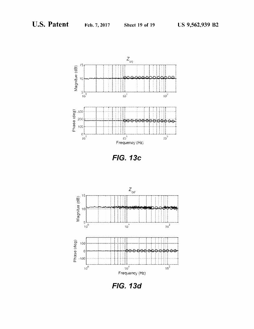
results, as shown in FIGS. 13a-13d.FIGS. 13a-13d illustrate example extracted impedances
of an input impedance of a dioderectifier, consistent with
certain disclosed embodiments. In FIGS. 13a-13d, a non-linear load is applied and a diode bridge is measured. The
obtained measurement results of FIGS. 13a-13d are com-pared with impedances extracted from a switching model
using a sinusoidal injection AC sweep algorithm.Theidentification and subsequent measurement of source
and load impedances are useful tools for assessing and
evaluating stability of electrical power systems. Stability canbe assessed by frequency domain analysis of the “minor
loop gain” transfer function, which is defined as the Z./Z,impedance ratio. In order to measure source and load
impedanceat an AC electrical system interface, a perturba-tion is injected in the direct and quadrature (dq) reference
frame. The voltage and current responseto the perturbation
are then measured. This measured data is post processed toobtain the spectra ofthe voltages and currents which are then
used to calculate Z,, and Z,;.When using only the shunt mode, at AC interfaces, the
source impedance is usually much smaller than the load
impedance because most of the injected current flows intothe low impedancesource side. The high impedance load
side is not disturbed enough resulting in a low Signal-to-Noise Ratio (SNR) which is not good for measurement
accuracy. An improvement in the load side SNR can berealized using a combination of shuntandseries injections.
That is, the disclosed embodiments include the additional
application of a series injection mode when measuring thehigh impedanceside (typically the load side in AC systems),
wherein instead of injecting perturbation current, a voltageperturbation is used. In this way, mostof the injected power
flows to the higher impedance Load side thereby raising theload side measurement SNR, which results in a more accu-
rate measurement.
While the foregoing written description of the inventionenables one of ordinary skill to make and use what is
considered presently to be the best mode thereof, those ofordinary skill will understand and appreciate the existence of
variations, combinations, and equivalents of particular dis-closed embodiments, systems, methods. The invention
should therefore not be limited by the described embodi-
ments, but by all embodiments and methods within the scopeand spirit of the invention.
Whatis claimed is:1. A method of impedance measurement in a three-phase
alternating current (AC) system, the method comprising:connecting a perturbation injector to the three-phase AC
system, the perturbation injector comprising a voltage
source inverter having a shunt injection circuit and aseries injection circuit that are operable without active
DC power addition;
10
15
20
25
30
35
40
45
50
55
60
65
16connecting by the perturbation injector the shunt injection
circuit to the three-phase AC system;
injecting by the shunt injection circuit a shunt perturba-
tion signal into the three-phase AC system;
collecting by a collection circuit of an impedance mea-
surement unit a response to the shunt perturbation
signal;
switching by the perturbation injector from the shunt
injection circuit to the series injection circuit;
injecting by the series injection circuit a series perturba-
tion signal into the three-phase AC system;
collecting by the collection circuit of the impedancemeasurement unit a response to the series perturbation
signal;
transferring by an instrumentation platform computer theresponse to the shunt perturbation signal and the
response to the series perturbation signal from three-phase (abc) coordinates to direct and quadrature (dq);
and
calculating by a control circuit at least one impedance ofthe three-phase AC system based onthe responseto the
shunt perturbation signal and the responseto the seriesperturbation signal.
2. The method of claim 1, wherein the shunt perturbationsignal is configured according to the following:
rae ol
Isq(S)| = Ziaq(8)(Zsdq(S) + Zrag(s))' | Ipo(s)
ne nol
Itq(s)| = Zsaq(s)(Zsdg(8) + Ztag(S)) | Ipals)
where Z,,,(8) is a source impedance matrix, Z;4,(S) is aload impedance matrix, I,{s) is a d-axis source current,
I,{s) 1s a q-axis source current, I,,{s) is a d-axisperturbation current, I,,,(s) is a q-axis perturbation
current, I,,(s) is a d-axis load current, and I,,(s) is aq-axis load current.
3. The method of claim 1, wherein the series perturbation
signal is configured according to the following:
Vsa(s)
Veg(s)
Vpa(s) |
Voq(s)
Vpals) |
Vpq(s)
| = Zsaq(s)(Zsdgl8) + Zidg(8))| |
Vials)
Vig(s)| = Ziaq(8)(Zsdq(S) + Zrag(s))' |
where Z,,,(8) is a source impedance matrix, Z;4,(S) is aload impedance matrix, V,(s) is a d-axis source volt-
age, V,,,(S) is a q-axis sourcevoltage, V,,(s) is a d-axisperturbation voltage, V,,,(s) 1s a q-axis perturbation
voltage, V;As) is a d-axis load voltage, and V,,(s) is a
q-axis load voltage.4. The method of claim 1, wherein the series perturbation
signal is of the form:
fi -fo nh)x(t) = sin(2n{fo + OF
where f, is a start frequency, f, is an end frequency, T isa duration ofat least one ofthe first perturbation signal
and the second perturbation signal; and t is a time.

US 9,562,939 B2
175. The method of claim 1, wherein the action of transfer-
ring the response to the shunt perturbation signal and theresponse to the series perturbation signal from abe coordi-nate to dq coordinates comprises:
transforming anAC voltage to direct current (DC) voltagecomponents; and
transforming an AC current to DC current components.6. The method of claim 1, wherein the action of calcu-
lating at least one impedanceofthe three-phase AC systemcomprises:
identifying frequency points of interest; andcalculating impedanceat each identified frequency point.7. A system for performing impedance measurementin a
three-phase alternating current (AC) system, comprising:a perturbation injector connectable to the three-phase AC
system, the perturbation injector comprising a voltagesource inverter having a shunt injection circuit config-ured to inject a shunt perturbation signal into thethree-phase AC system and aseries injection circuitconfigured to inject a series perturbation signal into thethree-phase AC system, the voltage source inverterbeing selectively switchable from the shunt injection
circuit to the series injection circuit, both of which areoperable without active DC power addition;
a collection circuit configured to collect a response to the
shunt perturbation signal and a response to the seriesperturbation signal; and
a control unit configured to transfer the response to theshunt perturbation signal and the responseto the series
perturbation signal from three-phase (abc) coordinatesto direct and quadrature (dq) and to calculate at least
one impedance ofthe three-phase AC system based on
the response to the first perturbation signal and theresponse to the second perturbation signal.
8. The system of claim 7, wherein the shunt injectioncircuit is configured to inject the shunt perturbation signal
according to the following:
Isa(s) Tyas) || = Zpaql8)(Zsdq(s) + Ziag(s)) | |Jags) Ing (8)
nals) | foals)Ig(s) | = Lsaq8)(Zsdq(S) + Zidqls)) Ing(S)
10
15
20
25
30
35
40
18where Zsaq(S) isa source impedance matrix, Zrag(S) 18 a
load impedance matrix, I,(s) is a d-axis source current,
I,(s) is a q-axis source current, Las) is a d-axis
perturbation current, I,,(s) is a q-axis perturbation
current, I,(s) is a d-axis load current, and I,,(s) is a
q-axis load current.
9. The system of claim 7, wherein the series injection
circuit is configured to inject the series perturbation signal
according to the following:
Vsa(s) Vpa(s) |
Veg(s) Vg (5)
Vpals) |
Vpq(s)
| = Zsaq(s)(Zsdgl8) + Zidg(8))| |
Vials)Vi9(5) | = Ziaq(8)(Zsdq(S) + Zrag(s))' |
where Z,,,(8) is a source impedance matrix, Z;4,(S) is a
load impedance matrix, V,(s) 1s a d-axis source volt-
age, V,,(s) is a q-axis source voltage, V,,,(s) 1s a d-axis
perturbation voltage, V,,, (s) is a q-axis perturbation
voltage, V;As) is a d-axis load voltage, and V,,(s) is a
q-axis load voltage.
10. The system ofclaim 7, wherein the series perturbation
signal is of the form:
fi-fo i}x(t) = sin(2af + oT
where f, is a start frequency, f, is an end frequency, T isa duration ofat least one ofthe first perturbation signal
and the second perturbation signal; and t is a time.
11. The system of claim 7, wherein the control unit is
configured to transform anAC voltageto direct current (DC)voltage components, and transform an AC current to DC
current components.
12. The system of claim 7, wherein the control unit isconfigured to calculate the impedances of the three-phase
AC system at each frequency point.
* * * * *