A WIRELESS ENTRYPHONE SYSTEM IMPLEMENTATION WITH MSP430 ... · PDF filea wireless entryphone...
100
A WIRELESS ENTRYPHONE SYSTEM IMPLEMENTATION WITH MSP430 AND CC1100 By Bilal HATİPOĞLU Engineering Project Report Yeditepe University Faculty of Engineering and Architecture Department of Computer Engineering 2008
Transcript of A WIRELESS ENTRYPHONE SYSTEM IMPLEMENTATION WITH MSP430 ... · PDF filea wireless entryphone...
A WIRELESS ENTRYPHONE SYSTEM
IMPLEMENTATION WITH MSP430 AND CC1100
By
Bilal HATİPOĞLU
Engineering Project Report
Yeditepe University
Faculty of Engineering and Architecture
Department of Computer Engineering
2008
ii
A WIRELESS ENTRYPHONE SYSTEM
IMPLEMENTATION WITH MSP430 AND CC1100
APPROVED BY:
Assoc. Prof. Dr. Mustafa TÜRKBOYLARI …………………………
(Supervisor)
Assoc. Prof. Dr. Esin ONBAŞIOĞLU …………………………
Assoc. Prof. Dr. Ali SEZGİN …………………………
DATE OF APPROVAL: 28.05.2008

iii
ACKNOWLEDGEMENTS
Many thanks to my supervisor, Mustafa Turkboylari, for spending his weeks to
design the hardware and spending his days (not hours) for debugging the hardest hardware
problems with me, for his excessive effort on completion of the project and also for his
financial support on the project.
iv
ABSTRACT
A WIRELESS ENTRYPHONE SYSTEM IMPLEMENTATION USING
MSP430 AND CC1100
In current days, wireless communication is widespread and it is started to be used in
everyday life, for example, next-generation smart home automation systems widely use
wireless communication. People want smart systems to make their life easy, and we want
to discard the cables that limit our mobility.
Although most of the time standards like Wifi or ZigBee are used, sometimes it is
necessary to design a custom protocol. Because, every single solution has its own
characteristic, and most of the time, a customized protocol is more efficient in
functionality, but less efficient in means of development time and money.
In this project, we implemented a wireless entryphone system that it pretty similar to
its cabled version that is widely used in our country. So, it will be pretty easy and cost
efficient to set up or remove such a system in a home or apartment. We used TI’s MSP430
Microcontroller and Chipcon’s CC1100 RF Transceiver, and we designed our own
protocol for wireless communication. We implemented ADPCM Encoding as voice codec.
We also implemented XXTEA Encryption to provide security. This system is an example
of two way, half-duplex, multi-to-single-point communication. This system is pretty cheap,
easy to set up, very low power and secure.
v
ÖZET
MSP430 VE CC1100 ILE KABLOSUZ DIAFON SISTEMI
UYGULAMASI
Günümüzde, kablosuz teknolojiler gittikçe daha fazla önem kazanarak kablolu
teknolojilerin yerini almaya başladı. Bunun temel sebebi, taşınabilirliği, uygulanması kolay
olması ve çok kullanışlı olması.
Hayatımızı her yönden kolaylaştıran bu sistemler için geliştirilen çeşitli protokoller
ve bu protokolleri kullanan çeşitli sistemler mevcuttur. Ancak çoğu zaman, ihtiyaca gore
kendi protokolünüzü yazmanız daha verimli olmaktadır. Bu proje çerçevesinde, kendi
protokolümüzü oluşturarak, apartmanlarımızda veya evlerimizde kullandığımız diafonların
kablosuz olarak birbirleriyle haberleşebileceği bir sistem geliştirdik. Bu sistem sayesinde,
uygulaması çok kolay bir şekilde yapılabilecek, daireler-evler arasında hiçbir kablo
döşeme vs. ihtiyacı olmayan bir ürün ortaya çıkardık. Bu ürünümüz, ses kodlaması için 32
kbit/s ADPCM formatını kullanmaktadır. Ayrıca, havadaki haberleşmenin güvenli
olabilmesi ve başka kişiler tarafından dinlenememesi için XXTEA şifreleme sistemini
kullandık.
Proje kapsamında, genel sistemin yanında, gömülü ortamda C kodu ile ADPCM ses
kodlaması algoritması ve XXTEA şifreleme algoritması kodlanmıştır. Aynı zamanda,
kullanılan mikroişlemcinin çeşitli modülleri için sürücüler kodlanmıştır. Bütün yazılım,
çok kolay geliştirilebilecek ve istenilen özellikler kolaylıkla seçilebilecek modüllere
ayrılmıştır.
Bu tez, geliştirdiğimiz protokolümüzün ve yazılım uygulamamızın özelliklerini ve
iyi bilinen ADPCM ses kodlama sistemi ile XXTEA şifreleme sisteminin uygulanması ile
ilgili ayrıntıları kapsamaktadır.
vi
TABLE OF CONTENTS
ACKNOWLEDGEMENTS ............................................................................................. III
ABSTRACT....................................................................................................................... IV
ÖZET ...................................................................................................................................V
LIST OF FIGURES.......................................................................................................... IX
LIST OF TABLES............................................................................................................ XI
LIST OF SYMBOLS / ABBREVIATIONS...................................................................XII
1. INTRODUCTION .........................................................................................................14
1.1. ORGANIZATION OF REPORT........................................................................................14
1.2. USED SOFTWARE & APPLICATIONS............................................................................14
2. BACKGROUND ............................................................................................................15
2.1. ENTRYPHONE SYSTEM DESCRIPTION .........................................................................15
2.1.1. Wired Intercoms ................................................................................................16
2.1.2. Wireless Intercoms ............................................................................................17
2.2. WIRELESS COMMUNICATION PRINCIPLES ..................................................................17
2.2.1. History ...............................................................................................................19
2.2.2. Electromagnetic Spectrum.................................................................................19
2.2.3. Digital Wireless Communication.......................................................................20
2.3. VOICE CODING...........................................................................................................22
2.3.1. Turning Speech into Electrical Pulses ...............................................................23
2.3.2. Converting electrical impulses to digital signals - Voice coding ......................24
2.4. AUDIO COMPRESSION – THEORY AND PRINCIPLES.....................................................25
2.4.1. Lossless Compression of Audio ........................................................................26
2.4.2. Lossy Compression of Audio ............................................................................27
2.5. CRYPTOGRAPHY.........................................................................................................28
2.5.1. Symmetric-Key Cryptography...........................................................................29
3. HARDWARE DESCRIPTION ....................................................................................32
3.1. DEVELOPMENT BOARDS ............................................................................................32
vii
3.2. PROCESSING UNIT – MSP430 MCU ..........................................................................34
3.2.1. Key Features ......................................................................................................35
3.2.2. History of MSP430 ............................................................................................36
3.2.3. Pros ....................................................................................................................37
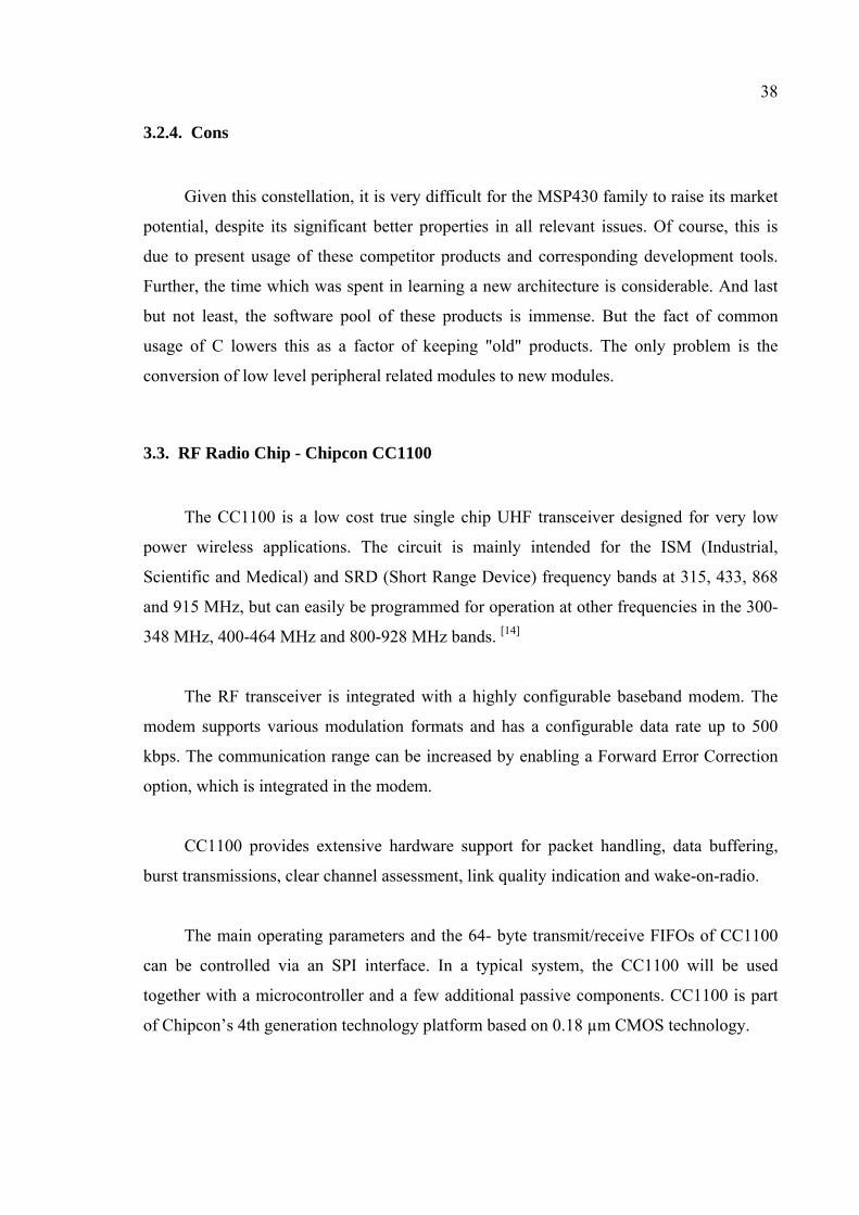
3.2.4. Cons ...................................................................................................................38
3.3. RF RADIO CHIP - CHIPCON CC1100 ..........................................................................38
3.3.1. Key Features / Benefits......................................................................................39
3.3.2. Used Features.....................................................................................................41
3.3.2.1. Radio State Machine...................................................................................41
3.3.2.2. Data FIFO ...................................................................................................42
3.3.2.3. Packet Format .............................................................................................42
3.3.2.4. Wake-on-Radio...........................................................................................45
3.3.2.5. Forward Error Correction ...........................................................................45
3.4. OTHER PERIPHERAL COMPONENTS ............................................................................46
3.4.1. LCD ...................................................................................................................46
3.4.2. Audio I/O Circuitry............................................................................................48
3.5. SUMMARY OF HARDWARE FEATURES ........................................................................48
4. SOFTWARE DESCRIPTION......................................................................................50
4.1. DESCRIPTION OF THE APPLICATION............................................................................50
4.2. SOFTWARE STATE MACHINE......................................................................................51
4.2.1. Entryphone Master Mode ..................................................................................52
4.2.2. Entryphone Slave Mode.....................................................................................55
4.2.3. Walkie-Talkie Mode ..........................................................................................56
4.3. TRANSMISSION PROTOCOL.........................................................................................56
4.3.1. Basic Transmission Scenario .............................................................................57
4.3.2. Packet Format ....................................................................................................60
4.3.3. Transmission / Data Rate Requirements............................................................61
4.4. DEVICE DRIVER IMPLEMENTATIONS ..........................................................................61
4.4.1. DMA Controller.................................................................................................62
4.4.2. Timer Module ....................................................................................................62
4.4.3. USART Peripheral Interface..............................................................................63
4.4.4. ADC Module......................................................................................................63
4.4.5. DAC Module......................................................................................................64

viii
4.5. BUFFERING MECHANISM............................................................................................64
4.6. AUDIO COMPRESSION AND VOICE ENCODING / DECODING........................................66
4.6.1. Sampling Theory and Implementation ..............................................................66
4.6.2. The ADPCM Codec...........................................................................................68
4.6.2.1. Implementation ...........................................................................................68
4.7. SECURITY IMPLEMENTATION AND ENCRYPTION ........................................................71
4.7.1. Attacks and Risks...............................................................................................71
4.7.2. Tiny Encryption Algorithm and Variants ..........................................................72
4.7.2.1. Implementation ...........................................................................................73
4.7.2.2. Key Features & Benefits.............................................................................74
5. ANALYSIS .....................................................................................................................75
5.1. MEMORY USAGE / REQUIREMENTS ............................................................................75
5.2. CPU USAGE ANALYSIS..............................................................................................76
5.3. CPU TIMING ..............................................................................................................77
5.4. POWER CONSUMPTION...............................................................................................80
5.4.1. CPU....................................................................................................................80
5.4.2. Radio Chip .........................................................................................................81
6. CONCLUSION ..............................................................................................................82
6.1. FURTHER DEVELOPMENT ...........................................................................................83
APPENDIX A: THE DPCM AND ADPCM CODECS..................................................84
APPENDIX B: XXTEA ENCRYPTION ALGORITHM ..............................................94
REFERENCES...................................................................................................................99
ix
LIST OF FIGURES
Figure 2.1: Electromagnetic Spectrum ................................................................................20
Figure 2.2: Quantization ......................................................................................................24
Figure 2.3: Digital Representation of Audio Signals...........................................................26
Figure 2.4: Basic principles of lossless audio compression.................................................27
Figure 3.1: First revision of development board..................................................................32
Figure 3.2: Second revision of the board. ............................................................................33
Figure 3.3: Chipcon CC1100 RF Module............................................................................34
Figure 3.4: Simplified block diagram of CC1100. ..............................................................39
Figure 3.5: Packet Format....................................................................................................44
Figure 3.6: Picture of the LCD display................................................................................47
Figure 3.7: Audio Circuitry .................................................................................................48
Figure 4.1: System block diagram. ......................................................................................50
Figure 4.2: Entryphone master mode state machine............................................................52
Figure 4.3: Entryphone slave mode state machine. .............................................................55
Figure 4.4: Walkie-Talkie mode state machine. ..................................................................56
Figure 4.5: Transmission flowchart. ....................................................................................59
Figure 4.6: Packet Format....................................................................................................60
Figure 4.7: Circular buffer structure. ...................................................................................65
Figure 4.8: The ADPCM stepsize adaptation. .....................................................................69
Figure 4.9: IMA ADPCM quantization . .............................................................................70
Figure 5.1: Transmit time chart. ..........................................................................................78
Figure 5.2: Receive time chart. ............................................................................................79
Figure A.1: Sampling and quantization of a sine wave for 4-bit PCM. ..............................84
Figure A.2: DPCM Encoder block diagram. .......................................................................86
Figure A.3: DPCM decoder block diagram. ........................................................................87
Figure A.4: Comparison of 8-bit audio data and difference of successive samples. ...........88
Figure A.5: ADPCM encoder and decoder block diagram..................................................90
Figure A.6: IMA ADPCM stepsize adaptation....................................................................92
Figure A.7: IMA ADPCM quantization. .............................................................................93
Figure B.1: Two rounds of the Tiny Encryption Algorithm................................................94
x
Figure B.2: Two rounds of the XTEA block cipher. ...........................................................96
Figure B.3: XXTEA cipher..................................................................................................97
xi
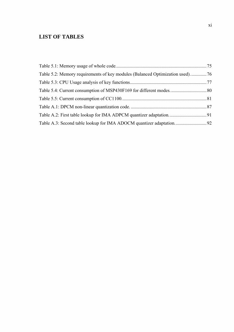
LIST OF TABLES
Table 5.1: Memory usage of whole code.............................................................................75
Table 5.2: Memory requirements of key modules (Balanced Optimization used). .............76
Table 5.3: CPU Usage analysis of key functions.................................................................77
Table 5.4: Current consumption of MSP430F169 for different modes. ..............................80
Table 5.5: Current consumption of CC1100........................................................................81
Table A.1: DPCM non-linear quantization code. ................................................................87
Table A.2: First table lookup for IMA ADPCM quantizer adaptation. ...............................91
Table A.3: Second table lookup for IMA ADOCM quantizer adaptation...........................92

xii
LIST OF SYMBOLS / ABBREVIATIONS
ADC Analog-to-digital Converter
ADPCM Adaptive Differential Pulse Code Modulation
AES Advanced Enrcyption Standard
AM Amplitude Modulation
ASIC Application Specific Integrated Circuits
BSL Bootstrap Loader
CCA Clear Channel Assessment
CPU Central Processing Unit
CRC Cyclic Redundancy Check
CTS Clear to Send
DAC Digital-to-analog Converter
DES Data Encryption Standard
DMA Direct Memory Access
DPCM Differential Pulse Code Modulation
DSP Digital Signal Processor
EPROM Erasable Programmable Read-Only Memory
FIFO First-in-first-out
FM Frequency Modulation
FPGA Field-Programmable Gate Array
HAL Hardware Abstraction Library
I2C Inter-Integrated Circuit
IMA Integrated Media Association
IRDA Infrared Data Association
LCD Liquid Crystal Display
LED Light Emitting Diode
LPCM Linear Pulse Code Modulation
MCU Microcontroller Unit
MIPS Million Instructions per Second,
MSK Minimum Shift Keying
PAM Pulse-Amplitude Modulation
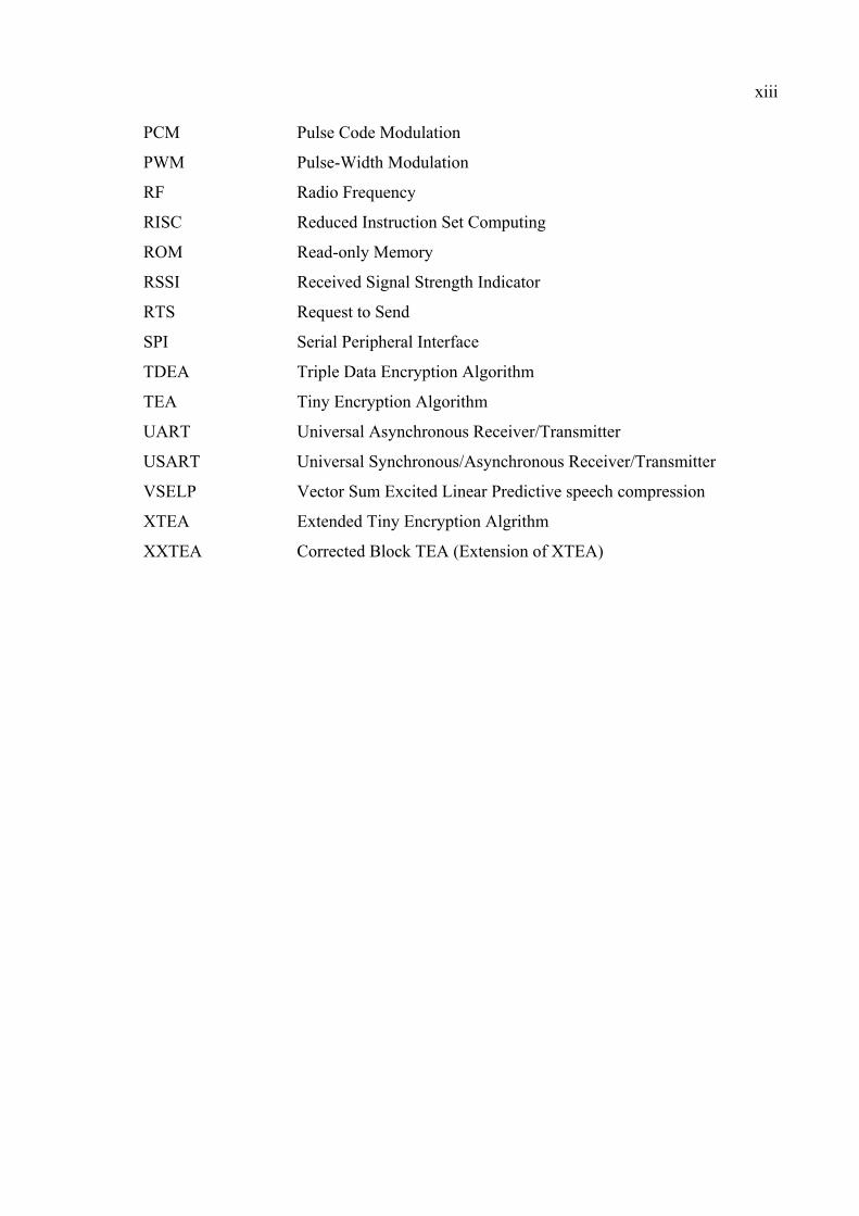
xiii
PCM Pulse Code Modulation
PWM Pulse-Width Modulation
RF Radio Frequency
RISC Reduced Instruction Set Computing
ROM Read-only Memory
RSSI Received Signal Strength Indicator
RTS Request to Send
SPI Serial Peripheral Interface
TDEA Triple Data Encryption Algorithm
TEA Tiny Encryption Algorithm
UART Universal Asynchronous Receiver/Transmitter
USART Universal Synchronous/Asynchronous Receiver/Transmitter
VSELP Vector Sum Excited Linear Predictive speech compression
XTEA Extended Tiny Encryption Algrithm
XXTEA Corrected Block TEA (Extension of XTEA)
14
1. INTRODUCTION
1.1. Organization of Report
The organization of this thesis is as follows: Chapter 2 contains the purpose and
scope of the project with background information about Entryphone System, Wireless
Communication, Audio Compression and Encryption. Chapter 3 is the Hardware
Description part that contains the description of the used hardware components and board.
Chapter 4 contains the Software Description, including the architecture of designed
software, state machine of application, definition of used protocols, voice coding and
encryption, and device driver implementations. Chapter 5 contains detailed analysis of
Memory and CPU usage of the software and Power consumption of the hardware. Chapter
6 is the conclusion part, containing the summary of results, possible problems with or
without implementation of solutions and further improvement suggestions. After the report
body, there are Appendices sections. Appendix A contains the details of ADPCM voice
codec and IMA ADPCM implementation that is used in the project, and finally Appendix
B covers the details of used encryption algorithm, that is called Extended Block TEA
(XXTEA) algorithm and its background.
1.2. Used Software & Applications
For the implementation phase of the project, I have used IAR Embedded Workbench
for code development, simulation and analysis. The code is compiler dependent, and only
implemented for IAR Compiler. But the code can be easily ported to another desired
compiler with minor modifications. I also used Texas Instruments’ SmartRF Studio
application to generate the settings and parameters for wireless transmission.
15
2. BACKGROUND
2.1. Entryphone System Description
An intercom (intercommunication device) is an electronic communications system
intended for limited or private dialogue, direction, collaboration or announcements.
Intercoms can be portable or mounted permanently in buildings and vehicles. Intercoms
can incorporate connections to walkie talkies, telephones, cell phones and to other
intercom systems over phone or data lines and to electronic or electro-mechanical devices
such as signal lights and door latches.
Home intercom and security systems for buildings are used for communication
between households and visitors or guards; they offer talk-back, entrance guard and
security management. In Europe, as houses are mostly of the villa type, the home intercom
emphasizes high stability. In Asian cities many people are living in big apartment blocks
with a hundred or more families, and the home intercom emphasizes multi-functionality
for many users. [1]
Entryphone is an intercom device that is used in the apartments or buildings, to
communicate with the person who is at outside the door. Entryphone systems are usually
interfacing with the building's access control system or doorbell. It is a simple intercom
device, since a small home intercom might connect a few rooms in a house. Larger systems
might connect all of the rooms in a school or hospital to a central office. Intercoms in
larger buildings often function as public address systems, capable of broadcasting
announcements. Intercom systems can be found on many types of vehicles including trains,
watercraft, aircraft and armoured fighting vehicles.
Permanent intercoms installed in buildings are generally composed of fixed
microphone/speaker units which connect to a central control panel by wires.
16
Traditional intercom systems are composed entirely of analogue electronics
components but many new features and interfacing options can be accomplished with new
intercom systems based on digital connections. Video signals can be interlaced with the
more familiar audio signals. Digital intercom stations can be connected using Cat 5 cable,
IP subsystem or can even use existing computer networks as a means of interfacing distant
parties.
2.1.1. Wired Intercoms
While every intercom product line is different, most analogue intercom systems have
much in common. Voice signals of about a volt or two are carried atop a direct current
power rail of 12, 30 or 48 volts which uses a pair of conductors. Signal light indications
between stations can be accomplished through the use of additional conductors or can be
carried on the main voice pair via tone frequencies sent above or below the speech
frequency range. Multiple channels of simultaneous conversations can be carried over
additional conductors within a cable or by frequency- or time-division multiplexing in the
analogue domain. Multiple channels can easily be carried by packet-switched digital
intercom signals.
Portable intercoms are connected primarily using common shielded, twisted pair
microphone cabling. Building and vehicle intercoms are connected in a similar manner
with shielded cabling often containing more than one twisted pair.
Some digital intercoms use Category 5 cable and relay information back and forth in
data packets using the Internet protocol architecture.
Most of the time, it is hard to install an intercom system through a building or
apartment, because of the cabling effort.
17
2.1.2. Wireless Intercoms
For installations where it is not desirable or possible to run wires to support an
intercom system, wireless intercom systems are available. There are two major benefits of
a wireless intercom system over the traditional wired intercom. The first is that installation
is much easier since no wires have to be run between intercom units. The second is that
you can easily move the units at any time. With that convenience and ease of installation
comes a risk of interference from other wireless and electrical devices. Nearby wireless
devices such as cordless telephones, wireless data networks, and remote audio speakers can
interfere. Electrical devices such as motors, lighting fixtures and transformers can cause
noise. There may be concerns about privacy since conversations may be picked up on a
scanner, baby monitor, cordless phone, or a similar device on the same frequency.
Encrypted wireless intercoms can reduce or eliminate privacy risks, while placement,
installation, construction, grounding and shielding methods can reduce or eliminate the
detrimental effects of external interference. [2]
Our implementation is a Digital Wireless Intercom system, that uses a hardware
configurable frequency channel (in this project we used 433 MHz ISM band). We provide
digital voice coding with Adaptive Differential Pulse Code Modulation (ADPCM)
algorithm, and we provide security with Extended Block Tiny Encryption Algorithm
(XXTEA).
2.2. Wireless Communication Principles
The term “wireless” is normally used to refer to any type of electrical or electronic
operation which is accomplished without the use of a "hard wired" connection. Wireless
communication is the transfer of information over a distance without the use of electrical
conductors or "wires". The distances involved may be short (a few meters as in television
remote control) or very long (thousands or even millions of kilometers for radio
communications). When the context is clear the term is often simply shortened to
"wireless". Wireless communications is generally considered to be a branch of
telecommunications. [3]

18
It encompasses various types of fixed, mobile, and portable two way radios, cellular
telephones, personal digital assistants (PDAs), and wireless networking. Other examples of
wireless technology include GPS units, garage door openers and or garage doors, wireless
computer mice and keyboards, satellite television and cordless telephones.
The term "wireless" has become a generic and all-encompassing word used to
describe communications in which electromagnetic waves or RF (rather than some form of
wire) carry a signal over part or the entire communication path.
Wireless communication may be implemented via:
1- Radio frequency (RF) communication,
2- Microwave communication, for example long-range line-of-sight via highly
directional antennas, or short-range communication, or
3- Infrared (IR) short-range communication, for example from remote controls or via
IRDA.
A wireless communication system deals with two directions, a transmitting direction
and a receiving direction. Normally, the size of the antenna must be as large as one fourth
of the wavelength of the signal to be transmitted or received to get enough efficiency. For
this reason, the original signal (normally the voice) with a large wavelength must be
transferred to a higher frequency (smaller wavelength) to downsize the antenna. At the
transmitting end, the original signal is imposed on a locally generated radio frequency (RF)
signal called a carrier. This process is called modulation.
This carrier signal, along with the information signal imposed on it, is then radiated
by the antenna. At the receiving end, the signal is picked up by another antenna and fed
into a receiver where the desired carrier with the imposed information signal is selected
from among all of the other signals impinging on the antenna. The information signal (e.g.,
voice) is then extracted from the carrier in a process referred to as demodulation.
The propagation of the signal in free space is not fluent. There may be some negative
influence to the received signal. First, the signal becomes weaker and weaker during the
propagation. Second, interference from some noise will distort the information signal; An
19
then, some propagation mechanisms such as reflection, diffraction and scattering, will
distort the information signal too. It is even worse in mobile systems -- where one or both
of the terminals (transmitters and receivers) can move about -- due to an environment that
changes dynamically from moment to moment. To get rid of these problems, we need more
precise models to describe the propagation, and more modulation technology to avoid
distortion.
2.2.1. History
The term "Wireless" came into public use to refer to a radio receiver or transceiver (a
dual purpose receiver and transmitter device), establishing its usage in the field of wireless
telegraphy early on; now the term is used to describe modern wireless connections such as
in cellular networks and wireless broadband Internet. It is also used in a general sense to
refer to any type of operation that is implemented without the use of wires, such as
"wireless remote control", "wireless energy transfer", etc. regardless of the specific
technology (e.g., radio, infrared, ultrasonic, etc.) that is used to accomplish the operation.
2.2.2. Electromagnetic Spectrum
Light, colors, AM and FM radio and electronic devices make use of the
electromagnetic spectrum. In the US the frequencies that are available for use for
communication are treated as a public resource and are regulated by the Federal
Communications Commission. This determines which frequency ranges can be used for
what purpose and by whom. In the absence of such control or alternative arrangements
such as a privatized electromagnetic spectrum, chaos might result if, for example, airlines
didn't have specific frequencies to work under and an amateur radio operator was
interfering with the pilot's ability to land an airplane. Wireless communication spans the
spectrum from 9 kHz to 300 GHz. The International Telecommunications Union (ITU) is
the part of the United Nations (UN) that manages the use of both the RF Spectrum and
space satellites among nation states. [4]
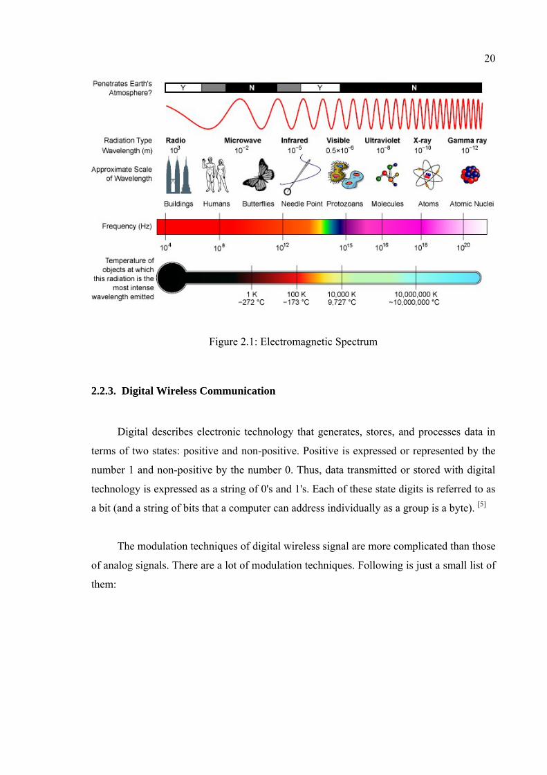
20
Figure 2.1: Electromagnetic Spectrum
2.2.3. Digital Wireless Communication
Digital describes electronic technology that generates, stores, and processes data in
terms of two states: positive and non-positive. Positive is expressed or represented by the
number 1 and non-positive by the number 0. Thus, data transmitted or stored with digital
technology is expressed as a string of 0's and 1's. Each of these state digits is referred to as
a bit (and a string of bits that a computer can address individually as a group is a byte). [5]
The modulation techniques of digital wireless signal are more complicated than those
of analog signals. There are a lot of modulation techniques. Following is just a small list of
them:
21
Linear Modulation Techniques:
BPSK : Binary Phase Shift Keying
DPSK : Differential Phase Shift Keying
QPSK : Quadrature Phase Shift Keying
Constant Envelope Modulation Techniques:
BFSK : Binary Frequency Shift Keying
MSK : Minimum Shift Keying
GMSK : Gaussian Minimum Shift Keying
Combined Linear and Constant Envelope Modulation Techniques:
MPSK : M-ary Phase Shift Keying
QAM : M-ary Quadrature Amplitude Modulation
MFSK : M-ary Frequency Shift Keying
Spread Spectrum Modulation Techniques:
DS-SS : Direct Sequence Spread Spectrum
FH-SS : Frequency Hopped Spread Spectrum
When wireless applications, such as mobile phones, were initially introduced into
society, they were based on analog technology, as the prime service was voice. Analog was
a suitable means, capable of delivering the service. However, the requirements &
expectations of the current consumer often exceed this service to include data as well. Thus
the market is being driven to satisfy the requirements of data & voice, which can be more
adequately delivered by digital technologies. Most consumers prefer digital to analog
because of its superior performance & service providers are embracing digital technologies
as well. By examination of the various advertising media nowadays, one can see that they
are attempting to convince their clients using analog to convert to digital. In a way, analog
can be looked on as a predecessor to digital in the field of wireless technologies.
22
Some advantages of digital wireless communication over analog:
• It economizes on bandwidth.
• It allows easy integration with personal communication systems (PCS)
devices.
• It maintains superior quality of voice transmission over long distances.
• It is difficult to decode.
• It can use lower average transmitter power.
• It enables smaller and less expensive individual receivers and transmitters.
• It offers voice privacy.
2.3. Voice Coding
Digital audio uses digital signals for sound reproduction. This includes analog-to-
digital conversion, digital-to-analog conversion, storage, and transmission.
Digital audio has emerged because of its usefulness in the recording, manipulation,
mass-production, and distribution of sound. Modern distribution of music across the
internet through on-line stores depends on digital recording and digital compression
algorithms. Distribution of audio as data files rather than as physical objects has
significantly reduced costs of distribution.
The objective of speech is communication whether face-to-face or cell phone to cell
phone. To fit a transmission channel or storage space, speech signals are converted to
formats using various techniques. This is called speech coding or compression. To improve
the efficiency of transmission and storage, reduce cost, increase security and robustness in
transmission, speech coding attempts to achieve toll quality performance at a minimum bit
rate. [6]
23
2.3.1. Turning Speech into Electrical Pulses
Speech is sound in motion. Talking produces acoustic pressure. Speaking into the
can of a string telephone, for example, makes the line vibrate, causing sound waves to
travel from one end of the stretched line to the other. A telephone by comparison,
reproduces sound by electrical means. What the Victorians called "talking by lightning." A
standard dictionary defines the telephone as "an apparatus for reproducing sound,
especially that of the voice, at a great distance, by means of electricity; consisting of
transmitting and receiving instruments connected by a line or wire which conveys the
electric current."
Electricity works the phone itself: operates the keypad, makes it ring. Electricity
provides a path, too, for voice and data to travel over wires. Electric current doesn't really
convey voice; sound merely varies the current. It's these electrical variations, analogs of
the acoustic pressure originally spoken into the telephone transmitter or microphone, which
represent voice.
In wireless technology, a coder inside the mobile telephone converts sound to digital
impulses on the transmitting side. On the receiving side it converts these impulses back to
analog sounds. A coder or vocoder is a speech analyzer and synthesizer in one. Vocoders
are in every digital wireless telephone, part of a larger chip set called a digital signal
processor. Sound gets modeled and transmitted on one end by the analyzer part of the
vocoder. On the receiving end the speech synthesizer part interprets the signal and
produces a close match of the original. Keep following along.
Digital signals are a mathematical or numerical representation of sound, with each
sonic nuance captured as a binary number. Reproducing sound is as easy as reproducing
the numbers. Extensive error checking schemes ensure that a wireless digital link stays
intact, even when transmitted through the air.
24
2.3.2. Converting electrical impulses to digital signals - Voice coding
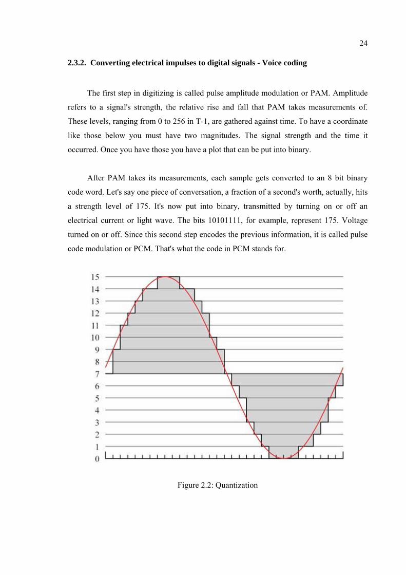
The first step in digitizing is called pulse amplitude modulation or PAM. Amplitude
refers to a signal's strength, the relative rise and fall that PAM takes measurements of.
These levels, ranging from 0 to 256 in T-1, are gathered against time. To have a coordinate
like those below you must have two magnitudes. The signal strength and the time it
occurred. Once you have those you have a plot that can be put into binary.
After PAM takes its measurements, each sample gets converted to an 8 bit binary
code word. Let's say one piece of conversation, a fraction of a second's worth, actually, hits
a strength level of 175. It's now put into binary, transmitted by turning on or off an
electrical current or light wave. The bits 10101111, for example, represent 175. Voltage
turned on or off. Since this second step encodes the previous information, it is called pulse
code modulation or PCM. That's what the code in PCM stands for.
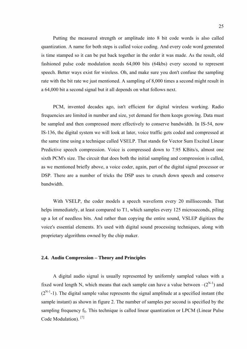
Figure 2.2: Quantization
25
Putting the measured strength or amplitude into 8 bit code words is also called
quantization. A name for both steps is called voice coding. And every code word generated
is time stamped so it can be put back together in the order it was made. As the result, old
fashioned pulse code modulation needs 64,000 bits (64kbs) every second to represent
speech. Better ways exist for wireless. Oh, and make sure you don't confuse the sampling
rate with the bit rate we just mentioned. A sampling of 8,000 times a second might result in
a 64,000 bit a second signal but it all depends on what follows next.
PCM, invented decades ago, isn't efficient for digital wireless working. Radio
frequencies are limited in number and size, yet demand for them keeps growing. Data must
be sampled and then compressed more effectively to conserve bandwidth. In IS-54, now
IS-136, the digital system we will look at later, voice traffic gets coded and compressed at
the same time using a technique called VSELP. That stands for Vector Sum Excited Linear
Predictive speech compression. Voice is compressed down to 7.95 KBits/s, almost one
sixth PCM's size. The circuit that does both the initial sampling and compression is called,
as we mentioned briefly above, a voice coder, again, part of the digital signal processor or
DSP. There are a number of tricks the DSP uses to crunch down speech and conserve
bandwidth.
With VSELP, the coder models a speech waveform every 20 milliseconds. That
helps immediately, at least compared to T1, which samples every 125 microseconds, piling
up a lot of needless bits. And rather than copying the entire sound, VSLEP digitizes the
voice's essential elements. It's used with digital sound processing techniques, along with
proprietary algorithms owned by the chip maker.
2.4. Audio Compression – Theory and Principles
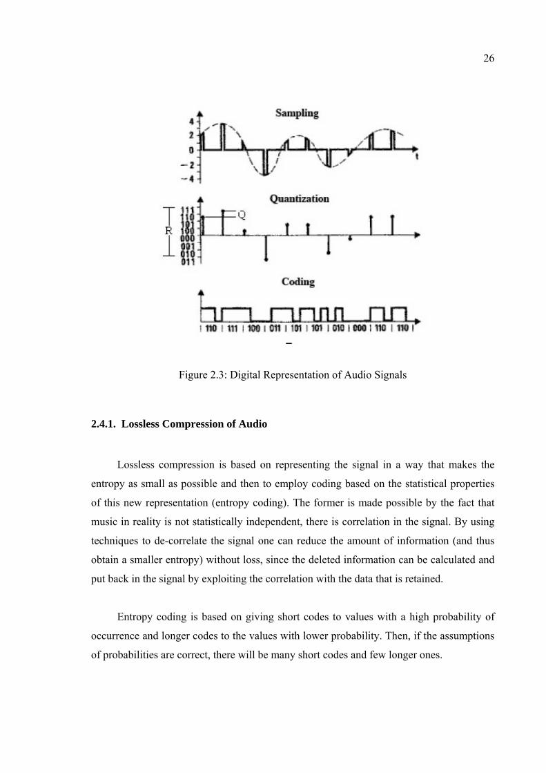
A digital audio signal is usually represented by uniformly sampled values with a
fixed word length N, which means that each sample can have a value between –(2N-1) and
(2N-1-1). The digital sample value represents the signal amplitude at a specified instant (the
sample instant) as shown in figure 2. The number of samples per second is specified by the
sampling frequency fS. This technique is called linear quantization or LPCM (Linear Pulse
Code Modulation). [7]
26
Figure 2.3: Digital Representation of Audio Signals
2.4.1. Lossless Compression of Audio
Lossless compression is based on representing the signal in a way that makes the
entropy as small as possible and then to employ coding based on the statistical properties
of this new representation (entropy coding). The former is made possible by the fact that
music in reality is not statistically independent, there is correlation in the signal. By using
techniques to de-correlate the signal one can reduce the amount of information (and thus
obtain a smaller entropy) without loss, since the deleted information can be calculated and
put back in the signal by exploiting the correlation with the data that is retained.
Entropy coding is based on giving short codes to values with a high probability of
occurrence and longer codes to the values with lower probability. Then, if the assumptions
of probabilities are correct, there will be many short codes and few longer ones.
27
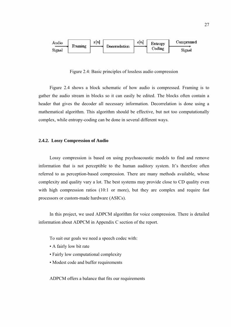
Figure 2.4: Basic principles of lossless audio compression
Figure 2.4 shows a block schematic of how audio is compressed. Framing is to
gather the audio stream in blocks so it can easily be edited. The blocks often contain a
header that gives the decoder all necessary information. Decorrelation is done using a
mathematical algorithm. This algorithm should be effective, but not too computationally
complex, while entropy-coding can be done in several different ways.
2.4.2. Lossy Compression of Audio
Lossy compression is based on using psychoacoustic models to find and remove
information that is not perceptible to the human auditory system. It’s therefore often
referred to as perception-based compression. There are many methods available, whose
complexity and quality vary a lot. The best systems may provide close to CD quality even
with high compression ratios (10:1 or more), but they are complex and require fast
processors or custom-made hardware (ASICs).
In this project, we used ADPCM algorithm for voice compression. There is detailed
information about ADPCM in Appendix C section of the report.
To suit our goals we need a speech codec with:
• A fairly low bit rate
• Fairly low computational complexity
• Modest code and buffer requirements
ADPCM offers a balance that fits our requirements
28
2.5. Cryptography
Cryptography, in Greek, literally means hidden writing, or the art of changing plain
textmessage. Cryptography is used increasingly by businesses, individuals and the
govemment for ensuring the security and privacy of information and communications.
Cryptography's use by criminals is becoming widespread as well. The same aspects of
cryptography that make it useful for security and privacy make it particutarly troublesome
for law enforcement. [8]
Cryptography is the practice and study of hiding information. In modern times,
cryptography is considered to be a branch of both mathematics and computer science, and
is affiliated closely with information theory, computer security, and engineering.
The need for cryptography is, today, arguably self-evident. However, the exact style
of cryptography is something varied; one can find examples of cryptographic algorithm
users who fall into the camps of desiring high speed without regard to power consumption,
those who desire ultra-low power consumption without the need for super high throughput,
and those who want it all.
Serious cryptanalysts such as government bodies and researchers typically end up
being limited by their available capital rather than the available power in the system (if you
can afford a massively parallel FPGA code breaker, you can probably afford the electricity
to power it). For such individuals, we offer a comparison of the raw speed of various
cryptosystems without regard to their power requirements.
Ultra-low power consumption is needed in devices that typically have little or no
battery power and/or recharging ability. Examples include ‘single use’ military sensors
that are interrogated via RF, ‘smart cards’ that are powered by a (very) low power incident
electromagnetic field, and ultra-miniature electronic devices such as pager watches, etc.
We will briefly review low-power design techniques and examine various low power
implementations in details.
Many everyday devices such as PDAs, laptop computers, and cell phones would
prefer to have their cake (high encryption speeds) and eat it too (as opposed to eating their
29
batteries). Although these devices have ‘reasonable’ energy stores (typically >=1000J), the
use cryptographic protocols can significantly influence the overall energy usage of the
device. One of the significant considerations in the case of these devices is whether a
hardware, software, or programmable logic solution is best at providing the necessary
cryptographic performance. We don’t consider the price of adding hardware (an ASIC or
FPGA), but we will show the performance they can add to the system.
2.5.1. Symmetric-Key Cryptography
Symmetric-key cryptography refers to encryption methods in which both the sender
and receiver share the same key (or, less commonly, in which their keys are different, but
related in an easily computable way). This was the only kind of encryption publicly known
until June 1976.
The modern study of symmetric-key ciphers relates mainly to the study of block
ciphers and stream ciphers and to their applications. A block cipher is, in a sense, a modern
embodiment of Alberti's polyalphabetic cipher: block ciphers take as input a block of
plaintext and a key, and output a block of ciphertext of the same size. Since messages are
almost always longer than a single block, some method of knitting together successive
blocks is required. Several have been developed, some with better security in one aspect or
another than others. They are the mode of operations and must be carefully considered
when using a block cipher in a cryptosystem.
The most commonly used conventional encryption algorithms are block ciphers. A
block cipher processes the plaintext input in fixed-size blocks and produces a block of
ciphertext of equal size for each plaintext block. The two most important conventional
algorithms, both of which are block ciphers, are the Data Encryption Standard (DES), and
Triple Data Encryption Algorithm (TDEA). [9]
The Data Encryption Standard (DES) and the Advanced Encryption Standard (AES)
are block cipher designs which have been designated cryptography standards by the US
government (though DES's designation was finally withdrawn after the AES was adopted).
Despite its deprecation as an official standard, DES (especially its still-approved and much
30
more secure triple-DES variant) remains quite popular; it is used across a wide range of
applications, from ATM encryption to e-mail privacy and secure remote access. Many
other block ciphers have been designed and released, with considerable variation in
quality. Many have been thoroughly broken.
Stream ciphers, in contrast to the 'block' type, create an arbitrarily long stream of key
material, which is combined with the plaintext bit-by-bit or character-by-character,
somewhat like the one-time pad. In a stream cipher, the output stream is created based on
an internal state which changes as the cipher operates. That state's change is controlled by
the key, and, in some stream ciphers, by the plaintext stream as well. RC4 is an example of
a well-known stream cipher.
In this project, we used Extended Block Tiny Encryption Algorithm (XXTEA). The
algorithm is explained on Appendix D in details. Tiny Encryption Algorithm (TEA) is a
block cipher notable for its simplicity of description and implementation (typically a few
lines of code). Executing encryption software on a microcontroller is a fine balance
between security level, size, and cycles. In general, the more secure an algorithm, the more
cycles that are required. The TEA was chosen because it offers the best security-to-cycles
ratio. As written, it does 32 iterations, with any single bit change in the input data being
fully propagated in 4 iterations. The security is similar to DES, but it is done with one-third
the cycles of DES. This is accomplished by using less-complicated equations but executing
more iterations.
Like TEA, XTEA is a 64-bit block Feistel network with a 128-bit key and a
suggested 64 rounds. Several differences from TEA are apparent, including a somewhat
more complex key-schedule and a rearrangement of the shifts, XORs, and additions. [10]
Presented along with XTEA was a variable-width block cipher termed Block TEA,
which uses the XTEA round function but applies it cyclically across an entire message for
several iterations. Because it operates on the entire message, Block TEA has the property
that it does not need a mode of operation. An attack on the full Block TEA was described
in (Saarinen, 1998), which also details a weakness in Block TEA's successor, XXTEA. [11]

31
Corrected Block TEA (often referred to as XXTEA) is a block cipher designed to
correct weaknesses in the original Block TEA (Tiny Encryption Algorithm). If the block
size is equal to the entire message, XXTEA has the property that it does not need a mode
of operation: the cipher can be directly applied to encrypt the entire message. XXTEA is
likely to be more efficient than XTEA for longer messages.
32
3. HARDWARE DESCRIPTION
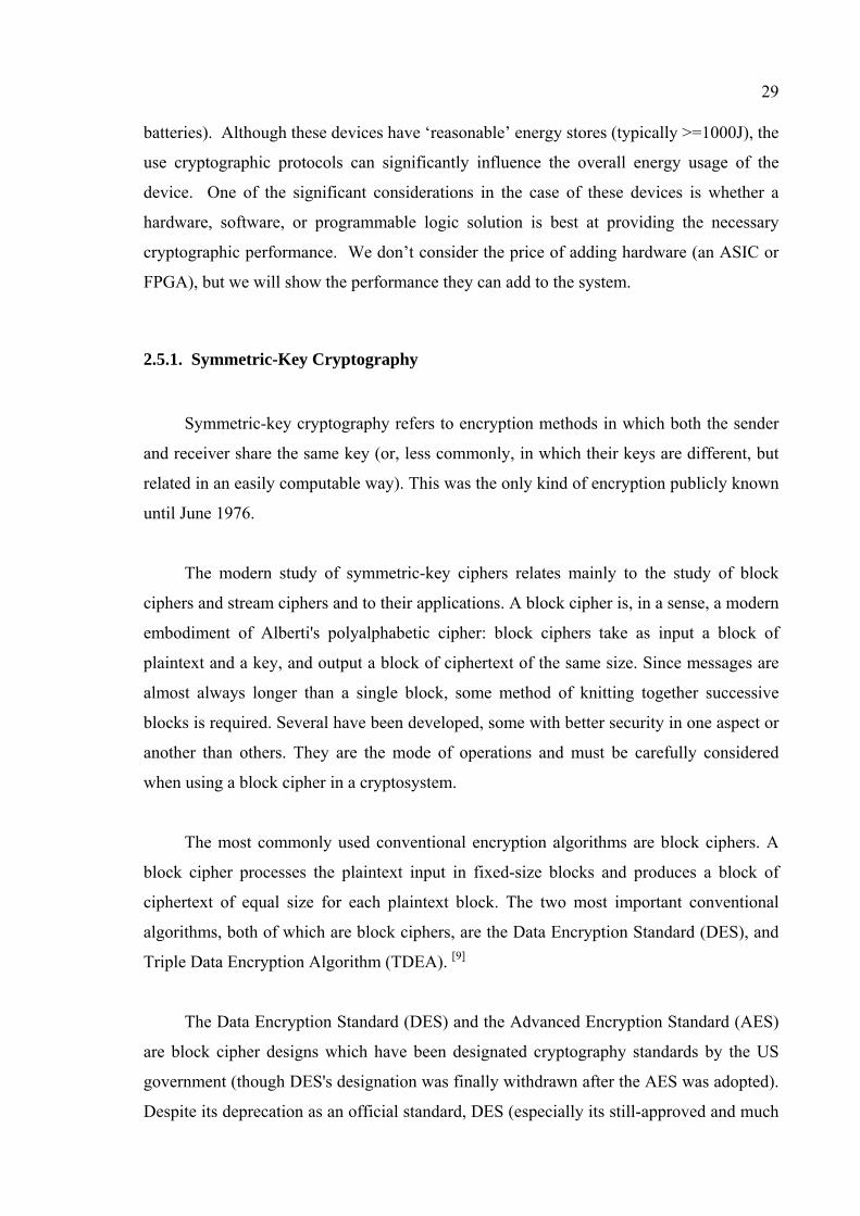
3.1. Development Boards
We have used two types of development board. First, we have the first revision that
has no audio I/O. We developed the network protocol on it. The second revision has audio
I/O and final development is done on that. Both boards are designed by my supervisor,
Mustafa Turkboylari.
Figure 3.1: First revision of development board.
Both boards has wireless module slot. Wireless chip is on removable modules (i.e.
daughter board). This daughter board is easily removable. Both revisions of boards have
LCD slot and UART connectivity on them. Also, both has configurable buttons.
33
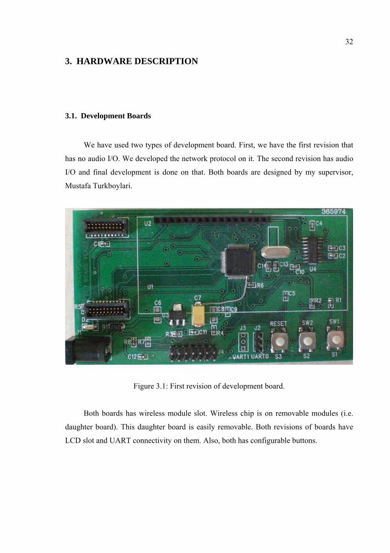
Figure 3.2: Second revision of the board.
Second revision of development board has both audio input and output jack and on-
board microphone and speaker. It also has two extra switches of 8 pins, and two LEDs.
The board has a connector for Chipcon’s RF modules and another connector for
Hitachi compatible LCD.
34
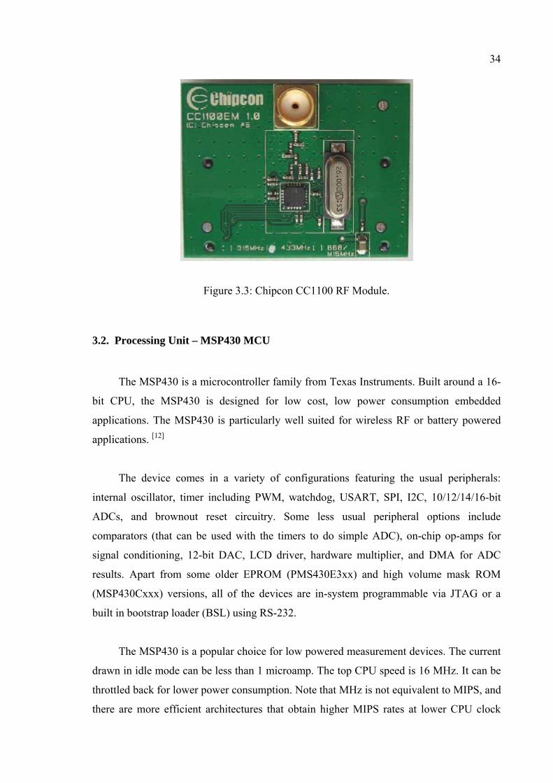
Figure 3.3: Chipcon CC1100 RF Module.
3.2. Processing Unit – MSP430 MCU
The MSP430 is a microcontroller family from Texas Instruments. Built around a 16-
bit CPU, the MSP430 is designed for low cost, low power consumption embedded
applications. The MSP430 is particularly well suited for wireless RF or battery powered
applications. [12]
The device comes in a variety of configurations featuring the usual peripherals:
internal oscillator, timer including PWM, watchdog, USART, SPI, I2C, 10/12/14/16-bit
ADCs, and brownout reset circuitry. Some less usual peripheral options include
comparators (that can be used with the timers to do simple ADC), on-chip op-amps for
signal conditioning, 12-bit DAC, LCD driver, hardware multiplier, and DMA for ADC
results. Apart from some older EPROM (PMS430E3xx) and high volume mask ROM
(MSP430Cxxx) versions, all of the devices are in-system programmable via JTAG or a
built in bootstrap loader (BSL) using RS-232.
The MSP430 is a popular choice for low powered measurement devices. The current
drawn in idle mode can be less than 1 microamp. The top CPU speed is 16 MHz. It can be
throttled back for lower power consumption. Note that MHz is not equivalent to MIPS, and
there are more efficient architectures that obtain higher MIPS rates at lower CPU clock
35
frequencies, which can result in lower dynamic power consumption for an equivalent
amount of processing. [13]
There are, however, limitations that prevent it from being used in more complex
embedded systems. The MSP430 does not have an external memory bus, so is limited to
on-chip memory (up to 120 KB Flash and 10 KB RAM) which might be too small for
applications that require large buffers or data tables.
The MSP430 CPU uses Von-Neumann architecture, with a single address space for
instructions and data. Memory is byte-addressed, and pairs of bytes are combined little-
endian to make 16-bit words.
The processor contains 16 16-bit registers. R0 is the program counter, R1 is the stack
pointer, R2 is the status register, and R3 is a special register called the constant generator,
providing access to 6 commonly used constant values without requiring an additional
operand. R4 through R15 are available for general use.
The instruction set is very simple; there are 27 instructions in three families. Most
instructions are available in 8-bit (byte) and 16-bit (word) versions, depending on the value
of a B/W bit - the bit is set to 1 for 8-bit and 0 for 16-bit. Byte operations to memory affect
only the addressed byte, while byte operations to registers clear the most significant byte.
3.2.1. Key Features
Key features of the MSP430x1xx family include:
• Ultralow-power architecture extends battery life
o 0.1-µA RAM retention
o 0.8-µA real-time clock mode
o 250-µA / MIPS active
36
• High-performance analog ideal for precision measurement
o 12-bit or 10-bit ADC — 200 ksps, temperature sensor, VRef
o 12-bit dual-DAC
o Comparator-gated timers for measuring resistive elements
o Supply voltage supervisor
• 16-bit RISC CPU enables new applications at a fraction of the code size.
o Large register file eliminates working file bottleneck
o Compact core design reduces power consumption and cost
o Optimized for modern high-level programming
o Only 27 core instructions and seven addressing modes
o Extensive vectored-interrupt capability
• In-system programmable Flash permits flexible code changes, field upgrades
and data logging
Details and specification of MSP430 is not included in this report. You can find very
detailed description and specifications of MSP430F169 in MSP430x1xx Family User
Guide and MSP430F169 Datasheet.
3.2.2. History of MSP430
The MSP430 family is a microcontroller family which is established for approx. 10
years. However, the primary usage was in measurement applications which are battery
powered, e.g. intelligent sensors, with or without LCD-display. Peripherals were included
with these applications in mind. In the beginnings, no UARTs were supported. And the
development tools were not very attractive for those having smaller target quantities in
mind. In short: The MSP430 was a good choice for OEM´s.
By end of the nineties the MSP430 family and its development tools have become
attractive for a vast range of potential applications and also for low quantities, since the
cost of developent tools has been lowered dramatically, especially due to the introduction
of JTAG-based programming & debugging in flash-based devices. Alas, competitors in the
37
low budget range already control these low budget markets, especially Microchip (PIC)
and later Atmel (AVR). Of course, the old mobile under the 8-bit controllers, the 8051-
family may be considered a part of these low-budget markets.
3.2.3. Pros
For medium to bigger projects, there is an economical argument to switch over to
MSP430, when current targets are 8051, PIC or AVR. The creation of software will be less
error-prone and provides a better overview when MSP430 is targeted.
An example of less susceptibility to software errors: the 16-bit architecture provides
single transfer of up to 16 bit memory or peripheral values to registers and vice versa. This
allows for variable updating in interrupt routines without the need to temporarily disable
interrupts when reading such values in the main program. C-programmers often forget
these pitfalls. They firstly must study the macro names of their compiler which takes care
for these interrupt enables & disables, and secondly: they must be applied.
Why a better overview? This is due to the linear memory organization of the
MSP430 architecture. In the past, the Harvard architecture was praised as being
economical because of providing separate address spaces for code and data. Practically,
this limits the comfortability of maintaining (high-level) programs, especially when more
than one data space is available (PIC: RAM-banks, 8051: internal & external data
memory). This affects maintainability, portability and reusability of programs & modules.
This topic is extensively explained here. At this point it should be understood that long
term effects are clearly gained when switching over from 8 bit to 16 bits with linear
address space. Note that many 16 bit processors still have separate code & data spaces.
For the sake of completeness, it should be noted here that several good architectures
exists which support linear memory and good code utilization. Bigger projects, especially
when program code is beyond 60KB are managed better with ARM or MIPS based MCUs.
38
3.2.4. Cons
Given this constellation, it is very difficult for the MSP430 family to raise its market
potential, despite its significant better properties in all relevant issues. Of course, this is
due to present usage of these competitor products and corresponding development tools.
Further, the time which was spent in learning a new architecture is considerable. And last
but not least, the software pool of these products is immense. But the fact of common
usage of C lowers this as a factor of keeping "old" products. The only problem is the
conversion of low level peripheral related modules to new modules.
3.3. RF Radio Chip - Chipcon CC1100
The CC1100 is a low cost true single chip UHF transceiver designed for very low
power wireless applications. The circuit is mainly intended for the ISM (Industrial,
Scientific and Medical) and SRD (Short Range Device) frequency bands at 315, 433, 868
and 915 MHz, but can easily be programmed for operation at other frequencies in the 300-
348 MHz, 400-464 MHz and 800-928 MHz bands. [14]
The RF transceiver is integrated with a highly configurable baseband modem. The
modem supports various modulation formats and has a configurable data rate up to 500
kbps. The communication range can be increased by enabling a Forward Error Correction
option, which is integrated in the modem.
CC1100 provides extensive hardware support for packet handling, data buffering,
burst transmissions, clear channel assessment, link quality indication and wake-on-radio.
The main operating parameters and the 64- byte transmit/receive FIFOs of CC1100
can be controlled via an SPI interface. In a typical system, the CC1100 will be used
together with a microcontroller and a few additional passive components. CC1100 is part
of Chipcon’s 4th generation technology platform based on 0.18 µm CMOS technology.

39
Figure 3.4: Simplified block diagram of CC1100.
3.3.1. Key Features / Benefits
The CC1100 is a low cost, true single-chip RF transceiver designed for very low
power wireless applications. The circuit is intended for the ISM (Industrial, Security, and
Medical) and SRD (Short Range Device) frequency bands. The RF transceiver is
integrated with a highly configurable baseband modem. The modem supports various
modulation formats and has a configurable data rate of up to 500 kbps. The CC1100
provides extensive hardware support for effective RF communications, such as packet
handling, data buffering, burst transmissions, clear channel assessment, link quality
indication, and WOR. The main operating parameters and the 64-byte transmit and receive
buffer FIFOs can be controlled via standard 3-wire SPI interface. Only a few passive
components are required to interface the CC1100 with the MSP430 ultralow-power
microcontroller. By using the TI CC1100 device, the following features greatly benefit the
system with respect to RF communications:
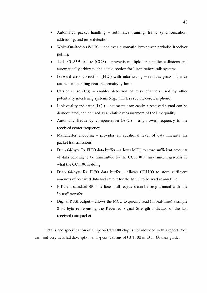
40
• Automated packet handling – automates training, frame synchronization,
addressing, and error detection
• Wake-On-Radio (WOR) – achieves automatic low-power periodic Receiver
polling
• Tx-If-CCA™ feature (CCA) – prevents multiple Transmitter collisions and
automatically arbitrates the data direction for listen-before-talk systems
• Forward error correction (FEC) with interleaving – reduces gross bit error
rate when operating near the sensitivity limit
• Carrier sense (CS) – enables detection of busy channels used by other
potentially interfering systems (e.g., wireless router, cordless phone)
• Link quality indicator (LQI) – estimates how easily a received signal can be
demodulated; can be used as a relative measurement of the link quality
• Automatic frequency compensation (AFC) – align own frequency to the
received center frequency
• Manchester encoding – provides an additional level of data integrity for
packet transmissions
• Deep 64-byte Tx FIFO data buffer – allows MCU to store sufficient amounts
of data pending to be transmitted by the CC1100 at any time, regardless of
what the CC1100 is doing
• Deep 64-byte Rx FIFO data buffer – allows CC1100 to store sufficient
amounts of received data and save it for the MCU to be read at any time
• Efficient standard SPI interface – all registers can be programmed with one
"burst" transfer
• Digital RSSI output – allows the MCU to quickly read (in real-time) a simple
8-bit byte representing the Received Signal Strength Indicator of the last
received data packet
Details and specification of Chipcon CC1100 chip is not included in this report. You
can find very detailed description and specifications of CC1100 in CC1100 user guide.

41
3.3.2. Used Features
In this project, we used CC1100 in 433 MHz frequency band and 250 kbps data rate
with MSK modulation. Also, varieties of features supported by CC1100 are implemented.
CC1100 can be configured to achieve optimum performance for many different
applications. Configuration is done using the SPI interface. The following key parameters
can be programmed:
• Power-down / power up mode
• Crystal oscillator power-up / power-down
• Receive / transmit mode
• RF channel selection
• Data rate
• Modulation format
• RX channel filter bandwidth
• RF output power
• Data buffering with separate 64-byte receive and transmit FIFOs
• Packet radio hardware support
• Forward Error Correction with interleaving
• Data Whitening
• Wake-On-Radio (WOR)
3.3.2.1. Radio State Machine
CC1100 has a built-in state machine that is used to switch between different
operational states (modes). The change of state is done either by using command strobes or
by internal events such as TX FIFO underflow.
The state machine diagram can be founded in CC1100 User Guide.
42
3.3.2.2. Data FIFO
The CC1100 contains two 64 byte FIFOs, one for received data and one for data to
be transmitted. The SPI interface is used to read from the RX FIFO and write to the TX
FIFO. The FIFO controller will detect overflow in the RX FIFO and underflow in the TX
FIFO.
When writing to the TX FIFO it is the responsibility of the MCU to avoid TX FIFO
overflow. A TX FIFO overflow will result in an error in the TX FIFO content. Likewise,
when reading the RX FIFO the MCU must avoid reading the RX FIFO past its empty
value, since an RX FIFO underflow will result in an error in the data read out of the RX
FIFO. The chip status byte that is available on the SO pin while transferring the SPI
address contains the fill grade of the RX FIFO if the address is a read operation and the fill
grade of the TX FIFO if the address is a write operation.
The number of bytes in the RX FIFO and TX FIFO can be read from the status
registers RXBYTES.NUM_RXBYTES and TXBYTES.NUM_TXBYTES respectively. If
a received data byte is written to the RX FIFO at the exact same time as the last byte in the
RX FIFO is read over the SPI interface, the RX FIFO pointer is not properly updated and
the last read byte is duplicated.
3.3.2.3. Packet Format
The CC1100 has built-in hardware support for packet oriented radio protocols. In
transmit mode, the packet handler will add the following elements to the packet stored in
the TX FIFO:
• A programmable number of preamble bytes.
• A two byte synchronization (sync.) word. Can be duplicated to give a 4-byte
sync word (Recommended).
• Optionally whiten the data with a PN9 sequence.
• Optionally Interleave and Forward Error Code the data.
• Optionally compute and add a CRC checksum over the data field.
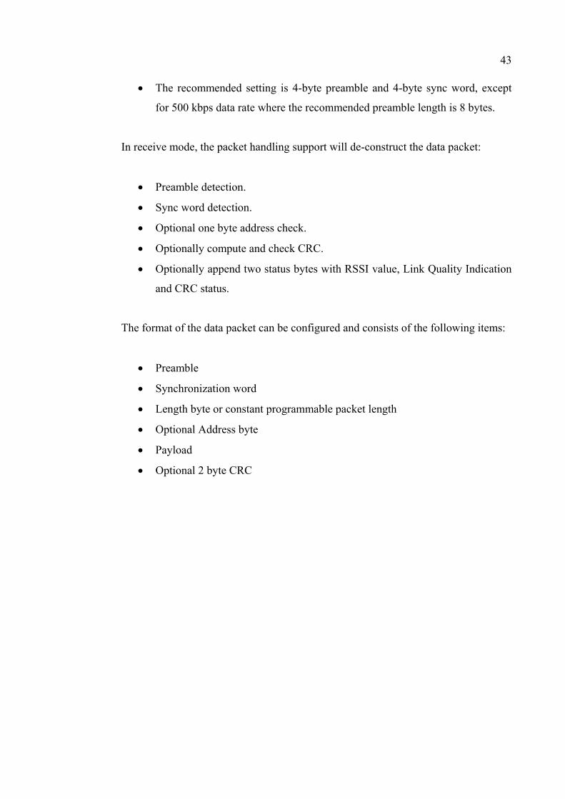
43
• The recommended setting is 4-byte preamble and 4-byte sync word, except
for 500 kbps data rate where the recommended preamble length is 8 bytes.
In receive mode, the packet handling support will de-construct the data packet:
• Preamble detection.
• Sync word detection.
• Optional one byte address check.
• Optionally compute and check CRC.
• Optionally append two status bytes with RSSI value, Link Quality Indication
and CRC status.
The format of the data packet can be configured and consists of the following items:
• Preamble
• Synchronization word
• Length byte or constant programmable packet length
• Optional Address byte
• Payload
• Optional 2 byte CRC
44
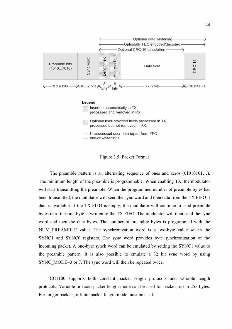
Figure 3.5: Packet Format
The preamble pattern is an alternating sequence of ones and zeros (01010101…).
The minimum length of the preamble is programmable. When enabling TX, the modulator
will start transmitting the preamble. When the programmed number of preamble bytes has
been transmitted, the modulator will send the sync word and then data from the TX FIFO if
data is available. If the TX FIFO is empty, the modulator will continue to send preamble
bytes until the first byte is written to the TX FIFO. The modulator will then send the sync
word and then the data bytes. The number of preamble bytes is programmed with the
NUM_PREAMBLE value. The synchronization word is a two-byte value set in the
SYNC1 and SYNC0 registers. The sync word provides byte synchronization of the
incoming packet. A one-byte synch word can be emulated by setting the SYNC1 value to
the preamble pattern. It is also possible to emulate a 32 bit sync word by using
SYNC_MODE=3 or 7. The sync word will then be repeated twice.
CC1100 supports both constant packet length protocols and variable length
protocols. Variable or fixed packet length mode can be used for packets up to 255 bytes.
For longer packets, infinite packet length mode must be used.
45
3.3.2.4. Wake-on-Radio
The Wake on Radio (WOR) functionality enables CC1100 to periodically wake up
from deep sleep and listen for incoming packets without MCU interaction.
When WOR is enabled, the CC1100 will go to the SLEEP state when CSn is released
after the SWOR command strobe has been sent on the SPI interface. The RC oscillator
must be enabled before the WOR strobe can be used, as it is the clock source for the WOR
timer. The on-chip timer will set CC1100 into IDLE state and then RX state. After a
programmable time in RX, the chip will go back to the SLEEP state, unless a packet is
received.
CC1100 can be set up to signal the MCU that a packet has been received by using the
GDO pins. If a packet is received, the RXOFF_MODE will determine the behavior at the
end of the received packet. When the MCU has read the packet, it can put the chip back
into SLEEP with the SWOR strobe from the IDLE state. The FIFO will loose its contents
in the SLEEP state.
3.3.2.5. Forward Error Correction
CC1100 has built in support for Forward Error Correction (FEC). To enable this
option, set FEC_EN to 1. FEC is only supported in fixed packet length mode
(LENGTH_CONFIG=0). FEC is employed on the data field and CRC word in order to
reduce the gross bit error rate when operating near the sensitivity limit. Redundancy is
added to the transmitted data in such a way that the receiver can restore the original data in
the presence of some bit errors.
The use of FEC allows correct reception at a lower SNR, thus extending
communication range if the receiver bandwidth remains constant. Alternatively, for a given
SNR, using FEC decreases the bit error rate (BER).

46
Finally, in realistic ISM radio environments, transient and time-varying phenomena
will produce occasional errors even in otherwise good reception conditions. FEC will mask
such errors and, combined with interleaving of the coded data, even correct relatively long
periods of faulty reception (burst errors).
The FEC scheme adopted for CC1100 is convolutional coding, in which n bits are
generated based on k input bits and the m most recent input bits, forming a code stream
able to withstand a certain number of bit errors between each coding state (the m-bit
window).
The convolutional coder is a rate 1/2 code with a constraint length of m=4. The coder
codes one input bit and produces two output bits; hence, the effective data rate is halved.
I.e. to transmit the same effective data rate when using FEC, it is necessary to use twice as
high over-the-air data rate. This will require a higher receiver bandwidth, and thus reduce
sensitivity. In other words the improved reception by using FEC and the degraded
sensitivity from a higher receiver bandwidth will be counteracting factors.
3.4. Other Peripheral Components
3.4.1. LCD
LCDs can add a lot to your application in terms of providing an useful interface for
the user, debugging an application or just giving it a "professional" look. The most
common type of LCD controller is the Hitachi 44780 which provides a relatively simple
interface between a processor and an LCD. Using this interface is often not attempted by
inexperienced designers and programmers because it is difficult to find good
documentation on the interface, initializing the interface can be a problem and the displays
themselves are expensive. [15]
47
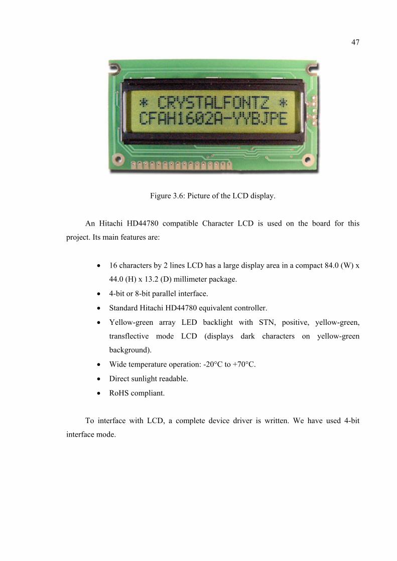
Figure 3.6: Picture of the LCD display.
An Hitachi HD44780 compatible Character LCD is used on the board for this
project. Its main features are:
• 16 characters by 2 lines LCD has a large display area in a compact 84.0 (W) x
44.0 (H) x 13.2 (D) millimeter package.
• 4-bit or 8-bit parallel interface.
• Standard Hitachi HD44780 equivalent controller.
• Yellow-green array LED backlight with STN, positive, yellow-green,
transflective mode LCD (displays dark characters on yellow-green
background).
• Wide temperature operation: -20°C to +70°C.
• Direct sunlight readable.
• RoHS compliant.
To interface with LCD, a complete device driver is written. We have used 4-bit
interface mode.

48
3.4.2. Audio I/O Circuitry
The MSP430F169 has an integrated 12-bit SAR A/D converter, a hardware
multiplier module that allows efficient realization of digital filters, and an integrated 12-bit
D/A converter module. Such a signal chain circuit is shown in Figure 3.2 using the
MSP430F169.
Figure 3.7: Audio Circuitry
In this figure, microphone and speakers are shown. Additionally, we have Audio
jacks connected parallel to both microphone and speaker on the board. This provides us the
option to use this product with headphones.
3.5. Summary of Hardware Features
According to main features of the board and the components on the board, the
hardware has the following features:
• Display 16x2 characters on LCD (with a switch to on/off the backlight).
• Transmit-Receive wireless packets in up to 500 kbps.
• Transmit-Receive messages from UART interface.
• Get audio samples from Microphone and play sound on Speaker.
49
• General purpose 2 buttons and 2 LEDs.
• General purpose 2x8 pin switches.
• MSP430F169 Microcontroller can operate up to 8 MHz.
50
4. SOFTWARE DESCRIPTION
4.1. Description of the Application
I have listed the hardware features briefly on 3.5, and the rest is the software. The
hardware is pretty well featured, and many different applications can be implemented
using this hardware. On the scope of this project, we implemented a wireless entryphone
application. Also, as a by-product, the software can be configured to implement a Walkie-
Talkie type radio communication application. So, this is also implemented.
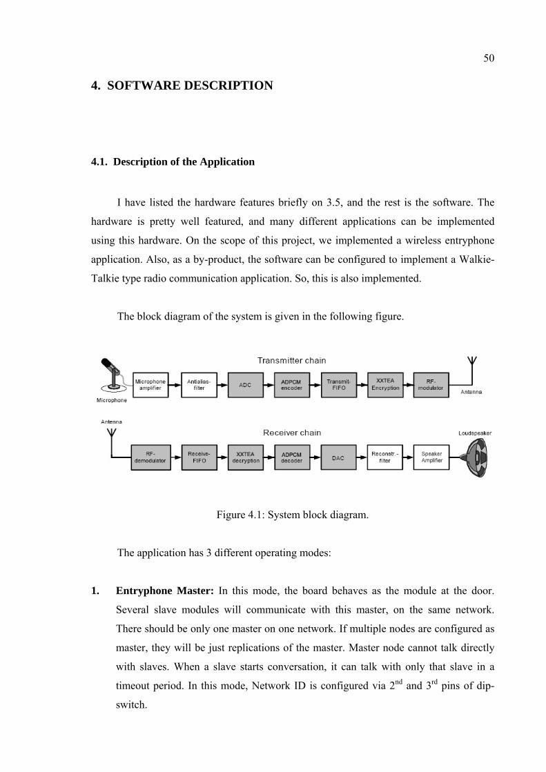
The block diagram of the system is given in the following figure.
Figure 4.1: System block diagram.
The application has 3 different operating modes:
1. Entryphone Master: In this mode, the board behaves as the module at the door.
Several slave modules will communicate with this master, on the same network.
There should be only one master on one network. If multiple nodes are configured as
master, they will be just replications of the master. Master node cannot talk directly
with slaves. When a slave starts conversation, it can talk with only that slave in a
timeout period. In this mode, Network ID is configured via 2nd and 3rd pins of dip-
switch.
51
2. Entryphone Slave: In this mode, the board behaves as the module in each flat, house
or room. Slave nodes can talk directly with master. Each slave mode should have
unique Slave ID. If two or more nodes are configured with same Slave ID, they will
be just replications of each other. Network ID and Slave ID is configured with dip-
switch.
3. Walkie-Talkie Mode: In this mode, the board behaves as a walkie-talkie. The
walkie-talkie devices which are operating in the same channel can talk with each
other directly. The radio channel to operate is configured with dip-switch.
The operating mode can be configured by the rightmost 2 pins of the dip-switch.
4.2. Software State Machine
A very flexible software state machine structure is created as a part of software
architecture of the project. This design provides effortless addition of new states,
modifying existing states and state transition tables, adding / removing something to
application and understanding the application easily.
When the board initialized (i.e. the hardware and MCU is configured), the code goes
into an initial state. Then, every time, the execution is just in one state. State transition can
be indirect call (setting the next state manually), by interrupt (interrupt service routine sets
the next state from state transition table) or directly after one state finishes its execution.
Every state has its corresponding function. This means, when board enters on this
state, this function will be called. This function will call other functions or subroutines,
enable / disable interrupts or changes the state. After the end of execution, code decides the
next state by first the state that is set by current state indirectly, if not, by state transition
table. CPU always sleeps between state transitions. For example, if one state finishes its
code execution and the state transition is going to be fired by an interrupt, CPU is set to
sleep and low power mode. This also provides ultra-low power application.
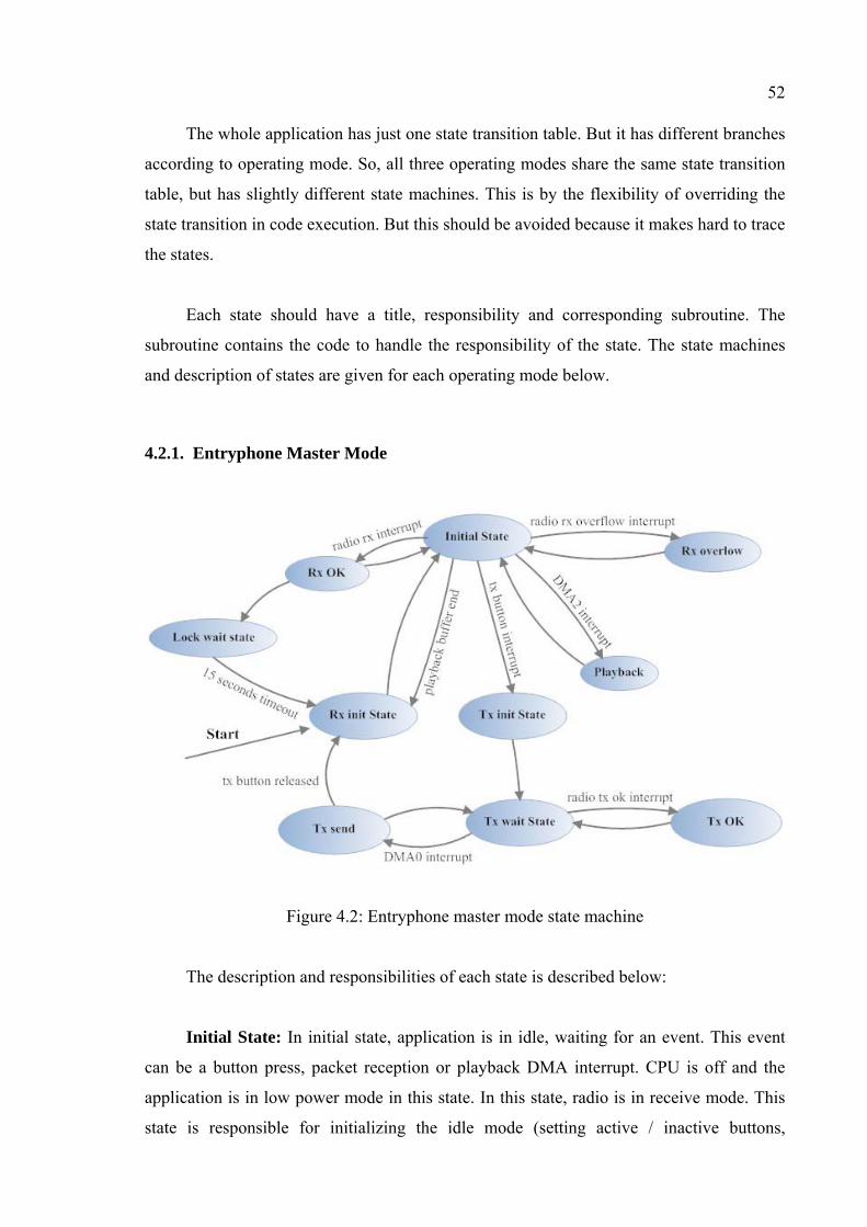
52
The whole application has just one state transition table. But it has different branches
according to operating mode. So, all three operating modes share the same state transition
table, but has slightly different state machines. This is by the flexibility of overriding the
state transition in code execution. But this should be avoided because it makes hard to trace
the states.
Each state should have a title, responsibility and corresponding subroutine. The
subroutine contains the code to handle the responsibility of the state. The state machines
and description of states are given for each operating mode below.
4.2.1. Entryphone Master Mode
Figure 4.2: Entryphone master mode state machine
The description and responsibilities of each state is described below:
Initial State: In initial state, application is in idle, waiting for an event. This event
can be a button press, packet reception or playback DMA interrupt. CPU is off and the
application is in low power mode in this state. In this state, radio is in receive mode. This
state is responsible for initializing the idle mode (setting active / inactive buttons,
53
initializing the encoder etc.), getting ready for both tx and rx and displaying the message
about the current state to user.
Initial state is actually designed for the start state, but since Rx mode initialization is
done in Rx init state, Rx init is the start state.
Rx Init State: This state is responsible for stopping the peripherals (that probably
activated in tx mode), flushing the buffer, initializing radio rx mode and activating the
peripherals that is going to be used in reception (in playback).
After this state, execution immediately switches to initial state.
Tx Init State: This state is responsible for stopping the playback DMA, initializing
radio to tx state and starting sampling. In this state, the tx process is started. This state
starts the sampling timer and changes the state to tx wait state. After this state, received
packets will be ignored.
Tx Wait State: This state is just a dummy state with nothing to do. In this state, tx
mode is already initialized and sampling timer is started. So, this state waits for sampling
interrupt, and when an interrupt comes, it changes the state to tx send state, which will
packetize the data and send over the air. This state is also waits for the tx ok interrupts and
switches to corresponding state, that is tx ok state.
Tx OK State: This state handles the tx ok interrupts and executes the desired code
(notifying the user etc.) This state is not a subroutine, and not exists in state table, this state
is handled by ISR, because it is interrupt specific.
Tx Send State: This state is called when necessary samples are taken by ADC and
DMA to packetize. So, this state is responsible for packaging the information and sending
the packet over air. This state encodes the samples, encrypts the packet and assembles
other contents of the packet, then calls sendPacket() routine.
54
This state also checks the user releases the tx button or not. If the user releases the
button, the packet is not generated and sent, instead, the state is changed to rx init state
which indicated the end of tx session.
Rx overflow State: This state handles the rx overflow interrupt. When it is called,
this state flushes the RX FIFO and buffer, and then returns the radio to rx state. This state
is not a subroutine, and not exists in state table, this state is handled by ISR, because it is
interrupt specific.
Playback State: This state handles the Playback DMA interrupt. When it is called,
this state swaps the buffer and restarts the DMA. So, the playback is continuously running.
This state is not a subroutine, and not exists in state table, this state is handled by ISR,
because it is interrupt specific.
Rx OK State: This state is called from initial state when radio receives a packet.
This state is also called by interrupt and not exists is state transition table. This state is
responsible for checking the incoming packet. This state is one of the different states for
different operating modes. Commonly, this state checks if the packet is a valid packet, then
decrypts it, decodes it, switches the buffer and writes the contents to buffer. In Entryphone
master mode, this state gets the packet, records the sender (for answering) and starts the
playback timer. So, if the packet is valid, the packet is immediately starts to play on
speaker.
Lock wait State: This state has completely different behavior between different
modes. In Entryphone master mode, this state is called just after the packet reception. In
this state, a timer is started. In the timer period, the master mode sees the senders ID in the
LCD and it is allowed to answer to the sender. After the timeout, state is changed to rx init
state and master goes into idle mode.

55
4.2.2. Entryphone Slave Mode
The state machine in this mode is just slightly different than master mode. In the
state perspective the only difference is lock wait state transition and behavior.
Figure 4.3: Entryphone slave mode state machine.
All states are same as the states in master mode, except Rx OK and lock wait states.
Rx OK State: The difference from master mode is, this state calls lock wait state in
master mode by default. But in slave mode, this states calls lock wait state when it sees the
received packet is not belongs to current node. I.e. someone is talking to master mode, so,
the line is busy. The line busy stuff is handled by lock wait state.
Lock wait State: In Entryphone slave mode, this state is called just after when a
different targeted packet than current node is received. In this state, software disables the tx
button, because the line is busy, someone is talking to master. And a timer is started. Timer
is restarted after each packet reception. After the timeout occurs, the board returns to initial
state and tx button is re-enabled.
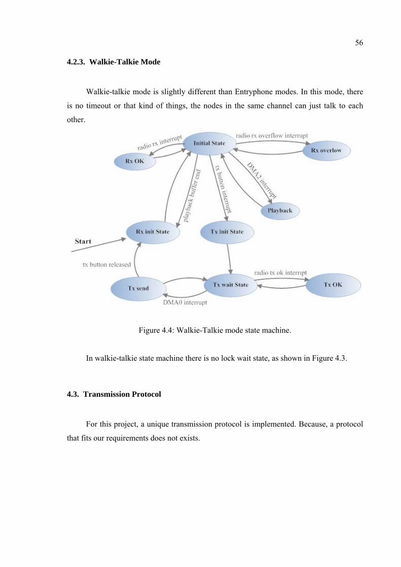
56
4.2.3. Walkie-Talkie Mode
Walkie-talkie mode is slightly different than Entryphone modes. In this mode, there
is no timeout or that kind of things, the nodes in the same channel can just talk to each
other.
Figure 4.4: Walkie-Talkie mode state machine.
In walkie-talkie state machine there is no lock wait state, as shown in Figure 4.3.
4.3. Transmission Protocol
For this project, a unique transmission protocol is implemented. Because, a protocol
that fits our requirements does not exists.
57
Our requirements are as follows:
• Multiple nodes should be able to share the same channel.
• We need to have a continuous real-time sound data transfer. (Guaranteed data
rate)
• Each node should be able to identify the source and destination of the packet,
when they receive a packet.
• Each node should be able to check if a correct packet for this protocol is
received or not.
• No acknowledgement mechanism or RTS / CTS mechanism.
All modes are using the same protocol. But in walkie-talkie mode, there is no need
for actual protocol. In this mode, source and destination address of a packet is not checked.
So, the following scenario is for Entryphone mode.
4.3.1. Basic Transmission Scenario
When the channel is idle, all the slave nodes are in idle state. If a slave node starts to
transmit a packet, or if master node answers to a request, other nodes should be able to
detect this conversation and take themselves in lock wait state. In lock wait state, they are
not allowed to transmit any packet.
The basic assumption in here is that, all nodes are hearing all others. So, the
problems like hidden-node problem do not exist.
When a slave node wants to transmit, it will transmit the audio data continuously.
Slave mode starts to transmit packets with specifying its device id as source address and
master node’s address as destination. Master node’s address is globally and statically
defined in the software and cannot be changed. After the master mode receives a packet, it
checks the packet and records the source address, because it is needed if the master wants
to answer to that message. Other nodes than master mode also receives these packets and
takes them into lock wait state.
58
When slave ends the transmission, it just goes into idle mode, and master node goes
into lock wait state, that it can answer this message in a predefined time period. If, in this
period, master decides to answer, it sends the answer with just specifying its address as
source and the address of the corresponding node (that it was recorded after the last
received packet) as destination. Master can send as many packets or messages as it want in
the lock wait timeout period.
Every node also receives these packets, but only the corresponding node plays this
message. Others will update the timer and stay in lock wait state.
So, a basic conversation is like this. After the timeout, all slaves will get out of lock
wait state and go into idle state.
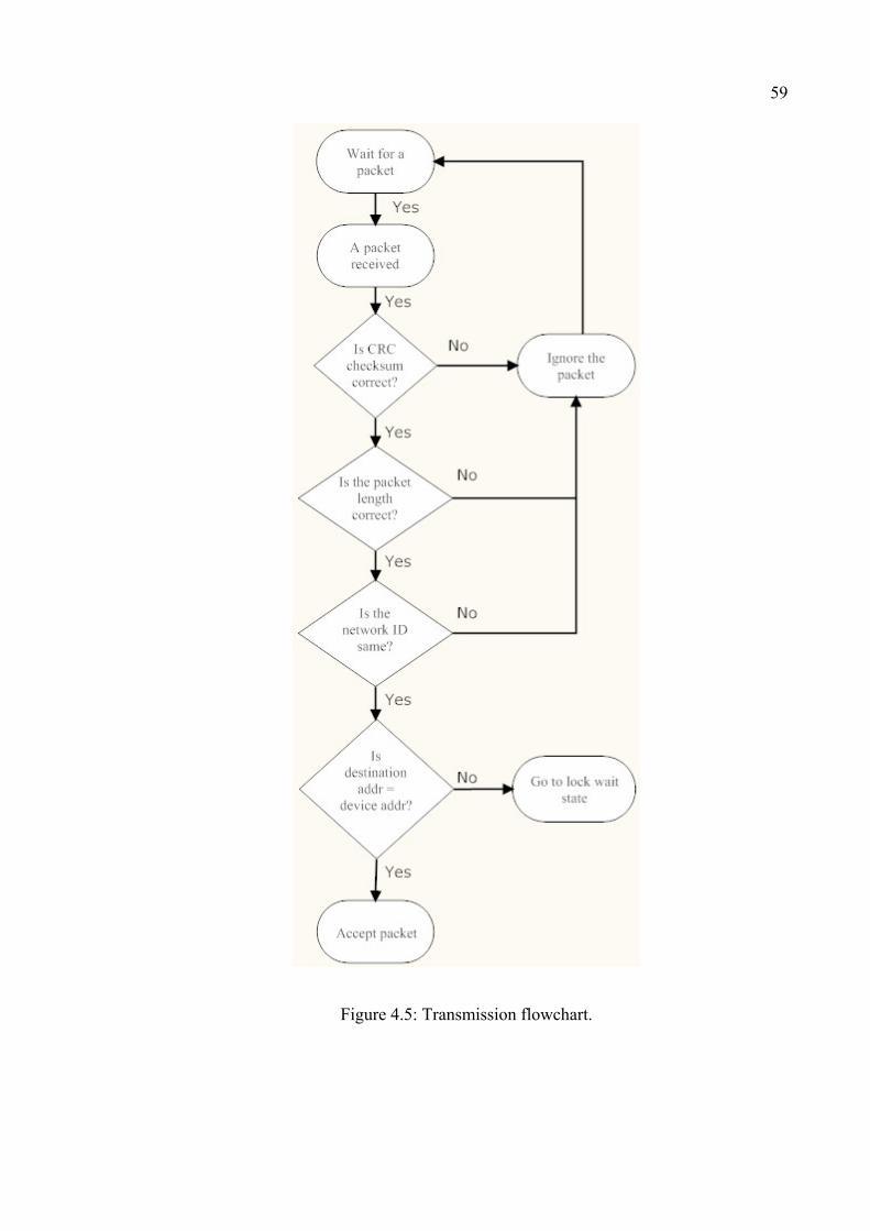
59
Figure 4.5: Transmission flowchart.
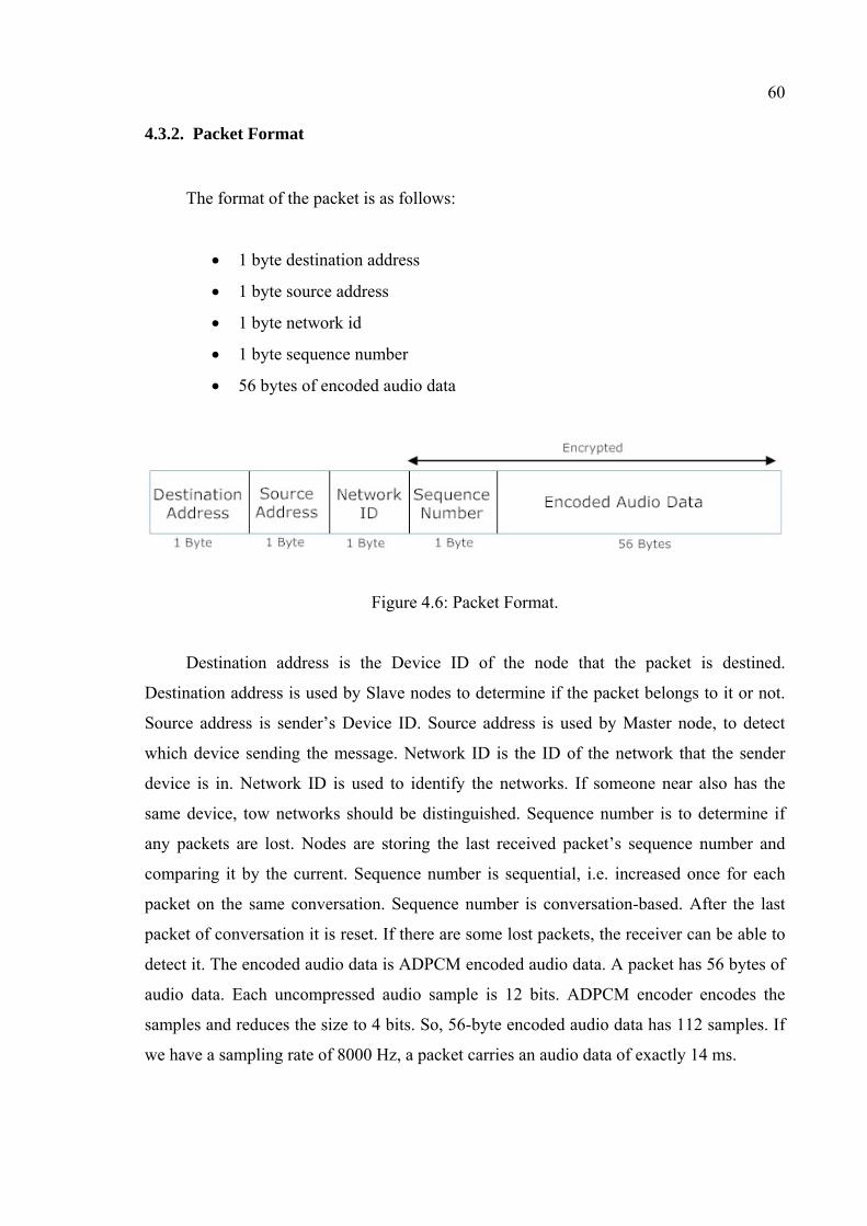
60
4.3.2. Packet Format
The format of the packet is as follows:
• 1 byte destination address
• 1 byte source address
• 1 byte network id
• 1 byte sequence number
• 56 bytes of encoded audio data
Figure 4.6: Packet Format.
Destination address is the Device ID of the node that the packet is destined.
Destination address is used by Slave nodes to determine if the packet belongs to it or not.
Source address is sender’s Device ID. Source address is used by Master node, to detect
which device sending the message. Network ID is the ID of the network that the sender
device is in. Network ID is used to identify the networks. If someone near also has the
same device, tow networks should be distinguished. Sequence number is to determine if
any packets are lost. Nodes are storing the last received packet’s sequence number and
comparing it by the current. Sequence number is sequential, i.e. increased once for each
packet on the same conversation. Sequence number is conversation-based. After the last
packet of conversation it is reset. If there are some lost packets, the receiver can be able to
detect it. The encoded audio data is ADPCM encoded audio data. A packet has 56 bytes of
audio data. Each uncompressed audio sample is 12 bits. ADPCM encoder encodes the
samples and reduces the size to 4 bits. So, 56-byte encoded audio data has 112 samples. If
we have a sampling rate of 8000 Hz, a packet carries an audio data of exactly 14 ms.
61
4.3.3. Transmission / Data Rate Requirements
As previously calculated, a packet contains 14 ms of audio samples. That means, we
have to deliver or receive and process each packet in 14 ms, for continuous voice
transmission.
We have a packet of 60 bytes. But this packet is transmission protocol’s packet. This
is the payload of the packet transmitted over the air. The transmitted packet has additional
overhead. The exact packet format that is transmitted over the air is described in section
3.3.2.3.
We have used 64 bit preamble, 32 bit sync word and 16 bit CRC. We also used FEC
encoding, which means doubling the size of encoded part.
After all, the transmitted packet over the air is 128 bytes. Since we have to send a
packet per 14 ms, the minimum required data rate is approximately 71.43 kilobits per
second in theory. In practice, since we need additional time to sample, assemble, encrypt
and encode the packet in transmitted side and decrypt, decode and play the packet in
receiver side, we used the radio in 250 kbits/s mode. But minimum, 100 kbits/s can be
used.
The time chart including each operation is described in Section 5.3.
4.4. Device Driver Implementations
In this project, we used various peripherals of MSP430 microcontroller. We also
used external components like radio chip or LCD. To use them, device drivers of most of
the modules of MSP430 and device drivers of external components are needed. Some
hardware abstraction library is provided by vendor, but most of them are re-written as a
part of this project.
The idea of a hardware abstraction layer (HAL) is to provide a standard interface to
hardware resources on any board.
62
The common part of the HAL contains the core functionality of the library, that is the
functions for accessing the CC1100 and the CC2500 using the SPI interface. The common
part can be reused on any MSP430 based target board.
The target specific part of the HAL is necessary in order to configure the MCU – it
sets up the clock system, configures I/O pins for general purpose use and dedicated
peripherals etc. In addition, it contains functions for accessing target or board specific
units, such as UART, LCD and LEDs.
This section describes the brief specification and properties of the device drivers that
are implemented as a part of this project.
4.4.1. DMA Controller
The DMA Module of MSP430 is used for data transmission from ADC and to DAC
modules of MSP430. DMA module is also used for UART transmission. DMA module is
very useful because it can transfer data from / to various peripherals with zero CPU
interruption.
The DMA controller module of MSP430F169 has 3 independent channels. For more
information about DMA module, please refer to User Guide of MSP430.
The device driver is completely implemented as a part of this project. With the
implemented device driver, each channel can be easily configured, initialized or disabled.
Also, interrupt handlers for each channel can be easily configured and can be automatically
assigned to any function or subroutine.
4.4.2. Timer Module
MSP430F169 has two timer modules. Timer modules can be used to generate an
interrupt after a specific timeout, or capture the current counter in the timer. For more
information about Timer module, please refer to User Guide of MSP430.
63
Timer modules are used to generate the sampling frequency and generating the
timeout of lock wait state in Entryphone mode.
The device driver of timer module is enhanced and changed due to the changes on
the board, with using the hardware abstraction library that is provided by the vendor. The
implemented driver is capable of generating PWM signals, setting/resetting timer and
easily connect / handle the interrupt.
4.4.3. USART Peripheral Interface
The MSP430F169 Microcontroller has two USART modules, each is capable of
working on UART, SPI or I2C modes. For more information about USART modules,
please refer to User Guide of MSP430.
In this project SPI is used to interface with Wireless Module, and UART is used to
print debug output to PC on RS-232 serial console. The SPI device driver is supplied by
TI, but the UART mode driver is completely written as a part of this project.
The implemented UART driver is capable of printing a string, integer or hex to
console easily. The reading part is not implemented, but the prototypes are added. The
driver supports automatic configuration and initialization in baud rates of 9600 with 32k
crystal and 115200 with 8 MHz crystal. The operation is very fast, and the driver is
integrated with DMA driver, and it is possible to select the use of DMA when transmitting
a long data with zero CPU interruption.
4.4.4. ADC Module
The Analog-to-Digital converter (ADC) module of MSP430 is capable of taking
samples in various modes and various speeds with using multiple channels. For more
information, you can refer to family user guide of MSP430.
64
There was no HAL code provided by the vendor about ADC module, so, all driver is
written as a part of this project.
The implemented driver is capable of easily configuring the ADC module, starting-
stopping sampling and adjusting sampling and timing source. It can also be easily
integrated with DMA module.
4.4.5. DAC Module
MSP430 also has a very powerful Digital-to-Analog converter module. For more
information, you can refer to family user guide of MSP430.
This module is used to drive the audio output and playback the received audio data.
Since it is heavily used in the project, a simple device driver is implemented as a part of
this project, because there was no code provided by TI.
The driver can easily configure, start and stop the DAC with various modes. DAC
module is used with DMA in the project. The interrupts of DAC is automatically handled
by DMA, and the interrupts of DMA is handled by the application.
4.5. Buffering Mechanism
In computing, a buffer is a region of memory used to temporarily hold data while it is
being moved from one place to another. Typically, the data is stored in a buffer as it is
retrieved from an input device (such as a keyboard) or just before it is sent to an output
device (such as a printer). However, a buffer may be used when moving data between
processes within a computer. This is comparable to buffers in telecommunication. Buffers
can be implemented in either hardware or software, but the vast majority of buffers are
implemented in software. Buffers are typically used when there is a difference between the
rate at which data is received and the rate at which it can be processed, or in the case that
these rates are variable, for example in a printer spooler.
65
In telecommunication, a buffer is a routine or storage medium used in
telecommunications to compensate for a difference in rate of flow of data, or time of
occurrence of events, when transferring data from one device to another. The main purpose
of buffer usage is to allow timing corrections to be made on a data stream.
In this project, we used a circular buffer structure. A circular buffer or ring buffer is a
data structure that uses a single, fixed-size buffer as if it were connected end-to-end. This
structure lends itself easily to buffering data streams.
There are two pointers that point on the buffer: First one is for playback. Playback
buffer pointer points to the current position to be played. Second pointer is the next buffer
pointer to write incoming data. Two pointers are independent, and consumer (playback)
and producer (writing to buffer) accesses the buffer independently. Controlling the buffer
access is done by setting a “used” bit to each buffer space.
The buffer system is illustrated in following figure.
Figure 4.7: Circular buffer structure.
The number of elements in the buffer is easily configured in the code. Note that,
there should be at least 3 elements in the buffer to compensate possible delays in air and
provide clear sound. The number of elements will be increased to compensate more packet

66
losses. But increased number of elements will cause delay in the sound, because half of the
elements should be filled to start playback. Measurements show that, in practical, 5
elements is the optimum for balanced delay and loss compensation.
Each element in the buffer contains decrypted, decoded and uncompressed audio
data, ready to play on DAC. The playback process is fired when the half of the circular
buffer is filled.
The code written to ensure this buffering mechanism provides easy swapping,
flushing or filling the buffer and auto-checking any possible buffer overrun case.
4.6. Audio Compression and Voice Encoding / Decoding
4.6.1. Sampling Theory and Implementation
In signal processing, sampling is the reduction of a continuous signal to a discrete
signal. A common example is the conversion of a sound wave (a continuous-time signal) to
a sequence of samples (a discrete-time signal). A sample refers to a value or set of values
at a point in time and/or space.
A sampler is a subsystem or operator that extracts samples from continuous signal. A
theoretical ideal sampler multiplies a continuous signal with a Dirac comb. This
multiplication "picks out" values but the result is still continuous-valued. If this signal is
then discretized (i.e., converted into a sequence) and quantized along all dimensions it
becomes a discrete signal.
A partial answer to the question “Under what circumstances is it possible to
reconstruct the original signal completely?” is provided by the Nyquist–Shannon sampling
theorem, which provides a sufficient (but not always necessary) condition under which
perfect reconstruction is possible. The sampling theorem guarantees that bandlimited
signals (i.e., signals which have a maximum frequency) can be reconstructed perfectly
from their sampled version, if the sampling rate is more than twice the maximum

67
frequency. Reconstruction in this case can be achieved using the Whittaker–Shannon
interpolation formula. [16]
The frequency equal to one-half of the sampling rate is therefore a bound on the
highest frequency that can be unambiguously represented by the sampled signal. This
frequency (half the sampling rate) is called the Nyquist frequency of the sampling system.
Frequencies above the Nyquist frequency fN can be observed in the sampled signal, but
their frequency is ambiguous. That is, a frequency component with frequency f cannot be
distinguished from other components with frequencies NfN + f and NfN – f for nonzero
integers N. This ambiguity is called aliasing. To handle this problem as gracefully as
possible, most analog signals are filtered with an anti-aliasing filter (usually a low-pass
filter with cutoff near the Nyquist frequency) before conversion to the sampled discrete
representation.
A more general statement of the Nyquist–Shannon sampling theorem says more or
less that the signals with frequencies higher than the Nyquist frequency can be sampled
without loss of information, provided their bandwidth (non-zero frequency band) is small
enough to avoid ambiguity, and the bandlimits are known.
In practice, the continuous signal is sampled using an analog-to-digital converter
(ADC), a non-ideal device with various physical limitations. This results in deviations
from the theoretically perfect reconstruction capabilities, collectively referred to as
distortion.
When it is necessary to capture audio covering the entire 20–20,000 Hz range of
human hearing, such as when recording music or many types of acoustic events, audio
waveforms are typically sampled at 44.1 kHz (CD) or 48 kHz (professional audio). The
approximately double-rate requirement is a consequence of the Nyquist theorem.
Speech signals, i.e., signals intended to carry only human speech can usually be
sampled at a much lower rate. For most phonemes, almost all of the energy is contained in
the 5Hz-4 kHz range, allowing a sampling rate of 8 kHz. This is the sampling rate used by
nearly all telephony systems, which use the G.711 sampling and quantization
specifications. In this project, we used a sample rate of 8 kHz.

68
4.6.2. The ADPCM Codec
Adaptive PCM or ADPCM is a further development of DPCM where the quantizer
and/or the predictor is adaptive. This means they are adjusted according to the nature of the
input signal. If the input signal is small, the quantizer steps are small, if the input signal is
large, the quantizer steps are large. This gives less error than the fixed nonlinear quantizer
and the low, constant bitrate can be maintained. For more information about DPCM and
ADPCM, please refer to Appendix A of this report.
4.6.2.1. Implementation
ADPCM is very widespread in telephone communications and speech coding and
many different algorithms exist. The Interactive Multimedia Association (IMA)
recommended a standard for ADPCM-codec in multimedia applications, known as IMA or
DVI ADPCM, in the early 1990s. This algorithm is now used in most cross-platform
ADPCM-based audio applications. In this report, a general explanation of the concepts
behind ADPCM will be given in Appendix A, while any specifics will be in accordance
with the IMA-standard.
Embedded adaptive differential pulse coded modulation (ADPCM) algorithms
quantize the difference between the input signal and the estimated signal into core bits and
enhancement bits. This feature gives them an advantage over non-embedded algorithms
because they allow an intermediate node to drop the enhancement bits without having to
exchange control messages with the transmitting end. [17]
The proposed IMA-standard, now widely used in multimedia applications, uses an
adaptive quantizer, but a fixed predictor to limit the computational complexity. The
predictor is identical to the one in the DPCM. The compression level is 4:1, which means
the 16-bit original signal is quantized to 4-bits. The stepsize of the quantization depends on
the input signal, thus making it adaptive. The adaptation is based on the current stepsize
and the quantizer output of the immediately previous input. This adaptation is done as a
sequence of two table lookups. The three bits representing the number of quantizer levels
serve as an index into the first table lookup whose output is an index adjustment for the
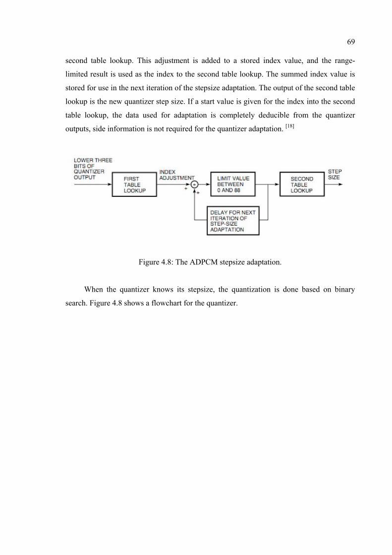
69
second table lookup. This adjustment is added to a stored index value, and the range-
limited result is used as the index to the second table lookup. The summed index value is
stored for use in the next iteration of the stepsize adaptation. The output of the second table
lookup is the new quantizer step size. If a start value is given for the index into the second
table lookup, the data used for adaptation is completely deducible from the quantizer
outputs, side information is not required for the quantizer adaptation. [18]
Figure 4.8: The ADPCM stepsize adaptation.
When the quantizer knows its stepsize, the quantization is done based on binary
search. Figure 4.8 shows a flowchart for the quantizer.
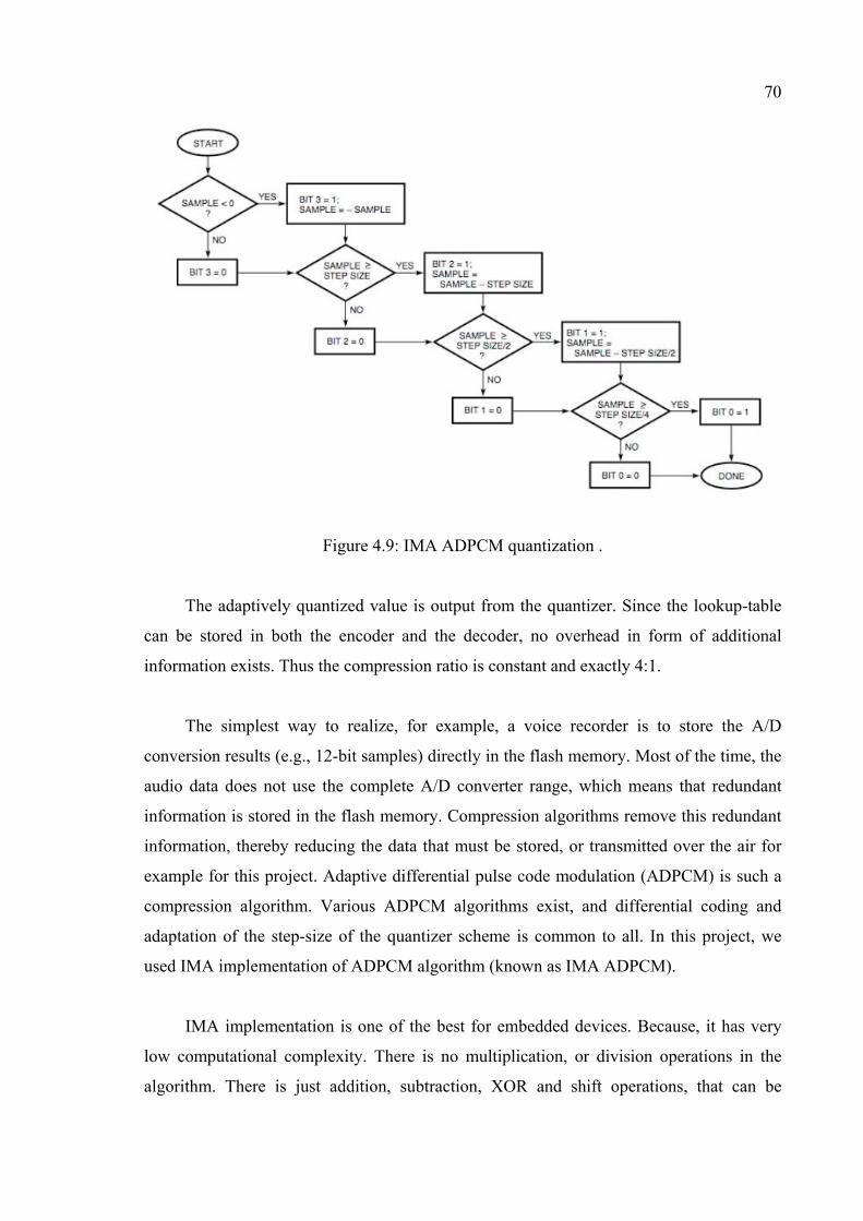
70
Figure 4.9: IMA ADPCM quantization .
The adaptively quantized value is output from the quantizer. Since the lookup-table
can be stored in both the encoder and the decoder, no overhead in form of additional
information exists. Thus the compression ratio is constant and exactly 4:1.
The simplest way to realize, for example, a voice recorder is to store the A/D
conversion results (e.g., 12-bit samples) directly in the flash memory. Most of the time, the
audio data does not use the complete A/D converter range, which means that redundant
information is stored in the flash memory. Compression algorithms remove this redundant
information, thereby reducing the data that must be stored, or transmitted over the air for
example for this project. Adaptive differential pulse code modulation (ADPCM) is such a
compression algorithm. Various ADPCM algorithms exist, and differential coding and
adaptation of the step-size of the quantizer scheme is common to all. In this project, we
used IMA implementation of ADPCM algorithm (known as IMA ADPCM).
IMA implementation is one of the best for embedded devices. Because, it has very
low computational complexity. There is no multiplication, or division operations in the
algorithm. There is just addition, subtraction, XOR and shift operations, that can be
71
executed very fast on ALU. Also, IMA implementation has small codesize and memory
usage.
More information and analysis about code size and CPU usage is done in analysis
section.
4.7. Security Implementation and Encryption
Wireless networking is revolutionizing the way people work and play. By removing
physical constraints commonly associated with high-speed networking, individuals are able
to use networks in ways never possible in the past. Students can be connected to the
Internet from anywhere on campus. Family members can check email from anywhere in a
house. Neighbors can pool resources and share one high-speed Internet connection. Over
the past several years, the price of wireless networking equipment has dropped
significantly.
Unfortunately, wireless networking is a double-edged sword. Wireless users have
many more opportunities in front of them, but those opportunities open up the user to
greater risk. The risk model of network security has been firmly entrenched in the concept
that the physical layer is at least somewhat secure. With wireless networking, there is no
physical security. The radio waves that make wireless networking possible are also what
make wireless networking so dangerous. An attacker can be anywhere nearby listening to
all the traffic from your network in your yard, in the parking lot across the street, or on the
hill outside of town. By properly engineering and using your wireless network, you can
keep attackers at bay.
4.7.1. Attacks and Risks
Wireless networks cannot be physically secured the same way a wired network can
be. An attack against a wireless network can take place anywhere: from the next office, the
parking lot of your building, across the street in the park, or a bluff many miles away.
72
Understanding the details of various attacks against your wireless infrastructure is
critical to determining how to defend. Some attacks are easy to implement but aren't
particularly dangerous. Other attacks are much more difficult to mount but can be
devastating. Like any other aspect of security, wireless security is a game of risk. By
knowing the risks involved in your network and making informed decisions about security
measures, you have a better chance at protecting yourself, your assets, and your users.
The risks to users of wireless technology have increased as the service has become
more popular. There were relatively few dangers when wireless technology was first
introduced. Crackers had not yet had time to latch on to the new technology and wireless
was not commonly found in the work place. However, there are a great number of security
risks associated with the current wireless protocols and encryption methods, and in the
carelessness and ignorance that exists at the user and corporate IT level. Cracking methods
have become much more sophisticated and innovative with wireless. Cracking has also
become much easier and more accessible with easy-to-use Windows-based and Linux-
based tools being made available on the web at no charge.
For this project, although the transmitted information (voice) is not very security
critical, a simple symmetric encryption algorithm is implemented and used. Thus, nobody
except the nodes in the same network can easily capture and see the contents of the
packets.
4.7.2. Tiny Encryption Algorithm and Variants
The Tiny Encryption Algorithm (TEA) is a block cipher notable for its simplicity of
description and implementation (typically a few lines of code). It was designed by David
Wheeler and Roger Needham of the Cambridge Computer Laboratory, and first presented
at the Fast Software Encryption workshop in 1994. The cipher is not subject to any patents.
The first published version of TEA was supplemented by a second version which
incorporated extensions to TEA to make it more secure. 'Block TEA' (sometimes referred
to as XTEA), operates on arbitrary-size blocks in place of the 64-bit blocks of the original.
73
A third version (XXTEA), published in 1998, described Corrections to xtea to
enhance the security of the Block TEA algorithm.
The history, description, cryptanalysis and details of TEA, XTEA and XXTEA are
covered in Appendix B in more details. In this section, we will deal with implementation
and benefits.
4.7.2.1. Implementation
In this project, we implemented an optimized version on XXTEA. TEA is preferred
because of its simple implementation and requires very low computational power. So, it is
very fast.
Executing encryption software on a microcontroller is a fine balance between
security level, size, and cycles. In general, the more secure an algorithm, the more cycles
that are required. The XXTEA was chosen because it offers the best security-to-cycles
ratio. As written, it does 32 iterations, with any single bit change in the input data being
fully propagated in 4 iterations. The security is similar to DES, but it is done with one-third
the cycles of DES. This is accomplished by using less-complicated equations but executing
more iterations. It was designed for a small memory footprint and low MIPS requirement.
Instead of using a complex mathematical formula for encryption, TEA relies on a simple
formula with many iterations.
Our implementation has 128-bit hard coded key, and 56 bytes of blocks. So, each
packet is a block. XXTEA provides configurable block size in multiplies of 64-bits.
Encryption and Decryption is made by the same routine. Decryption is just the
reverse of encryption, and has nearly the same computational complexity. Analysis of the
computational power, time and memory requirements are done in analysis section.

74
4.7.2.2. Key Features & Benefits
The key features and benefits of XXTEA contain:
• 128-bit key.
• Multiples of 32-bit block size (Minimum 64 bit)
• Very low computational power and memory requirements.
• Offers the best security-to-cycles ratio
• Easy to implement.
• Provides good security in much less cycles.
• More efficient for longer messages.
• Publicly available, no patent or license issues.

75
5. ANALYSIS
Analysis is an important part of a report, especially for embedded hardware or
software design. Because, embedded devices has more limited computation power, storage
space, memory or input power limitations than regular devices.
In the scope of this report, Memory, CPU time and power analysis is done. Memory
and CPU requirements are analyzed with IAR’s Embedded Workbench software.
IAR Embedded Workbench software provides a very good compiler, debugger
interface and simulator for MSP430 and many other popular microcontrollers.
Note that, the implemented code has a modular design, so you can select the
specification of the device in compile time. For example, you can specify LCD Module
support, UART support and Encryption support when compiling the software. The analysis
is done for each specific software module.
Power consumption requirements are taken from specific devices’ data sheets.
5.1. Memory Usage / Requirements
According to linker output of IAR Compiler, the memory requirements are shown
into following tables.
Table 5.1: Memory usage of whole code.
Code Memory Data Memory Constant Memory
No Optimization 9,256 bytes 1,683 bytes 1,030 bytes Code Size Optimized 7,502 bytes 1,683 bytes 1,029 bytes Speed Optimized 8,888 bytes 1,683 bytes 1,029 bytes
Balanced Optimization 7,906 bytes 1,683 bytes 1,029 bytes
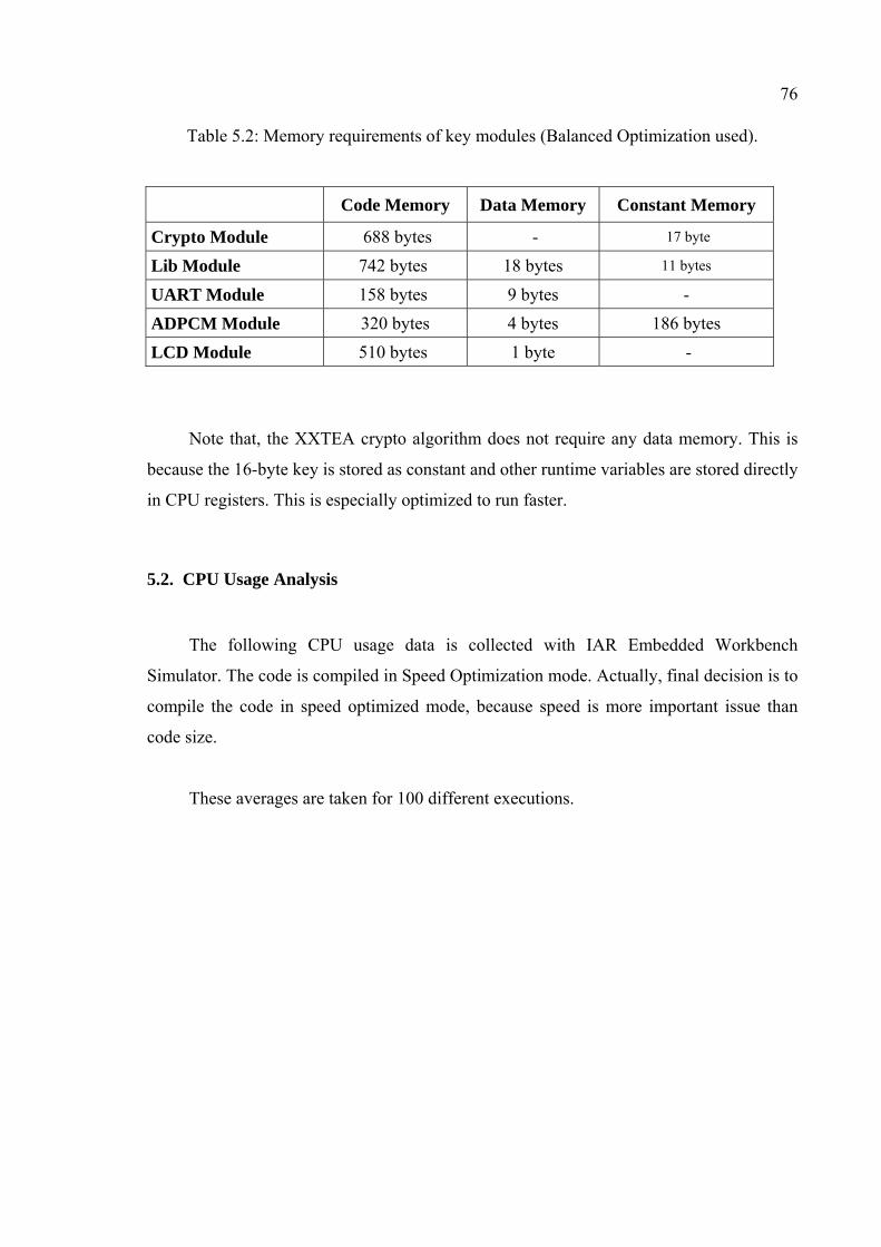
76
Table 5.2: Memory requirements of key modules (Balanced Optimization used).
Code Memory Data Memory Constant Memory
Crypto Module 688 bytes - 17 byte
Lib Module 742 bytes 18 bytes 11 bytes
UART Module 158 bytes 9 bytes - ADPCM Module 320 bytes 4 bytes 186 bytes LCD Module 510 bytes 1 byte -
Note that, the XXTEA crypto algorithm does not require any data memory. This is
because the 16-byte key is stored as constant and other runtime variables are stored directly
in CPU registers. This is especially optimized to run faster.
5.2. CPU Usage Analysis
The following CPU usage data is collected with IAR Embedded Workbench
Simulator. The code is compiled in Speed Optimization mode. Actually, final decision is to
compile the code in speed optimized mode, because speed is more important issue than
code size.
These averages are taken for 100 different executions.
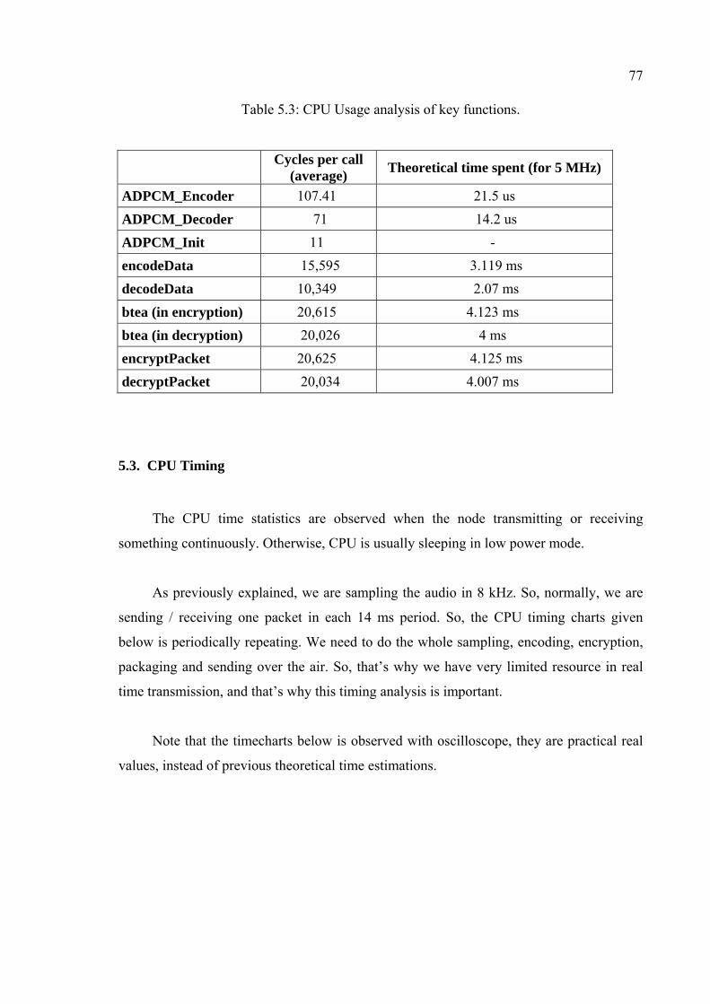
77
Table 5.3: CPU Usage analysis of key functions.
Cycles per call (average) Theoretical time spent (for 5 MHz)
ADPCM_Encoder 107.41 21.5 us ADPCM_Decoder 71 14.2 us ADPCM_Init 11 - encodeData 15,595 3.119 ms decodeData 10,349 2.07 ms btea (in encryption) 20,615 4.123 ms btea (in decryption) 20,026 4 ms encryptPacket 20,625 4.125 ms decryptPacket 20,034 4.007 ms
5.3. CPU Timing
The CPU time statistics are observed when the node transmitting or receiving
something continuously. Otherwise, CPU is usually sleeping in low power mode.
As previously explained, we are sampling the audio in 8 kHz. So, normally, we are
sending / receiving one packet in each 14 ms period. So, the CPU timing charts given
below is periodically repeating. We need to do the whole sampling, encoding, encryption,
packaging and sending over the air. So, that’s why we have very limited resource in real
time transmission, and that’s why this timing analysis is important.
Note that the timecharts below is observed with oscilloscope, they are practical real
values, instead of previous theoretical time estimations.
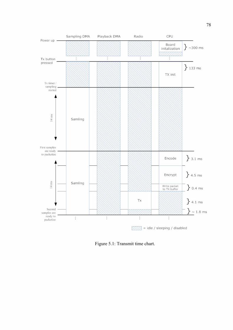
78
Figure 5.1: Transmit time chart.
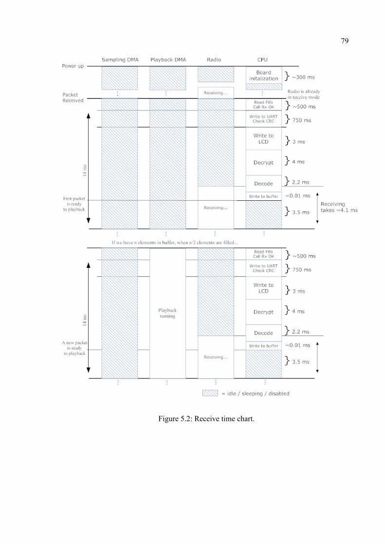
79
Figure 5.2: Receive time chart.
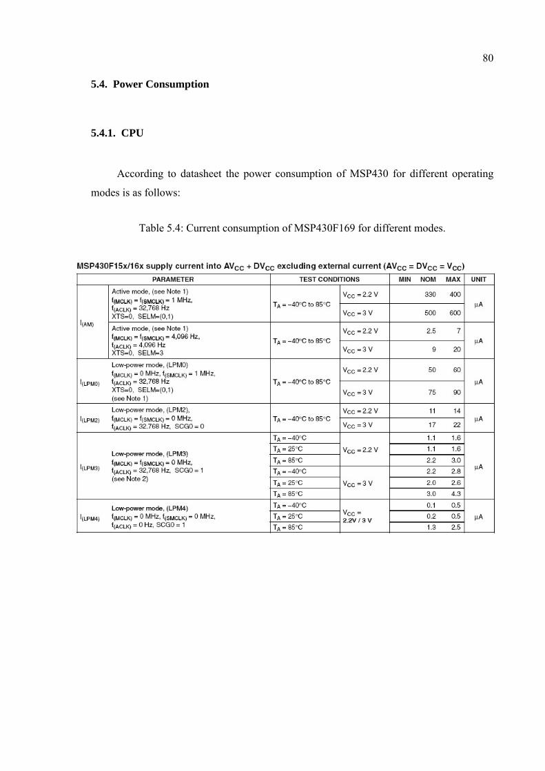
80
5.4. Power Consumption
5.4.1. CPU
According to datasheet the power consumption of MSP430 for different operating
modes is as follows:
Table 5.4: Current consumption of MSP430F169 for different modes.
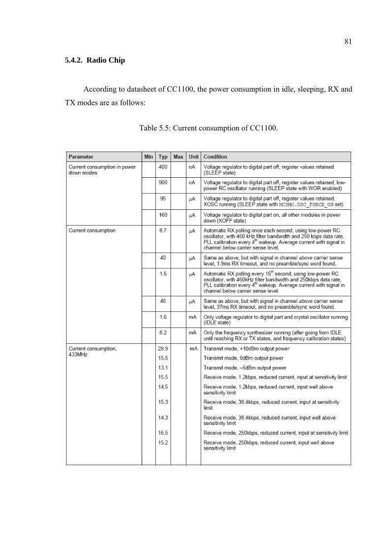
81
5.4.2. Radio Chip
According to datasheet of CC1100, the power consumption in idle, sleeping, RX and
TX modes are as follows:
Table 5.5: Current consumption of CC1100.
82
6. CONCLUSION
In the scope of this project, we developed a flexible but powerful framework to send,
receive and process data wirelessly between nodes. Also, we developed various different
device drivers including hardware abstraction library of some.
We used MSP430 and CC1100. Results show that, these two is a good combination
for low power and low cost applications. MSP430F169, with its 12-bit ADC and DAC,
cooperating with DMA module and hardware multiplier is a powerful chip for censoring or
simple signal processing applications. CC1100 is a powerful RF Transceiver operating in
various frequencies in sub-1 GHz and provides up to 500 kbps data rate is a good solution
for wireless support.
Another observation is, this hardware has much more technology (in the means of
hardware and software) than required for an Entryphone application or Walkie-Talkie.
IMA’s ADPCM implementation is a good solution for this kind of limited
applications, providing good sound quality. Since MSP430 has limited computational
power, we can’t use any more complicated codec. But, for further development, a better
codec can be implemented and used. The codec is very important because it directly affects
data rate, and data rate is directly affecting the radio sensitivity limit and operating range.
XXTEA is a really good algorithm providing a very good security as well as
requiring low computational power and memory. Any other crypto algorithm cannot be
used for this project because of the limited resources.
83
6.1. Further Development
This project can be further developed in some ways:
• A RTS/CTS mechanism can be implemented, and a solution is also should be
implemented for hidden node problem, for the transmission protocol.
• The range of this system is very limited for an advanced Entryphone system
that can be applied to a tall building for example. So, a repeating system
should be implemented between nodes. But, it is really hard and complicated
because of the real-time data transfer.
• A better codec or encryption system can be used with running CPU in higher
frequencies (like 8 MHz) in trade of power consumption.
• An external codec chip or encryption chip can be used to reduce the load on
CPU and enhance the remaining mechanism.
• A MCU or chip that has integrated encryption peripheral can be used, but
MSP430 does not have that kind of variant.
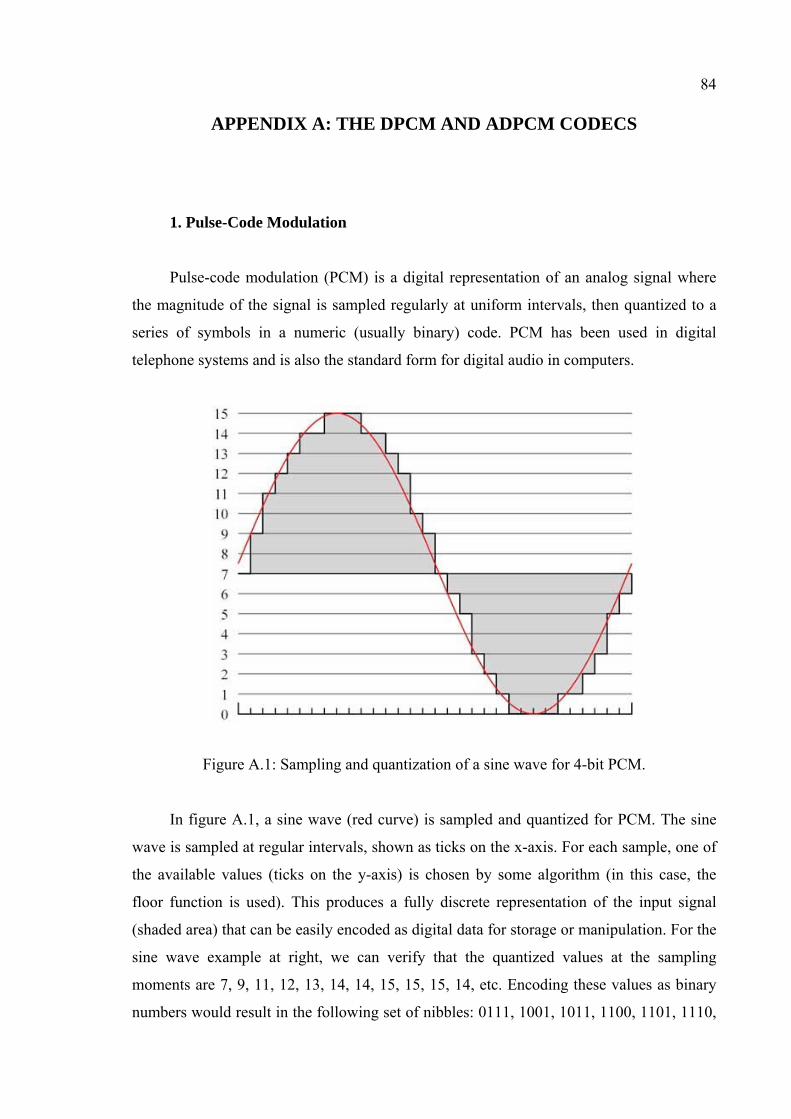
84
APPENDIX A: THE DPCM AND ADPCM CODECS
1. Pulse-Code Modulation
Pulse-code modulation (PCM) is a digital representation of an analog signal where
the magnitude of the signal is sampled regularly at uniform intervals, then quantized to a
series of symbols in a numeric (usually binary) code. PCM has been used in digital
telephone systems and is also the standard form for digital audio in computers.
Figure A.1: Sampling and quantization of a sine wave for 4-bit PCM.
In figure A.1, a sine wave (red curve) is sampled and quantized for PCM. The sine
wave is sampled at regular intervals, shown as ticks on the x-axis. For each sample, one of
the available values (ticks on the y-axis) is chosen by some algorithm (in this case, the
floor function is used). This produces a fully discrete representation of the input signal
(shaded area) that can be easily encoded as digital data for storage or manipulation. For the
sine wave example at right, we can verify that the quantized values at the sampling
moments are 7, 9, 11, 12, 13, 14, 14, 15, 15, 15, 14, etc. Encoding these values as binary
numbers would result in the following set of nibbles: 0111, 1001, 1011, 1100, 1101, 1110,

85
1110, 1111, 1111, 1111, 1110, etc. These digital values could then be further processed or
analyzed by a purpose-specific digital signal processor or general purpose CPU. Several
Pulse Code Modulation streams could also be multiplexed into a larger aggregate data
stream, generally for transmission of multiple streams over a single physical link. This
technique is called time-division multiplexing, or TDM, and is widely used, notably in the
modern public telephone system.
There are many ways to implement a real device that performs this task. In real
systems, such a device is commonly implemented on a single integrated circuit that lacks
only the clock necessary for sampling, and is generally referred to as an ADC (Analog-to-
Digital converter). These devices will produce on their output a binary representation of
the input whenever they are triggered by a clock signal, which would then be read by a
processor of some sort.
In conventional PCM, the analog signal may be processed (e.g. by amplitude
compression) before being digitized. Once the signal is digitized, the PCM signal is usually
subjected to further processing (e.g. digital data compression).
Some forms of PCM combine signal processing with coding. Older versions of these
systems applied the processing in the analog domain as part of the A/D process, newer
implementations do so in the digital domain. These simple techniques have been largely
rendered obsolete by modern transform-based audio compression techniques.
2. Differential Pulse Code Modulation (DPCM)
Differential (or Delta) pulse-code modulation (DPCM) encodes the PCM values as
differences between the current and the previous value. For audio this type of encoding
reduces the number of bits required per sample by about 25% compared to PCM. Predict
the next sample based on the last few decoded samples.
One of the simplest and fastest methods for lossy audio compression is differential
pulse code modulation or DPCM. This algorithm utilizes the fact that the ear is sensitive
for small differences when the volume is low, while, when the volume is loud, we can not
perceive subtle details to the same extent. Since there is no subband filtering, the noise
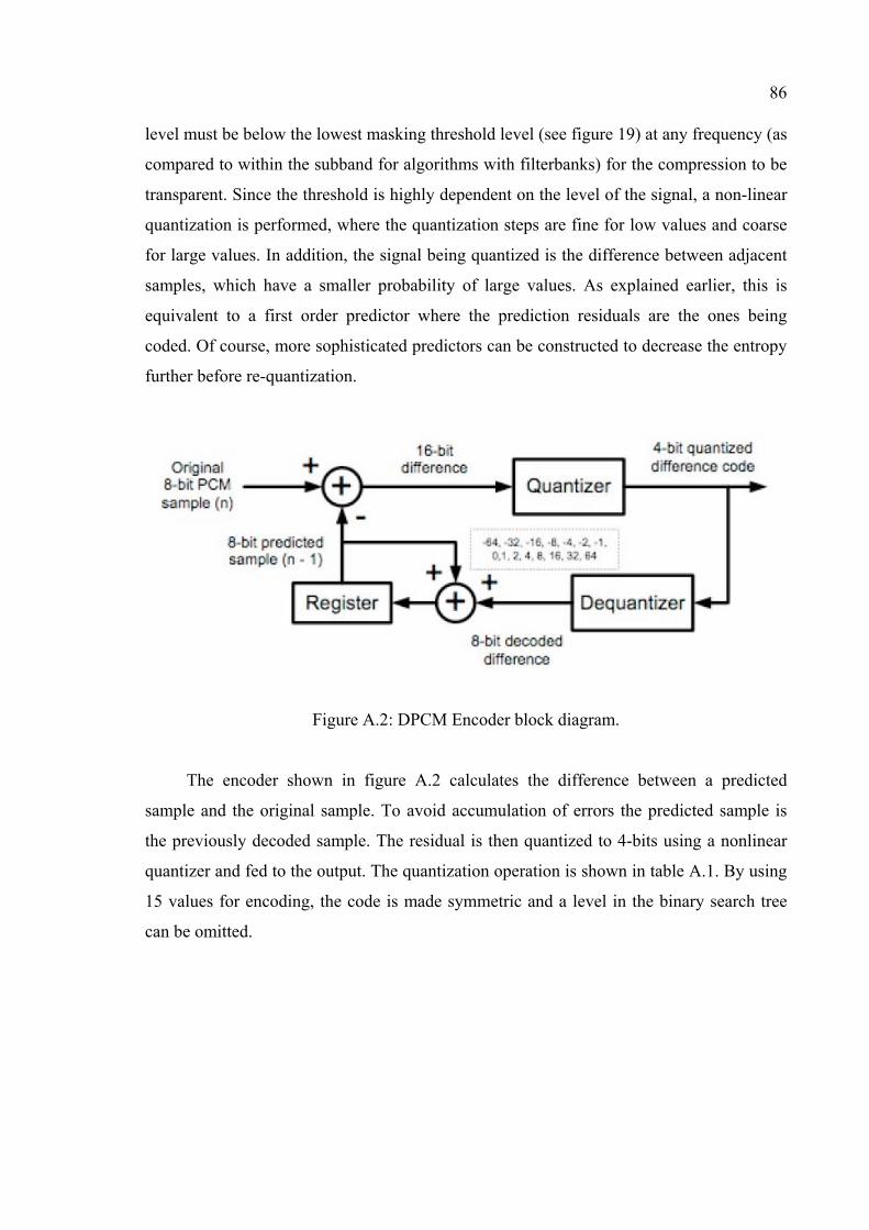
86
level must be below the lowest masking threshold level (see figure 19) at any frequency (as
compared to within the subband for algorithms with filterbanks) for the compression to be
transparent. Since the threshold is highly dependent on the level of the signal, a non-linear
quantization is performed, where the quantization steps are fine for low values and coarse
for large values. In addition, the signal being quantized is the difference between adjacent
samples, which have a smaller probability of large values. As explained earlier, this is
equivalent to a first order predictor where the prediction residuals are the ones being
coded. Of course, more sophisticated predictors can be constructed to decrease the entropy
further before re-quantization.
Figure A.2: DPCM Encoder block diagram.
The encoder shown in figure A.2 calculates the difference between a predicted
sample and the original sample. To avoid accumulation of errors the predicted sample is
the previously decoded sample. The residual is then quantized to 4-bits using a nonlinear
quantizer and fed to the output. The quantization operation is shown in table A.1. By using
15 values for encoding, the code is made symmetric and a level in the binary search tree
can be omitted.

87
Table A.1: DPCM non-linear quantization code.
The decoding is very simple. The 4-bit word is requantized to 8-bits using a
quantizer with an opposite transfer function of the one given in table 5. Then the necessary
prediction is done (when the input is the difference between two adjacent samples, the next
output value is obviously the sum of the current output value and the next difference).
Figure A.3: DPCM decoder block diagram.
One other thing should also be noted when regarding prediction in combination with
requantization: the predicted values are small when the differences between samples are
small and big when the differences are big. Small differences of course mean low
frequencies, while big differences mean high frequencies. Thus a noise-shaping is
performed, where the noise is moved up in frequency. When one look at the equal loudness
curves or the masking curve in figure 19, it becomes evident that moving the noise to high
frequencies is a good thing. Also, the total noise effect will decrease since less energy
exists in the high treble range. Actually, prediction is equivalent to delta-modulation, a
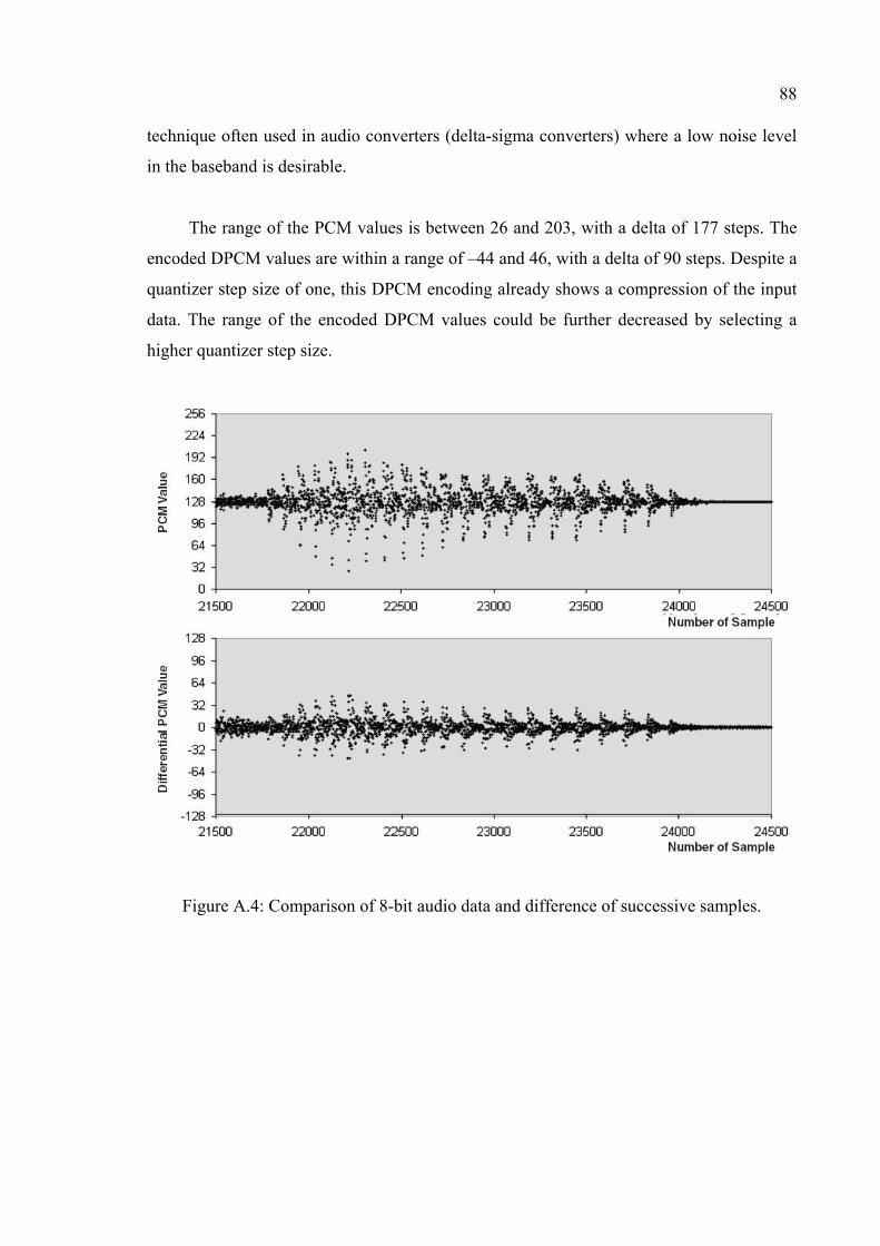
88
technique often used in audio converters (delta-sigma converters) where a low noise level
in the baseband is desirable.
The range of the PCM values is between 26 and 203, with a delta of 177 steps. The
encoded DPCM values are within a range of –44 and 46, with a delta of 90 steps. Despite a
quantizer step size of one, this DPCM encoding already shows a compression of the input
data. The range of the encoded DPCM values could be further decreased by selecting a
higher quantizer step size.
Figure A.4: Comparison of 8-bit audio data and difference of successive samples.
89
3. Adaptive Differential Pulse Code Modulation (ADPCM)
Adaptive PCM or ADPCM is a variant of DPCM that varies the quantization step
size. Amplitude variations of speech input signals are seen between different speakers or
between voiced and unvoiced segments of the speech input signal. The adaptation of the
quantizer step size takes place every sample and ensures equal encoding efficiency for both
low and high input signal amplitudes.
ADPCM is a further development of DPCM where the quantizer and/or the predictor
is adaptive. This means they are adjusted according to the nature of the input signal. If the
input signal is small, the quantizer steps are small, if the input signal is large, the quantizer
steps are large. This gives less error than the fixed nonlinear quantizer and the low,
constant bitrate can be maintained.
ADPCM is very widespread in telephone communications and speech coding and
many different algorithms exist. The Interactive Multimedia Association (IMA)
recommended a standard for ADPCM-codec in multimedia applications, known as IMA or
DVI ADPCM, in the early 1990s. This algorithm is now used in most cross-platform
ADPCM-based audio applications. In this report, a general explanation of the concepts
behind ADPCM will be given, while any specifics will be in accordance with the IMA-
standard.
The ADPCM-structure is very similar to the normal DPCM-structure, the difference
being that the quantizer, the predictor or both are adaptive.
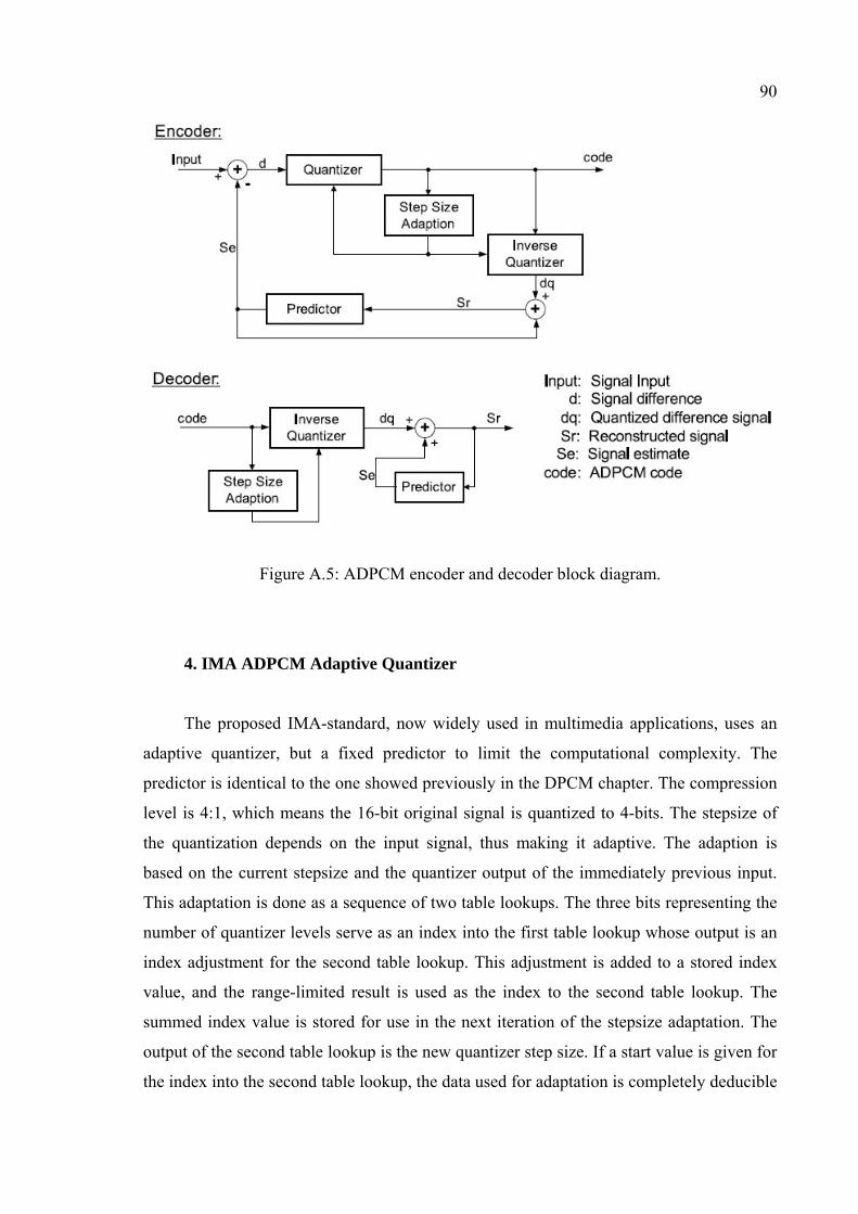
90
Figure A.5: ADPCM encoder and decoder block diagram.
4. IMA ADPCM Adaptive Quantizer
The proposed IMA-standard, now widely used in multimedia applications, uses an
adaptive quantizer, but a fixed predictor to limit the computational complexity. The
predictor is identical to the one showed previously in the DPCM chapter. The compression
level is 4:1, which means the 16-bit original signal is quantized to 4-bits. The stepsize of
the quantization depends on the input signal, thus making it adaptive. The adaption is
based on the current stepsize and the quantizer output of the immediately previous input.
This adaptation is done as a sequence of two table lookups. The three bits representing the
number of quantizer levels serve as an index into the first table lookup whose output is an
index adjustment for the second table lookup. This adjustment is added to a stored index
value, and the range-limited result is used as the index to the second table lookup. The
summed index value is stored for use in the next iteration of the stepsize adaptation. The
output of the second table lookup is the new quantizer step size. If a start value is given for
the index into the second table lookup, the data used for adaptation is completely deducible
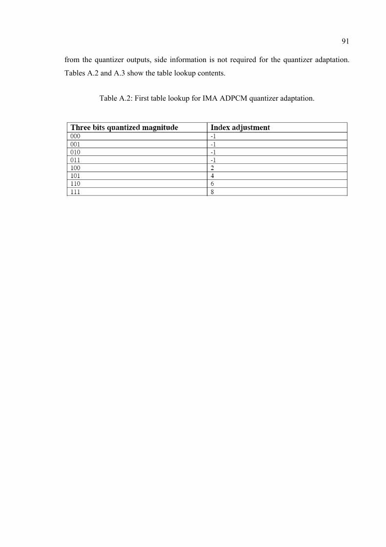
91
from the quantizer outputs, side information is not required for the quantizer adaptation.
Tables A.2 and A.3 show the table lookup contents.
Table A.2: First table lookup for IMA ADPCM quantizer adaptation.
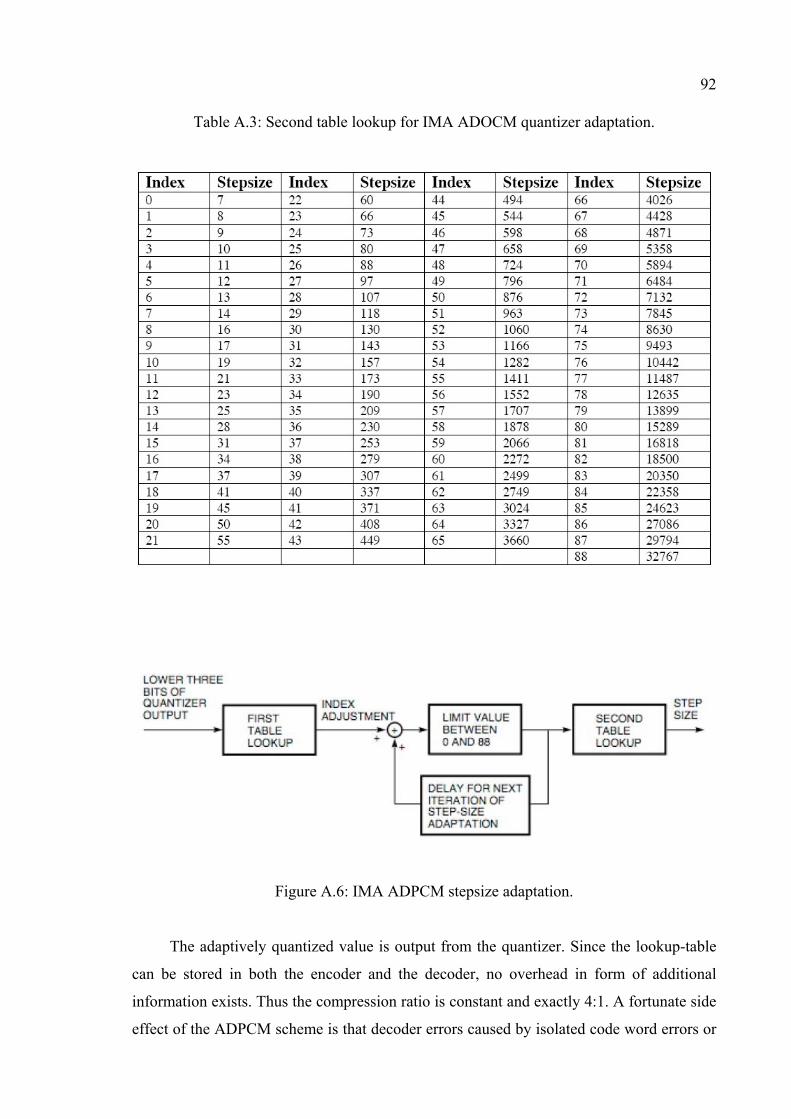
92
Table A.3: Second table lookup for IMA ADOCM quantizer adaptation.
Figure A.6: IMA ADPCM stepsize adaptation.
The adaptively quantized value is output from the quantizer. Since the lookup-table
can be stored in both the encoder and the decoder, no overhead in form of additional
information exists. Thus the compression ratio is constant and exactly 4:1. A fortunate side
effect of the ADPCM scheme is that decoder errors caused by isolated code word errors or
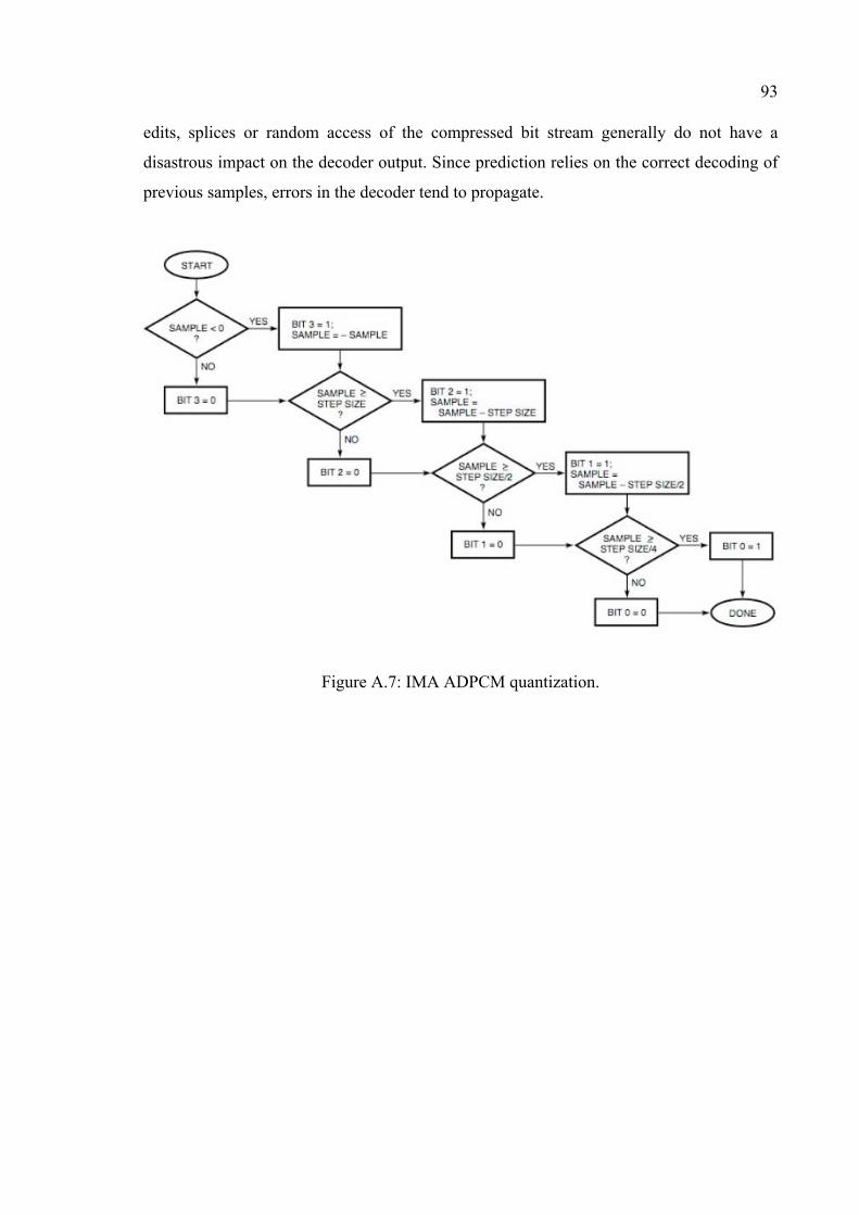
93
edits, splices or random access of the compressed bit stream generally do not have a
disastrous impact on the decoder output. Since prediction relies on the correct decoding of
previous samples, errors in the decoder tend to propagate.
Figure A.7: IMA ADPCM quantization.
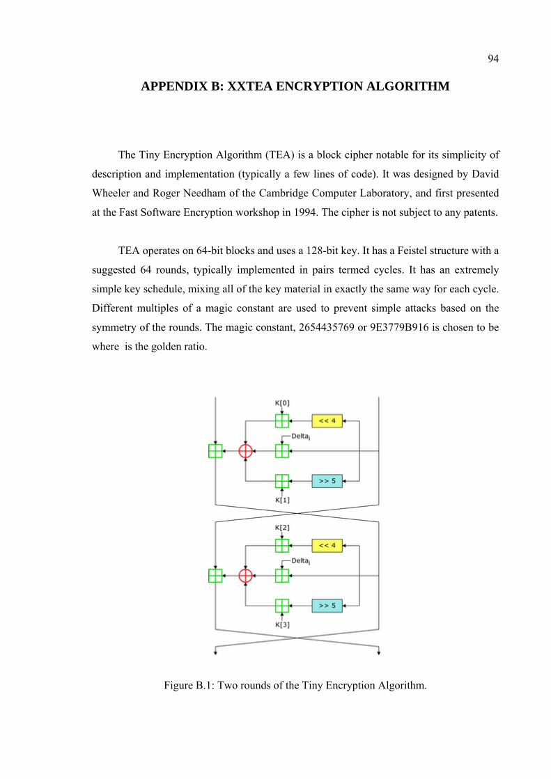
94
APPENDIX B: XXTEA ENCRYPTION ALGORITHM
The Tiny Encryption Algorithm (TEA) is a block cipher notable for its simplicity of
description and implementation (typically a few lines of code). It was designed by David
Wheeler and Roger Needham of the Cambridge Computer Laboratory, and first presented
at the Fast Software Encryption workshop in 1994. The cipher is not subject to any patents.
TEA operates on 64-bit blocks and uses a 128-bit key. It has a Feistel structure with a
suggested 64 rounds, typically implemented in pairs termed cycles. It has an extremely
simple key schedule, mixing all of the key material in exactly the same way for each cycle.
Different multiples of a magic constant are used to prevent simple attacks based on the
symmetry of the rounds. The magic constant, 2654435769 or 9E3779B916 is chosen to be
where is the golden ratio.
Figure B.1: Two rounds of the Tiny Encryption Algorithm.

95
TEA has a few weaknesses. Most notably, it suffers from equivalent keys — each
key is equivalent to three others, which means that the effective key size is only 126 bits.
As a result, TEA is especially bad as a cryptographic hash function. This weakness led to a
method for hacking Microsoft's Xbox game console, where the cipher was used as a hash
function. TEA is also susceptible to a related-key attack which requires 223 chosen
plaintexts under a related-key pair, with 232 time complexity. Because of these
weaknesses, a number of revisions of TEA have been designed.
The unusually small size of the TEA algorithm would make it a viable option in
situations where there are extreme constraints e.g. legacy hardware systems (perhaps
embedded) where the amount of available RAM is minimal.
The first published version of TEA was supplemented by a second version which
incorporated extensions to TEA to make it more secure. 'Block TEA' (sometimes referred
to as XTEA), operates on arbitrary-size blocks in place of the 64-bit blocks of the original.
A third version (XXTEA), published in 1998, described Corrections to xtea to
enhance the security of the Block TEA algorithm.
XTEA (eXtended TEA) is a block cipher designed to correct weaknesses in TEA.
Like TEA, XTEA is a 64-bit block Feistel network with a 128-bit key and a suggested 64
rounds. Several differences from TEA are apparent, including a somewhat more complex
key-schedule and a rearrangement of the shifts, XORs, and additions.
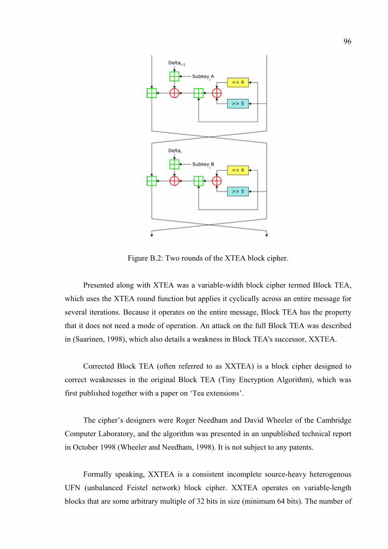
96
Figure B.2: Two rounds of the XTEA block cipher.
Presented along with XTEA was a variable-width block cipher termed Block TEA,
which uses the XTEA round function but applies it cyclically across an entire message for
several iterations. Because it operates on the entire message, Block TEA has the property
that it does not need a mode of operation. An attack on the full Block TEA was described
in (Saarinen, 1998), which also details a weakness in Block TEA's successor, XXTEA.
Corrected Block TEA (often referred to as XXTEA) is a block cipher designed to
correct weaknesses in the original Block TEA (Tiny Encryption Algorithm), which was
first published together with a paper on ‘Tea extensions’.
The cipher’s designers were Roger Needham and David Wheeler of the Cambridge
Computer Laboratory, and the algorithm was presented in an unpublished technical report
in October 1998 (Wheeler and Needham, 1998). It is not subject to any patents.
Formally speaking, XXTEA is a consistent incomplete source-heavy heterogenous
UFN (unbalanced Feistel network) block cipher. XXTEA operates on variable-length
blocks that are some arbitrary multiple of 32 bits in size (minimum 64 bits). The number of
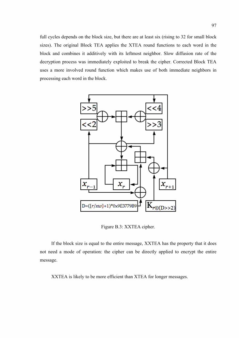
97
full cycles depends on the block size, but there are at least six (rising to 32 for small block
sizes). The original Block TEA applies the XTEA round functions to each word in the
block and combines it additively with its leftmost neighbor. Slow diffusion rate of the
decryption process was immediately exploited to break the cipher. Corrected Block TEA
uses a more involved round function which makes use of both immediate neighbors in
processing each word in the block.
Figure B.3: XXTEA cipher.
If the block size is equal to the entire message, XXTEA has the property that it does
not need a mode of operation: the cipher can be directly applied to encrypt the entire
message.
XXTEA is likely to be more efficient than XTEA for longer messages.
98
Needham & Wheeler make the following comments on the use of Block TEA:
• For ease of use and general security the large block version is to be preferred
when applicable for the following reasons.
• A single bit change will change about one half of the bits of the entire block,
leaving no place where the changes start.
• There is no choice of mode involved.
• Even if the correct usage of always changing the data sent (possibly by a
message number) is employed, only identical messages give the same result
and the information leakage is minimal.
• The message number should always be checked as this redundancy is the
check against a random message being accepted.
• Cut and join attacks do not appear to be possible.
• If it is not acceptable to have very long messages, they can be broken into
chunks say of 60 words and chained analogously to the methods used for
DES.

99
REFERENCES
1. Ying-Wen Bai and Shi-Chang Chen, “Design and Implementation of Home Intercom
and Security Control Systems for Buildings”, Consumer Electronics, 2007. ISCE 2007.
IEEE International Symposium on 20-23 June 2007.
2. Ammer, M.J., Sheets, M., Karalar, T., Kuulasa, M. and Rabaey, J., “A low-energy chip-
set for wireless intercom”, Design Automation Conference, 2003
3. Olavarrieta, L.D. and Nava, A.A., “Wireless communications: a bird's eye view of an
emerging technology”, Communications and Information Technology, IEEE ISCIT,
2004.
4. Taylor, R.M., “Space communications”, IEEE Volume 29, Issue 2, Feb. 1992.
5. Bernard Sklar, “Digital Communications: Fundamentals and Applications”, Second
Edition, Prentice Hall, 2001.
6. Ming Yang, “Low Bit Rate Speech Coding”, Potentials, IEEE Volume 23, Issue 4,
Oct-Nov 2004.
7. Gersho, A., “Advances in speech and audio compression”, Proceedings of the IEEE
Volume 82, Issue 6, June 1994.
8. Khalifa, O.O., Islam, M.D.R., Khan, S., Shebani, M.S., “Communications
cryptography”, RF and Microwave Conference, 2004.
9. William Stallings, “Network Security Essentials: Applications and Standards”, Prentica
Hall, 1999.
10. Roger M. Needham and David J. Wheeler, “TEA Extensions”, unpublished, 1997.

100
11. David J. Wheeler and Roger M. Needham, “Correction to XTEA”, unpublished, 1998.
12. “MSP430x1xx Family User’s Guide”, Texas Instruments Inc., 2003.
13. Chris Nagy, “Embedded Systems Design using the TI MSP430 Series”, Elsevier, 2003.
14. “CC1100 - Single Chip Low Cost Low Power RF Transceiver”, Texas Instruments
Inc., 2006.
15. “Hitachi - HD44780U LCD Datasheet”, Hitachi, 2000.
16. John G. Proakis and Masoud Salahi, “Communications Systems Engineering, Second
Edition”, Prentice Hall, 2002.
17. Sherif, M.H., Bowker, D.O., Bertocci, G., Orford, B.A., Mariano, G.A., “Overview and
performance of CCITT/ANSI embedded ADPCM algorithms”, IEEE Transactions on
Volume 41, Feb. 1993.
18. Ivar Loekken, “Wireless Loudspeaker System With Real-Time Audio Compression”,
NTNU Master Thesis, unpublished, 2004.
19. Hager, C.T.R., Midkiff, S.F., Park, J.-M., Martin, T.L., “Performance and Energy
Efficiency of Block Ciphers in Personal Digital Assistants”, Pervasive Computing and
Communications, 2005.


![[MSP430] ADC10](https://static.fdocuments.net/doc/165x107/55cf97c5550346d033938430/msp430-adc10-5654b9a37ede3.jpg)

![Vortrag zur Seminarphase der PG „Solar Doorplate“ MSP430 ... · MSP430 – Wichtigste Grundlagen von David Tondorf. 2 ... MSP430 microcontroller basics. Oxford: Newnes [4] MSP430](https://static.fdocuments.net/doc/165x107/5b6f6a9b7f8b9af12d8c481e/vortrag-zur-seminarphase-der-pg-solar-doorplate-msp430-msp430-.jpg)