
A Tamper-Resistant Watt-Hour Energy Meter Based on the AD7751
24
REV. 0 a AN-574 APPLICATION NOTE INTRODUCTION This application note describes a low cost, high accu- racy IEC1036 Class 1 watt-hour meter based on the AD7751. The meter described is intended for use in single phase, two-wire distribution systems. The AD7751 is a low-cost, single chip solution for electri- cal energy measurement. The most distinctive feature of the AD7751 is that it continuously monitors the phase and neutral (return) currents. A FAULT condition occurs if the two currents differ by more than 12.5%. Power cal- culation will be based on the larger of the two currents. The meter calculates power correctly even if one of the two wires does not carry any current. AD7751 provides an effective way to combat any attempt to return the current through earth, a very simple yet effective way of meter tampering. The AD7751 comprises of two ADCs, reference circuit and all the signal processing neces- sary for the calculation of real (active) power. The AD7751 also includes direct drive capability for electro- mechanical counters (i.e., the energy register) and has a high-frequency pulse output for calibration and communications purposes. This application note should be used in conjunction with the AD7751 data sheet. The data sheet provides detailed information on the functionality of the AD7751 and will be referenced several times in this application note. DESIGN GOALS The international Standard IEC1036 (1996-09)—Alternat- ing current watt-hour meters for active energy (Classes 1 and 2), was used as the primary specification for this design. For readers more familiar with the ANSI C12.16 specification, see the section at the end of this applica- tion which compares the IEC1036 and ANSI C12.16 standards. This section explains the key IEC1036 specifi- cations in terms of their ANSI equivalents. The design greatly exceeds this basic specification for many of the accuracy requirements, e.g., accuracy at unity power factor and at low (PF = ±0.5) power factor. In addition, the dynamic range performance of the meter has been extended to 500. The IEC1036 standard speci- fies accuracy over a range of 5% I B to I MAX —see Table I. Typical values for I MAX are 400% to 600% of I B . Table I outlines the accuracy requirements for a static watt- hour meter. The current range (dynamic range) for accuracy is specified in terms of I B (basic current). Table I. Accuracy Requirements Percentage Error Limits 3 Current Value 1 PF 2 Class 1 Class 2 0.05 I B ≤ I < 0.1 I B 1 ±1.5% ±2.5% 0.1 I B ≤ I ≤ I MAX 1 ±1.0% ±2.0% 0.1 I B ≤ I ≤ 0.2 I B 0.5 Lag ±1.5% ±2.5% 0.8 Lead ±1.5% — 0.2 I B ≤ I ≤ I MAX 0.5 Lag ±1.0% ±2.0% 0.8 Lead ±1.0% — NOTES 1 The current ranges for specified accuracy shown in Table I are expressed in terms of the basic current (I B ). The basic current is defined in IEC1036 (1996-09) section 3.5.1.2 as the value of current in accordance with which the relevant performance of a transformer operated meter is fixed. I MAX is the maximum current at which accuracy is maintained. 2 Power Factor (PF) in Table I relates the phase relationship between the fundamental (45 Hz to 65 Hz) voltage and current waveforms. PF in this case can be simply defined as PF = cos(θ), where θ is the phase angle between pure sinusoidal current and voltage. 3 Class index is defined in IEC1036 (1996-09) section 3.5.5 as the limits of the permissible percentage error. The percentage error is defined as: Percen energy registered by meter true energy true energy tage Error = − × 100% The schematic in Figure 1 shows the implementation of a tamper-resistant, low-cost watt-hour meter using the AD7751. A current transformer (CT) is used to detect the current in the neutral wire, and the current flowing in the phase is monitored by a current shunt. These two cur- rent sensors provide the current to voltage conversion needed by the AD7751 and a simple divider network attenuates the line voltage. The energy register (kWh) is a simple electromechanical counter that uses a two- phase stepper motor. The AD7751 provides direct drive capability for this type of counter. The AD7751 also pro- vides a high-frequency output at the CF pin for the meter constant (3200 imp/kWh). Thus a high-frequency output is available at the LED and optoisolator output. This high-frequency output is used to speed up the calibra- tion process and provides a means of quickly verifying A Tamper-Resistant Watt-Hour Energy Meter Based on the AD7751 with a Current Transformer and a Low Resistant Shunt by William Koon One Technology Way • P.O. Box 9106 • Norwood, MA 02062-9106 • Tel: 781/329-4700 • Fax: 781/326-8703 • www.analog.com © Analog Devices, Inc., 2001
-
Upload
truongkiet -
Category
Documents
-
view
222 -
download
0
Transcript of A Tamper-Resistant Watt-Hour Energy Meter Based on the AD7751
REV. 0
a AN-574APPLICATION NOTE
INTRODUCTION
This application note describes a low cost, high accu-racy IEC1036 Class 1 watt-hour meter based on theAD7751. The meter described is intended for use insingle phase, two-wire distribution systems.
The AD7751 is a low-cost, single chip solution for electri-cal energy measurement. The most distinctive feature ofthe AD7751 is that it continuously monitors the phaseand neutral (return) currents. A FAULT condition occursif the two currents differ by more than 12.5%. Power cal-culation will be based on the larger of the two currents.The meter calculates power correctly even if one of thetwo wires does not carry any current. AD7751 providesan effective way to combat any attempt to return thecurrent through earth, a very simple yet effective way ofmeter tampering. The AD7751 comprises of two ADCs,reference circuit and all the signal processing neces-sary for the calculation of real (active) power. TheAD7751 also includes direct drive capability for electro-mechanical counters (i.e., the energy register) and hasa high-frequency pulse output for calibration andcommunications purposes.
This application note should be used in conjunction withthe AD7751 data sheet. The data sheet provides detailedinformation on the functionality of the AD7751 and willbe referenced several times in this application note.
DESIGN GOALS
The international Standard IEC1036 (1996-09)—Alternat-ing current watt-hour meters for active energy (Classes1 and 2), was used as the primary specification for thisdesign. For readers more familiar with the ANSI C12.16specification, see the section at the end of this applica-tion which compares the IEC1036 and ANSI C12.16standards. This section explains the key IEC1036 specifi-cations in terms of their ANSI equivalents.
The design greatly exceeds this basic specification formany of the accuracy requirements, e.g., accuracy atunity power factor and at low (PF = ±0.5) power factor. Inaddition, the dynamic range performance of the meterhas been extended to 500. The IEC1036 standard speci-fies accuracy over a range of 5% IB to IMAX—see Table I.
Typical values for IMAX are 400% to 600% of IB. Table Ioutlines the accuracy requirements for a static watt-hour meter. The current range (dynamic range) foraccuracy is specified in terms of IB (basic current).
Table I. Accuracy Requirements
Percentage Error Limits3
Current Value1 PF2 Class 1 Class 2
0.05 IB ≤ I < 0.1 IB 1 ±1.5% ±2.5%0.1 IB ≤ I ≤ IMAX 1 ±1.0% ±2.0%0.1 IB ≤ I ≤ 0.2 IB 0.5 Lag ±1.5% ±2.5%
0.8 Lead ±1.5% —0.2 IB ≤ I ≤ IMAX 0.5 Lag ±1.0% ±2.0%
0.8 Lead ±1.0% —
NOTES1The current ranges for specified accuracy shown in Table I are expressedin terms of the basic current (IB). The basic current is defined in IEC1036(1996-09) section 3.5.1.2 as the value of current in accordance with whichthe relevant performance of a transformer operated meter is fixed. I MAX
is the maximum current at which accuracy is maintained.2Power Factor (PF) in Table I relates the phase relationship between thefundamental (45 Hz to 65 Hz) voltage and current waveforms. PF in thiscase can be simply defined as PF = cos(θ), where θ is the phase anglebetween pure sinusoidal current and voltage.
3Class index is defined in IEC1036 (1996-09) section 3.5.5 as the limits ofthe permissible percentage error. The percentage error is defined as:
Percen
energy registered by meter true energytrue energy
tage Error = − × 100%
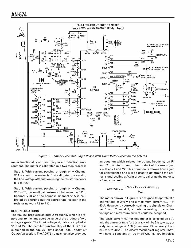
The schematic in Figure 1 shows the implementation ofa tamper-resistant, low-cost watt-hour meter using theAD7751. A current transformer (CT) is used to detect thecurrent in the neutral wire, and the current flowing in thephase is monitored by a current shunt. These two cur-rent sensors provide the current to voltage conversionneeded by the AD7751 and a simple divider networkattenuates the line voltage. The energy register (kWh) isa simple electromechanical counter that uses a two-phase stepper motor. The AD7751 provides direct drivecapability for this type of counter. The AD7751 also pro-vides a high-frequency output at the CF pin for the meterconstant (3200 imp/kWh). Thus a high-frequency outputis available at the LED and optoisolator output. Thishigh-frequency output is used to speed up the calibra-tion process and provides a means of quickly verifying
A Tamper-Resistant Watt-Hour Energy Meter Based on the AD7751with a Current Transformer and a Low Resistant Shunt
by William Koon
One Technology Way • P.O. Box 9106 • Norwood, MA 02062-9106 • Tel: 781/329-4700 • Fax: 781/326-8703 • www.analog.com
© Analog Devices, Inc., 2001
–2–
AN-574
REV. 0
meter functionality and accuracy in a production envi-ronment. The meter is calibrated in a two-step process:
Step 1. With current passing through only ChannelV1A’s shunt, the meter is first calibrated by varyingthe line voltage attenuation using the resistor networkR14 to R23.
Step 2. With current passing through only ChannelV1B’s CT, the small gain mismatch between the CT’ inChannel V1B and the shunt in Channel V1A is cali-brated by shorting out the appropriate resistor in theresistor network R8 to R13.
DESIGN EQUATIONS
The AD7751 produces an output frequency which is pro-portional to the time average value of the product of twovoltage signals. The input voltage signals are applied atV1 and V2. The detailed functionality of the AD7751 isexplained in the AD7751 data sheet—see Theory OfOperation section. The AD7751 data sheet also provides
–
+
–
+
K1Z3 J22
R5A100
C2033nF
K3
R62.7 R7
56 R882
R9160
R132.7k
J16 J17
J20
J21
J19J18
R121.3k
R11680
R10330
Z4K2
+
R1
1k
R2
1k
R3
1.05k
C133nF
C333nF
C233nF
C433nF
R4A1k
C533nF
R4B1k
J23
R5B100
C2133nF
P4
P5
P6
P7
P8
SOLDER JUMPERSCALIBRATION
NETWORK3%
LOAD
J518k
J10560
J1300k
J2150k
J375k
J439k
J69.1k
J75.1k
J82.2k
J91.2k
R18
R19
R20
R21
R22
R23
R14
R15
R16
R17
C610F
C7100nF
CALIBRATIONNETWORK30%
Z1K5
K6
R24
330k
R25
330k
C1710nF
X2MOV1S20K275
C18470nF R26
470
D21N4744A
D21N4004
C19470F35V Z2
8 1
2,3,6,7
POWER SUPPLYU2
7805VDD+5V
P11P9
P10
P21
VDD
R2710k
+
+
+
C12220F6.3V
C11100nF
C13100nF
C1410F6.3V
R33
10
P3 P1P2
VDD
NE
UT
RA
L
PH
AS
E
240V
R32
20
R31
20
R29
820
C16
C15
K7
K8
TO IMPULSE COUNTER/STEPPER MOTOR
100IMP/kWhr
R30
820
D4
CALIBRATION LEDHP HLMP-D150
FAULT LEDHP HLMP-D150
U3
PS2501-1
1
2 3
4
3200IMP/kWhr
K9
K10
3.579545MHz
C1022pF
C922pF
Y1
VDD
R2810k
J15
J11
J12
J13
J14
C8100nF 0R 0R
JUMPERSUSE 0RESISTORS
G0 = 1G1 = 1S0 = 1S1 = 0SCF = 0
P23
P17
P18
P19
P20
P22
P23
P16
P15
P14
P13
P12
AVDD AC/DC DVDD
F1
F2
CF
DEVP
FAULT
CLKOUT
CLKIN
G0
G1
S0
S1
SCF
V1A
V1B
V1N
V2N
V2P
REFIN/OUT
RESET AGND DGND
U1AD7751
FAULT TOLERANT ENERGY METERIMAX = 40A, Ib = 5A, CLASS 1 (5% Ib – IMAX)
K4
D1
Figure 1. Tamper-Resistant Single Phase Watt-Hour Meter Based on the AD7751
an equation which relates the output frequency on F1and F2 (counter drive) to the product of the rms signallevels at V1 and V2. This equation is shown here againfor convenience and will be used to determine the cor-rect signal scaling at V2 in order to calibrate the meter toa fixed constant.
Frequency
V V Gain F
VREF
= × × × × −5 74 1 2 1 42
.(1)
The meter shown in Figure 1 is designed to operate at aline voltage of 240 V and a maximum current (IMAX) of40 A. However by correctly scaling the signals on Chan-nel 1 and Channel 2, a meter operating of any linevoltage and maximum current could be designed.
The basic current (IB) for this meter is selected as 5 A,and the current range for accuracy will be 5% IB to IMAX ora dynamic range of 160 (maintains 1% accuracy from250 mA to 40 A). The electromechanical register (kWh)will have a constant of 100 imp/kWh, i.e., 100 impulses
–3–
AN-574
REV. 0
from the AD7751 will be required in order to register1 kWh. IEC1036 section 4.2.11 specifies that electromag-netic registers have their lowest values numbered in tendivision, each division being subdivided into ten parts.Hence a display with a five plus one digits is used, i.e.,10,000s, 1,000s, 100s, 10s, 1s, 1/10s. The meter constant(for calibration and test) is selected as 3200 imp/kWh.The on-chip reference circuit of the AD7751 has a tem-perature coefficient of typically 30 ppm/°C. However, onA grade parts this specification is not guaranteed andmay be as high as 80 ppm/°C. At 80 ppm/°C the AD7751error at –20°C/+60°C would be approximately +0.65%,assuming a calibration at 25°C.
Shunt Selection
The shunt size (500 µΩ) is selected to maximize the useof the dynamic range on Channel V1A (current ChannelA). However, there are some important considerationswhen selecting a shunt for an energy metering applica-tion. First, minimize the power dissipation in the shunt.The maximum rated current for this design is 40 A,therefore the maximum power dissipated in the shunt is(40 A)2 × 500 µΩ = 800 mW. IEC1036 calls for a maximumpower disposition of 2 W (including power supply). Sec-ondly, the higher power dissipation may make it difficultto manage the thermal issues. Although the shunt ismanufactured from Manganin material which is an alloywith a low temperature coefficient of resistance, hightemperatures may cause significant error at heavyloads. A third consideration is the ability of the meter toresist attempts to tamper by shorting the circuit exter-nally. With a very low value of shunt resistance, theeffects of externally shorting the shunt are very muchminimized. Therefore, the shunt should always bemade as small as possible, but this must be offsetagainst the signal range on V1A (30 mV rms with a gainof 16). If the shunt is made too small, it will not be pos-sible to meet the IEC1036 accuracy requirements at lightloads. A shunt value of 500 µΩ was considered a goodcompromise for this design.
Current Transformer (CT) Selection
The CTs and their burden resistors should be selected tomatch the shunt selected for V1B input. However thereare some important considerations when selecting theCTs and the burden resistors for energy metering appli-cation. First, one need to select CTs that have goodlinearity in both their gain and phase characteristicsover the range of current specified in the accuracyrequirement. For IEC1036, the range is between 5% IB toIMAX. CT manufacturers often recommend the burdenresistance to be as small as possible to preserve linear-ity over large current range. A burden resistance of lessthan 15 Ω is recommended. Second, CT introduces aphase shift between primary and secondary current. Thephase shift can contribute to a significant error at lowpower factor. Note that at power factor of 0.5, a phaseshift as small as 0.1° translates to 0.3% error in the
power reading. In this design, the phase of the CT chan-nel (V1B) is shifted to match the phase shift introducedby the CT to eliminate any phase mismatch between thecurrent and voltage channel. This is achieved by mov-ing the corner frequency of the antialiasing filter in thecurrent channel input—see Corrected Phase Matchingbetween Channels and Antialias Filters in this applica-tion note. In this design, a 5000 turn CT was chosen. Thenominal value of the burden resistor can be found by thefollowing calculation:
Burden Resistor = CT Turn Ratio × Shunt Resistance
Design Calculations
Design parameters:Line Voltage = 240 V (Nominal)IMAX = 40 A (IB = 5 A)Counter = 100 imp/kWhMeter Constant = 3200 imp/kWh
Shunt Resistance = 500 µΩCT Turn Ratio = 1:5000Nominal Burden Resistor = 500 µΩ × 5000 = 2.5 Ω
100 imp/hour = 100 ÷ 3600 sec = 0.027777 HzMeter will be calibrated at IB (5 A).Power dissipation at IB = 240 V × 5 A = 1.2 kWFrequency on F1 (and F2) at IB = 1.2 × 0.027777 Hz = 0.03333333 Hz
Voltage across the shunt at IB (V1A) = 5A × 500 µΩ =2.5 mV.
To select the F1-4 frequency for Equation 1, see theAD7751 data sheet—Selecting a Frequency for an EnergyMeter Application. From Tables V and VI in the AD7751data sheet it can be seen that the best choice of fre-quency for a meter with IMAX = 40 A is 3.4 Hz (F2). Thisfrequency selection is made by the logic inputs S0 andS1—see Table II in the AD7751 data sheet. The CFfrequency selection (meter constant) is selected byusing the logic input SCF. The two available options are64 × F1(6400 imp/kWh) or 32 × F1(3200 imp/kWh). Forthis design, 3200 imp/kWh is selected by setting SCFlogic low. With a meter constant of 3200 imp/kWh and amaximum current of 40 A, the maximum frequency fromCF is 8.53 Hz. Many calibration benches used to verifymeter accuracy still use optical techniques. This limitsthe maximum frequency which can be reliably read toabout 10 Hz. The only remaining unknown from Equa-tion 1 is V2 or the signal level on Channel 2 (thevoltage channel).
From Equation 1 on the previous page:
0 03333333
5 74 2 5 2 16 3 452
.. . .
.Hz
mV V Hz= × × × ×2
where:
V2 = 266.8 mV rms
–4–
AN-574
REV. 0
Therefore, in order to calibrate the meter, the line voltageneeds to be attenuated down to 266.8 mV.
CALIBRATING THE METER: VOLTAGE CHANNEL
CALIBRATION
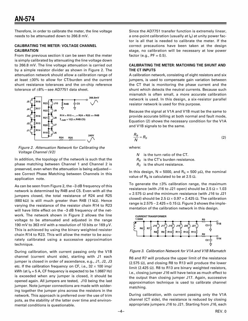
From the previous section it can be seen that the meteris simply calibrated by attenuating the line voltage downto 266.8 mV. The line voltage attenuation is carried outby a simple resistor divider as shown in Figure 2. Theattenuation network should allow a calibration range ofat least ±30% to allow for CT/burden and the currentshunt resistance tolerances and the on-chip referencetolerance of ±8%—see AD7751 data sheet.
R4BJ5
J10
J1
J2
J3
J4
J6
J7
J8
J9
R18
R19
R20
R21
R22
R23
R14
R15
R16
R17
C5
266.8mV
240VR25R24
R14 + R15 +....+ R24 + R25 >> R4B
f–3dB = 1/(2..R4B.C5)
Figure 2. Attenuation Network for Calibrating theVoltage Channel (V2)
In addition, the topology of the network is such that thephase matching between Channel 1 and Channel 2 ispreserved, even when the attenuation is being adjusted—see Correct Phase Matching between Channels in thisapplication note.
As can be seen from Figure 2, the –3 dB frequency of thisnetwork is determined by R4B and C5. Even with all thejumpers closed, the total resistance of R24 and R25(660 kΩ) is still much greater than R4B (1 kΩ). Hencevarying the resistance of the resistor chain R14 to R23will have little effect on the –3 dB frequency of the net-work. The network shown in Figure 2 allows the linevoltage to be attenuated and adjusted in the range190 mV to 363 mV with a resolution of 10 bits or 169 µV.This is achieved by using the binary weighted resisterchain R14 to R23. This will allow the meter to be accu-rately calibrated using a successive approximationtechnique.
During calibration, with current passing only the V1Bchannel (current shunt side), starting with J1 eachjumper is closed in order of ascendance, e.g., J1, J2, J3etc. If the calibration frequency on CF, i.e., 32 × 100 imp/kWh (at IB = 5 A, CF frequency is expected to be 1.0667 Hz)is exceeded when any jumper is closed, it should beopened again. All jumpers are tested, J10 being the lastjumper. Note jumper connections are made with solder-ing together the jumper pins across the resistors in thenetwork. This approach is preferred over the use of trimpots, as the stability of the latter over time and environ-mental conditions is questionable.
Since the AD7751 transfer function is extremely linear,a one-point calibration (usually at IB) at unity power fac-tor is all that is needed to calibrate the meter. If thecorrect precautions have been taken at the designstage, no calibration will be necessary at low powerfactor (e.g., PF = 0.5).
CALIBRATING THE METER: MATCHING THE SHUNT AND
THE CT INPUTS
A calibration network, consisting of eight resistors and sixjumpers, is used to compensate gain variation betweenthe CT that is monitoring the phase current and theshunt which detects the neutral currents. Because suchmismatch is often small, a more accurate calibrationnetwork is used. In this design, a six-resistor parallelresistor network is used for this purpose.
Because the signal at V1A and V1B must be the same toprovide accurate billing at both normal and fault mode,Equation (2) shows the necessary condition for the V1Aand V1B signals to be the same.
RN
RBS= (2)
where:
N is the turn ratio of the CT.RB is the CT’s burden resistance.RS is the shunt resistance.
In this design, N = 5000, and RS = 500 µΩ, the nominalvalue of RB is calculated to be at 2.5 Ω.
To generate the ±3% calibration range, the maximumresistance (with J16 to J21 open) should be 2.5 Ω × 1.03= 2.575 Ω and the minimum resistance (with J16 to J21closed) should be 2.5 Ω × 0.97 = 2.425 Ω. The calibrationrange is 2.575 – 2.425 = 0.15 Ω. Figure 3 shows the imple-mentation of the calibration network in this design.
R6 R7
R8 R9 R13
J16 J17 J21
R12
J20
R11
J19
R10
J18
R2
R3
C3
C2
V1B
V1N
CURRENT TRANSFORMER1:5000
Figure 3. Calibration Network for V1A and V1B Mismatch
R6 and R7 will produce the upper limit of the resistance(2.575 Ω), and closing R8 to R13 will produce the lowerlimit (2.425 Ω). R8 to R13 are binary weighted resistors,i.e., closing jumper J16 will have twice as much effect tothe output than closing jumper J17. Again, successiveapproximation technique is used to calibrate channelmatching.
During calibration, with current passing only the V1Achannel (CT side), the resistance is reduced by closingappropriate jumpers J16 to J21. Starting from J16, each
–5–
AN-574
REV. 0
jumper is closed. By putting extra resistor in parallel, thetotal burden resistance is reduced and thus the outputsignal is attenuated. If the calibration frequency fallsbelow the expected value after a jumper is closed, thejumper should be opened again.
Note that similar to the voltage calibration network, thephase angle is preserved to be the same as that of Chan-nel V1A by selecting the appropriate resistance valuesused in the network.
CORRECT PHASE MATCHING BETWEEN CHANNELS
The AD7751 is internally phase-matched over the fre-quency range 40 Hz to 1 kHz. Correct phase matching isimportant in an energy metering application becauseany phase mismatch between channels will translateinto significant errors at low power factor. This is easilyillustrated with the following example. Figure 4 showsthe voltage and current waveforms for an inductiveload. In the example shown, the current lags the voltageby 60° (PF = 0.5). Assuming pure sinusoidal conditions,the power is easily calculated as V rms × I rms × cos (60°).
60
VOLTAGE
CURRENT
INSTANTANEOUSPOWER SIGNAL
INSTANTANEOUS REALPOWER SIGNAL
CURRENT
PF = 1
PF = 0.5
VOLTAGE
INSTANTANEOUSPOWER SIGNAL
INSTANTANEOUS REALPOWER SIGNAL
V.I2
V.I.2
COS(60)
Figure 4 . Voltage and Current Waveform(Inductive Load)
If, however, a phase error (e) is introduced externallyto the AD7751, e.g., in the antialias filters, the error iscalculated as:
[cos (δ°) – cos (δ° + φe)]/cos (δ°) × 100% (3)
See Note 3 in Table I. Where δ is the phase angle betweenvoltage and current and φe is the external phase error.
With a phase error of 0.2°, for example, the error at PF = 0.5(60°) is calculated as 0.6%. As this example demon-strates, even a very small phase error will produce alarge measurement error at low power factor.
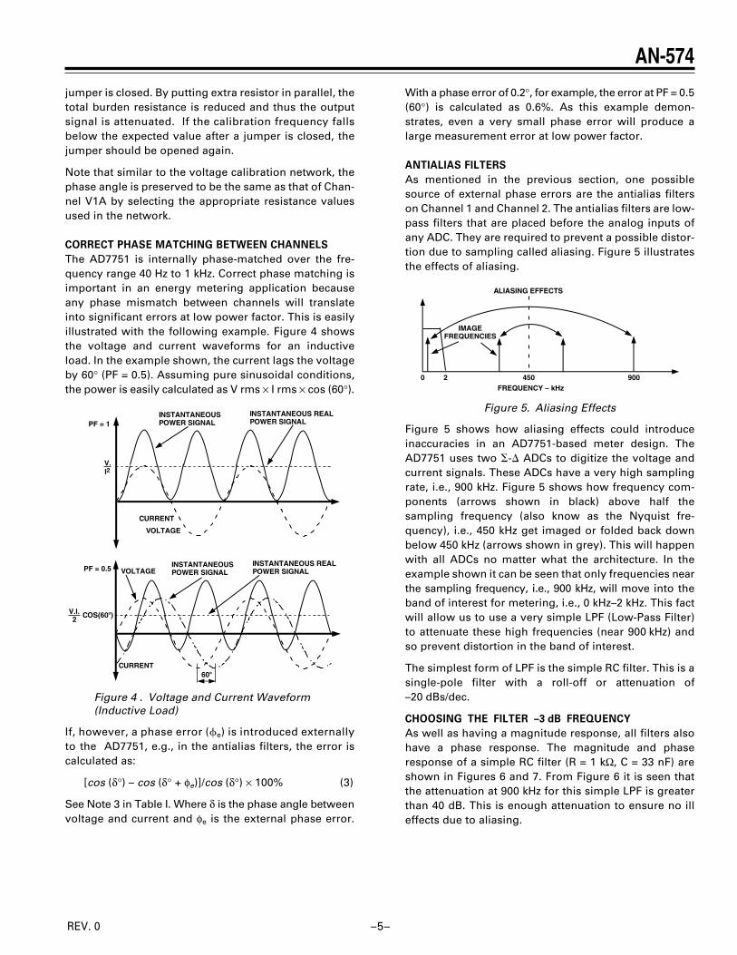
ANTIALIAS FILTERS
As mentioned in the previous section, one possiblesource of external phase errors are the antialias filterson Channel 1 and Channel 2. The antialias filters are low-pass filters that are placed before the analog inputs ofany ADC. They are required to prevent a possible distor-tion due to sampling called aliasing. Figure 5 illustratesthe effects of aliasing.
FREQUENCY – kHz
ALIASING EFFECTS
0 450 900 2
IMAGEFREQUENCIES
Figure 5. Aliasing Effects
Figure 5 shows how aliasing effects could introduceinaccuracies in an AD7751-based meter design. TheAD7751 uses two - ADCs to digitize the voltage andcurrent signals. These ADCs have a very high samplingrate, i.e., 900 kHz. Figure 5 shows how frequency com-ponents (arrows shown in black) above half thesampling frequency (also know as the Nyquist fre-quency), i.e., 450 kHz get imaged or folded back downbelow 450 kHz (arrows shown in grey). This will happenwith all ADCs no matter what the architecture. In theexample shown it can be seen that only frequencies nearthe sampling frequency, i.e., 900 kHz, will move into theband of interest for metering, i.e., 0 kHz–2 kHz. This factwill allow us to use a very simple LPF (Low-Pass Filter)to attenuate these high frequencies (near 900 kHz) andso prevent distortion in the band of interest.
The simplest form of LPF is the simple RC filter. This is asingle-pole filter with a roll-off or attenuation of–20 dBs/dec.
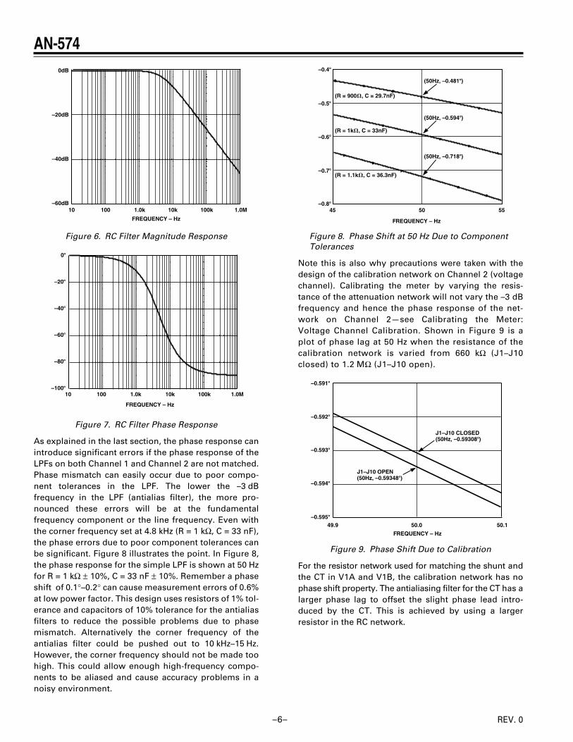
CHOOSING THE FILTER –3 dB FREQUENCY
As well as having a magnitude response, all filters alsohave a phase response. The magnitude and phaseresponse of a simple RC filter (R = 1 kΩ, C = 33 nF) areshown in Figures 6 and 7. From Figure 6 it is seen thatthe attenuation at 900 kHz for this simple LPF is greaterthan 40 dB. This is enough attenuation to ensure no illeffects due to aliasing.
–6–
AN-574
REV. 0
10 100 1.0k 10k 100k 1.0M FREQUENCY – Hz
0dB
–20dB
–40dB
–60dB
Figure 6. RC Filter Magnitude Response
10 100 1.0k 10k 100k 1.0M
FREQUENCY – Hz
0
–20
–40
–60
–80
–100
Figure 7. RC Filter Phase Response
As explained in the last section, the phase response canintroduce significant errors if the phase response of theLPFs on both Channel 1 and Channel 2 are not matched.Phase mismatch can easily occur due to poor compo-nent tolerances in the LPF. The lower the –3 dBfrequency in the LPF (antialias filter), the more pro-nounced these errors will be at the fundamentalfrequency component or the line frequency. Even withthe corner frequency set at 4.8 kHz (R = 1 kΩ, C = 33 nF),the phase errors due to poor component tolerances canbe significant. Figure 8 illustrates the point. In Figure 8,the phase response for the simple LPF is shown at 50 Hzfor R = 1 kΩ ± 10%, C = 33 nF ± 10%. Remember a phaseshift of 0.1°–0.2° can cause measurement errors of 0.6%at low power factor. This design uses resistors of 1% tol-erance and capacitors of 10% tolerance for the antialiasfilters to reduce the possible problems due to phasemismatch. Alternatively the corner frequency of theantialias filter could be pushed out to 10 kHz–15 Hz.However, the corner frequency should not be made toohigh. This could allow enough high-frequency compo-nents to be aliased and cause accuracy problems in anoisy environment.
45 50 55
FREQUENCY – Hz
–0.4
(50Hz, –0.594)
(50Hz, –0.718)
(50Hz, –0.481)
–0.5
–0.6
–0.7
–0.8
(R = 1k, C = 33nF)
(R = 900, C = 29.7nF)
(R = 1.1k, C = 36.3nF)
Figure 8. Phase Shift at 50 Hz Due to ComponentTolerances
Note this is also why precautions were taken with thedesign of the calibration network on Channel 2 (voltagechannel). Calibrating the meter by varying the resis-tance of the attenuation network will not vary the –3 dBfrequency and hence the phase response of the net-work on Channel 2—see Calibrating the Meter:Voltage Channel Calibration. Shown in Figure 9 is aplot of phase lag at 50 Hz when the resistance of thecalibration network is varied from 660 kΩ (J1–J10closed) to 1.2 MΩ (J1–J10 open).
49.9 50.0 50.1
FREQUENCY – Hz
–0.591
–0.592
–0.593
–0.594
–0.595
J1–J10 CLOSED(50Hz, –0.59308)
J1–J10 OPEN(50Hz, –0.59348)
Figure 9. Phase Shift Due to Calibration
For the resistor network used for matching the shunt andthe CT in V1A and V1B, the calibration network has nophase shift property. The antialiasing filter for the CT has alarger phase lag to offset the slight phase lead intro-duced by the CT. This is achieved by using a largerresistor in the RC network.
–7–
AN-574
REV. 0
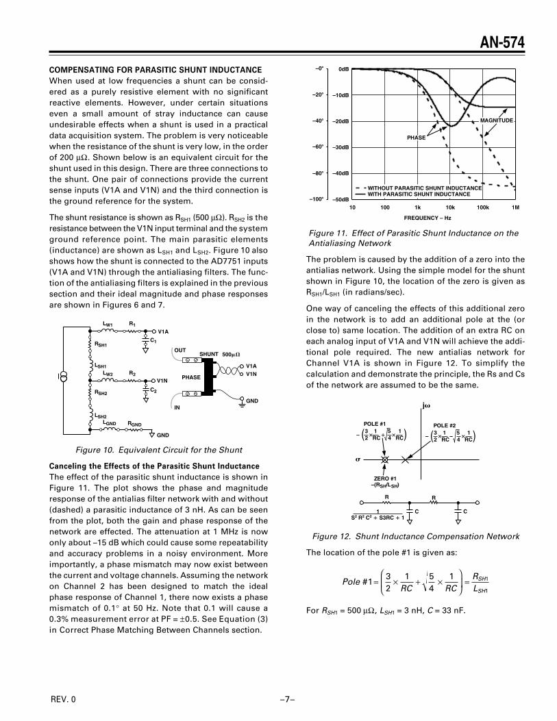
COMPENSATING FOR PARASITIC SHUNT INDUCTANCE
When used at low frequencies a shunt can be consid-ered as a purely resistive element with no significantreactive elements. However, under certain situationseven a small amount of stray inductance can causeundesirable effects when a shunt is used in a practicaldata acquisition system. The problem is very noticeablewhen the resistance of the shunt is very low, in the orderof 200 µΩ. Shown below is an equivalent circuit for theshunt used in this design. There are three connections tothe shunt. One pair of connections provide the currentsense inputs (V1A and V1N) and the third connection isthe ground reference for the system.
The shunt resistance is shown as RSH1 (500 µΩ). RSH2 is theresistance between the V1N input terminal and the systemground reference point. The main parasitic elements(inductance) are shown as LSH1 and LSH2. Figure 10 alsoshows how the shunt is connected to the AD7751 inputs(V1A and V1N) through the antialiasing filters. The func-tion of the antialiasing filters is explained in the previoussection and their ideal magnitude and phase responsesare shown in Figures 6 and 7.
LW1
LGND
LW2
R1
RGND
R2
RSH1
RSH2
LSH1
LSH2
C1
C2
V1A
V1N
GND
OUT
IN
PHASE
SHUNT 500
V1AV1N
GND
Figure 10. Equivalent Circuit for the Shunt
Canceling the Effects of the Parasitic Shunt Inductance
The effect of the parasitic shunt inductance is shown inFigure 11. The plot shows the phase and magnituderesponse of the antialias filter network with and without(dashed) a parasitic inductance of 3 nH. As can be seenfrom the plot, both the gain and phase response of thenetwork are effected. The attenuation at 1 MHz is nowonly about –15 dB which could cause some repeatabilityand accuracy problems in a noisy environment. Moreimportantly, a phase mismatch may now exist betweenthe current and voltage channels. Assuming the networkon Channel 2 has been designed to match the idealphase response of Channel 1, there now exists a phasemismatch of 0.1° at 50 Hz. Note that 0.1 will cause a0.3% measurement error at PF = ±0.5. See Equation (3)in Correct Phase Matching Between Channels section.
WITHOUT PARASITIC SHUNT INDUCTANCEWITH PARASITIC SHUNT INDUCTANCE
10 100 1k 10k 100k 1M
–100
–80
–60
–40
–20
–0
–50dB
–40dB
–30dB
–20dB
–10dB
0dB
FREQUENCY – Hz
MAGNITUDE
PHASE
Figure 11. Effect of Parasitic Shunt Inductance on the Antialiasing Network
The problem is caused by the addition of a zero into theantialias network. Using the simple model for the shuntshown in Figure 10, the location of the zero is given asRSH1/LSH1 (in radians/sec).
One way of canceling the effects of this additional zeroin the network is to add an additional pole at the (orclose to) same location. The addition of an extra RC oneach analog input of V1A and V1N will achieve the addi-tional pole required. The new antialias network forChannel V1A is shown in Figure 12. To simplify thecalculation and demonstrate the principle, the Rs and Csof the network are assumed to be the same.
ZERO #1–(RSH/LSH)
j
POLE #1 POLE #2 3 1 5 12 RC 4 RC
– – ( )
R R
C C
3 1 5 12 RC 4 RC– ( )
1S2 R2 C2 S3RC 1
Figure 12. Shunt Inductance Compensation Network
The location of the pole #1 is given as:
PoleRC RC
RL
SH
SH#1
32
1 54
1 1
1= × + ×
=
For RSH1 = 500 µΩ, LSH1 = 3 nH, C = 33 nF.
–8–
AN-574
REV. 0
R is calculated as approximately 476 Ω (Use 470 Ω).
The location of Pole #1 is 166,667 rads or 26.53 kHz.
This places the location of Pole # 2 at:
PoleRC RC
kHz# .232
1 54
13 920= × + ×
=
To ensure phase matching between Channel 1 andChannel 2, the pole at Channel 2 must also be positionedat this location. With C = 33 nF, the new value of resistancefor the antialias filters on Channel 2 is approximately1.23 kΩ (use 1.2 kΩ).
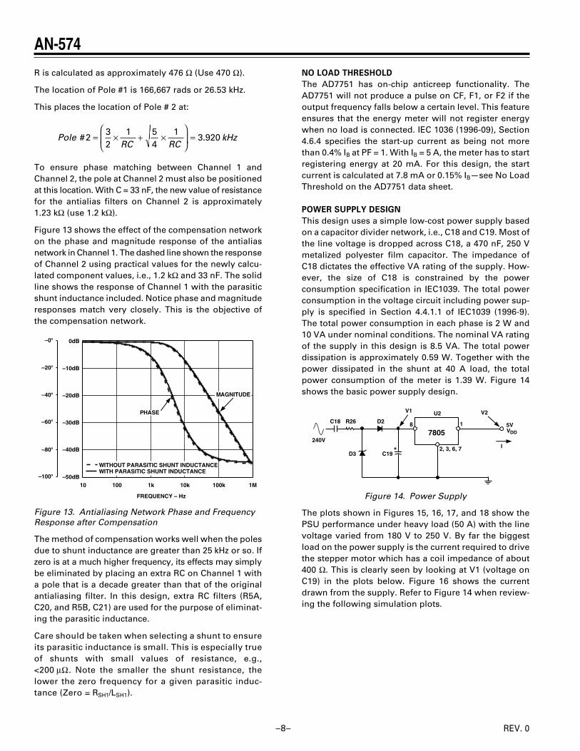
Figure 13 shows the effect of the compensation networkon the phase and magnitude response of the antialiasnetwork in Channel 1. The dashed line shown the responseof Channel 2 using practical values for the newly calcu-lated component values, i.e., 1.2 kΩ and 33 nF. The solidline shows the response of Channel 1 with the parasiticshunt inductance included. Notice phase and magnituderesponses match very closely. This is the objective ofthe compensation network.
WITHOUT PARASITIC SHUNT INDUCTANCEWITH PARASITIC SHUNT INDUCTANCE
10 100 1k 10k 100k 1M
–100
–80
–60
–40
–20
–0
–50dB
–40dB
–30dB
–20dB
–10dB
0dB
FREQUENCY – Hz
MAGNITUDE
PHASE
Figure 13. Antialiasing Network Phase and FrequencyResponse after Compensation
The method of compensation works well when the polesdue to shunt inductance are greater than 25 kHz or so. Ifzero is at a much higher frequency, its effects may simplybe eliminated by placing an extra RC on Channel 1 witha pole that is a decade greater than that of the originalantialiasing filter. In this design, extra RC filters (R5A,C20, and R5B, C21) are used for the purpose of eliminat-ing the parasitic inductance.
Care should be taken when selecting a shunt to ensureits parasitic inductance is small. This is especially trueof shunts with small values of resistance, e.g.,<200 µΩ. Note the smaller the shunt resistance, thelower the zero frequency for a given parasitic induc-tance (Zero = RSH1/LSH1).
NO LOAD THRESHOLD
The AD7751 has on-chip anticreep functionality. TheAD7751 will not produce a pulse on CF, F1, or F2 if theoutput frequency falls below a certain level. This featureensures that the energy meter will not register energywhen no load is connected. IEC 1036 (1996-09), Section4.6.4 specifies the start-up current as being not morethan 0.4% IB at PF = 1. With IB = 5 A, the meter has to startregistering energy at 20 mA. For this design, the startcurrent is calculated at 7.8 mA or 0.15% IB—see No LoadThreshold on the AD7751 data sheet.
POWER SUPPLY DESIGN
This design uses a simple low-cost power supply basedon a capacitor divider network, i.e., C18 and C19. Most ofthe line voltage is dropped across C18, a 470 nF, 250 Vmetalized polyester film capacitor. The impedance ofC18 dictates the effective VA rating of the supply. How-ever, the size of C18 is constrained by the powerconsumption specification in IEC1039. The total powerconsumption in the voltage circuit including power sup-ply is specified in Section 4.4.1.1 of IEC1039 (1996-9).The total power consumption in each phase is 2 W and10 VA under nominal conditions. The nominal VA ratingof the supply in this design is 8.5 VA. The total powerdissipation is approximately 0.59 W. Together with thepower dissipated in the shunt at 40 A load, the totalpower consumption of the meter is 1.39 W. Figure 14shows the basic power supply design.
5VVDD7805
R26U2
D3
D2C18
C19
18
2, 3, 6, 7+
V1 V2
I240V
Figure 14. Power Supply
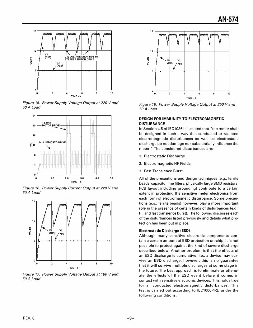
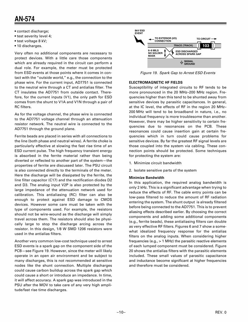
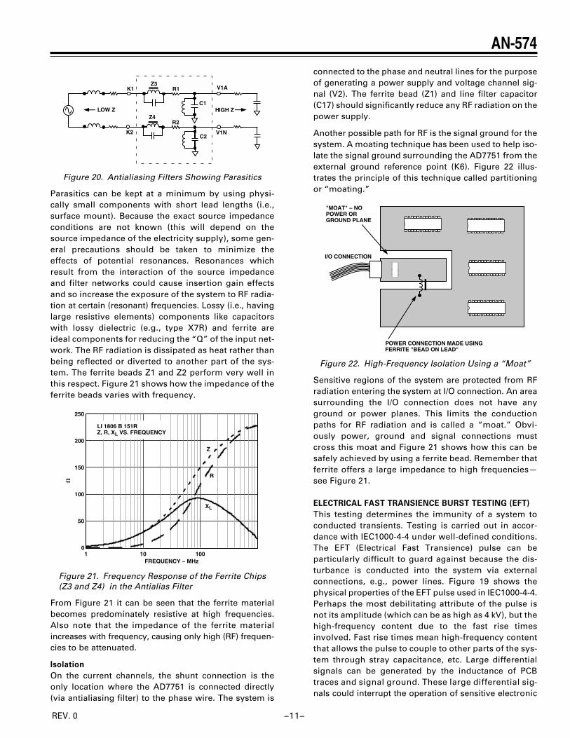
The plots shown in Figures 15, 16, 17, and 18 show thePSU performance under heavy load (50 A) with the linevoltage varied from 180 V to 250 V. By far the biggestload on the power supply is the current required to drivethe stepper motor which has a coil impedance of about400 Ω. This is clearly seen by looking at V1 (voltage onC19) in the plots below. Figure 16 shows the currentdrawn from the supply. Refer to Figure 14 when review-ing the following simulation plots.
–9–
AN-574
REV. 0
15
10
5
00 2 4 6 8 10
TIME – s
V1(C19)
V2(VDD)
C19 VOLTAGE DROP DUE TOSTEPPER MOTOR DRIVE
VOLT
S
Figure 15. Power Supply Voltage Output at 220 V and50 A Load
24
20
16
12
8
4
00 1.0 2.0 3.0 4.0 5.0
12.5mAMOTOR DRIVE
4mA LED/OPTO DRIVE
TIME – s
mA
Figure 16. Power Supply Current Output at 220 V and50 A Load
0 2 4 6 8 10
TIME – s
15
10
5
0
V2VDD
V1(C19)VO
LTS
Figure 17. Power Supply Voltage Output at 180 V and50 A Load
0 2 4 6 8 10
TIME – s
15
10
5
0
V2VDD
V1(C19)VO
LTS
Figure 18. Power Supply Voltage Output at 250 V and50 A Load
DESIGN FOR IMMUNITY TO ELECTROMAGNETIC
DISTURBANCE
In Section 4.5 of IEC1036 it is stated that “the meter shallbe designed in such a way that conducted or radiatedelectromagnetic disturbances as well as electrostaticdischarge do not damage nor substantially influence themeter.” The considered disturbances are:-
1. Electrostatic Discharge
2. Electromagnetic HF Fields
3. Fast Transience Burst
All of the precautions and design techniques (e.g., ferritebeads, capacitor line filters, physically large SMD resistors,PCB layout including grounding) contribute to a certainextent in protecting the sensitive meter electronics fromeach form of electromagnetic disturbance. Some precau-tions (e.g., ferrite beads) however, play a more importantrole in the presence of certain kinds of disturbances (e.g.,RF and fast transience burst). The following discusses eachof the disturbances listed previously and details what pro-tection has been put in place.
Electrostatic Discharge (ESD)
Although many sensitive electronic components con-tain a certain amount of ESD protection on-chip, it is notpossible to protect against the kind of severe dischargedescribed below. Another problem is that the effects ofan ESD discharge is cumulative, i.e., a device may sur-vive an ESD discharge; however, this is no guaranteethat it will survive multiple discharges at some stage inthe future. The best approach is to eliminate or attenu-ate the effects of the ESD event before it comes incontact with sensitive electronic devices. This holds truefor all conducted electromagnetic disturbances. Thistest is carried out according to IEC1000-4-2, under thefollowing conditions:
–10–
AN-574
REV. 0
• contact discharge;• test severity level 4;• test voltage 8 kV;• 10 discharges.
Very often no additional components are necessary toprotect devices. With a little care those componentswhich are already required in the circuit can perform adual role. For example, the meter must be protectedfrom ESD events at those points where it comes in con-tact with the “outside world,” e.g., the connection to thephase wire. For the current input, AD7751 is connectedto the neutral wire through a CT and antialias filter. TheCT insulates the AD7751 from outside contact. There-fore, for the current inputs (V1), the only path for ESDcomes from the shunt to V1A and V1N through a pair ofRC filters.
As for the voltage channel, the phase wire is connectedto the AD7751 voltage channel through an attenuationresistor network. The neutral wire is connected to theAD7751 through the ground plane.
Ferrite beads are placed in series with all connections tothe line (both phase and neutral wires). A ferrite choke isparticularly effective at slowing the fast rise time of anESD current pulse. The high frequency transient energyis absorbed in the ferrite material rather than beingdiverted or reflected to another part of the system—theproperties of ferrite are discussed later. The PSU circuitis also connected directly to the terminals of the meter.Here the discharge will be dissipated by the ferrite, theline filter capacitor (C17) and the rectification diodes D2and D3. The analog input V2P is also protected by thelarge impedance of the attenuation network used forcalibration. This antialiasing (RC) filter can also beenough to protect against ESD damage to CMOSdevices. However some care must be taken with thetype of components used. For example, the resistorsshould not be wire-wound as the discharge will simplytravel across them. The resistors should also be physi-cally large to stop the discharge arcing across theresistor. In this design, 1/8 W SMD 1206 resistors wereused in the antialias filters.
Another very common low-cost technique used to arrestESD events is a spark gap on the component side of thePCB—see Figure 19. However, since the meter will likelyoperate in an open air environment and be subject tomany discharges, this is not recommended at sensitivenodes like the shunt connection. Multiple dischargescould cause carbon buildup across the spark gap whichcould cause a short or introduce an impedance. In time,it will affect accuracy. A spark gap was introduced in thePSU after the MOV to take care of any very high ampli-tude/fast rise time discharges.
SIGNALGROUND
TRACE (TRACK)
TO EXTERIOR (I/O)CONNECTION
TO CIRCUIT
8kV ESDEVENT
ESD DISCHARGEDACROSS SPARK GAP
1036–9 MILSNO SOLDERMASK
Figure 19. Spark Gap to Arrest ESD Events
ELECTROMAGNETIC HF FIELDS
Susceptibility of integrated circuits to RF tends to bemore pronounced in the 20 MHz–200 MHz region. Fre-quencies higher than this tend to be shunted away fromsensitive devices by parasitic capacitances. In general,at the IC level, the effects of RF in the region 20 MHz–200 MHz will tend to be broadband in nature, i.e., noindividual frequency is more troublesome than another.However, there may be higher sensitivity to certain fre-quencies due to resonances on the PCB. Theseresonances could cause insertion gain at certain fre-quencies which in turn could cause problems forsensitive devices. By far the greatest RF signal levels arethose coupled into the system via cabling. These con-nection points should be protected. Some techniquesfor protecting the system are:
1. Minimize circuit bandwidth
2. Isolate sensitive parts of the system
Minimize Bandwidth
In this application, the required analog bandwidth isonly 2 kHz. This is a significant advantage when trying toreduce the effects of RF. The cable entry points can below-pass filtered to reduce the amount of RF radiationentering the system. The shunt output is already filteredbefore being connected to the AD7751. This is to preventaliasing effects described earlier. By choosing the correctcomponents and adding some additional components(e.g., ferrite beads), these antialiasing filters can doubleas very effective RF filters. Figures 6 and 7 show a some-what idealized frequency response for the antialiasfilters on the analog inputs. When considering higherfrequencies (e.g., > 1 MHz) the parasitic reactive elementsof each lumped component must be considered. Figure20 shows the antialias filters with the parasitic elementsincluded. These small values of parasitic capacitanceand inductance become significant at higher frequenciesand therefore must be considered.
–11–
AN-574
REV. 0
LOW Z HIGH Z
K1
K2
Z3
Z4
R1
R2
C1
C2
V1A
V1N
Figure 20. Antialiasing Filters Showing Parasitics
Parasitics can be kept at a minimum by using physi-cally small components with short lead lengths (i.e.,surface mount). Because the exact source impedanceconditions are not known (this will depend on thesource impedance of the electricity supply), some gen-eral precautions should be taken to minimize theeffects of potential resonances. Resonances whichresult from the interaction of the source impedanceand filter networks could cause insertion gain effectsand so increase the exposure of the system to RF radia-tion at certain (resonant) frequencies. Lossy (i.e., havinglarge resistive elements) components like capacitorswith lossy dielectric (e.g., type X7R) and ferrite areideal components for reducing the “Q” of the input net-work. The RF radiation is dissipated as heat rather thanbeing reflected or diverted to another part of the sys-tem. The ferrite beads Z1 and Z2 perform very well inthis respect. Figure 21 shows how the impedance of theferrite beads varies with frequency.
250
200
150
100
50
01 10 100
FREQUENCY – MHz
LI 1806 B 151RZ, R, XL VS. FREQUENCY
Z
R
XL
Figure 21. Frequency Response of the Ferrite Chips(Z3 and Z4) in the Antialias Filter
From Figure 21 it can be seen that the ferrite materialbecomes predominately resistive at high frequencies.Also note that the impedance of the ferrite materialincreases with frequency, causing only high (RF) frequen-cies to be attenuated.
Isolation
On the current channels, the shunt connection is theonly location where the AD7751 is connected directly(via antialiasing filter) to the phase wire. The system is
connected to the phase and neutral lines for the purposeof generating a power supply and voltage channel sig-nal (V2). The ferrite bead (Z1) and line filter capacitor(C17) should significantly reduce any RF radiation on thepower supply.
Another possible path for RF is the signal ground for thesystem. A moating technique has been used to help iso-late the signal ground surrounding the AD7751 from theexternal ground reference point (K6). Figure 22 illus-trates the principle of this technique called partitioningor “moating.”
I/O CONNECTION
"MOAT" – NOPOWER ORGROUND PLANE
POWER CONNECTION MADE USINGFERRITE "BEAD ON LEAD"
Figure 22. High-Frequency Isolation Using a “Moat”
Sensitive regions of the system are protected from RFradiation entering the system at I/O connection. An areasurrounding the I/O connection does not have anyground or power planes. This limits the conductionpaths for RF radiation and is called a “moat.” Obvi-ously power, ground and signal connections mustcross this moat and Figure 21 shows how this can besafely achieved by using a ferrite bead. Remember thatferrite offers a large impedance to high frequencies—see Figure 21.
ELECTRICAL FAST TRANSIENCE BURST TESTING (EFT)
This testing determines the immunity of a system toconducted transients. Testing is carried out in accor-dance with IEC1000-4-4 under well-defined conditions.The EFT (Electrical Fast Transience) pulse can beparticularly difficult to guard against because the dis-turbance is conducted into the system via externalconnections, e.g., power lines. Figure 19 shows thephysical properties of the EFT pulse used in IEC1000-4-4.Perhaps the most debilitating attribute of the pulse isnot its amplitude (which can be as high as 4 kV), but thehigh-frequency content due to the fast rise timesinvolved. Fast rise times mean high-frequency contentthat allows the pulse to couple to other parts of the sys-tem through stray capacitance, etc. Large differentialsignals can be generated by the inductance of PCBtraces and signal ground. These large differential sig-nals could interrupt the operation of sensitive electronic
–12–
AN-574
REV. 0
components. Digital systems are generally most atrisk because of data corruption. Analog electronicsystems tend only to be affected for the duration ofthe disturbance.
10%
50%
90%
TIME
5ns
50ns
4kV
Figure 23. Single EFT Pulse Characteristics
Another possible issue with conducted EFT is that theeffects of the radiation will, like ESD, generally be cumu-lative for electronic components. The energy in an EFTpulse can be as high as 4 mJ and deliver 40 A into a 50 Ωload—see Figure 26. Therefore continuous exposure toEFT due to inductive load switching, etc., may haveimplications for the long-term reliability of components.The best approach is to protect those parts of the systemthat could be sensitive to EFT.
The protection techniques described in the last section(Electromagnetic HF Fields) also apply equally well inthe case of EFT. The electronics should be isolated asmuch as possible from the source of the disturbancethrough PCB layout (i.e., moating) and filtering signaland power connections. In addition, a 10 nF capacitor(C17) placed across the mains provides a low-impedanceshunt for differential EFT pulses. Stray inductance dueto leads and PCB traces will mean that the MOV will notbe very effective in attenuating the differential EFTpulse. The MOV is very effective in attenuating highenergy, relatively long duration disturbances, e.g.,due to lighting strikes, etc. The MOV is discussed inthe next section.
MOV Type S20K275
The MOV used in this design was of type S20K275 fromSiemens. An MOV is basically an voltage-dependantresistor whose resistance decreases with increasingvoltage. MOVs are typically connected in parallel withthe device or circuit that is being protected. During anovervoltage event they form a low-resistance shunt andthus prevent any further rise in the voltage across thecircuit being protected. The overvoltage is essentiallydropped across the source impedance of the overvolt-age source, e.g., the mains network source impedance.Figure 24 illustrates the principle of operation.
VS
VB, VMOV
1
2
LEAKAGECURRENT » 0
SURGE CURRENT
"LOAD LINE"OF THE OVERVOLTAGE
V/I CHARACTERISTICCURVE OF MOV
V
i* i*it
V
VB
VS
OVERVOLTAGE SOURCE
ZS
MOVELECTRONICCIRCUIT TO BEPROTECTED
* TAKEN FROM SIEMENS MATSUSHITA COMPONENTS SIOV METAL OXIDE VARISTOR CATALOG
Figure 24. Principle of MOV Overvoltage Protection
The plot in Figure 24 shows how the MOV voltage andcurrent can be estimated for a given overvoltage andsource impedance. A load line (open circuit voltage,short circuit current) is plotted on the same graph as theMOV characteristic curve. Where the curves intersect,the MOV clamping voltage and current can be read.Note, care must be taken when determining the short-circuit current. The frequency content of the overvoltagemust be taken into account as the source impedance(e.g., mains) may vary considerably with frequency. Atypical impedance of 50 Ω is used for mains sourceimpedance during fast transience (high-frequency)pulse testing. The next section discusses IEC1000-4-4and IEC1000-4-5 which are transience and overvoltageEMC compliance tests.
IEC1000-4-4 and the S20K275
While the graphical technique just described is useful,an even better approach is to use simulation to obtain abetter understanding of MOV operation. SiemensMatsushita Components provides SPICE models for alltheir MOVs and these are very useful in determiningdevice operation under the various IEC EMC compliancetests. For more information on S&M SPICE models andtheir applications see:
http://www.siemens.de/pr/index.htm
The purpose of IEC1000-4-4 is to determine the effectof repetitive, low-energy, high-voltage, fast-rise-timepulses on an electronic system. This test is intended tosimulate transient disturbances such as those originat-ing from switching transience (e.g., interruption ofinductive loads, relay contact bounce, etc.).
Figure 21 shows an equivalent circuit which is intendedto replicate the EFT test pulse as specified in IEC1000-4-4.The generator circuit is based on Figure 1 IEC1000-4-4(1995-01). The characteristics of operation are:
–13–
AN-574
REV. 0
• Maximum Energy of 4mJ/pulse at 2 kV into 50 Ω
• Source Impedance of 50 Ω ± 20%
• DC Blocking Capacitor of 10 nF
• Pulse Rise Time of 5 ns ± 30%
• Pulse Duration (50% Value) of 50 ns ± 30%
• Pulse Shape as Shown in Figure 23
R10.01
C16F
R2 C2SW1 SW2
0.5kVTO 5kV
+50 10nF
5nH
MOV
50
C1710nF
L1
Figure 25. EFT Generator
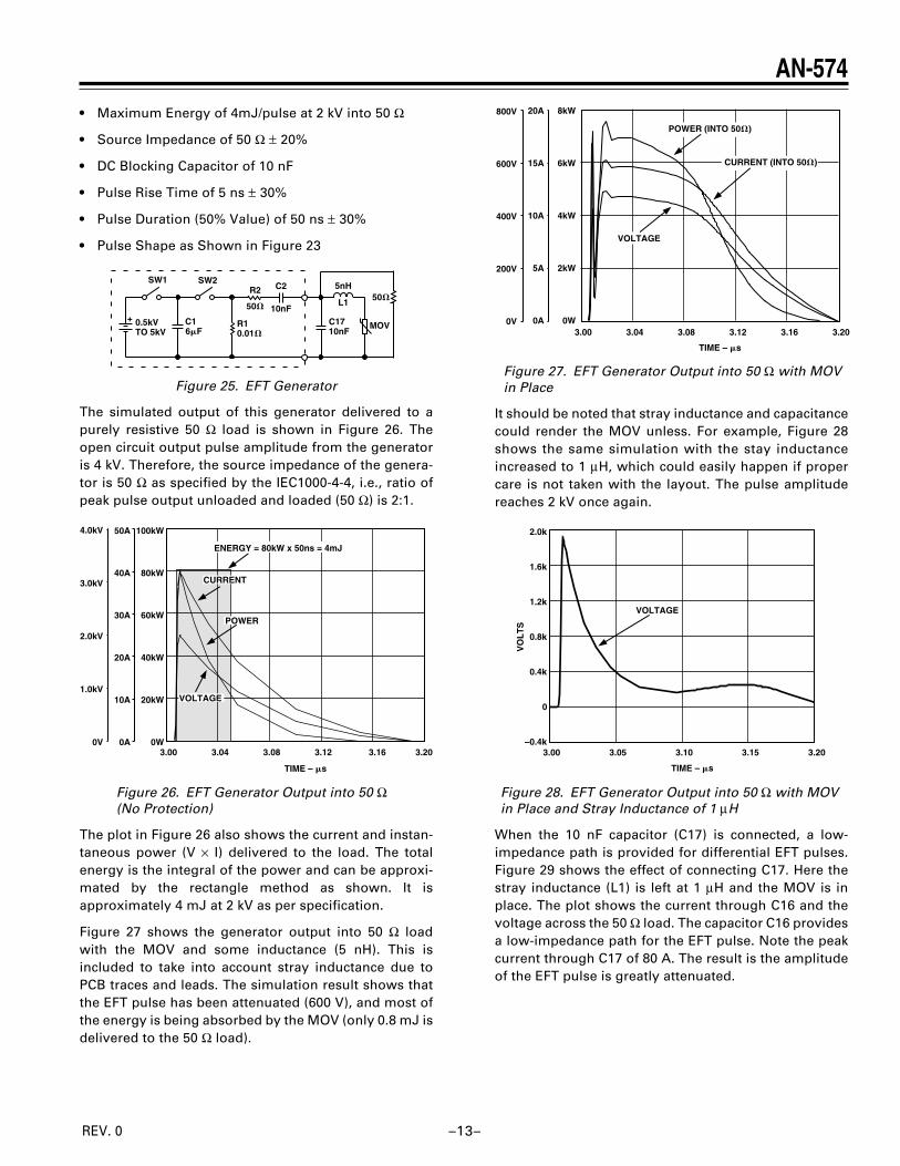
The simulated output of this generator delivered to apurely resistive 50 Ω load is shown in Figure 26. Theopen circuit output pulse amplitude from the generatoris 4 kV. Therefore, the source impedance of the genera-tor is 50 Ω as specified by the IEC1000-4-4, i.e., ratio ofpeak pulse output unloaded and loaded (50 Ω) is 2:1.
ENERGY = 80kW x 50ns = 4mJ
CURRENT
POWER
VOLTAGE
4.0kV
3.0kV
2.0kV
1.0kV
0V
50A
40A
30A
20A
10A
0A
100kW
80kW
60kW
40kW
20kW
0W3.00 3.04 3.08 3.12 3.16 3.20
TIME – s
Figure 26. EFT Generator Output into 50 Ω(No Protection)
The plot in Figure 26 also shows the current and instan-taneous power (V × I) delivered to the load. The totalenergy is the integral of the power and can be approxi-mated by the rectangle method as shown. It isapproximately 4 mJ at 2 kV as per specification.
Figure 27 shows the generator output into 50 Ω loadwith the MOV and some inductance (5 nH). This isincluded to take into account stray inductance due toPCB traces and leads. The simulation result shows thatthe EFT pulse has been attenuated (600 V), and most ofthe energy is being absorbed by the MOV (only 0.8 mJ isdelivered to the 50 Ω load).
800V
600V
400V
200V
0V
20A
15A
10A
5A
0A
8kW
6kW
4kW
2kW
0W3.00 3.04 3.08 3.12 3.16 3.20
TIME – s
CURRENT (INTO 50)
VOLTAGE
POWER (INTO 50)
Figure 27. EFT Generator Output into 50 Ω with MOVin Place
It should be noted that stray inductance and capacitancecould render the MOV unless. For example, Figure 28shows the same simulation with the stay inductanceincreased to 1 µH, which could easily happen if propercare is not taken with the layout. The pulse amplitudereaches 2 kV once again.
2.0k
1.6k
1.2k
0.8k
0.4k
0
–0.4k3.00 3.05 3.10 3.15 3.20
TIME – s
VOLTAGE
VO
LT
S
Figure 28. EFT Generator Output into 50 Ω with MOVin Place and Stray Inductance of 1 µH
When the 10 nF capacitor (C17) is connected, a low-impedance path is provided for differential EFT pulses.Figure 29 shows the effect of connecting C17. Here thestray inductance (L1) is left at 1 µH and the MOV is inplace. The plot shows the current through C16 and thevoltage across the 50 Ω load. The capacitor C16 providesa low-impedance path for the EFT pulse. Note the peakcurrent through C17 of 80 A. The result is the amplitudeof the EFT pulse is greatly attenuated.
–14–
AN-574
REV. 0
300V
200V
100V
0V
–100V
20A
0A
–20A
–40A
–60A
–80A3.0 3.2 3.4 3.6 3.8 4.0
TIME – s
CURRENT (INTO C17)
VOLTAGE (ACROSS 50 LOAD)
Figure 29. EFT Generator Output into 50 Ω with MOVand C17 (10 nF) in Place and Stray Inductance of 1 µH
IEC1000-4-5
The purpose of IEC1000-4-5 is to establish a commonreference for evaluating the performance of equipmentwhen subjected to high-energy disturbances on thepower and interconnect lines. Figure 30 shows a circuitwhich was used to generate the combinational wave(hybrid) pulse described in IEC1000-4-5. It is based onthe circuit shown in Figure 1 of IEC1000-4-5 (1995-02).Such a generator produces a 1.2/50 µs open-circuit volt-age, which is why it is referred to as a hybrid generator.The surge generator has an effective output impedanceof 2 Ω. This is defined as the ratio of peak open-circuitvoltage to peak short-circuit current.
R13.9
C120F
R1 L2SW1 SW2
0.5kVTO 4kV
+1.9 10H
5nH
MOVS20K275
R150
C1610nF
L1
Figure 30. Surge Generator (IEC1000-4-5)
Figure 31 shows the generator voltage and current out-put wave forms. The characteristics of the combinationwave generator are:
Open-Circuit Voltage:0.5 kV to at least 4.0 kVWaveform as shown in Figure 31Tolerance on open-circuit voltage is ±10%.
Short-Circuit Current:0.25 kA to 2.0 kAWaveform as shown in Figure 31Tolerance on short-circuit current is ±10%.
Repetition Rate of at Least 60 Seconds.
4kV
3kV
2kV
1kV
0V
2.0kA
1.5kA
1.0kA
0.5kA
0A0 20 40 60 80 100
TIME – s
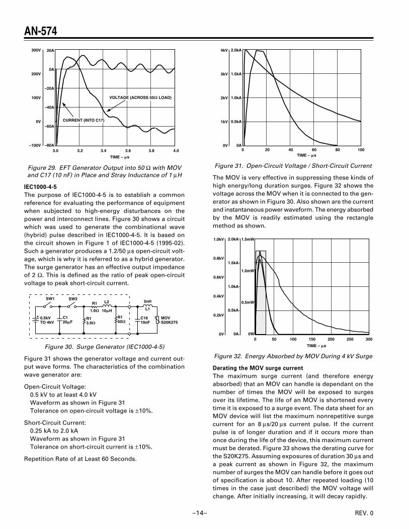
Figure 31. Open-Circuit Voltage / Short-Circuit Current
The MOV is very effective in suppressing these kinds ofhigh energy/long duration surges. Figure 32 shows thevoltage across the MOV when it is connected to the gen-erator as shown in Figure 30. Also shown are the currentand instantaneous power waveform. The energy absorbedby the MOV is readily estimated using the rectanglemethod as shown.
1.0kV
0.8kV
0.6kV
0.4kV
0.2kV
0V
2.0kA
1.5kA
1.0kA
0.5kA
0A
1.5mW
1.0mW
0.5mW
0W0 50 100 150 200 250 300
TIME – s
Figure 32. Energy Absorbed by MOV During 4 kV Surge
Derating the MOV surge current
The maximum surge current (and therefore energyabsorbed) that an MOV can handle is dependant on thenumber of times the MOV will be exposed to surgesover its lifetime. The life of an MOV is shortened everytime it is exposed to a surge event. The data sheet for anMOV device will list the maximum nonrepetitive surgecurrent for an 8 µs/20 µs current pulse. If the currentpulse is of longer duration and if it occurs more thanonce during the life of the device, this maximum currentmust be derated. Figure 33 shows the derating curve forthe S20K275. Assuming exposures of duration 30 µs anda peak current as shown in Figure 32, the maximumnumber of surges the MOV can handle before it goes outof specification is about 10. After repeated loading (10times in the case just described) the MOV voltage willchange. After initially increasing, it will decay rapidly.
–15–
AN-574
REV. 0
104
103
102
101
100
10–1
10 100 1k 10k
1x210102
103
104
105
106
8
Tr
I MA
X
s
SIOV-S20K275
SIEMENS MATSUSHITA COMPONENTS
Tr
IMAX
VAR0169-F
Figure 33. Derating Curve for S20K275
PCB DESIGN
Both susceptibility to conducted or radiated electromag-netic disturbances and analog performance wereconsidered at the PCB design stage. Fortunately many ofthe design techniques used to enhance analog andmixed-signal performance also lend themselves well toimproving the EMI robustness to the design. The keyidea is to isolate that part of the circuit which is sensitiveto noise and electromagnetic disturbances. Since theAD7751 carries out all the data conversion and signalprocessing, the robustness of the meter will be deter-mined to a large extent by how protected the AD7751 is.In order to ensure accuracy over a wide dynamic range,the data acquisition portion of the PCB should be kept asquiet as possible, i.e., minimal electrical noise. Noisewill cause inaccuracy in the analog-to-digital conversionprocess which takes place in the AD7751. One commonsource of noise in any mixed-signal system is theground return for the power supply. Here high-frequency noise (from fast edge rise times) can becoupled into the analog portion of the PCB by the com-mon impedance of the ground return path. Figure 34illustrates the mechanism.
GROUND
COMMONIMPEDANCE
Z
INOISE
VNOISE = INOISE x Z
ANALOG CIRCUITRY
DIGITAL CIRCUITRY
+ +
Figure 34. Noise Coupling via Ground Return Impedance
One common technique used to overcome these kindsof problems is to use separate analog and digital returnpaths for the supply. Also, every effort should be madeto keep the impedance of these return paths as low aspossible. In the PCB design for the AD7751, separateground planes were used to isolate the noisy groundreturns. The use of ground plane also ensures the imped-ance of the ground return path is kept very low. TheAD7751 and sensitive signal paths are located in a “quiet”part of the board which is isolated from the noisy ele-ments of the design like the power supply, flashing LED,etc. Since the PSU is capacitor-based, a substantialcurrent (approximately 35 mA at 240 V) will flow in theground return back to the phase wire (system ground).This is shown in Figure 30. By locating the PSU in thedigital portion of the PCB, this return current is keptaway from the AD7751 and analog input signals. Thiscurrent is at the same frequency as the signals beingmeasured and could cause accuracy issues (e.g., crosstalkbetween the PSU as analog inputs) if care is not takenwith the routing of the return current. In addition, part ofthe attenuation network for the Channel 2 (voltage chan-nel) is in the digital portion of the PCB. This helps toeliminate possible crosstalk to Channel 1 by ensuringanalog signal amplitudes are kept as low as possible inthe analog (“quiet”) portion of the PCB. Figure 35 showsthe PCB design which was eventually adopted for thewatt-hour meter.
AD7751
5V
EMIFILTER
35mA FROM PSU
ANALOGGROUND(QUIET)
DIGITALGROUND(NOISY)
AREAS ISOLATED WITHNO GROUND PRESENT
ON ANY LAYERGROUNDS CONNECTEDVIA FERRITE BEAD
240V
80V K5 K6
IN
OUT
CF
FAULT
K1
K2
Figure 35. AD7751 Watt-Hour Meter PCB Design
The partitioning of the power planes in the PCB designas shown in Figure 35 also allows us to implement theidea of a “moat” for the purposes of immunity to elec-tromagnetic disturbances. The digital portion of the PCBis the only place where both phase and neutral wires areconnected. This portion of the PCB contains the tran-sience suppression circuitry (MOV, ferrite, etc.) andpower supply circuitry. The ground planes are con-nected via a ferrite bead that helps to isolate the analogground from high frequency disturbances—see Designfor Immunity to Electromagnetic Disturbances section.
–16–
AN-574
REV. 0
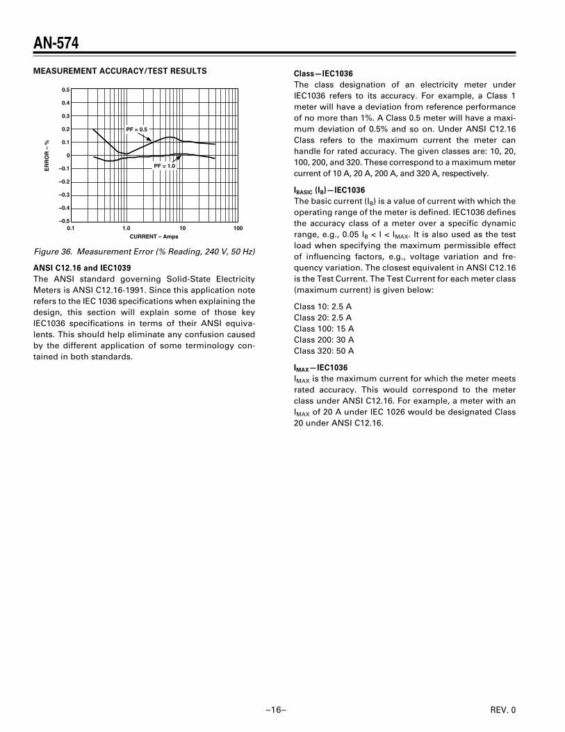
MEASUREMENT ACCURACY/TEST RESULTS
0.5
0.4
0.3
0.2
0.1
0
–0.1
–0.2
–0.3
–0.4
–0.5
ER
RO
R –
%
0.1 1.0 10 100
CURRENT – Amps
PF = 0.5
PF = 1.0
Figure 36. Measurement Error (% Reading, 240 V, 50 Hz)
ANSI C12.16 and IEC1039
The ANSI standard governing Solid-State ElectricityMeters is ANSI C12.16-1991. Since this application noterefers to the IEC 1036 specifications when explaining thedesign, this section will explain some of those keyIEC1036 specifications in terms of their ANSI equiva-lents. This should help eliminate any confusion causedby the different application of some terminology con-tained in both standards.
Class—IEC1036
The class designation of an electricity meter underIEC1036 refers to its accuracy. For example, a Class 1meter will have a deviation from reference performanceof no more than 1%. A Class 0.5 meter will have a maxi-mum deviation of 0.5% and so on. Under ANSI C12.16Class refers to the maximum current the meter canhandle for rated accuracy. The given classes are: 10, 20,100, 200, and 320. These correspond to a maximum metercurrent of 10 A, 20 A, 200 A, and 320 A, respectively.
IBASIC (IB)—IEC1036
The basic current (IB) is a value of current with which theoperating range of the meter is defined. IEC1036 definesthe accuracy class of a meter over a specific dynamicrange, e.g., 0.05 IB < I < IMAX. It is also used as the testload when specifying the maximum permissible effectof influencing factors, e.g., voltage variation and fre-quency variation. The closest equivalent in ANSI C12.16is the Test Current. The Test Current for each meter class(maximum current) is given below:
Class 10: 2.5 AClass 20: 2.5 AClass 100: 15 AClass 200: 30 AClass 320: 50 A
IMAX—IEC1036
IMAX is the maximum current for which the meter meetsrated accuracy. This would correspond to the meterclass under ANSI C12.16. For example, a meter with anIMAX of 20 A under IEC 1026 would be designated Class20 under ANSI C12.16.
–17–
AN-574
REV. 0
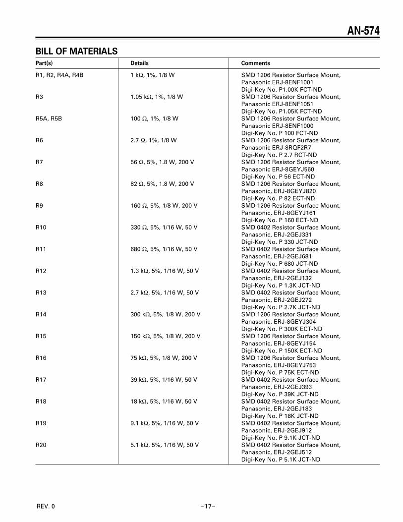
BILL OF MATERIALS
Part(s) Details Comments
R1, R2, R4A, R4B 1 kΩ, 1%, 1/8 W SMD 1206 Resistor Surface Mount,Panasonic ERJ-8ENF1001Digi-Key No. P1.00K FCT-ND
R3 1.05 kΩ, 1%, 1/8 W SMD 1206 Resistor Surface Mount,Panasonic ERJ-8ENF1051Digi-Key No. P1.05K FCT-ND
R5A, R5B 100 Ω, 1%, 1/8 W SMD 1206 Resistor Surface Mount,Panasonic ERJ-8ENF1000Digi-Key No. P 100 FCT-ND
R6 2.7 Ω, 1%, 1/8 W SMD 1206 Resistor Surface Mount,Panasonic ERJ-8RQF2R7Digi-Key No. P 2.7 RCT-ND
R7 56 Ω, 5%, 1.8 W, 200 V SMD 1206 Resistor Surface Mount,Panasonic ERJ-8GEYJ560Digi-Key No. P 56 ECT-ND
R8 82 Ω, 5%, 1.8 W, 200 V SMD 1206 Resistor Surface Mount,Panasonic, ERJ-8GEYJ820Digi-Key No. P 82 ECT-ND
R9 160 Ω, 5%, 1/8 W, 200 V SMD 1206 Resistor Surface Mount,Panasonic, ERJ-8GEYJ161Digi-Key No. P 160 ECT-ND
R10 330 Ω, 5%, 1/16 W, 50 V SMD 0402 Resistor Surface Mount,Panasonic, ERJ-2GEJ331Digi-Key No. P 330 JCT-ND
R11 680 Ω, 5%, 1/16 W, 50 V SMD 0402 Resistor Surface Mount,Panasonic, ERJ-2GEJ681Digi-Key No. P 680 JCT-ND
R12 1.3 kΩ, 5%, 1/16 W, 50 V SMD 0402 Resistor Surface Mount,Panasonic, ERJ-2GEJ132Digi-Key No. P 1.3K JCT-ND
R13 2.7 kΩ, 5%, 1/16 W, 50 V SMD 0402 Resistor Surface Mount,Panasonic, ERJ-2GEJ272Digi-Key No. P 2.7K JCT-ND
R14 300 kΩ, 5%, 1/8 W, 200 V SMD 1206 Resistor Surface Mount,Panasonic, ERJ-8GEYJ304Digi-Key No. P 300K ECT-ND
R15 150 kΩ, 5%, 1/8 W, 200 V SMD 1206 Resistor Surface Mount,Panasonic, ERJ-8GEYJ154Digi-Key No. P 150K ECT-ND
R16 75 kΩ, 5%, 1/8 W, 200 V SMD 1206 Resistor Surface Mount,Panasonic, ERJ-8GEYJ753Digi-Key No. P 75K ECT-ND
R17 39 kΩ, 5%, 1/16 W, 50 V SMD 0402 Resistor Surface Mount,Panasonic, ERJ-2GEJ393Digi-Key No. P 39K JCT-ND
R18 18 kΩ, 5%, 1/16 W, 50 V SMD 0402 Resistor Surface Mount,Panasonic, ERJ-2GEJ183Digi-Key No. P 18K JCT-ND
R19 9.1 kΩ, 5%, 1/16 W, 50 V SMD 0402 Resistor Surface Mount,Panasonic, ERJ-2GEJ912Digi-Key No. P 9.1K JCT-ND
R20 5.1 kΩ, 5%, 1/16 W, 50 V SMD 0402 Resistor Surface Mount,Panasonic, ERJ-2GEJ512Digi-Key No. P 5.1K JCT-ND

–18–
AN-574
REV. 0
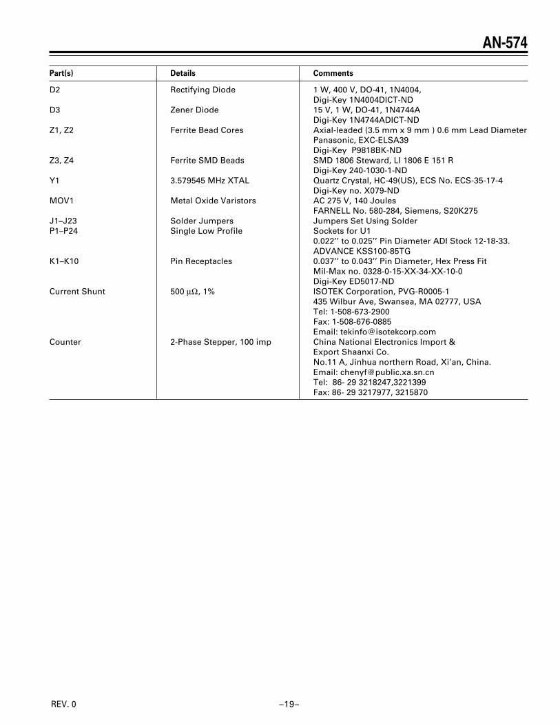
Part(s) Details Comments
R21 2.2 kΩ, 5%, 1/16 W, 50 V SMD 0402 Resistor Surface Mount,Panasonic, ERJ-2GEJ222Digi-Key No. P 2.2K JCT-ND
R22 1.2 kΩ, 5%, 1/16 W, 50 V SMD 0402 Resistor Surface Mount,Panasonic, ERJ-2GEJ122Digi-Key No. P 1.2K JCT-ND
R23 560 Ω, 5%, 1/16 W, 50 V SMD 0402 Resistor Surface Mount,Panasonic, ERJ-2GEJ561Digi-Key No. P 560 JCT-ND
R24, R25 330 kΩ, 5%, 1/2 W, 200 V SMD 2010 Resistor Surface Mount,Panasonic, ERJ-12ZY334Digi-Key No. P 330K WCT-ND
R26 470 Ω, 5%, 1 W Through-Hole, Panasonic,Digi-Key No. P470W-1BK-ND
R27, R28 10 kΩ, 5%, 1/8 W, 200 V SMD 1206 Resistor Surface Mount,Panasonic, ERJ-8GEYJ103Digi-Key No. P10K ECT-ND
R29, R30 820 Ω, 5%, 1/8 W, 200 V SMD 1206 Resistor Surface Mount,Panasonic, ERJ-8GEYJ821Digi-Key No. P 820 ECT-ND
R31, R32 20 Ω, 5%, 1/8 W, 200 V SMD 1206 Resistor Surface Mount,Panasonic, ERJ-8GEYJ200Digi-Key No. P 20 ECT-ND
R33 10 Ω, 5%, 1/8 W, 200 V SMD 1206 Resistor Surface Mount,Panasonic, ERJ-8GEYJ100Digi-Key No. P 10 ECT-ND
C1, C2, C3, C4, C5, C20, C21 33 nF, Multilayer Ceramic, 10% SMD 0805 Capacitor Surface Mount,50 V, X7R Panasonic, ECJ-2VB1H333K
Digi-Key No. PCC 1834 CT-NDC6, C14 10 µF, 6.3 V EIA Size A Capacitor Surface Chip-Cap,
Panasonic, ECS-TOJY106RDigi-Key No. PCS 1106CT-ND – 3.2 mm × 1.6 mm
C7, C8, C11, C13, C15, C16 100 nF, Multilayer Ceramic, SMD 0805 Capacitor Surface Mount,10%, 16 V, X7R Panasonic, ECJ-2VB1E104K
Digi-Key No. PCC 1812 CT-NDC9, C10 22 pF, Multilayer Ceramic, 5%, SMD 0402 Capacitor Surface Mount,
50 V, NPO Panasonic, ECU-E1H220JCQDigi-Key No. PCC 220CQCT-ND
C12 6.3 V, 220 µF, Electrolytic Through-Hole Panasonic, ECA-OJFQ221Digi-Key P5604 – NDD = 6.3 mm, H = 11.2 mm,Pitch = 2.5 mm, Dia. = 0.5 mm
C17 10 nF, 250 V, Class X2 Metallized Polyester FilmThrough-Hole Panasonic, ECQ-U2A103MNDigi-Key No. P4601-ND
C18 470 nF, 250 V AC Metallized Polyester FilmThrough-Hole Panasonic, ECQ-E6474KFDigi-Key No. EF6474-NP
C19 35 V, 470 µF, Electrolytic Through-Hole Panasonic, ECA-1VHG471Digi-Key P5554 – ND
U1 AD7755AN Supplied by ADI – 24-Pin DIP, Use Pin Receptacles(P1–P24)
U2 LM78L05 National Semiconductor, LM78L05ACM, S0-8Digi-Key LM78L05ACM-ND
U3 PS2501-1 Opto, NEC, Digi-key No. PS2501-1NEC-NDD1, D4 Low-Current LED HP HLMP-D150
Newark 06F6429 (Farnell 323-123)
–19–
AN-574
REV. 0
Part(s) Details Comments
D2 Rectifying Diode 1 W, 400 V, DO-41, 1N4004,Digi-Key 1N4004DICT-ND
D3 Zener Diode 15 V, 1 W, DO-41, 1N4744ADigi-Key 1N4744ADICT-ND
Z1, Z2 Ferrite Bead Cores Axial-leaded (3.5 mm x 9 mm ) 0.6 mm Lead DiameterPanasonic, EXC-ELSA39Digi-Key P9818BK-ND
Z3, Z4 Ferrite SMD Beads SMD 1806 Steward, LI 1806 E 151 RDigi-Key 240-1030-1-ND
Y1 3.579545 MHz XTAL Quartz Crystal, HC-49(US), ECS No. ECS-35-17-4Digi-Key no. X079-ND
MOV1 Metal Oxide Varistors AC 275 V, 140 JoulesFARNELL No. 580-284, Siemens, S20K275
J1–J23 Solder Jumpers Jumpers Set Using SolderP1–P24 Single Low Profile Sockets for U1
0.022’’ to 0.025’’ Pin Diameter ADI Stock 12-18-33.ADVANCE KSS100-85TG
K1–K10 Pin Receptacles 0.037’’ to 0.043’’ Pin Diameter, Hex Press FitMil-Max no. 0328-0-15-XX-34-XX-10-0Digi-Key ED5017-ND
Current Shunt 500 µΩ, 1% ISOTEK Corporation, PVG-R0005-1435 Wilbur Ave, Swansea, MA 02777, USATel: 1-508-673-2900Fax: 1-508-676-0885Email: [email protected]
Counter 2-Phase Stepper, 100 imp China National Electronics Import &Export Shaanxi Co.No.11 A, Jinhua northern Road, Xi’an, China.Email: [email protected]: 86- 29 3218247,3221399Fax: 86- 29 3217977, 3215870
–20–
AN-574
REV. 0
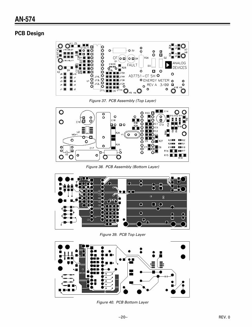
PCB Design
Figure 37. PCB Assembly (Top Layer)
Figure 38. PCB Assembly (Bottom Layer)
Figure 39. PCB Top Layer
Figure 40. PCB Bottom Layer
–21–
AN-574
REV. 0
K2
K4
K3
K1
K5
K6
K8
K9
K10
SEESCHEMATIC 2
SEESCHEMATIC 2
U1AD7751
K7
1 2Z3 VAL R5A
100
J22
R11k
C200.033F
C10.033F
R31.05k
C30.033FR6
2.7R756
CALV1BHI
CALV1BLO R41k
C20.033F
1 2Z4 VAL R5B
100
J23
C210.033F
CALHI CALLOW
R24330k
R25330k
R4A1k
C40.033F
R4B1k
C50.033F
1 2Z1 VAL
C1B0.47F
R26470
MOV1140J
C170.01F
D2IN4004
D3IN4744
C19470F
35V
G1 G2 G3 G4
VIN VOUT
U2 7805
1 2Z2 VAL
2 3 6 7
18 5VVDD
VDD
R2710k
C70.1F
C610F6.3V
+
+
1
2
3
4
5
6
7
8
9
10
11
12
24
23
22
21
20
19
18
17
16
15
14
13
C1410F6.3V
+ C130.1F
C12220F6.3V
+
C110.1F
R3310 R32
20
C150.1F
C160.1FR31
20
R30820
D1HLMPD150
1
2
U3
PS2501
4
3
D2HLMPD150
R29
820
C1022pF
Y13.579545MHz
J15
J14
J13
J12
J11
J15L
0J14L
0
J13L
0J12L
0
J11L
0
J15H
0J14H
0
J13H
0J12H
0
J11H
0
R2810k
C80.1F
VDD
VDD
C922pF
DVDD
AC/DC
AVDD
V1A
V1B
V1N
V2N
V2P
RESET
REF
AGND
SCF
F1
F2
CF
DGND
REVP
FAULT
CLKOUT
CLKIN
G0
G1
S0
S1
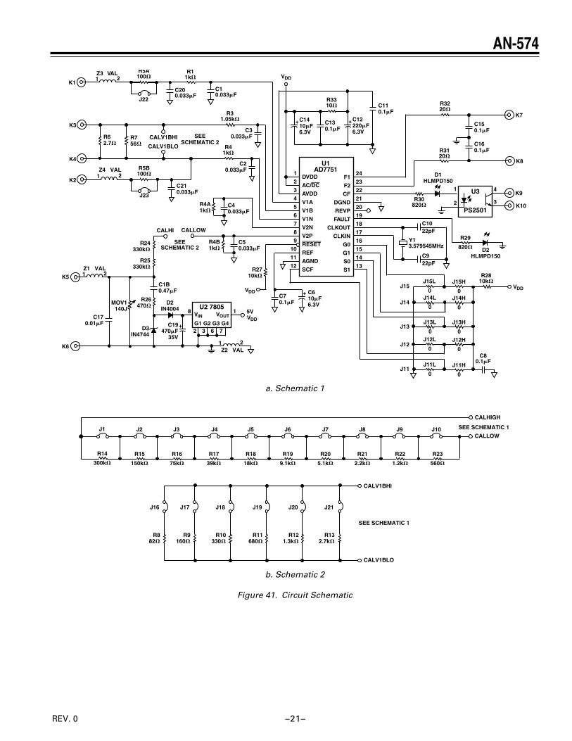
a. Schematic 1
SEE SCHEMATIC 1
J1
R14
300k
J2
R15
150k
J3
R16
75k
J4
R17
39k
J5
R18
18k
J6
R19
9.1k
J7
R20
5.1k
J8
R21
2.2k
J9
R22
1.2k
J10
R23
560
CALHIGH
CALLOW
SEE SCHEMATIC 1
J16
R882
J17
R9160
J18
R10330
J19
R11680
J20
R121.3k
J21
R132.7k
CALV1BHI
CALV1BLO
b. Schematic 2
Figure 41. Circuit Schematic

–22–

–23–

PR
INT
ED
IN U
.S.A
.E
0195
5–2.
5–6/
01(0
)
–24–