
A Switched VCO-based CMOS UWB Transmitter for 3 … · ... Kwangwoon University, Seoul, ... 3...
7
JOURNAL OF SEMICONDUCTOR TECHNOLOGY AND SCIENCE, VOL.17, NO.3, JUNE, 2017 ISSN(Print) 1598-1657 https://doi.org/10.5573/JSTS.2017.17.3.326 ISSN(Online) 2233-4866 Manuscript received Mar. 15, 2016; accepted Jun. 11, 2017 1 School of Department of Electronic Engineering, Kwangwoon University, Seoul, Korea 2 Korea Electronics Technology Institute, Seongnam, Korea 3 School of Department of Electronics and Communications Engineering, Kwangwoon University, Seoul, Korea E-mail : [email protected] A Switched VCO-based CMOS UWB Transmitter for 3-5 GHz Radar and Communication Systems Woon-Sung Choi 1 , Myung-Chul Park 2 , Hyuk-Jun Oh 3 , and Yun-Seong Eo 1,* Abstract—A switched VCO-based UWB transmitter for 3-5 GHz is implemented using 0.18 μm CMOS technology. Using RF switch and timing control of DPGs, the uniform RF power and low power consumption are possible regardless of carrier frequency. And gate control of RF switch enables the undesired side lobe rejection sufficiently. The measured pulse width is tunable from 0.5 to 2 ns. The measured energy efficiency per pulse is 4.08% and the power consumption is 0.6 mW at 10 Mbps without the buffer amplifier. Index Terms—Switched VCO-based UWB transmitter, CMOS RFIC, impulse generator, side lobe rejection, low power transmitter I. INTRODUCTION The Impulse Radio (IR)-Ultra Wide Band (UWB) system has the advantages of high resolution and coexistence with the other radio signals so that there have been many reports dealing with the radar sensor and location based systems (LBS). The allowed band includes 3-5 GHz and 6-10 GHz and the maximum available power spectral density is under -41.3 dBm/MHz in average. Moreover, the transmitted power spectrum meets the required spectrum mask given from FCC regulation. Concerning with the transmitter of IR-UWB transceiver, the digitally synthesized topologies and the switched VCO types have been recently reported [1-7]. The carrier-free digitally synthesized one has some drawbacks such as the undesired digital noise and much more side lobe due to the waveform shape while it has the merit of inductorless small chip area and low power consumption. On the other hand, the switched VCO type has the stable oscillation in the actual design and the accurate frequency trimming is possible with the varactor and capacitor control. Main issues of the switched VCO UWB transmitter include the power consumption and the RF power leakage of the VCO [1]. And another issue of the switched VCO UWB transmitter is the different start- up time for the different carrier frequency [7]. The different start-up time produces the different and limited amplitude of the UWB impulse for each band. In this work, LC VCO with on-off current source is employed to save the current consumption during the intervals between two consecutive impulses, and the RF switch placed at the VCO output enables to provide the equal amplitudes in cost of a little more current consumption. On the other hands, the side lobe of UWB impulse signal is also important problem of UWB transmitter. Although there are many UWB transmitters adopting the pulse-shaping method such as Gaussian- shaping, a simple pulse shaping technique is used here using a RF switch controlled by the switching pulse of variable rising and falling times. The achieved side band rejection is sufficient to be compliant with the desired spectrum mask. Comparing with our previous 7-9 GHz UWB transmitter [8], 3-5 GHz IR-UWB transmitter is fabricated in 0.18 um CMOS technology and the analysis on the timing and side-lobe rejection is also presented.
Transcript of A Switched VCO-based CMOS UWB Transmitter for 3 … · ... Kwangwoon University, Seoul, ... 3...

JOURNAL OF SEMICONDUCTOR TECHNOLOGY AND SCIENCE, VOL.17, NO.3, JUNE, 2017 ISSN(Print) 1598-1657 https://doi.org/10.5573/JSTS.2017.17.3.326 ISSN(Online) 2233-4866
Manuscript received Mar. 15, 2016; accepted Jun. 11, 2017 1 School of Department of Electronic Engineering, Kwangwoon University, Seoul, Korea 2 Korea Electronics Technology Institute, Seongnam, Korea 3 School of Department of Electronics and Communications Engineering, Kwangwoon University, Seoul, Korea E-mail : [email protected]
A Switched VCO-based CMOS UWB Transmitter for 3-5 GHz Radar and Communication Systems
Woon-Sung Choi1, Myung-Chul Park2, Hyuk-Jun Oh3, and Yun-Seong Eo1,*
Abstract—A switched VCO-based UWB transmitter for 3-5 GHz is implemented using 0.18 μm CMOS technology. Using RF switch and timing control of DPGs, the uniform RF power and low power consumption are possible regardless of carrier frequency. And gate control of RF switch enables the undesired side lobe rejection sufficiently. The measured pulse width is tunable from 0.5 to 2 ns. The measured energy efficiency per pulse is 4.08% and the power consumption is 0.6 mW at 10 Mbps without the buffer amplifier. Index Terms—Switched VCO-based UWB transmitter, CMOS RFIC, impulse generator, side lobe rejection, low power transmitter
I. INTRODUCTION
The Impulse Radio (IR)-Ultra Wide Band (UWB) system has the advantages of high resolution and coexistence with the other radio signals so that there have been many reports dealing with the radar sensor and location based systems (LBS). The allowed band includes 3-5 GHz and 6-10 GHz and the maximum available power spectral density is under -41.3 dBm/MHz in average. Moreover, the transmitted power spectrum meets the required spectrum mask given from FCC regulation. Concerning with the transmitter of IR-UWB
transceiver, the digitally synthesized topologies and the switched VCO types have been recently reported [1-7]. The carrier-free digitally synthesized one has some drawbacks such as the undesired digital noise and much more side lobe due to the waveform shape while it has the merit of inductorless small chip area and low power consumption. On the other hand, the switched VCO type has the stable oscillation in the actual design and the accurate frequency trimming is possible with the varactor and capacitor control. Main issues of the switched VCO UWB transmitter include the power consumption and the RF power leakage of the VCO [1]. And another issue of the switched VCO UWB transmitter is the different start-up time for the different carrier frequency [7]. The different start-up time produces the different and limited amplitude of the UWB impulse for each band.
In this work, LC VCO with on-off current source is employed to save the current consumption during the intervals between two consecutive impulses, and the RF switch placed at the VCO output enables to provide the equal amplitudes in cost of a little more current consumption. On the other hands, the side lobe of UWB impulse signal is also important problem of UWB transmitter. Although there are many UWB transmitters adopting the pulse-shaping method such as Gaussian-shaping, a simple pulse shaping technique is used here using a RF switch controlled by the switching pulse of variable rising and falling times. The achieved side band rejection is sufficient to be compliant with the desired spectrum mask. Comparing with our previous 7-9 GHz UWB transmitter [8], 3-5 GHz IR-UWB transmitter is fabricated in 0.18 um CMOS technology and the analysis on the timing and side-lobe rejection is also presented.
JOURNAL OF SEMICONDUCTOR TECHNOLOGY AND SCIENCE, VOL.17, NO.3, JUNE, 2017 327
II. TRANSMITTER ARCHITECTURE AND
TIMING
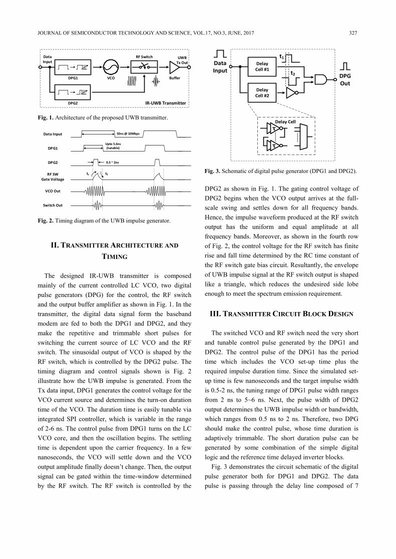
The designed IR-UWB transmitter is composed mainly of the current controlled LC VCO, two digital pulse generators (DPG) for the control, the RF switch and the output buffer amplifier as shown in Fig. 1. In the transmitter, the digital data signal form the baseband modem are fed to both the DPG1 and DPG2, and they make the repetitive and trimmable short pulses for switching the current source of LC VCO and the RF switch. The sinusoidal output of VCO is shaped by the RF switch, which is controlled by the DPG2 pulse. The timing diagram and control signals shown is Fig. 2 illustrate how the UWB impulse is generated. From the Tx data input, DPG1 generates the control voltage for the VCO current source and determines the turn-on duration time of the VCO. The duration time is easily tunable via integrated SPI controller, which is variable in the range of 2-6 ns. The control pulse from DPG1 turns on the LC VCO core, and then the oscillation begins. The settling time is dependent upon the carrier frequency. In a few nanoseconds, the VCO will settle down and the VCO output amplitude finally doesn’t change. Then, the output signal can be gated within the time-window determined by the RF switch. The RF switch is controlled by the
DPG2 as shown in Fig. 1. The gating control voltage of DPG2 begins when the VCO output arrives at the full-scale swing and settles down for all frequency bands. Hence, the impulse waveform produced at the RF switch output has the uniform and equal amplitude at all frequency bands. Moreover, as shown in the fourth row of Fig. 2, the control voltage for the RF switch has finite rise and fall time determined by the RC time constant of the RF switch gate bias circuit. Resultantly, the envelope of UWB impulse signal at the RF switch output is shaped like a triangle, which reduces the undesired side lobe enough to meet the spectrum emission requirement.
III. TRANSMITTER CIRCUIT BLOCK DESIGN
The switched VCO and RF switch need the very short and tunable control pulse generated by the DPG1 and DPG2. The control pulse of the DPG1 has the period time which includes the VCO set-up time plus the required impulse duration time. Since the simulated set-up time is few nanoseconds and the target impulse width is 0.5-2 ns, the tuning range of DPG1 pulse width ranges from 2 ns to 5~6 ns. Next, the pulse width of DPG2 output determines the UWB impulse width or bandwidth, which ranges from 0.5 ns to 2 ns. Therefore, two DPG should make the control pulse, whose time duration is adaptively trimmable. The short duration pulse can be generated by some combination of the simple digital logic and the reference time delayed inverter blocks.
Fig. 3 demonstrates the circuit schematic of the digital pulse generator both for DPG1 and DPG2. The data pulse is passing through the delay line composed of 7
Buffer
DPG2
DPG1 VCO
IR-UWB Transmitter
RF SwitchDataInput
UWB Tx Out
Fig. 1. Architecture of the proposed UWB transmitter.
VCO Out
DPG1
Switch Out
DPG2
RF SWGate Voltage
0.5 ~ 2ns
Upto 5.6ns(tunable)
50ns @ 10Mbps
tr tf
Data Input
Fig. 2. Timing diagram of the UWB impulse generator.
τ
τ
Delay Cell
DelayCell #2
DelayCell #1
DataInput
DPG Out
t1
t2
Fig. 3. Schematic of digital pulse generator (DPG1 and DPG2).

328 WOON-SUNG CHOI et al : A SWITCHED VCO-BASED CMOS UWB TRANSMITTER FOR 3-5 GHZ RADAR AND …
unit delay cells. Each unit delay cell consists of 2 inverters and produces the unit time delay, which is 3-bit digitally trimmable by adjusting the current source of the inverter cell. As shown in Fig. 3, from the cascaded inverter chain, the 8 different-delay digital pulses are generated and one of them is selected by the 3-bits MUX. The resultant values of time delay t1 and t2 as shown in Fig. 3 are approximately 0, 2∆td, ···, 7∆td, where ∆td is the tunable time delay of the unit delay cell. The outputs of two delay cells are used as the input of AND gate for the digital pulse generation. Since the DPG output pulse has the duration of t2-t1=k∆td (k=0, 1, 2, ···, 7) and ∆td is variable from 0.15 ns to 0.8 ns by controlling the inverter current, the pulse width of the DPG can be tuned from 0.15 ns to 5.6 ns. On the other hand, since DPG2 is used for RF switch and determines the UWB impulse width or bandwidth it needs only the time duration range of 0.5 ~ 2 ns, which can be easily obtained by our DPG circuit.
Concerning with the oscillator core, a differential cross coupled LC VCO topology with the digitally switched capacitor bank is employed as the impulse generator as illustrated in Fig. 4. The resonance frequency of LC tank determines the UWB carrier frequency, which sweep over 3-5 GHz. The DPG1 output is used as the control voltage to turn on the NMOS (M3) switch, which is connected in series with the tail current source of the VCO core. Since the control signal is injected into the NMOS switch, not into the current source itself, the set-up time depends on the gate capacitance of MOS switch size and the VCO current are independently optimized. According to [7], the start-up transient response of the oscillator output is derived and the resultant equation
indicates that the VCO output amplitude depends on the carrier frequency and settling time is shorter at higher frequency. In order to solve these problems, the time widow of DPG2 pulse is tunable and located after the VCO output settles down sufficiently, in cost of the slightly more power consumption due to the additional turn-on time of VCO.
Because the impulse is gated after the VCO reaches its stable region for all frequency bands, the equal amplitude can be obtained for each band. And concerning with the side lobe rejection, as shown in Fig. 5, the gate voltage of the RF switch has some slope of the rise and fall transitions using the resistor RS, which is connected n series at the gate. Hence it makes the finite rise and fall times (0.25-1 ns) of the gate voltage determined by RC time constant. The C is the gate capacitance Cgs and the resistor RS is digitally trimmable. The finite rise and fall times of the gate control voltage result in the impulse envelop like the triangular form, and thus reduce the side lobe consequently. The RF switch consists of series-shunt configuration to enhance the isolation and suppress the undesired pulse following the main impulse. Fig. 5 depicts the schematic of the RF switch and gate control circuit.
The final buffer amplifier should isolate the VCO resonator core from the low 50 ohm output load and also drive it. The inverter-like push-pull CMOS amplifier is employed because of its convenient power matching over the 3-5 GHz band only with a few off-chip LC components. Fig. 6 shows the simulation results of the designed UWB transmitter. The DPG1 pulse turns on the VCO, and then the oscillation begins. In order to generate the DPG2 pulse after VCO is settled down, delay cell of DPG 2 selected according to the carrier frequency. Fig. 7 and 8 show the output simulation
Fig. 4. LC VCO schematic with digitally trimmed capacitor.
Fig. 5. Schematic of RF switch and gate control circuit.

JOURNAL OF SEMICONDUCTOR TECHNOLOGY AND SCIENCE, VOL.17, NO.3, JUNE, 2017 329
results for pulse shape of the RF SW gate gate control voltage in time domain and frequency domain. Rectangular pulse of Fig. 7(a) is transformed to sinc function waveform in frequency domain and the waveform has several side lobe such as a dotted line in Fig. 8. Through optimizing the resistance of the gate control circuit shown in Fig. 7(b), undesired side lobe is rejected such as solid line of Fig. 8.
IV. MEASUREMENT RESULTS
The switched VCO based UWB transmitter is implemented in 0.18 μm CMOS technology and measured. The modulation for the measurement is on-off keying (OOK) with 10 Mb/s RZ data. Fig. 9 and 10 show the measured UWB impulse spectrum and waveforms at the buffer output for each band and bandwidth, which is measured using power spectrum analyzer (Agilent
Fig. 6. Simulation results of designed UWB transmitter.
-2 0 2 4 6 8-0.5
0.0
0.5
1.0
1.5
2.0
Ampl
itude
(V)
Time (ns)
RF SW gate voltage
Tx OUTR = 0
(a)
-2 0 2 4 6 8-0.5
0.0
0.5
1.0
1.5
2.0
R = ROPT
Ampl
itude
(V)
Time (ns)
RF SW gate voltage
Tx OUT
(b)
Fig. 7. Simulation result of output pulse and gate control voltage in time domain (a) R = 0, (b) R= ROPT.
Fig. 8. Simulation result of output pulse in frequency domain.
Fig. 9. Measured power spectrum of UWB transmitter with spectrum mask.
330 WOON-SUNG CHOI et al : A SWITCHED VCO-BASED CMOS UWB TRANSMITTER FOR 3-5 GHZ RADAR AND …
E4440A) and digital signal oscilloscope (Agilent 54855A). The measured pulse duration is variable from 0.5 to 2 ns.
The peak amplitude of the output voltage is about 560 mVPP. The UWB transmitter has the equal powers for the three sub-band and is also compliant with FCC mask in the range of 3-5 GHz at 10 Mbps data input. The
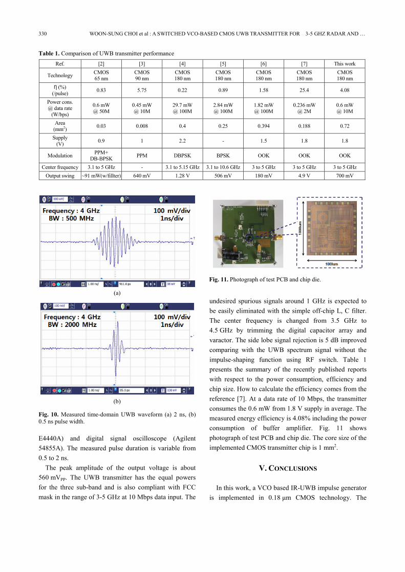
undesired spurious signals around 1 GHz is expected to be easily eliminated with the simple off-chip L, C filter. The center frequency is changed from 3.5 GHz to 4.5 GHz by trimming the digital capacitor array and varactor. The side lobe signal rejection is 5 dB improved comparing with the UWB spectrum signal without the impulse-shaping function using RF switch. Table 1 presents the summary of the recently published reports with respect to the power consumption, efficiency and chip size. How to calculate the efficiency comes from the reference [7]. At a data rate of 10 Mbps, the transmitter consumes the 0.6 mW from 1.8 V supply in average. The measured energy efficiency is 4.08% including the power consumption of buffer amplifier. Fig. 11 shows photograph of test PCB and chip die. The core size of the implemented CMOS transmitter chip is 1 mm2.
V. CONCLUSIONS
In this work, a VCO based IR-UWB impulse generator is implemented in 0.18 μm CMOS technology. The
Table 1. Comparison of UWB transmitter performance
Ref. [2] [3] [4] [5] [6] [7] This work
Technology CMOS 65 nm
CMOS 90 nm
CMOS 180 nm
CMOS 180 nm
CMOS 180 nm
CMOS 180 nm
CMOS 180 nm
Ƞ (%) (/pulse) 0.83 5.75 0.22 0.89 1.58 25.4 4.08
Power cons. @ data rate
(W/bps)
0.6 mW @ 50M
0.45 mW @ 10M
29.7 mW @ 100M
2.84 mW @ 100M
1.82 mW @ 100M
0.236 mW @ 2M
0.6 mW @ 10M
Area (mm2) 0.03 0.008 0.4 0.25 0.394 0.188 0.72
Supply (V) 0.9 1 2.2 - 1.5 1.8 1.8
Modulation PPM+ DB-BPSK PPM DBPSK BPSK OOK OOK OOK
Center frequency 3.1 to 5 GHz - 3.1 to 5.15 GHz 3.1 to 10.6 GHz 3 to 5 GHz 3 to 5 GHz 3 to 5 GHz Output swing ~91 mW(w/fillter) 640 mV 1.28 V 506 mV 180 mV 4.9 V 700 mV
(a)
(b)
Fig. 10. Measured time-domain UWB waveform (a) 2 ns, (b) 0.5 ns pulse width.
Fig. 11. Photograph of test PCB and chip die.

JOURNAL OF SEMICONDUCTOR TECHNOLOGY AND SCIENCE, VOL.17, NO.3, JUNE, 2017 331
transmitter carrier frequency range is 3.0 to 5.0 GHz. The RF switch and proposed digital pulse generator enable us to achieve the tunable impulse width and suppress the undesired side lobe. The transmitter shows that the energy efficiency per pulse is 4.08% and meets the regulated spectrum mask for each sub-band.
ACKNOWLEDGMENTS
This work has been supported by the Research Grant of Kwangwoon University in 2015 and also supported by ICT R&D Program of MSIP/IITP [14-911-01-001, Development of Quasi-Millimeter-Wave Channel-Adaptive Antennas and Transceivers.
REFERENCES
[1] R. Xu, Y. Jin, and C. Nguyen, “Power-Efficienct Switching-Based CMOS UWB Transmitter for UWB Communications and Radar Systems,” Micro. Theory Tech, 2006. IEEE Transactions on, Vol.54, No. 8, pp. 3271-3277, Aug., 2006.
[2] Y. Park, D.D. Wentzloff, “An All-Digital 12 pJ/Pulse IR-UWB Transmitter Synthesized From a Standard Cell Library” Solid-State Circuits, IEEE Journal of, Vol.46, No.5, pp.1147-1157, May., 2011.
[3] D.D. Wentzloff and A. P. Chandrakasan, “A 47 pJ/pulse 3.1 to 5 GHz All-Digital UWB Transmitter in 90nm CMOS,” Solid-State Circuits, IEEE International Conference on, 11-15, pp.118-119, Feb., 2007.
[4] T. Norimatsu, R. Fujiwara, M. Miyazaki, Y. Ogata, S. Kobayashi, N. Koshizuka, and K. Sakamura “A UWB-IR Trasnmitter with Digitally Controlled Pulse Generator,” Solid-State circuits, IEEE Journal of, Vol.42, No.6, pp.1300-1309, Jun., 2007.
[5] X. Wang, S. Fan, H. Tang, L. Lin, J.Liu, Q. Fang, H.Zhao, A. Wang, L. Yang, and B. Zhao, “A Whole-Chip ESD-Protected 0.14pJ/p-mV 3.1-10.6 GHz Impulse-Radio UWB Transmitter in 0.18um CMOS,” Micro. Theory Tech, 2011. IEEE Transactions on, Vol.59, No. 4, pp. 1109-1116, Apr., 2011.
[6] T. A. Phan, J. Lee, V. Krizhanovskii, S. K. Han, and S. G. Lee, “A 18pJ/pulse OOK CMOS
Transmitter for Multiband UWB Impulse Radio,” Micro. Theory Tech, 207. IEEE Transactions on, Vol.17, No. 9, pp. 688-690, Sep., 2007..
[7] S. Diao, Y. Zheng, and C. Heng, “A CMOS Ultra Low-Power and Highly Efficient UWB-IR Transmitter for WPAN Applications,” Circuits and Systems II, IEEE Transactions on, Vol.56, No.3, pp.200-204, Mar., 2009.
[8] Y. Eo, M. Park and M. Ha, “A 6.5 - 8.5 GHz CMOS UWB Transmitter Using Switched LC VCO”, Journal of Semiconductor Technology and Science, vol. 15, no. 3, pp. 417-422, 2015.
Woon Sung Choi received the B.S., M.S degrees in Electronics Engi- neering from Kwangwoon University, Korea, in 2012, 2014, respectively. Since 2014, he has been toward the Ph.D. degree at the same university. His research interests include CMOS
RFIC design for radar system.
Myung Chul Park received the B.S., M.S., and Ph.D. degrees in Elec- tronics Engineering from Kwang- woon University, Korea, in 2011, 2013, 2016, respectively. Since 2016, he joined Korea Electronics Tech- nology Institute, Korea. His research
interests include IoT platform and relevant RF RF/analog circuit and system design.
Hyuk Jun Oh received his Ph.D., M.S., B.S., degrees in Electrical Engineering from KAIST (Korea Advanced Institute of Technology), Deajeon, The Republic of Korea, in 1999, 1995, and 1993, respectively. He is a professor of the Department
of Electrical Communications Engineering at Kwang- woon University, Seoul, The Republic of Korea. From 2001 to 2004, he worked on 3GPP MSM development at Qualcomm Inc., USA. His area of research includes VLSI signal processing wireless communication system, and radar signal processing.

332 WOON-SUNG CHOI et al : A SWITCHED VCO-BASED CMOS UWB TRANSMITTER FOR 3-5 GHZ RADAR AND …
Yun Seong Eo received the B.S., M.S., and Ph. D degrees in Electrical Engineering all from Korea Advanced Institute of Science and Technology (KAIST), Daejeon, Korea, in 1993, 1995 and 2001, respectively. From 2000 to 2002, he
has with LG Electronics Institute of Technology, Seoul, Korea, where he was involved in designing RF integrated circuit (RFICs) such as VCO, LNA, and PA using InGaP HBT devices. In September 2002, he joined Samsung Advanced Institute of Technology, Yongin, Korea, where he developed 5-GHz CMOS PA and RF transceivers for 802.11n target, and was also involved in the development of 900 MHz RF identification (RFID) and 2.4-GHz ZigBee RF transceivers. In September 2005, he joined Kwangwoon University, Seoul, Korea, where he is currently a professor with Electronics Engineering department During the recent 10 years, he developed so many CMOS RF transceiver ICs for the various applications such as WPAN UWB/ZigBee, T-DMB, DVB-H, WiFi, and Cognitive Radio. And recently, he is also focusing on CMOS UWB and FMCW Radar ICs for surveillance system and proximity fusing. In 2009, he founded Silicon R&D Inc, where he is CEO and develops CMOS based UWB radar ICs and low power/low rate RFICs.


