A Surface-Mount Technology Primer-Part 7 - n5dux.comn5dux.com/ham/files/pdf/Surface-Mount Technology...
8
A Surface-Mount Technology Primer-Part 7 What makes today's compact electronics gear possible? SMT. By Bryan P. Bergeron, NUlN 30 Gardner Road. Apt 1G Brookline. MA 02146 The most obvious difference between traditional and surface-mount (SM) components is size. Note the relative sizes of the stamp, a conventional TO-92case transistor on the left, and the three SM transistors on the right. Of the three SM transistors, the largest-about 4.5 x 2.5 x 1.5 mrn-(in an SOT-89 package) is a general-purpose NPN silicon tran- sistor, with a Voo of 90 V and a PI, of 1 W. The two smaller SM transistors (in SOT-23 packages) are general-purpose PNP silicon devices with a VcBo of 80 V and a Po of 200 mW. H ow do manufacturers of amateur communications equipment manage to consistently offer trace can handle only about 1 A.~ Even ing. SMT employs solder to provide elec- products that provide more features, in the width of traces carrying only small sig- trical and mechanical connections between smaller packages, with each new model? In nals cannot be reduced indefinitely. In- components and PC board^.^ See Tables 1 part, this progress has been achieved creased path resistance-along with the and 2 for a summary of the benefits and through the judicious use of surface-mount crosstalk associated with more closely limitations of SMT. devices (SMDs). SMDs provide not only spaced traces-can render a circuit in- Many equipment manufacturers enter significant size and weight advantages over operable. the SMT field by making mixed-technology conventional components, but are also Similarly, increasing circuit density by boards-PC boards that contain SMDs and more easily handled by automated using more circuit-board layers has practi- conventional devices (see Fig I).' Mixed manufacturing systems, resulting in lower cal limits. Not only do costs increase as technology, or underside attachment of manufacturing costs. layers are added, but board thickness and SMDs, has been used for almost 25 years Amateurs interested in designing or weight begin to get out of hand when more in Japan to reduce the size and cost of elec- maintaining their own communications than 12 layers are used. tronic product^.^ This approach is also equipment should know something about especially attractive to amateurs who would surface-mount technology (SMT).' In this Surface-Mount Tmhnology article, 1'11 introduce you to SMT and Although SMT has received a great deal SMDs. In Part 2, I'll discuss some of the of attention lately, the surface mounting of practical aspects of working with SMDs. components dates back to the hybrid assemblies of the late 1950s.' SMT was Smaller, Tighter, Cheaper not fully exploited until the 1980s, however, Evolution in PC-board technology when circuit complexity reached the point centers around developing different board that through-hole component-mounting compositions, producing thinner and more- techniques were no longer economically or exactly positioned traces, and minimizing technologically feasible. Faced with the production costs. The demand for denser limitations of conventional PC-board tech- electronic assemblies has pushed conven- nology, circuit-design engineers turned to tional PC-board technology to its limit. other PC-board technologies, including Increasing circuit density by designing SMT. SMT makes minimal use of plated- boards with finer and finer traces is expen- through holes and multilayer boards. In its sive and can result in decreased reliability. broadest interpretation, SMT keeps Physical limits are imposed on trace width components-and their interconnecting by the circuit requirements. Traces carry- leads-on one PC-board surface. rather Fig 1-SMT can be used alone in single- ing power must be considerably wider than than feeding the component leads through sided board designs (A), in double-sided those carrying signals; a 10-mil (0.01-inch) the circuit board. board layouts (B), or-more commonly- trace can handle only about 1 A.Z Even Modern SMT is distinguished from the mixed with leaded cornPo- nents (C). These so-called "mixed- surface-mount work of the '- and technology" boards are typically populated 1970s in that it involves the cost-effective by conventional components on one side of 'Notes appear on p 51. methods of automated component solder- the board and SMDs on the other.
Transcript of A Surface-Mount Technology Primer-Part 7 - n5dux.comn5dux.com/ham/files/pdf/Surface-Mount Technology...

A Surface-Mount Technology
Primer-Part 7 What makes today's compact
electronics gear possible? SMT.
By Bryan P. Bergeron, NUlN 30 Gardner Road. Apt 1G Brookline. MA 02146
The most obvious difference between traditional and surface-mount (SM) components is size. Note the relative sizes of the stamp, a conventional TO-92case transistor on the left, and the three SM transistors on the right. Of the three SM transistors, the largest-about 4.5 x 2.5 x 1.5 mrn-(in an SOT-89 package) is a general-purpose NPN silicon tran- sistor, with a Voo of 90 V and a PI, of 1 W. The two smaller SM transistors (in SOT-23 packages) are general-purpose PNP silicon devices with a VcBo of 80 V and a Po of 200 mW.
H ow d o manufacturers of amateur communicat ions equipment manage t o consistently offer trace can handle only about 1 A . ~ Even ing. SMT employs solder to provide elec-
products that provide more features, in the width of traces carrying only small sig- trical and mechanical connections between smaller packages, with each new model? In nals cannot be reduced indefinitely. In- components and PC board^.^ See Tables 1 part, this progress has been achieved creased path resistance-along with the and 2 for a summary of the benefits and through the judicious use of surface-mount crosstalk associated with more closely limitations of SMT. devices (SMDs). SMDs provide not only spaced traces-can render a circuit in- Many equipment manufacturers enter significant size and weight advantages over operable. the SMT field by making mixed-technology conventional components, but are also Similarly, increasing circuit density by boards-PC boards that contain SMDs and more easily handled by automated using more circuit-board layers has practi- conventional devices (see Fig I).' Mixed manufacturing systems, resulting in lower cal limits. Not only d o costs increase as technology, o r underside attachment o f manufacturing costs. layers are added, but board thickness and SMDs, has been used for almost 25 years
Amateurs interested in designing or weight begin to get out of hand when more in Japan to reduce the size and cost of elec- maintaining their own communications than 12 layers are used. tronic product^.^ This approach is also equipment should know something about especially attractive to amateurs who would surface-mount technology (SMT).' In this Surface-Mount Tmhnology article, 1'11 introduce you to SMT and Although SMT has received a great deal SMDs. In Part 2, I'll discuss some of the of attention lately, the surface mounting of practical aspects of working with SMDs. components dates back to the hybrid
assemblies of the late 1950s.' SMT was Smaller, Tighter, Cheaper not fully exploited until the 1980s, however,
Evolution in PC-board technology when circuit complexity reached the point centers around developing different board that through-hole component-mounting compositions, producing thinner and more- techniques were no longer economically or exactly positioned traces, and minimizing technologically feasible. Faced with the production costs. The demand for denser limitations of conventional PC-board tech- electronic assemblies has pushed conven- nology, circuit-design engineers turned to tional PC-board technology to its limit. other PC-board technologies, including
Increasing circuit density by designing SMT. SMT makes minimal use of plated- boards with finer and finer traces is expen- through holes and multilayer boards. In its sive and can result in decreased reliability. broadest interpretation, S M T keeps Physical limits are imposed on trace width components-and their interconnecting by the circuit requirements. Traces carry- leads-on one PC-board surface. rather Fig 1-SMT can be used alone in single- ing power must be considerably wider than than feeding the component leads through sided board designs (A), in double-sided those carrying signals; a 10-mil (0.01-inch) the circuit board. board layouts (B), or-more commonly- trace can handle only about 1 A.Z Even Modern SMT is distinguished from the mixed with leaded cornPo-
nents (C). These so-called "mixed- surface-mount work of the '- and technology" boards are typically populated 1970s in that it involves the cost-effective by conventional components on one side of
'Notes appear on p 51. methods of automated component solder- the board and SMDs on the other.

Table 1 Benefits of SMT 01 the many benefits ascribed to SMT, the most prominent include:
Reduced component size--SMDs can be made two to five times smaller than conven- tional leaded components because there are no drilling tolerances to be concerned with. and no need to design components that can survive a stressful insertion process.
Increased circuit density-pocket-size VHF transceivers, pagers and electronic watches would not be feasible without the increased density SMT affords.
Reduced board size--smaller components and greater circuit density allow for smaller circuit boards, lowering board-material costs.
Reduced weight-the decreased board and component size translates to lighter, more compact circuits.
More rugged-SMDbased assemblies can be smaller, lighter and more resistant to shock and vibration than boards based on the use of conventional components.
Less EMI-the leads of conventional components can serve as antennas that radiate and receive unwanted signals. SMDs can help minimize this problem.
Greater interconnectivity-SMDs can be mounted with a higher number of intercon- nections per given area than can conventional leaded components. For example, DIPS are inefficient for components having more than 28 leads-the maximum lead count for a DIP is only 64 (the Motorola 68000, used in the Applew Macintosh' computer is a 64-pin DIP device). By comparison, spaceefficient SMDs, with hundreds of leads, are readily available.
Greater reliability-as the number of board layers and interlayer connections (vias) decreases, circuit reliability increases.
Improved high-frequency performance--the shorter interconnection paths afforded by SMDs support better high-frequency performance, in part because lead inductance and capacitance are reduced. Shorter leads and interconnections, as well as smaller package propagation delays, also allow increased processing speeds.
Reduced manufacturing costs--automated assembly of SMD boards and components is not only easier and less expensive, but yields are also much higher than with conven- tional leaded components. The pick-and-place machines used with SMDs are also less expensive than the automatic insertion machines used with conventional c0mponents.t In addition, boards designed for SMDs do not require as much drilling.
No other options-some components are available only as SMDs, simply because their high pin count demands SM packaging. t T. Pruce. "Make a Start with SMDs." Electronics 8 Wireless World, Dec 1989, pp 1182-1 183.
Fig 3--When troubleshooting a circuit board populated with SMDs, pay particular attention to component alignment. The alignment of the SM ceramic capacitor (C7, in the center of the photo) with its solder pad is barely within limits established for high reliability. Also shown in this photograph are sections of two lbpin, gull-wing SM ICs (white ceramic SO packages, right) and one corner of quad flat pack IC with a few of its 196 gull-wing pins visible (black plastic package, lower left).
Fig 2-Popular SM lead types include gull- wing (A), J lead (B), and I lead (C). Gull- wing leads provide excellent lead access, at the cost of a considerable circuit board area requirement. Although hidden J-lead solder joints are difficult to certify visually, J leads absorb stresses due to differences in thermal coefficients of expansion and occupy less space than do gull-wing leads. I leads are more compact than either J leads or gull-wing leads, and the solder joints are easily verified visually.
Fig 4-SMDs are available in a variety of sizes and package configurations. Note the 44-pin SM IC with I leads (center), the numerous SM resistors and ceramic capa- citors (on all sides of the IC). the 10-pF tantalum capacitor (C42, lower left), and the cylindrical metal-electrode face (MELF) diodes (lower-right corner). In the lower-left corner, a conventional leaded electrolytic capacitor is also visible adjacent to C42.
December 1990 49

Table 2 Limitations of SMT No electronic construction technology can satisfy all circuitdesign constraints. The more significant limitations of current SMT include:
Higher component costs. Though some SMDs cost less than their conventional counterparts, many SMDs can cost up to 50% more (in the US) because their usage volumes are currently lower. Component cost is the largest single expense in an SM assembly.?
Lack of component availability. High-power (greater than 1-W) diodes, precision (1% or better) resistors, some digital ICs, and capacitors rated at more than a few hundred microfarads are currently hard to source. This situation is expected to improve in the near future, as the industry moves to 100%-SM assemblies.
Evolving packaging standards. With the exception of passive devices, relatively little standardization of SM packaging has been achieved.* Whereas there are only about a dozen different, well-established DIPS to choose from, there are over 120 different SM packages in use.?? Since each manufacturer may produce a given component in a different package, second-sourcing becomes difficult, if not impossible. In general, a given circuit must be designed with a specific SMD supplier in mind.
Retooling costs. Because one machine or one technique cannot be used with all SMDs, costs for conversion from conventional components to SMDs can be prohibitive for some manufacturers. For the amateur, additional expenses can be incurred as well-for visual aids, finetipped, temperature-controlled soldering irons, precision tweezers, etc.
Poor heat dissipation. The higher component density made possible by SMT trans- lates to more heat per unit area, which must be dissipated in order to avoid premature component failure. In addition, the SMD's smaller leads make heat conduction away from components more difficult. That is, SMD packages tend to exhibit higher thermal resistance than conventional packages. Moreefficient devices and moreaggressive cooling techniques, including forced-air cooling, must be employed with some SM assem- blies. In some cases, the demand for SM versions of particular components, eg, SM power diodes, cannot be met until packaging capable of greater dissipation is developed.**
Thermal mismatch. SMDs and the PC boards they are mounted on typically have markedly different coefficients of thermal expansion (the coefficient of thermal expansion for a ceramic component is less than half of that of an organic PC board), which can result in board warping and fracturing with normal thermal cycling. New circuit-board sub- strates and SM packages are being developed to minimize this problem.
Difficult testing. The poor node visibility and tight lead spacing associated with some SM packages make manual testing difficult. Visual aids, microtip probes, and a steady hand are mandatory for testing SM assemblies.
Decreased mechanical strength. The solder-only connections associated with SMDs are less robust than the conventional through-theboard mounting. Because the difference in expansion of the components and the PC board (over a board's operatingtemperature range) must be entirely absorbed by these solder joints, soldering must be performed with much greater care than with conventional components.
New learning curve. Working with SMDs requires an understanding of how to best match components and PCboard substrates, how the layout of PCboard pads and traces affect performance, and how to work with new soldering techniques and tools.
7s. McClelland. "What is Surface Mount Technology?" Advancing Surface Mount Technology: An IFS Executive Briefing, ed. S. McClelland (New York: Springer Verlag, 1988), pp 3-5.
m. Richards. "The Sensitivity of Surface Mount Technology to Component Qualip" AdvTcing Surface Mount Technology: An IFS Executrve Bnefing, S. McClelland ed.. (New ork Spr~nger Verlag, 1988), pp 143-154.
m. McCorrnic. "Integrated Circuit Desi n for Surface Mount Technology." Advancing Surfece Mount Techndogy: An IFS Executive &fing. S. McClelland ed., (New York: Springer Verlag, 1988). pp 29-34.
H A . Turner. "SMT-Dream or Realitv." Elecf~~nics 6 Wireless World, Dec 1989, p 1179.
Fig 5--The SOT-23 package outline. Nominal package dimensions are approxi- mately 3.0 (L) x 1.5 ON) x 1.0 mm (H).
- t W
f 1
H
-
like to gradually work SMT into their repertoire o f construction options.
Surfa~e-Mount Devices A number o f SMT packaging alterna-
tives have been developed, each for a parti- cular class o f applications.' The packaging used for active SMDs (transistors and ICs) tends to be quite different from that used for resistors, capacitors and other passive SMDs.
Active-Device Packaging The most common SMD packaging
alternatives available for multiple-lead, active devices include small outline (SO), quad flat pack (QFP), plastic-leaded chip carrier (PLCC), tape-automated bonding (TAB), and leadless ceramic chip carrier (LCCC) packaging. In addition to varia- tions in the SMD body, packaging alterna- tives include component-lead configura- tion. The three lead configurations most commonly used with SM packages are the gull-wing, J-lead, and I-lead (see Fig 2).
The gull-wing lead (used on the large ICs shown i n Fig 3) flares out and downward from the device body. Virtually all SO I C packages employ gull-wing leads. While lending itself to easy visual inspection and probing, the gull-wing design is suscepti- ble to lead damage during handling and its footprint is relatively large.
The J lead (Fig 2B) is protected against damage because the lead is rolled under the package. The J-lead configuration provides higher mounting densities at the expense o f reduced manufacturing yield^,^ difficulty i n examining solder connections and in- creased package height.
The I lead (used on the large I C in Fig 4) provides most o f the advantages o f the J lead, including greater possible mounting densities, but requires that the leads be tinned prior to use.
O f the SM I C packages, the SO config- uration, developed by Philips in 1971 for the watch industry, is the oldest. It also remains the most common mounting package for SM ICs with up to 28 pins (see Fig 3).
The QFP package, designed to handle devices with 64 to 1% pins, uses gull-wing leads to achieve extremely close lead spac- ing (see Fig 3).
PLCC packages were developed for components with up to 84 pins, using J- lead pins on all four sides to minimize mounting area and for ease o f handling.
LCCC packages rely on metallized pads on the underside o f the chip, instead o f leads, for soldering to PC boards. Although the LCCC is the ultimate SM package in terms o f compactness, touch- up and repair are virtually impossible, be- cause o f the many blind, uninspectable solder areas that bond an LCCC device to its board. In addition, because there are no leads to absorb the stresses o f thermal expansion, LCCC components must be mounted on special substrate materials, such as copper-clad Invar, which have

coefficients of thermal expansion near that of the ceramic component body. As a benefit, the heat dissipation qualities of an LCCC/Invar board combination are excel- lent.
SM transistors are most commonly avail- able in molded plastic SO packages, with gull-wing leads that can be directly mounted on the PC board. The particular small-outline-transistor (SOT) packaging used for a given component is generally a function of the device's lead count and power-dissipation requirements. For exam- ple, the three-terminal SOT-23 package (see Fig 5 and the title-page photo), is generally used for small-signal transistors and diodes capable of dissipating up to 200 mW. In comparison, the larger three-terminal SOT-89 package (see the title-page photo) is used for devices requiring power dissi- pations up to 500 mW.
Next Month In Part 2, I'll discuss passive-device
packaging and how to work with SMDs, and will provide a list of SM device and tool suppliers.
Notes 'For those who'd like a hands-on ap roach
to learning more about SMT. ~eathkipoffers a surface-mount technology course (El-3135) for $99.95. Contact Heath Co, PO Box 8589. Benton Harbor. MI 4902243589, tel 800-253-0570.
zC. Simon, Com r A M Design of Printed Circuits, 1987 (eFrancisa): Abbot, Foster B Hauserman Co. 1987), pp 1-12.
These hybrid units. built for their small size and improved high-frequency performance, were constructed bv interconnectina chio resistors. capacitors, ar;d bare semico~ducior dies on rigid ceramic substrates. Similarly, the IC flat- pack, commonly used In the 1960s. predated the popular dual inline package (DIP). See
R. Clark. Planning ttre Printed Circuit Manufac- turing Environment, (New York: Van Nostrand Reinhold. 1989). p 178.
Contrast this with hybrid circuit design, in which components are first mechanically attached to a ceramic or other rigid substrate with adhe- sives. and the components are then electically connected to pads on the substrate using fine gold wires.
5B. Morris. "SMD Reworking." Electronics & Wire- less World, " Dec 1989. pp 1 176-1 178. q. Takei. "Soldering Techniques for Manufac-
turing Surface Mount Devices," Advancing Surface Mount Technology: An IFS Executive Briefng, S. McClelland ed.. (New York: Springer Verlag. 1988): pp 95-102.
'Although this sltuat~on has improved in the past few years with the formalization of standards, at least between American and European semi- conductor manufacturers, it is not uncommon to see component package types referenced to standards proposed by the IPC (Institute for In- terconnecting and Packaging Electronic Cir- cuits). JEDEC (Joint Electronic Device Engineering Council). EIA (Electronics Indus- tries Association), and the ElAl (Electronics In- dustries Association of Japan)-all in the same components catalog.
8s. Hinch, Handbook of Surface Mount Ted,* (Essex. England: Longman Scientific 8 Technical. 1988). m!B
A Surface-Mount Technology Primer-Part 2 Here's more on surface- mount devices-t hei r makeup, where to get them and how to work with them. By Bryan P. Bergeron, NUlN
30 Gardner Rd, Apt 1G Brookline, MA 02146
n Part 1. I briefly reviewed the history of SMT, pointed out its benefits and limitations, and showed you what
active-device packaging looks like. This month, I'll discuss passive-device pack- aging and how to work with SMDs. This article also contains a list of SMD suppliers, describes the tools you should have to work with the devices and how you can get more information about surface-mount tech- nology.
Passive-SMD Packaging Passive-SMD packaging tends to be both
simpler and more robust than that of active SMDs, in part because of the generally smaller lead count and overall construction of passive components. The construction and packaging of passive components is also more standardized than activecompo- nent packaging.
Diodes SM LEDs, complete with lenses, are
available in three-terminal SOT-23 packag- ing. while small-signal diodes (less than 0.7 W dissipation) are commonly packaged as 3.7 x 1.6 mm or 2.5 x 1.25-mm, two- terminal SM units.9 Higher-power diodes (0.7-1 W dissipation) are usually manufac- tured as 5 x 2.6-mm, two-terminal SM units.
SM diodes are also available packaged
'Notes appear on page 30.
in conventional cylindrical casings, with color bands to indicate the cathode end and device type, but without leads (see Fig 4). These MELF diodes are, however, more difficult to work with than either conven- tional or SO packaging because they can easily roll off the circuit board during assembly.
Capacitors The most popular SM capacitors are
ceramic (both fixed and variable) and tantalum. Because of problems with sur- viving the high temperatures and solvents used in soldering, plastic-film and aluminum-electrolytic capacitors are rarely avztllable in SM packages.
Ceramic SM capacitors are constructed much like conventional ceramic capacitors, with alternating layers of dielectric and electrode materials, but with continuous terminals instead of leads (see Fig 6). Stan- dard values range from 1 pF to 1 pF, with dc working voltages from 25 to 200.1° SM ceramic capacitors have been reduced in size (3.2 x 2.5 x 0.7 mm) to the point that they can be mounted beneath ICs, support- ing extremely dense circuit configurations. SM ceramic variable capacitors are availa- ble in thicknesses as low as 1.6 mrn, and capacitance ranges from 1.4 to 50 pF."
Tantalum SM capacitors offer the highest capacitance per unit area of the SM capacitors, with capacitance values up to 220 pF, and dc-voltage ratings up to 50.
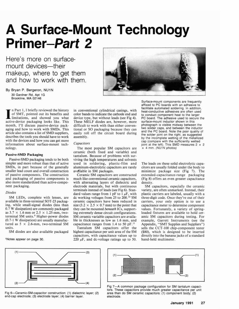
Surface-mount components are frequently affixed to PC boards with an adhesive to facilitate automated soldering. In addition, heat-conductive adhesives are often used to conduct component heat to the larger PC board. The adhesive used to secure the surface-mount inductor shown in this photograph is visible midway between the two solder caps, and between the inductor and the PC board. Note the poor quality of the solder joint on the right, as suggested by the incomplete wetting of the metallized cap (compare with the sufficiently wetted joint at the left). This SMD measures 2 x 2 x 4 mm. (NU1N photos)
The leads on these solid electrolytic capa- citors are usually folded under the body to minimize package size (Fig 7). The extended-capacitance-range packaging (Fig 8) offers an even greater capacitance density.
SM capacitors, especially the ceramic variety. are often unmarked. Instead, their plastic camers are labeled, usually with a three-digit code. Once they're out of their carriers, your only option is to use a capacitance meter to determine component values. Fortunately, a variety of spring- loaded fixtures are available to hold cer- amic SM capacitors during testing. For example, Garrett Instruments (see the Appendix, "SMT Supplies and Suppliers") sells the CCT-100 chip-component tester ($80). which is designed to be inserted directly into the banana jacks of a standard hand-held multimeter.
Fig 7-A common package configuration for SM tantalum capaci- tors. These capacitors provide much greater capacitance per unit
Fig &Ceramic-SMcapacitor construction: (1) dielectric layer; (2) area than do SM ceramic capacitors: (1) component body; (2) end-cap electrode; (3) electrode layer; (4) barrier layer. electrode.
January 1991 27

Fig &Extended SM tantalum capacitors provide the highest Fig 9--Metallized electrode face (MELF) resistor construction. capacitance per unit area, with values up to 220 pF available. (1) helix of resistive material; (2) end cap electrode; (3) protective Note that in this package configuration, the anode (+) is hidden lacquer coating; (4) ceramic core; (5) nickellchromium protective from view when mounted: (1) component body; (2) electrode. coating.
Resistors Most SM resistors are based on thick-
film technology, in which a resistor paste is fired over a ceramic base. A glass layer protects the device, and a film of plati- num/silver or platinum/palladium/silver forms the electrodes. A thin layer of barium is often applied over the electrodes to minimize leaching during the soldering process, and a tin coating is applied to pro- vide an easily solderable surface.
MELF resistors, adaptations of conven- tional leaded resistors in which metallized end electrodes are used instead of leads (see Fig 9), are also readily available. MELF resistors are somewhat less expensive than thick-film SM resistors. MELF devices are more difficult to work with, however. Like MELF diodes, they tend to roll off the PC board if not adequately secured with adhe- sive prior to soldering.
SM fined-resistor networks are attractive alternatives to individual SM thick-film resistors because they increase circuit den- sity and reduce mounting costs. There are two basic types of SM resistor-network packages (see Fig 10): the SO package with metal leads, and the leadless chip type.I2 Leadless SM resistor networks with con- cave electrodes are generally considered to be superior to the convex-electrode varie- ty because solder bridges are much less like-
ly to form during soldering. Also, the surface tension of the molten solder tends to self-align a network with concave elec- trodes to the underlying solder pad.
The labeling of individual SM fined resis- tors and SM networks departs from the familiar color bands used with conven- tional components. SM resistors are usually labeled with a three-digit code, in which 10-R, 1-kR, and 1-MR resistors are labeled 100, 102, and 105, respectively. That is, the first two digits correspond to the basic resis- tor value, and the third digit is the multipli- er (ie, 10 x 10" = 10, 10 x 102 = 1000, and 10 x 10S = 1,000,000).
Inductors Compact SM inductors are available in
values from 0.1 pH to 2.2 mH, with cur- rent ratings up to 0.5 A. Some 2.2-mH SM coils require minimum circuit-board real estate (4.5 x 3.2 x 2.6 mm). Completely shielded SM inductors (with values up to 220 pH) can mount in a space of only 3.2 x 2.5 x 1.1 mm.l3 SM inductors are usually constructed with a ceramic or fer- rite core that is coated with a protective epoxy resin.
Switches Despite their mechanical complexity, SM
toggle and push-button switches are easy to work with. For example, SM switches typically use gull-wing terminals, making their solder joints readily accessible for probing and visual inspection.I4 Because they must withstand molten solder, SM switches are constructed of heat-resistant resins.
Transformers SM transformers have been developed
that require less than 20% of the space of comparable conventional transformers. TDK Corporation offers a 5 x 6 x 3.1-mm SM transformer that includes a complete magnetic shield. The ferromag- netic shielding of this six-terminal device
Fig 10--SM resistor networks are available minimizes cross coupling, thereby support- in leaded (A) and more compact leadless ing very-high-density mounting configu- packages (B). Resistor-network value markings follow those of individual SM rations. resistors. For example, the networks pictured are both composed of four 1-kQ LC resistor units: 10 x lo2 = 1000 R. Several manufacturers offer ultraminia-
ture low-pass, band-pass, and high-pass SM filters. TDK Corporation manufactures a line of lightweight. 12-terminal, fully shielded LC filters with dimensions of only 3.6 x 5 x 2.3 mm.
Working with SMDs When laying out traces on an SMT cir-
cuit board, strive for a clean design that allows for adequate cooling and subsequent testing and repair.'$ Although the SM package type and lead tolerances dictate the number, thickness, and spacing of the required solder pads, you have great flexi- bility in defining the intercomponent space. Because surface-mount devices are so small, you can usually afford to be gener- ous with test points. By including dedicat-
Fig 11 -When designing SM circuit boards, make certain to allow for circuit probing. At A, an SM resistor (left) and transistor (right) are located immediately adjacent to each other. Although compact, this arrangement hinders testing. A better approach (B) is to extend solder pads well beyond component outlines. A second remedy is to design test points into the board layout (C). These test points should be located at least 1.2 mm (0.05 in.) from the nearest component.

ed test points in the circuit-board design, or simply extending solder pads beyond their component outlines (see Fig 11). cir- cuit testing is greatly simplified. Where working with SMDs does deviate signifi- cantly from working with conventional components is in component handling, sol- dering and testing.
Handling Components Although it's easy to accidentally bend
a lead on a 196-pin gull-wing QFP IC, SMDs in general are very rugged. Even so, tarnishing is a major problem with SMDs, and is a common cause of poor component solderability. Because sweat deposits, residue from coughing and sneezing, and other organic contaminants promote tar- nishing, never use your fingers to manipu- late an SMD: Use tweezers or a vacuum pencil. The tweezers should be angled, with a flat rather than pointed end, and should be used to grip the component across the body. Picking up an SMD by a metallized surface can cause irreparable damage to the device. Similarly, rather than using conven- tional test probes to verify component values, it is much safer to use specially designed microtip or tweezer probes.
Soldering Manufacturers rely on two soldering
methods when mounting SMDs: flow and reflow soldering. With flow soldering, a populated board is passed through molten solder. Adhesives are required to hold SMDs in place during the soldering process. Reflow soldering involves the deposition of solder paste on the circuit board pads, posi- tioning the SMDs on the board, and heat- ing the entire assembly to the soldering temperature. The differences between these two soldering techniques become relevant to amateurs when components must be removed from the board for repair (see Testing and Repair).
Although most SMDs are capable of withstanding temperatures of 500 OF for between 5 and 10 seconds, you should limit both soldering time and temperature as much as possible. The solder terminals on SM capacitors, resistors, and other leadless SMDs are usually composed of a mixture of glass and metallic flakes, commonly silver/palladium. Because these flakes are designed to be readily soluble in solder, they can be leached out of the component, leaving nonconductive glass behind. To retard leaching, components manufactured with silver/palladium metallizing should be soldered with the same metal: tin/lead/ silver solder should be used with silver/ palladium leads instead of tin/lead solder. With its lower melting point of 354 O F
(versus 370 OF for 60/40 tin/lead solder). tin/lead/silver solder is an excellent choice for all SMD soldering operations. Lower solder exposure time and temperatures minimize leaching.
With SMDs, don't use the conventional method of applying solder to the lead/ board junction while applying heat. Pre- tin the solder pads (see Fig 12). After the
Fig 12-Soldering leadless SM components is best accomplished by: (1) tinning the soldering pads with a low-temperature iron; (2) allowing the tinned pads to cool; (3) placing the component on the tinned pads and applying the tip of the iron to the solder pad, taking care to move the iron tip near, but never in direct contact with, the component terminal; (4) allowing the termi- nal to cool briefly before soldering the other terminal.
solder pads have been tinned, position the component over the pads (see Fig 13). (It is rarely necessary to apply adhesives, unless a thermally conductive adhesive is required for added heat dissipation.) Once the component has been positioned, place the iron tip on the pad and bring it near the component until the solder flows. Avoid bringing the iron tip into direct con- tact with the SMD body; position the iron at the junction of the PC-board foil and component solder terminals.
Take care to limit soldering time as much
Fig 13--Verifying proper alignment of SM components is important during both circuit testing and construction. For a highly reliable connection, no more than 25% of a component terminal should extend beyond its solder pad outline. (A)-an S M capacitor perfectly aligned with its solder pad outline. (B)-an SM capacitor with more than 50% of one terminal (the 50% mark is indicated by the dotted line) extending beyond its solder pad outline. This component should be remounted.
as possible when working with capacitors, resistors, and other components made of ceramic. Since these components conduct heat well, it's all too easy to unsolder one end of the device while attempting to solder the other. When working with transistors and ICs, tack down one pin, then quickly go through all of the pins in turn until the joints are bright. Don't use excessive amounts of solder.
When soldering leadless SMDs, the shape of the solder joint is a much better indicator of the quality of the connection than the texture or brightness of the joint. As illustrated in Fig 14, an adequate solder joint has a concave meniscus of solder that blends cleanly into the body of the com- ponent and the solder pad.
Testing and Repair Testing an SMD board is in some
respects easier than testing a conventional multilayer board. Because the traces and components are (for the most part) limited to one side of the circuit board, it can be much easier to follow circuit connections. This advantage, however, is often offset by the difficulty in working with the much finer traces and leads associated with SMDs.
When performing in-circuit testing of SMDs, don't probe component terminals directly. The pressure of the probe could momentarily make an open joint appear intact (or vice versa) and could also damage the component. If standard test leads are used, probe the nearest test pad or extended solder pad, if available. Alternatively, a microtip probe can be used to probe the edge of a standard solder pad. Specially designed tweezer probes can also be used to safely measure circuit parameters.
With conventional leaded components, removing a defective unit entails first removing any excess solder, and then free- ing the component. When removing SMDs, however, you must first reflow all of the solder connections, remove the device, then remove the excess solder. The most practi- cal method of removing SMDs involves the use of a temperature-controlled iron set at 500 OF and fitted with a tip just wide enough to bridge both ends of the compo- nent to be removed.I6 (Many of the tips sold for IC removal are good for remov- ing SMDs). Position the iron so that the tip makes good contact with both ends of the component, ensuring that maximum heat transfer takes place. When the solder melts, use tweezers to remove the component. If an adhesive was used in production, a slight twisting of the component usually frees it from the PC board. After the board has cooled for a few minutes, remove the excess solder with desoldering braid.
Angled side cutters can also be used to remove suspect SM components. However, not only does this method render the com- ponent useless, but the PC board may also be damaged in the process.
Once a defective SMD has been removed and the excess solder removed from the PC board, replacing the component is straight-
January 1991 29

Fig 14-The optimum size, shape and extent of the PCboard SMD solder fillets depend on the device and lead type. The solder joint of a leadless SMD should have a concave meniscus of solder that blends cleanly into the body of the component and the solder pad (right). In addition, the solder fillet must wet at least 50% of the face of the SMD terminal, and extend up the face of the component terminal by at least 0.5 mm (0.020 in.) or 25% of the terminal height, whichever is less. The solder joint on the left is inadequate. In high-reliability applications, no more than 25% of the terminal should extend beyond the pad.
forward. As described earlier, position the replacement component and place the iron tip on the component pad, bringing it nearer t o the component until the solder flows.
SMT OntIook The advantages of SMT, including
reduced equipment size, low-profile design and reduced mounting costs, promise to make it the dominant component technol- ogy throughout the next decade. Use of the once-popular plastic DIP has decreased precipitously in the last few years, having been supplanted by new SM packaging alternatives." With traditional compo- nents going the way of the once ubiquitous vacuum tube, radio amateurs should learn t o work with SMT.
Pick up a few SM capacitors and resis- tors, and work them into your next project design. After you feel comfortable handling these robust and relatively inex- pensive devices, you can move up t o more challenging work with SM transistors, diodes, and ICs.
APPENDIX SMT Supplies and Soppliers
The basic supplies required for SMD work are tweezers, a low- or temperature-controlled soldering iron with a fine tip for mounting components and a wider or specialized tip for removing them, and a vision aid. If you don't have a desk- or bench-mounted magnifier lamp, you'll need some sort of hand-held magnifier to inspect solder joints and deter- mine component values. Listed below are but a few of the many vendors of SMDs and ac- cessories.
SMDs Communications Specialists, Inc (426
West Taft Ave. Orange. CA 92665. tel 800-854-0547) offers SM chip prototyping kits. A 365-piece SM capacitor sampler, with values from 1 pF to 0.33 pF (most are rated at 50 V dc), sells for $49.95. For the same price, you can purchase a 1540-piece resistor sampler, with values from 10 Q to 10 MQ (1/10 to 1/8 W).
Garrett IEU, Inc (3130 Skyway Dr. #104, Santa Maria CA 93455, tel 805-922-0594) is an excellent source of virtually all SMDs. from Fied and variable resistors and capaci- tors (tantalum units up to 220 pF), to inductors, transistors and ICs. Their exten- sive 51-page catalog, which is free for the asking, contains detailed data sheets on many components. The numerous illustrations, in- cluding suggested pad layouts, device outlines and component details, such as temperature characteristics, maximum operating voltage, etc, make this catalog a valuable reference for anyone working with SMT.
MCM Electronics (650 Congress Park Dr, Centerville, OH 454594072. tel800-5434330) offers SM capacitors and resistors in bags of 10. Prices for a bag of capacitors range from $1.30 to $2.35, with values available from 10 pF to 0.1 pF at 50 V dc. A bag of ten 5%-tolerance, 1/8-W resistors, with values from 20 Q to 750 kQ, sells for $0.65.
ROHM Corporation (8 Whatney. Irvine, CA 97218, tel 714-855-2131) offers a full range of SMDs, including monolithic and hybrid ICs, transistors, diodes (switching. Zener, laser. Schottky, light emitting, and variable capacitance), foced and variable resis- tors, ceramic capacitors and LCDs.
Radio Shackm has introduced a 200-piece assortment of 1 4 - W surface-mount resistors (RS 271-3 13).
Tools In addition to SMDs, MCM Electronics
markets an inexpensive tweezer/magnifying lens combination designed expressly for work- ing with SMDs ($3.95). as well as a low-cost magnifier attachment for a helping-hands station ($1.95). Similarly. Garrett IEU, Inc, markets a complete line of ITT Pomona test equipment, including SMD test tweezers ($17.60). an SMD microtip test probe ($8.20). and dozens of other SMD test probes and clips.
Edmund Scientific Co (101 E Gloucester Pike. Barrinaton. NJ 08007-1380. tel 609-573-6260) markets a complete line of highquality magnifiers, pocket microscopes, and other visual aids that can be used for SM work. In particular, they offer a hands- free magnifier by Bausch & Lomb that is secured around the neck and rests against the chest, leaving both hands free for soldering
and probing ($20). Fordham Radio (260 Motor Parkway.
Hauppauge, NY 11788-5 134. tel 800-832-1446) sells a wide variety of precision electronic assembly tweezers ($8 and up), as well as an X-ACT@' x-tra hands station with magnifier ($19.95).
Jamecoa Electronics (1355 Shoreway Rd, Belmont. CA 94002. tel 415-592-8097) sells an assortment of soldering stations and soldering accessories.
Jensen Tools, Inc (7815 S 46th Street, Phoenix. AZ 85044-5399. tel 602-968-6231) offers the most impressive array of precision tweezers that I have seen (carbon, stainless steel, and titanium units, from Swiss manufacturers). In addition, a vacuum part- handling system, perfect for working with SMDs, is available for about $50. Jensen also handles the complete line of Wellere and Ungarm soldering stations, as well as KesteP 60/40 and 63/37 tin-lead solders and 62/36/2 tin-lead-silver solder.
Books Heath Co. (PO Box 8589, Benton Harbor,
MI 49022, tel800-253-0570) markets a home study course on SMT for about $100. Along with a fairly comprehensive manual, the course contains PC boards designed for SMDs and the components required to popu- late them. This course provides a gentle introduction to the practical aspects of work- ing with SMDs. An alternative to this course is to equip yourself with a good set of tweez- ers, a magnifying glass, some PC-board stock, a few dozen assorted SMDs and the catalog from Garrett. In addition to the course from Heath, a number of excellent texts on SMT are available (some of which are identified under Notes). Consult your local library for these and other SMT references.
Notes 9T. Okada, "Chip Components Open Door Wide
to Greater Mounting Densities." Joumalof Elec- tronic Engineering, Oct 1989, pp 102-105.
1oH. Manko, Soldering Handbook for Printed Circuits andsutface Mwntmg, (New York: Van Nostrand Company. Inc 1986).
1lY. Higuchi. "Overcoming Technical Hurdles on the Road to SMT and Miniaturization." Journal of EIectroni~~Engineering~Oct 1989, pp 1W109.
(2s. Inagaki. Chlp Reststor Network Reduces Mountings on the Way to Higher Density Cir- cuits," Journal of Electronic Engineermg. Oct 1989, pp 119-121.
1W. Takaya. "Surface Mounting Technologies for Chin Transformers. Filters and Inductors." ~ o u h a l of ~lectronic Engineering. Oct 1989, pp 116-118.
1sT. Nakamura. "New Technology Emerges for Surface-Mount Toggle Switches." Journal of Electronic Engineering, Oct 1989. pp 1 14-1 15.
1The 1986-1990 editions of The ARRL Handbook featured "A Computer Controlled Shortwave Converter." (pp 30-25 to 3040). This project, built by Lee Snook, WlDN, makes extensive use of surface-mount technology.
1eAlthough vacuumdesoldering machines, heated tweezers, hot-gas pencils, hot-air machines, focused infrared energy, heat guns, and hot- bar soldering are used commerc~ally to remove SMDs, these approaches are far too expensive for the average amateur.
'7J. Scarlett, An Introduction to Printed Circuit Board Technology, (Ayr, Scotland: Electro- chemical Publlcatlons Ltd. 1984). 'm