A SUBSTRATE INTEGRATED WAVEGUIDE BANDPASS FILTER …A SUBSTRATE INTEGRATED WAVEGUIDE BANDPASS FILTER...
13
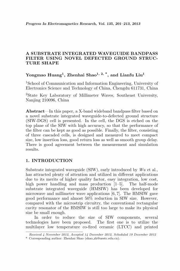
Progress In Electromagnetics Research, Vol. 135, 201–213, 2013 A SUBSTRATE INTEGRATED WAVEGUIDE BANDPASS FILTER USING NOVEL DEFECTED GROUND STRUC- TURE SHAPE Yongmao Huang 1 , Zhenhai Shao 1, 2, * , and Lianfu Liu 1 1 School of Communication and Information Engineering, University of Electronics Science and Technology of China, Chengdu 611731, China 2 State Key Laboratory of Millimeter Waves, Southeast University, Nanjing 210096, China Abstract—In this paper, a X-band wideband bandpass filter based on a novel substrate integrated waveguide-to-defected ground structure (SIW-DGS) cell is presented. In the cell, the DGS is etched on the top plane of the SIW with high accuracy, so that the performance of the filter can be kept as good as possible. Finally, the filter, consisting of three cascaded cells, is designed and measured to meet compact size, low insertion loss, good return loss as well as smooth group delay. There is good agreement between the measurement and simulation results. 1. INTRODUCTION Substrate integrated waveguide (SIW), early introduced by Wu et al., has attracted plenty of attention and utilized in different applications due to its merits of higher quality factor, easy integration, low cost, high power handling and mass production [1–5]. The half-mode substrate integrated waveguide (HMSIW) has been developed for microwave and millimeter wave applications [6,7]. The HMSIW gave good performance and almost 50% reduction in SIW size. However, compared with the microstrip circuitry, the conventional rectangular cavity resonator of the HMSIW is still too large to make its physical size be small enough. In order to reduce the size of SIW components, several technologies have been proposed. The first one is to utilize the multilayer low temperature co-fired ceramic (LTCC) and printed Received 4 November 2012, Accepted 14 December 2012, Scheduled 19 December 2012 * Corresponding author: Zhenhai Shao (shao [email protected]).
Transcript of A SUBSTRATE INTEGRATED WAVEGUIDE BANDPASS FILTER …A SUBSTRATE INTEGRATED WAVEGUIDE BANDPASS FILTER...
Progress In Electromagnetics Research, Vol. 135, 201–213, 2013
A SUBSTRATE INTEGRATED WAVEGUIDE BANDPASSFILTER USING NOVEL DEFECTED GROUND STRUC-TURE SHAPE
Yongmao Huang1, Zhenhai Shao1, 2, *, and Lianfu Liu1
1School of Communication and Information Engineering, University ofElectronics Science and Technology of China, Chengdu 611731, China2State Key Laboratory of Millimeter Waves, Southeast University,Nanjing 210096, China
Abstract—In this paper, a X-band wideband bandpass filter based ona novel substrate integrated waveguide-to-defected ground structure(SIW-DGS) cell is presented. In the cell, the DGS is etched on thetop plane of the SIW with high accuracy, so that the performance ofthe filter can be kept as good as possible. Finally, the filter, consistingof three cascaded cells, is designed and measured to meet compactsize, low insertion loss, good return loss as well as smooth group delay.There is good agreement between the measurement and simulationresults.
1. INTRODUCTION
Substrate integrated waveguide (SIW), early introduced by Wu et al.,has attracted plenty of attention and utilized in different applicationsdue to its merits of higher quality factor, easy integration, low cost,high power handling and mass production [1–5]. The half-modesubstrate integrated waveguide (HMSIW) has been developed formicrowave and millimeter wave applications [6, 7]. The HMSIW gavegood performance and almost 50% reduction in SIW size. However,compared with the microstrip circuitry, the conventional rectangularcavity resonator of the HMSIW is still too large to make its physicalsize be small enough.
In order to reduce the size of SIW components, severaltechnologies have been proposed. The first one is to utilize themultilayer low temperature co-fired ceramic (LTCC) and printed
Received 4 November 2012, Accepted 14 December 2012, Scheduled 19 December 2012* Corresponding author: Zhenhai Shao (shao [email protected]).
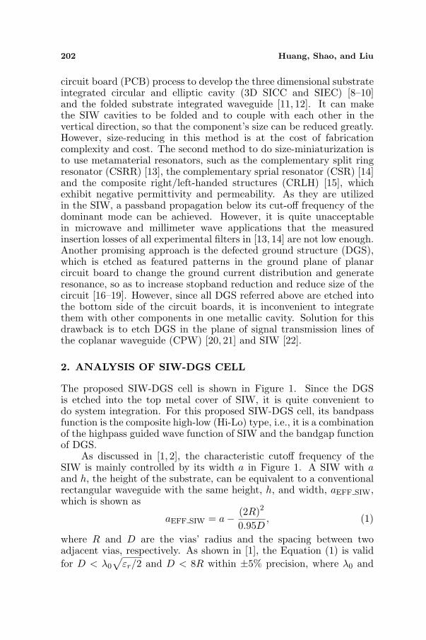
202 Huang, Shao, and Liu
circuit board (PCB) process to develop the three dimensional substrateintegrated circular and elliptic cavity (3D SICC and SIEC) [8–10]and the folded substrate integrated waveguide [11, 12]. It can makethe SIW cavities to be folded and to couple with each other in thevertical direction, so that the component’s size can be reduced greatly.However, size-reducing in this method is at the cost of fabricationcomplexity and cost. The second method to do size-miniaturization isto use metamaterial resonators, such as the complementary split ringresonator (CSRR) [13], the complementary sprial resonator (CSR) [14]and the composite right/left-handed structures (CRLH) [15], whichexhibit negative permittivity and permeability. As they are utilizedin the SIW, a passband propagation below its cut-off frequency of thedominant mode can be achieved. However, it is quite unacceptablein microwave and millimeter wave applications that the measuredinsertion losses of all experimental filters in [13, 14] are not low enough.Another promising approach is the defected ground structure (DGS),which is etched as featured patterns in the ground plane of planarcircuit board to change the ground current distribution and generateresonance, so as to increase stopband reduction and reduce size of thecircuit [16–19]. However, since all DGS referred above are etched intothe bottom side of the circuit boards, it is inconvenient to integratethem with other components in one metallic cavity. Solution for thisdrawback is to etch DGS in the plane of signal transmission lines ofthe coplanar waveguide (CPW) [20, 21] and SIW [22].
2. ANALYSIS OF SIW-DGS CELL
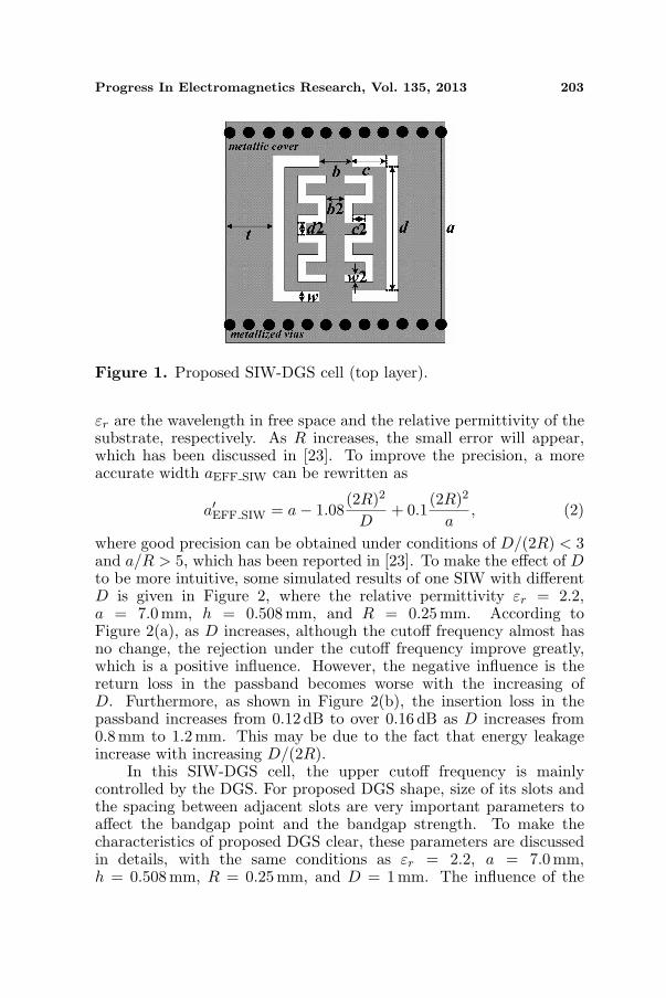
The proposed SIW-DGS cell is shown in Figure 1. Since the DGSis etched into the top metal cover of SIW, it is quite convenient todo system integration. For this proposed SIW-DGS cell, its bandpassfunction is the composite high-low (Hi-Lo) type, i.e., it is a combinationof the highpass guided wave function of SIW and the bandgap functionof DGS.
As discussed in [1, 2], the characteristic cutoff frequency of theSIW is mainly controlled by its width a in Figure 1. A SIW with aand h, the height of the substrate, can be equivalent to a conventionalrectangular waveguide with the same height, h, and width, aEFF SIW,which is shown as
aEFF SIW = a− (2R)2
0.95D, (1)
where R and D are the vias’ radius and the spacing between twoadjacent vias, respectively. As shown in [1], the Equation (1) is validfor D < λ0
√εr/2 and D < 8R within ±5% precision, where λ0 and
Progress In Electromagnetics Research, Vol. 135, 2013 203
Figure 1. Proposed SIW-DGS cell (top layer).
εr are the wavelength in free space and the relative permittivity of thesubstrate, respectively. As R increases, the small error will appear,which has been discussed in [23]. To improve the precision, a moreaccurate width aEFF SIW can be rewritten as
a′EFF SIW = a− 1.08(2R)2
D+ 0.1
(2R)2
a, (2)
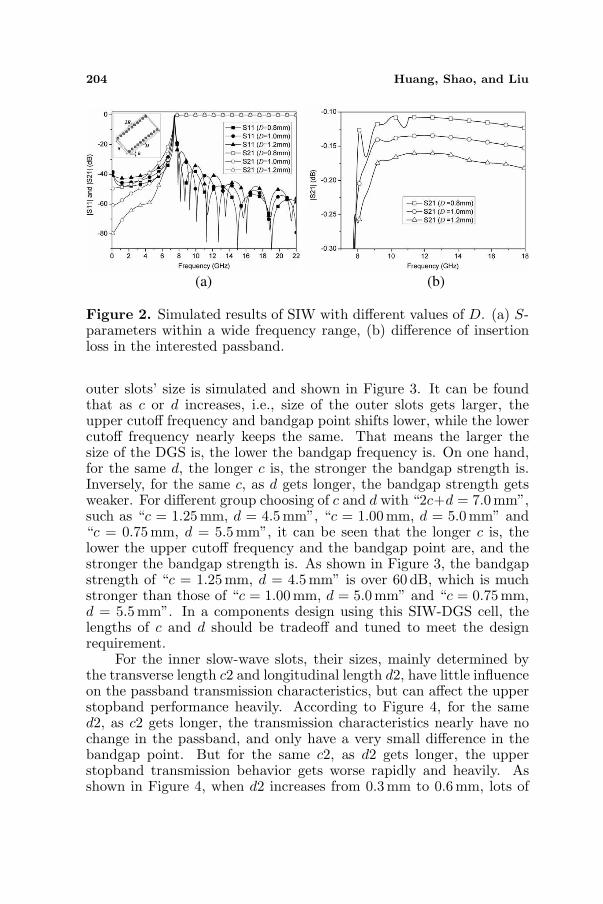
where good precision can be obtained under conditions of D/(2R) < 3and a/R > 5, which has been reported in [23]. To make the effect of Dto be more intuitive, some simulated results of one SIW with differentD is given in Figure 2, where the relative permittivity εr = 2.2,a = 7.0 mm, h = 0.508mm, and R = 0.25 mm. According toFigure 2(a), as D increases, although the cutoff frequency almost hasno change, the rejection under the cutoff frequency improve greatly,which is a positive influence. However, the negative influence is thereturn loss in the passband becomes worse with the increasing ofD. Furthermore, as shown in Figure 2(b), the insertion loss in thepassband increases from 0.12 dB to over 0.16 dB as D increases from0.8mm to 1.2mm. This may be due to the fact that energy leakageincrease with increasing D/(2R).
In this SIW-DGS cell, the upper cutoff frequency is mainlycontrolled by the DGS. For proposed DGS shape, size of its slots andthe spacing between adjacent slots are very important parameters toaffect the bandgap point and the bandgap strength. To make thecharacteristics of proposed DGS clear, these parameters are discussedin details, with the same conditions as εr = 2.2, a = 7.0mm,h = 0.508 mm, R = 0.25 mm, and D = 1 mm. The influence of the
204 Huang, Shao, and Liu
(a) (b)
Figure 2. Simulated results of SIW with different values of D. (a) S-parameters within a wide frequency range, (b) difference of insertionloss in the interested passband.
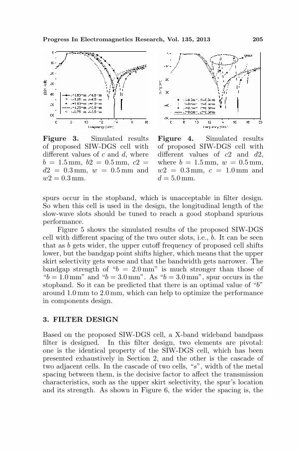
outer slots’ size is simulated and shown in Figure 3. It can be foundthat as c or d increases, i.e., size of the outer slots gets larger, theupper cutoff frequency and bandgap point shifts lower, while the lowercutoff frequency nearly keeps the same. That means the larger thesize of the DGS is, the lower the bandgap frequency is. On one hand,for the same d, the longer c is, the stronger the bandgap strength is.Inversely, for the same c, as d gets longer, the bandgap strength getsweaker. For different group choosing of c and d with “2c+d = 7.0mm”,such as “c = 1.25mm, d = 4.5mm”, “c = 1.00mm, d = 5.0mm” and“c = 0.75mm, d = 5.5mm”, it can be seen that the longer c is, thelower the upper cutoff frequency and the bandgap point are, and thestronger the bandgap strength is. As shown in Figure 3, the bandgapstrength of “c = 1.25mm, d = 4.5mm” is over 60 dB, which is muchstronger than those of “c = 1.00mm, d = 5.0mm” and “c = 0.75mm,d = 5.5mm”. In a components design using this SIW-DGS cell, thelengths of c and d should be tradeoff and tuned to meet the designrequirement.
For the inner slow-wave slots, their sizes, mainly determined bythe transverse length c2 and longitudinal length d2, have little influenceon the passband transmission characteristics, but can affect the upperstopband performance heavily. According to Figure 4, for the samed2, as c2 gets longer, the transmission characteristics nearly have nochange in the passband, and only have a very small difference in thebandgap point. But for the same c2, as d2 gets longer, the upperstopband transmission behavior gets worse rapidly and heavily. Asshown in Figure 4, when d2 increases from 0.3 mm to 0.6 mm, lots of
Progress In Electromagnetics Research, Vol. 135, 2013 205
Figure 3. Simulated resultsof proposed SIW-DGS cell withdifferent values of c and d, whereb = 1.5mm, b2 = 0.5mm, c2 =d2 = 0.3mm, w = 0.5mm andw2 = 0.3 mm.
Figure 4. Simulated resultsof proposed SIW-DGS cell withdifferent values of c2 and d2,where b = 1.5 mm, w = 0.5mm,w2 = 0.3mm, c = 1.0 mm andd = 5.0mm.
spurs occur in the stopband, which is unacceptable in filter design.So when this cell is used in the design, the longitudinal length of theslow-wave slots should be tuned to reach a good stopband spuriousperformance.
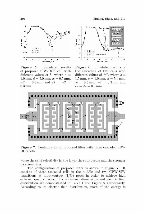
Figure 5 shows the simulated results of the proposed SIW-DGScell with different spacing of the two outer slots, i.e., b. It can be seenthat as b gets wider, the upper cutoff frequency of proposed cell shiftslower, but the bandgap point shifts higher, which means that the upperskirt selectivity gets worse and that the bandwidth gets narrower. Thebandgap strength of “b = 2.0 mm” is much stronger than those of“b = 1.0mm” and “b = 3.0mm”. As “b = 3.0mm”, spur occurs in thestopband. So it can be predicted that there is an optimal value of “b”around 1.0 mm to 2.0 mm, which can help to optimize the performancein components design.
3. FILTER DESIGN
Based on the proposed SIW-DGS cell, a X-band wideband bandpassfilter is designed. In this filter design, two elements are pivotal:one is the identical property of the SIW-DGS cell, which has beenpresented exhaustively in Section 2, and the other is the cascade oftwo adjacent cells. In the cascade of two cells, “s”, width of the metalspacing between them, is the decisive factor to affect the transmissioncharacteristics, such as the upper skirt selectivity, the spur’s locationand its strength. As shown in Figure 6, the wider the spacing is, the
206 Huang, Shao, and Liu
Figure 5. Simulated resultsof proposed SIW-DGS cell withdifferent values of b, where c =1.0mm, d = 5.0mm, w = 0.5mm,w2 = 0.3mm and c2 = d2 =0.3mm.
Figure 6. Simulated results ofthe cascading of two cells withdifferent values of “s”, where b =1.5mm, c = 1.0mm, d = 5.0mm,w = 0.5 mm, w2 = 0.3 mm andc2 = d2 = 0.3mm.
Figure 7. Configuration of proposed filter with three cascaded SIW-DGS cells.
worse the skirt selectivity is, the lower the spur occurs and the strongerits strength is.
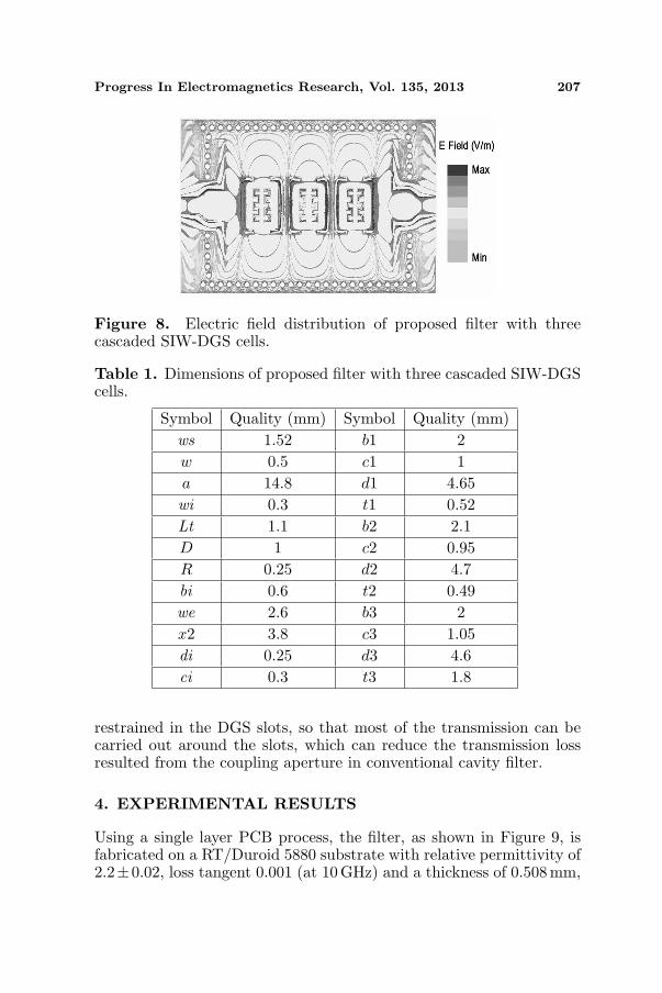
The configuration of proposed filter is shown in Figure 7. Itconsists of three cascaded cells in the middle and two CPW-SIWtransitions at input/output (I/O) ports in order to achieve highexternal quality factor. Its optimized dimensions and electric fielddistribution are demonstrated in Table 1 and Figure 8, respectively.According to its electric field distribution, most of the energy is
Progress In Electromagnetics Research, Vol. 135, 2013 207
Figure 8. Electric field distribution of proposed filter with threecascaded SIW-DGS cells.
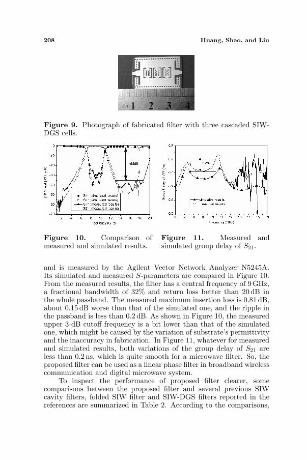
Table 1. Dimensions of proposed filter with three cascaded SIW-DGScells.
Symbol Quality (mm) Symbol Quality (mm)ws 1.52 b1 2w 0.5 c1 1a 14.8 d1 4.65wi 0.3 t1 0.52Lt 1.1 b2 2.1D 1 c2 0.95R 0.25 d2 4.7bi 0.6 t2 0.49we 2.6 b3 2x2 3.8 c3 1.05di 0.25 d3 4.6ci 0.3 t3 1.8
restrained in the DGS slots, so that most of the transmission can becarried out around the slots, which can reduce the transmission lossresulted from the coupling aperture in conventional cavity filter.
4. EXPERIMENTAL RESULTS
Using a single layer PCB process, the filter, as shown in Figure 9, isfabricated on a RT/Duroid 5880 substrate with relative permittivity of2.2±0.02, loss tangent 0.001 (at 10GHz) and a thickness of 0.508 mm,
208 Huang, Shao, and Liu
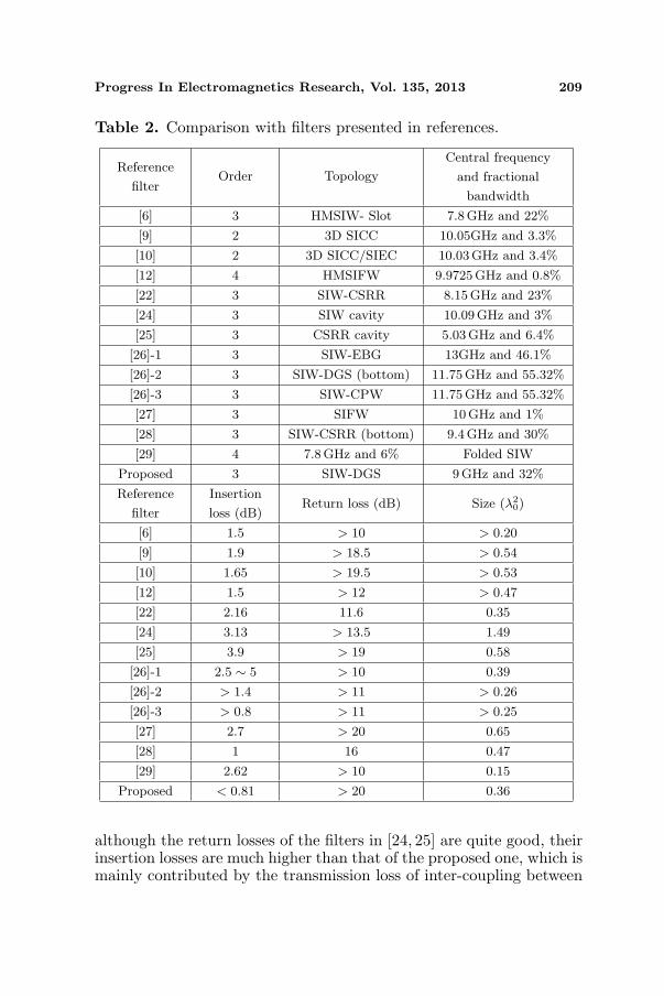
Figure 9. Photograph of fabricated filter with three cascaded SIW-DGS cells.
Figure 10. Comparison ofmeasured and simulated results.
Figure 11. Measured andsimulated group delay of S21.
and is measured by the Agilent Vector Network Analyzer N5245A.Its simulated and measured S-parameters are compared in Figure 10.From the measured results, the filter has a central frequency of 9 GHz,a fractional bandwidth of 32% and return loss better than 20 dB inthe whole passband. The measured maximum insertion loss is 0.81 dB,about 0.15 dB worse than that of the simulated one, and the ripple inthe passband is less than 0.2 dB. As shown in Figure 10, the measuredupper 3-dB cutoff frequency is a bit lower than that of the simulatedone, which might be caused by the variation of substrate’s permittivityand the inaccuracy in fabrication. In Figure 11, whatever for measuredand simulated results, both variations of the group delay of S21 areless than 0.2 ns, which is quite smooth for a microwave filter. So, theproposed filter can be used as a linear phase filter in broadband wirelesscommunication and digital microwave system.
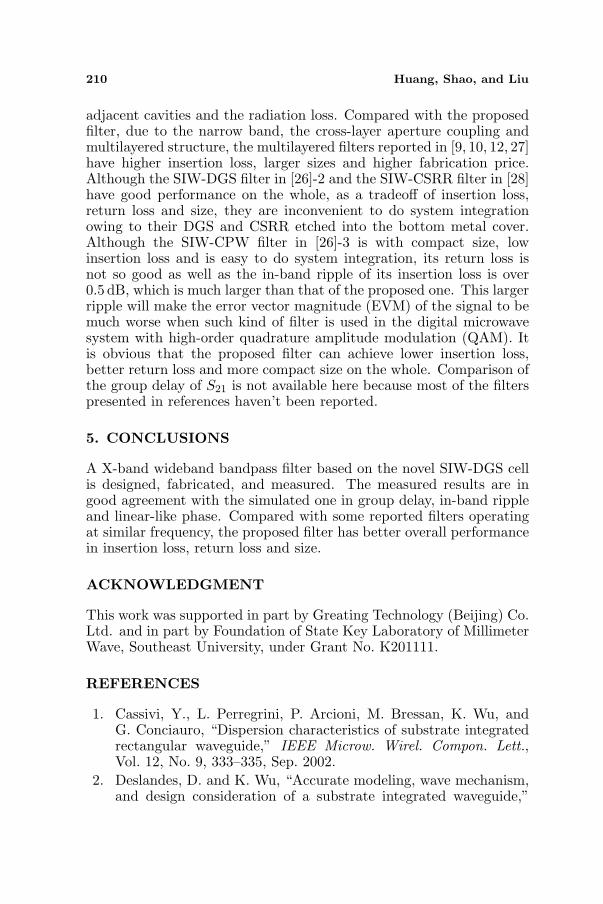
To inspect the performance of proposed filter clearer, somecomparisons between the proposed filter and several previous SIWcavity filters, folded SIW filter and SIW-DGS filters reported in thereferences are summarized in Table 2. According to the comparisons,
Progress In Electromagnetics Research, Vol. 135, 2013 209
Table 2. Comparison with filters presented in references.
Reference
filterOrder Topology
Central frequency
and fractional
bandwidth
[6] 3 HMSIW- Slot 7.8GHz and 22%
[9] 2 3D SICC 10.05GHz and 3.3%
[10] 2 3D SICC/SIEC 10.03 GHz and 3.4%
[12] 4 HMSIFW 9.9725GHz and 0.8%
[22] 3 SIW-CSRR 8.15GHz and 23%
[24] 3 SIW cavity 10.09GHz and 3%
[25] 3 CSRR cavity 5.03GHz and 6.4%
[26]-1 3 SIW-EBG 13GHz and 46.1%
[26]-2 3 SIW-DGS (bottom) 11.75GHz and 55.32%
[26]-3 3 SIW-CPW 11.75GHz and 55.32%
[27] 3 SIFW 10GHz and 1%
[28] 3 SIW-CSRR (bottom) 9.4GHz and 30%
[29] 4 7.8GHz and 6% Folded SIW
Proposed 3 SIW-DGS 9GHz and 32%
Reference
filter
Insertion
loss (dB)Return loss (dB) Size (λ2
0)
[6] 1.5 > 10 > 0.20
[9] 1.9 > 18.5 > 0.54
[10] 1.65 > 19.5 > 0.53
[12] 1.5 > 12 > 0.47
[22] 2.16 11.6 0.35
[24] 3.13 > 13.5 1.49
[25] 3.9 > 19 0.58
[26]-1 2.5 ∼ 5 > 10 0.39
[26]-2 > 1.4 > 11 > 0.26
[26]-3 > 0.8 > 11 > 0.25
[27] 2.7 > 20 0.65
[28] 1 16 0.47
[29] 2.62 > 10 0.15
Proposed < 0.81 > 20 0.36
although the return losses of the filters in [24, 25] are quite good, theirinsertion losses are much higher than that of the proposed one, which ismainly contributed by the transmission loss of inter-coupling between
210 Huang, Shao, and Liu
adjacent cavities and the radiation loss. Compared with the proposedfilter, due to the narrow band, the cross-layer aperture coupling andmultilayered structure, the multilayered filters reported in [9, 10, 12, 27]have higher insertion loss, larger sizes and higher fabrication price.Although the SIW-DGS filter in [26]-2 and the SIW-CSRR filter in [28]have good performance on the whole, as a tradeoff of insertion loss,return loss and size, they are inconvenient to do system integrationowing to their DGS and CSRR etched into the bottom metal cover.Although the SIW-CPW filter in [26]-3 is with compact size, lowinsertion loss and is easy to do system integration, its return loss isnot so good as well as the in-band ripple of its insertion loss is over0.5 dB, which is much larger than that of the proposed one. This largerripple will make the error vector magnitude (EVM) of the signal to bemuch worse when such kind of filter is used in the digital microwavesystem with high-order quadrature amplitude modulation (QAM). Itis obvious that the proposed filter can achieve lower insertion loss,better return loss and more compact size on the whole. Comparison ofthe group delay of S21 is not available here because most of the filterspresented in references haven’t been reported.
5. CONCLUSIONS
A X-band wideband bandpass filter based on the novel SIW-DGS cellis designed, fabricated, and measured. The measured results are ingood agreement with the simulated one in group delay, in-band rippleand linear-like phase. Compared with some reported filters operatingat similar frequency, the proposed filter has better overall performancein insertion loss, return loss and size.
ACKNOWLEDGMENT
This work was supported in part by Greating Technology (Beijing) Co.Ltd. and in part by Foundation of State Key Laboratory of MillimeterWave, Southeast University, under Grant No. K201111.
REFERENCES
1. Cassivi, Y., L. Perregrini, P. Arcioni, M. Bressan, K. Wu, andG. Conciauro, “Dispersion characteristics of substrate integratedrectangular waveguide,” IEEE Microw. Wirel. Compon. Lett.,Vol. 12, No. 9, 333–335, Sep. 2002.
2. Deslandes, D. and K. Wu, “Accurate modeling, wave mechanism,and design consideration of a substrate integrated waveguide,”
Progress In Electromagnetics Research, Vol. 135, 2013 211
IEEE Trans. on Microw. Theory and Tech., Vol. 54, No. 6, 2516–2526, Jun. 2006.
3. Djerafi, T., N. J. G. Fonseca, and K. Wu, “Design andimplementation of a planar 4 × 4 Butler Matrix in SIWtechnology for wide band high power applications,” Progress InElectromagnetics Research B, Vol. 35, 29–51, 2011.
4. Cheng, Y. J., “Substrate integrated waveguide frequency-agileslot antenna and its multibeam application,” Progress InElectromagnetics Research, Vol. 130, 153–168, 2012.
5. Su, P., Z.-X. Tang, and B. Zhang, “Push-push dielectric resonatoroscillator using substrate integrated waveguide power combiner,”Progress In Electromagnetics Research Letters, Vol. 30, 105–113,2012.
6. Wang, Y. Q., W. Hong, Y. D. Dong, B. Liu, H. J. Tang,J. X. Chen, X. X. Yin, and K. Wu, “Half mode substrateintegrated waveguide (HMSIW) bandpass filter,” IEEE Microw.Wirel. Compon. Lett., Vol. 17, No. 4, 265–267, Apr. 2007.
7. Song, Q. Y., H. R. Cheng, X. H. Wang, L. Xu, X. Q. Chen, andX. W. Shi, “Novel wideband bandpass filter integrating HMSIWand DGS,” Journal of Electromagnetic Waves and Applications,Vol. 23, Nos. 14–15, 2031–2040, 2009.
8. Gu, J., Y. Fan, and Y. Zhang, “A X-band 3-D SICC filter withlow-loss and narrow band using LTCC technology,” Journal ofElectromagnetic Waves and Applications, Vol. 23, Nos. 8–9, 1093–1100, 2009.
9. Zhang, Z. G., Y. Fan, Y. J. Cheng, and Y.-H. Zhang, “A compactmultilayer dual-mode substrate integrated circular cavity (SICC)filter for X-band application,” Progress In ElectromagneticsResearch, Vol. 122, 453–465, 2012.
10. Zhang, Z. G., Y. Fan, Y. J. Cheng, and Y.-H. Zhang,“A novel multilayer dual-mode substrate integrated waveguidecomplementary filter with circular and elliptic cavities (SICC andSIEC),” Progress In Electromagnetics Research, Vol. 127, 173–188,2012.
11. Wang, R., L.-S. Wu, and X.-L. Zhou, “Compact folded substrateintegrated waveguide cavities and bandpass filter,” Progress InElectromagnetics Research, Vol. 84, 135–147, 2008.
12. Wang, Z., X. Li, S. Zhou, B. Yan, R.-M. Xu, and W. Lin,“Half mode substrate integrated folded waveguide (HMSIFW)and partial H-plane bandpass filter,” Progress In ElectromagneticsResearch, Vol. 101, 203–216, 2010.
212 Huang, Shao, and Liu
13. Dong, Y.-D., T. Yang, and T. Itoh, “Substrate integratedwaveguide loaded by complementary split-ring resonators and itsapplications to miniaturized waveguide filters,” IEEE Trans. onMicrow. Theory and Tech., Vol. 57, No. 9, 2211–2223, Sep. 2009.
14. Zhou, L., S. Liu, N. Gao, Y. Chen, and Y. Wei, “Miniaturizedsubstrate integrated waveguide filter with complementary sprialresonator,” Microwave and Optical Technology Letters, Vol. 53,No. 6, 1308–1311, Jun. 2011.
15. Dong, Y.-D. and T. Itoh, “Composite right/left-handed substrateintegrated waveguide and half-mode substrate integrated waveg-uide,” Proc. IEEE MTT-S International Microwave SymposiumDigest, 49–52, Jun. 2009.
16. Ahn, D., J.-S. Park, C.-S. Kim, J. Kim, Y.-X. Qian, and T. Itoh,“A design of the low-pass filter using the novel microstrip defectedground structure,” IEEE Trans. on Microw. Theory and Tech.,Vol. 49, No. 1, 86–93, Jan. 2001.
17. Chen, J., Z.-B. Weng, Y.-C. Jiao, and F.-S. Zhang, “Lowpass filterdesign of Hilbert curve ring defected ground structure,” ProgressIn Electromagnetics Research, Vol. 70, 269–280, 2007.
18. Sheta, A. F., “A novel compact degenerate dual-mode squarepatch filter using cross H-shaped defected ground structure,”Journal of Electromagnetic Waves and Applications, Vol. 22,Nos. 14–15, 1913–1923, 2008.
19. Gupta, N., P. Ghosh, and M. Toppo, “A miniaturized Wilkinsonpower divider using DGS and fractal structure for GSMapplication,” Progress In Electromagnetics Research Letters,Vol. 27, 25–31, 2011.
20. Shao, Z. H. and M. Fujise, “Bandpass filter design based on LTCCand DGS,” 17th Asia-Pacific Microwave Conference, 138–139,2005.
21. Ke, P.-Y., H.-C. Chiu, F.-H. Huang, H.-L. Kao, and Q. Xue,“Characterization of compact V-band GaAs CMRC filter usingslow wave CPW transmission lines technology,” Progress InElectromagnetics Research B, Vol. 43, 355–372, 2012.
22. Zhang, X.-C., Z.-Y. Yu, and J. Xu, “Novel band-pass substrateintegrated waveguide (SIW) filter based on complementary splitring resonators (CSRR),” Progress In Electromagnetics Research,Vol. 72, 39–46, 2007.
23. Xu, F. and K. Wu, “Guided-wave and leakage characteristics ofsubstrate integrated waveguide,” IEEE Trans. on Microw. Theoryand Tech., Vol. 53, No. 1, 66–73, Jan. 2005.
Progress In Electromagnetics Research, Vol. 135, 2013 213
24. Ismail, A., M. S. Razalli, M. A. Mahdi, R. S. A. R. Abdullah,N. K. Noordin, and M. F. A. Rasid, “X-band trisectionsubstrate-integrated waveguide quasi-elliptic filter,” Progress InElectromagnetics Research, Vol. 85, 133–145, 2008.
25. Jiang, W., W. Shen, L. Zhou, and W.-Y. Yin, “Miniaturized andhigh-selectivity substrate integrated waveguide (SIW) bandpassfilter loaded by complementary split-ring resonators (CSRRs),”Journal of Electromagnetic Waves and Applications, Vol. 26,Nos. 11–12, 1448–1459, Aug. 2010.
26. Hao, Z.-C., W. Hong, J.-X. Chen, X.-P. Chen, and K. Wu,“Compact super-wide bandpass substrate integrated waveguide(SIW) filters,” IEEE Trans. on Microw. Theory and Tech., Vol. 53,No. 9, 2968–2977, Sep. 2005.
27. Wang, Z., D. Shen, R. Xu, B. Yan, and W. Lin, “A partialH-plane substrate integrated folded waveguide (SIFW) bandpassfilter based on H-plane slot,” Journal of Electromagnetic Wavesand Applications, Vol. 24, No. 1, 113–121, 2010.
28. Deng, K., Z. Guo, C. Li, and W. Che, “A compact planarbandpass filter with wide out-of-band rejection implementedby substrate-integrated waveguide and complementary split-ringresonator,” Microwave and Optical Technology Letters, Vol. 53,No. 7, 1483–1487, Jul. 2011.
29. Wang, R., L.-S. Wu, and X.-L. Zhou, “Compact folded substrateintegrated waveguide cavities and bandpass filter,” Progress InElectromagnetics Research, Vol. 84, 135–147, 2008.