A Study on the Optimization of Dye-Sensitized Solar Cells
74
University of South Florida Scholar Commons Graduate eses and Dissertations Graduate School January 2013 A Study on the Optimization of Dye-Sensitized Solar Cells Md Imran Khan University of South Florida, [email protected] Follow this and additional works at: hp://scholarcommons.usf.edu/etd Part of the Electrical and Computer Engineering Commons , and the Oil, Gas, and Energy Commons is esis is brought to you for free and open access by the Graduate School at Scholar Commons. It has been accepted for inclusion in Graduate eses and Dissertations by an authorized administrator of Scholar Commons. For more information, please contact [email protected]. Scholar Commons Citation Khan, Md Imran, "A Study on the Optimization of Dye-Sensitized Solar Cells" (2013). Graduate eses and Dissertations. hp://scholarcommons.usf.edu/etd/4519
Transcript of A Study on the Optimization of Dye-Sensitized Solar Cells

University of South FloridaScholar Commons
Graduate Theses and Dissertations Graduate School
January 2013
A Study on the Optimization of Dye-SensitizedSolar CellsMd Imran KhanUniversity of South Florida, [email protected]
Follow this and additional works at: http://scholarcommons.usf.edu/etd
Part of the Electrical and Computer Engineering Commons, and the Oil, Gas, and EnergyCommons
This Thesis is brought to you for free and open access by the Graduate School at Scholar Commons. It has been accepted for inclusion in GraduateTheses and Dissertations by an authorized administrator of Scholar Commons. For more information, please contact [email protected].
Scholar Commons CitationKhan, Md Imran, "A Study on the Optimization of Dye-Sensitized Solar Cells" (2013). Graduate Theses and Dissertations.http://scholarcommons.usf.edu/etd/4519

A Study on the Optimization of Dye-Sensitized Solar Cells
by
Md Imran Khan
A thesis submitted in partial fulfillment of the requirements for the degree of
Master of Science in Electrical Engineering Department of Electrical Engineering
College of Engineering University of South Florida
Co-Major Professor: Andrew Hoff, Ph.D. Co-Major Professor: Christos Ferekides, Ph.D.
Don Morel, Ph.D.
Date of Approval: March 7, 2013
Keywords: Nanoparticle, Organic Dye, Porosity, Blocking Layer, Electrolyte
Copyright © 2013, Md Imran Khan

Dedication
To my respected parents and beloved siblings.

Acknowledgment
This work has become possible with the continuous encouragement and helpful
suggestions of lots of wonderful people around me.
I would like to express my heartiest gratitude and sincere appreciation to my co-major
professors Dr. Andrew Hoff and Dr. Chris Ferekides for having given me the opportunity
to work on this project towards my Master’s degree, and also for their guidance and
inspiration throughout my research work. Thanks to Dr. Peter Zhang and Dr. Limei Jin,
Department of Chemistry, USF for their collaboration in this project. I would also like to
thank Dr. Don Morel for agreeing to be in my committee.
I am very grateful to all my fellow researchers and friends; especially Kartikay Singh, Dr.
Xianjin Feng, Vamsi Evani, Vishal Kendre and Shamara Collins for their valuable
suggestions and help during the research work. I would like to thank my uncle, aunt and
cousins, for making my stay in USA like my second home.
This work was supported by the Florida Energy Systems Consortium (FESC) and the
College of Engineering, University of South Florida.

i
Table of Contents
List of Tables .................................................................................................................. iv
List of Figures .................................................................................................................. v
Abstract ......................................................................................................................... vii
Chapter 1: Solar Energy and Solar Cells ........................................................................ 1
1.1 Introduction ................................................................................................... 1
1.2 Solar Cell ...................................................................................................... 1
1.3 Photovoltaic Generation ................................................................................ 2
1.4 Classical P-N Junction Solar Cell .................................................................. 4
1.5 Solar Cell Terminologies ............................................................................... 5
1.5.1 Short-circuit Current ....................................................................... 5
1.5.2 Open-circuit Voltage ....................................................................... 5
1.5.3 Series Resistance ........................................................................... 6
1.5.4 Shunt Resistance ........................................................................... 7
1.5.5 Fill Factor........................................................................................ 7
1.5.6 Efficiency ........................................................................................ 8
1.5.7 Quantum Efficiency ........................................................................ 9
Chapter 2: Dye Sensitized Solar Cell .............................................................................10
2.1 History..........................................................................................................10
2.2 Advantages of DSC......................................................................................10
2.3 Basic Operating Principle .............................................................................11
2.3.1 Excitation .......................................................................................12
2.3.2 Injection .........................................................................................12
2.3.3 Diffusion in TiO2 .............................................................................13
2.3.4 Iodine Reduction ............................................................................13
2.3.5 Dye Regeneration ..........................................................................13
2.4 Equivalent Circuit of DSC .............................................................................14
Chapter 3: Literature Review .........................................................................................16
3.1 Semiconductor .............................................................................................16
3.1.1 Surface Structure ...........................................................................17
3.1.2 Semiconductor Thickness ..............................................................19

ii
3.1.3 Light Scattering Layer ....................................................................20
3.1.4 Blocking Layer ...............................................................................20
3.1.5 TiCl4 Treatment .............................................................................21
3.2 Dye ..............................................................................................................22
3.2.1 Design Considerations for Efficient Photosensitizer .......................22
3.2.2 Areas of Improvement ...................................................................23
3.2.3 Black Dye ......................................................................................24
3.2.4 Anchoring Group ...........................................................................25
3.2.5 Degree of Protonation....................................................................25
3.2.6 Dye Additives ................................................................................26
3.2.7 Dye Structure ................................................................................26
3.2.8 Dye Combinations .........................................................................27
3.2.9 Porphyrins .....................................................................................27
3.2.10 Design Considerations for Porphyrin Synthesis ...........................28
3.3 Electrolyte ....................................................................................................29
3.3.1 Electrolyte Components .................................................................29
3.4 Counter Electrode ........................................................................................31
3.5 Substrate .....................................................................................................31
3.6 Light Intensity and Temperature ...................................................................31
Chapter 4: Experimental Details ....................................................................................33
4.1 Materials and Chemicals ..............................................................................33
4.2 Preparation of Working Electrode .................................................................34
4.2.1 Cleaning ........................................................................................34
4.2.2 Apply Titania ..................................................................................34
4.2.3 Sintering ........................................................................................35
4.2.4 Preparation of TiCl4 Solution ..........................................................35
4.2.5 TiCl4 Treatment .............................................................................36
4.3 Dye Solution ................................................................................................36
4.4 Preparation of Counter Electrode .................................................................36
4.5 Cell Fabrication ............................................................................................37
Chapter 5: Results and Discussions ..............................................................................38
5.1 Semiconductor Thickness ............................................................................38
5.2 Porphyrin Dye ..............................................................................................39
5.3 TiCl4 Treatment ............................................................................................42
5.4 Blocking Layer .............................................................................................43
5.4.1 RF Sputtered Blocking Layer .........................................................43
5.4.2 Chemical Bath Deposition (CBD) Blocking Layer ...........................44
5.5 Porosity and Surface Area ...........................................................................45
5.5.1 Thermal Processing .......................................................................45
5.5.2 Chemical Processing .....................................................................48
5.6 Electrolyte ....................................................................................................50
5.7 Light Absorption ...........................................................................................51

iii
5.8 Platinum Electrode .......................................................................................52
Chapter 6: Conclusion and Future Recommendations ...................................................55
References ....................................................................................................................56
Appendices ...................................................................................................................62
Appendix A: Image Copyright Information ..........................................................63

iv
List of Tables
Table 4.1: Different thickness guide and obtained post-sintering TiO2 thickness. 35
Table 4.2: Standard annealing profile for TiO2 paste. 35
Table 5.1: DSC with varying TiO2 layer thickness. 39
Table 5.2: DSCs with synthesized porphyrin dyes. 40
Table 5.3: Effect of TiCl4 treatment for DSC 42
Table 5.4: DSC with different thickness of RF sputtered TiO2 blocking layer. 43
Table 5.5: Comparison between DSC with and without CBD TiO2 blocking layer. 45
Table 5.6: DSC performance variation for stepped and un-stepped annealing. 46
Table 5.7: DSC performance variation with annealing temperature rise rate. 47
Table 5.8: DSC performance with added ethylene glycol to alter surface porosity 49
Table 5.9: DSC with ‘Electrolyte I’ at difference thickness 51
Table 5.10: DSC with different platinum precursor 53
Table 5.11: DSC with increased platinum thickness. 54

v
List of Figures
Figure 1.1: Best research-cell efficiency. 3 Figure 1.2: Charge separation in a P-N junction. 4 Figure 1.3: Solar cell equivalent circuit. 5 Figure 1.4: Typical current-voltage relationship of a solar cell. 6 Figure 1.5: Current-voltage response of a solar cell with series and
shunt resistance. 7 Figure 1.6: 'AM1.5 Global' spectra for solar cell measurement. 8 Figure 2.1: Basic device structure and relative band diagram for DSC. 12 Figure 2.2: Equivalent circuit and general transmission line model of DSC. 14 Figure 3.1: TiO2 structure of DSC for optimum performance. 19 Figure 3.2: Energy band diagram of DSC. 24 Figure 3.3: Chemical structure of N-749 (black dye). 25 Figure 3.4: Chemical structure of Zn based porphyrin dye, producing best
reported efficiency of 12.3% so far for DSC. 29 Figure 3.5: Stable performance at diffuse sunlight is a big plus point for DSC. 32 Figure 4.1: Simplified cell structure for DSC 37 Figure 5.1: Current – voltage relationship for DSC with varying TiO2
layer thickness. 38 Figure 5.2: Chemical structure of synthesized porphyrin dyes. 39 Figure 5.3: Quantum efficiency of DSCs made with porphyrin dyes. 40 Figure 5.4: UV-Vis spectra of synthesized porphyrin dyes. 41 Figure 5.5: UV-Vis spectra of commercial black dye. 41

vi
Figure 5.6: Current – voltage relationship for DSC with different concentrations of TiCl4 treatment. 42
Figure 5.7: Current –voltage relationship for DSC with varying
blocking layer thickness. 44 Figure 5.8: Current –voltage relationship for DSC with and without
CBD blocking layer. 44 Figure 5.9: SEM images for titania electrode annealed at different
temperature profile. 46 Figure 5.10: Current –voltage relationship for DSC with and without
stepwise annealing. 47 Figure 5.11: Current –voltage relationship for DSC annealed at different
temperature rise rate. 48 Figure 5.12: SEM image of annealed titania film with 12 wt% EG 49 Figure 5.13: Current –voltage relationship for DSC with added EG to titania. 49 Figure 5.14: Current -voltage relationship for DSC with 'Electrolyte I' at
difference thickness. 50 Figure 5.15: Comparison between 'Iodolyte' and 'Electrolyte I'. 51 Figure 5.16: Adding a mirror beneath the cell increased its current. 52 Figure 5.17: Performance comparison between DSC with platinum solution
and platinum paste precursor. 53 Figure 5.18: SEM image of Pt deposited on FTO coated glass. 54 Figure 5.19: Current –voltage relationship for DSC with different platinum
thickness. 54

vii
Abstract
Considering biocompatibility, the Dye Sensitized Solar Cell (DSC) based on titanium
dioxide should play a major role in the future of solar energy. In this ongoing study,
different components and ambient process conditions for the fabrication of were
investigated. Titanium dioxide substrate thickness and morphology was found to have a
direct impact on the cell efficiency. Scanning Electron Microscopy (SEM) was used to
investigate the TiO2 nanostructure. Different chemical treatments and electrolytes were
also explored towards optimizing the cell performance. A group of porphyrin based
organic dyes were synthesized and evaluated. Standard solar cell characterization
techniques such as current-voltage and spectral response measurements were
employed to evaluate the cell performance.

1
Chapter 1: Solar Energy and Solar Cells
1.1 Introduction
In the modern world of technological advancements, energy has become one of the
basic needs for life. With the increase in world population, so is rising the energy
demand. The worldwide power consumption is expected to double in the next
3 decades, and the limited supply of fossil fuels is hardly expected to cope with this.
Nuclear power, though capable of providing large scale power generation, is being
proven to be guilty in safety and waste management issues. Hence, sooner or later we
need to turn to renewable energy sources, and the most viable candidate of them is
solar energy.
Among all other abundant and non-polluting renewable energy sources (examples
include solar, wind, water and geothermal heat) in our planet, solar energy is expected
to play a vital role as a future energy source. We receive about 3×1024 joule/year energy
in the form of sunlight to the earth’s surface, which is nearly 104 times more than the
world’s energy consumption.1 While the sun can provide, we are in need of devising
practical approach for conversion, storage and distribution of this energy.
1.2 Solar Cell
Capturing solar energy and converting it to usable forms like electricity or chemical fuels
remains a huge challenge. Photovoltaic devices are the primary solar energy conversion
systems to harvest the solar energy. These photovoltaic devices, more simply known as

2
solar cells, convert the incident photon energy of the solar radiation into electrical energy
through the generation and subsequent collection of electron-hole pairs. There are
several challenges that need to be met for the R&D of solar cell technologies to make it
a pragmatic solution to our energy crisis:
High power conversion efficiency.
Low cost.
Long term stability.
Using abundant and biocompatible raw materials.
1.3 Photovoltaic Generation
Solar cells are categorized into three generations based on their performance and cost
effectiveness. The first generation of solar cells has a relatively higher efficiency with
expensive production cost. They are the classical example of solar cells. Photo-
generated electron-hole pair is separated and collected through the p-n junction of a
doped semiconductor, mainly silicon. The commercial market is dominated by this
generation.
Thin film solar cells based on CdTe or CuInGaSe make up the 2nd generation cells.
They have a lower efficiency, but are much cheaper to produce and employ a less
extensive fabrication process. Employing thin film technology the cell thickness has been
reduced from millimeter thick down to just a few microns, making possible a production
cost of $0.73 per watt in 2011.2
The drawback to the 1st and 2nd generations is that they are limited by the Shockley-
Queisser theoretical limit of ~30% for a single p-n junction.3 The 3rd generation solar
cells consist of any cells that aren’t grouped into the 1st and 2nd generations. They
employ a variety of different technologies and are not restrained by the Shockley-
Queisser limit.

3
Figure 1.1: Best research-cell efficiency.4 Reprinted with permission from National Renewable Energy Laboratory. (Refer to Appendix A for
details)

4
Most of the 3rd generation technologies are not yet commercially implemented, but there
is a lot of research going on with a promising future. Dye sensitized solar cell is an
organic solar cell of the 3rd generation. Figure 1.1 shows the history and current
achievements of photovoltaic research in different categories throughout the world.4
1.4 Classical P-N Junction Solar Cell
The 1st and 2nd generation photovoltaic devices consist of a p-doped semiconductor
and an n-doped semiconductor placed in contact to form a junction. Without the
presence of an external applied bias, an electric field is formed at this junction (depletion
region) due to the inter-diffusion of majority charges. Photon absorption from sunlight at
the depletion region generates electron-hole pair which gets separated by the built-in
electric field.
As long as the separated charges come out of the depletion region, they become the
majority carrier and can be collected at the positive and negative contacts giving rise to
the cell current.
Figure 1.2: Charge separation in a P-N junction.

5
1.5 Solar Cell Terminologies
A current source in parallel with a forward biased diode expresses the equivalent circuit
of an ideal solar cell. Series and parallel resistances are added to account for various
loss mechanisms.
1.5.1 Short-circuit Current
It is the current obtained from the cell when short circuited or in other words when the
load resistance is zero. Solar cell current is normally represented as current density, Jsc:
)(mA/cm A
I J 2SC
SC (1.1)
where A is the effective area of the solar cell. It is a function of the solar illumination,
optical properties and charge transfer probability of the cell.
1.5.2 Open-circuit Voltage
Open-circuit voltage is the maximum voltage available from a solar cell and is obtained
when a load with infinite resistance is attached to its terminals. It is a function of the
semiconductor bandgap and charge recombination in the cell. For DSC the Voc is given
by:
Figure 1.3: Solar cell equivalent circuit.

6
(volts) q
E-
N
nln
q
kT +
q
E =V redox
CB
CBOC
(1.2)
where, n is the number of electron in TiO2 conduction band and NCB is the effective
density of states.5 The first two terms defines the quasi-fermi level of TiO2 and Eredox is
the Nernst potential of the redox mediator.
1.5.3 Series Resistance
Series resistance, RS in a solar cell is the result of contact resistance and charge
transfer resistance in the semiconductor material. Series resistance reduces the fill
factor affecting the maximum power output, while excessively high value of RS can also
reduce the short-circuit current. The open-circuit voltage is not affected since, at VOC the
total current flow through cell itself and hence through the series resistance is zero. An
approximation of the series resistance can be determined from the slope of the IV curve
at the open-circuit voltage point.
Light I-V response (red line) and dark I-V response (Black line).
Figure 1.4: Typical current-voltage relationship of a solar cell.

7
1.5.4 Shunt Resistance
Low shunt resistance provides an alternate current path for the photo-generated current
causing significant power loss. The effect of low shunt resistance is reduced fill factor
and lower open-circuit voltage affecting the maximum power output. The short-circuit
voltage is not affected unless for a very low value, since at JSC the total current flows
through the outer path and hence through the shunt resistance is low. An approximation
of the shunt resistance can be calculated from the slope of the IV curve at the short
circuit current point.
1.5.5 Fill Factor
The fill factor (FF) is a measure of the maximum power output from a solar cell. It
represents the squareness of the I-V curve and is defined as the ratio of the maximum
power to the product of VOC and ISC for the solar cell:
SCOC
mm
IV
IVFF
(1.3)
Figure 1.5: Current-voltage response of a solar cell with series and shunt resistance.

8
where, Vm and Im are the voltage and current at maximum power point. Fill factor, being
a ratio of the same physical parameters, has no unit. Fill factor is a function of the series
and shunt resistance of the solar cell. For DSC, it reflects the extent of electrical and
electrochemical losses during cell operation. To obtain higher fill factor improvement of
the shunt resistance and decrement of the series resistance, with reduction of the
overvoltage for diffusion and charge transfer is required.
1.5.6 Efficiency
The efficiency of a solar cell is defined as the ratio of maximum electrical energy output
to the energy input from the sun. Thus the mathematical definition of Efficiency:
)P
FF×I×V( =
in
SCOC (1.4)
where, Pin is the power input from the sunlight. Efficiency is generally expressed in
percentage.
Besides the solar cell performance itself, it depends on the incident light spectrum and
intensity as well as operating temperature. The internationally recognized standard
Figure 1.6: ‘AM1.5 Global’ spectra for solar cell measurement.
0.0
0.2
0.4
0.6
0.8
1.0
1.2
1.4
1.6
1.8
200 700 1200 1700 2200 2700 3200 3700
Spe
ctra
l Irr
adia
nce
(W
m-2
nm
-1)
Wavelength (nm)

9
condition for the efficiency measurement of solar cells is under ‘AM1.5 Global’ 6 solar
irradiation and at a temperature of 25°C. (Fig. 1.6)
1.5.7 Quantum Efficiency
Quantum efficiency (QE) or ‘External Quantum Efficiency (EQE)’, sometimes also
referred to as Incident Photon to Charge Carrier Efficiency (IPCE) is a measure of how
efficient a solar cell is in producing photo-generated charge at a given frequency. It is
defined as the ratio of the number of incident photons to the number of charge carriers
generated and is a function of the excitation wavelength:
SCI1240)(IPCE (1.5)
where, ISC is the short circuit current (mA/cm2), λ is the wavelength (nm) and Φ is the
incident radiative light flux (W/m2).
For DSC, the term is defined as:
)coll()inj()(LHE)(IPCE (1.6)
where, LHE(λ) is the light-harvesting efficiency for photons at wavelength λ, Φ(inj) is the
electron injection quantum yield for the excited sensitizer to the semiconductor oxide
conduction band and η(coll) is the fraction of injected charges that is able to reach the
back contact. 7

10
Chapter 2: Dye Sensitized Solar Cell
2.1 History
Although the electricity generation capability of organic dyes has been known since late
1960s, the first attempt to generate electricity form dye sensitized semiconductor film
was from ZnO sensitized with Chlorophylls8 and that’s why they are sometimes referred
as ‘Artificial Photosynthesis’. The first embodiment of modern day Dye-sensitized Solar
Cell (DSC) dates back to late 1980s.9 However, not until the fundamental work of Grätzel
and O’Regan in 1991,10 it was proven that DSCs can be a feasible alternative energy
source. The highest reported efficiency for DSCs with conventional Ru-based dyes is
around 11.5%.11,12 Recently, a Zn-based dye and Co-based electrolyte pair have been
developed and their efficiency has exceeded 12%.13
2.2 Advantages of DSC
Although the power conversion efficiency of DSC is not as good as compared to other
inorganic 1st and 2nd generation solar cells, it has an edge over them at some points. In
the normal operating temperature range of 25–65⁰C, DSC efficiency is nearly
temperature-independent. For the same range, the efficiency of Si solar cells declines by
20%.14 In diffuse sunlight or cloudy conditions, DSC shows even better efficiency than
polycrystalline Si solar cell. Performance is less sensitive to the incident angle of the
light radiation; hence a solar tracking mechanism is less necessary. Although a mass
commercial production of DSC is still not available, it can be expected that it has a cost

11
advantage over all thin film devices. Only low cost and abundantly available materials
are needed. Unlike amorphous silicon, CdTe or CIGS cells, DSC can avoid the costly
and energy-demanding high vacuum as well as materials purification steps.
DSC materials are biocompatible and abundantly available. The technology can be
expanded up to the terawatt scale without facing material supply problems. This gives
organic-based solar cells an edge over the 2 major competing thin-film photovoltaic
technologies - CdTe and CuIn(As)Se; which use highly toxic materials of small natural
abundance. A key requirement for all types of solar cells is long-term stability. From
different extensive studies, it has been confirmed that the DSCs can satisfy the stability
requirements for commercial solar cells to endure outdoor operation for 20 plus years.
Considering these advantages, DSC has the potential to be a feasible candidate for the
race of large-scale solar energy conversion systems.
2.3 Basic Operating Principle
The Dye Sensitized Solar Cell (DSC) uses the same basic principle as plant
photosynthesis to generate electricity from sunlight. Each plant leaf is a photo-chemical
cell that converts solar energy into biological material. Although only 0.02-0.05% of the
incident solar energy is converted by the photosynthesis process, the food being
produced is 100 times more than what is needed for mankind.15 The chlorophyll in green
leaves generate electrons using the photon energy, which triggers the subsequent
reactions to complete the photosynthesis process.
The DSC (a typical configuration is shown in Fig. 2.1) is the only photovoltaic device that
utilizes separate mediums for light absorption/carrier generation (dye) and carrier
transport (TiO2 nano-particles). The operation steps are the following.

12
2.3.1 Excitation
The light is absorbed by a sensitizer dye molecule, it goes over an electronic state
change from the ground (S) to the excited state (S*). For most dyes the absorption onset
is in the range of 720nm corresponding to a photon energy of 1.72eV. The lifetime of the
excited state is in the order of nanoseconds.
ShS (2.1)
eSS (2.2)
2.3.2 Injection
The sensitizing dye molecules are adsorbed on the surface of a wide band gap
semiconductor (typically TiO2). Upon absorption of a photon (excitation), the dye gains
the ability to transfer an electron to the conduction band of the semiconductor. The
Figure 2.1: Basic device structure and relative band diagram for DSC.

13
internal electric field of the nanoparticles causes the electron extraction and the dye
becomes oxidized (S+). For efficient electron injection the lowest unoccupied molecular
orbital (LUMO) of the dye has to be about 0.3 eV above the TiO2 conduction band. The
injection rate constant is in the femtosecond range for singlet state.
2.3.3 Diffusion in TiO2
The nonporous TiO2 film consists of spherical anatase particles of diameter ~20 nm. The
presence of oxygen vacancies in the lattice makes it a weakly n-doped material
(equivalent carrier concentration 1016 cm-3).16 As the TiO2 particle diameter is too small
for electric field to build up, the dominant electron transport mechanism is diffusion via
trapping and de-trapping.
2.3.4 Iodine Reduction
The electron travels through the outer circuit performing work, reaches the back FTO
electrode, and reduces the iodine in the electrolyte. The platinum layer on the FTO acts
as a catalyst for the reduction. The dark cathode reaction:
I3e2I3 (2.3)
The iodine reduction can also occur at the excited dye molecules causing recombination
of the photo-generated electrons. For efficient charge transfer, the rate of iodine
reduction at the counter electrode has to be orders of magnitude faster than the
recombination at the TiO2/electrolyte interface.
2.3.5 Dye Regeneration
The reduced iodide ion replenishes the highest occupied molecular orbital (HOMO) of
the dye - regenerating its original form, and makes it ready for electron generation again.

14
The photoanode reaction:
e2II2 2 (2.4)
This prevents buildup of S+, which could lead to the conduction band electrons going
back to the dye molecules. The maximum output voltage equals to the difference
between the Fermi level of the semiconductor and the redox potential of the mediator.17
Thus, the device is can produce electricity from light without undergoing any permanent
physical and chemical change.
2.4 Equivalent Circuit of DSC
The mesoscopic film of the electron transport medium is composed of an array of oxide
nanoparticles. In the dark, the DSC behaves as a leaking capacitor. Electron loss in
DSC occurs to the electrolyte through the reduction of triiodide ion (I3-).
In the equivalent electrical circuit of DSC (Fig. 2.2) each particle is represented as a
resistive element (rct) coupled to the electrolyte, denoted by the capacitor (Cμ) connected
in parallel with the resistance.18 Among the other terms, rt is the transport resistance of
the electrons in the semiconductor, Rs is the series resistance including the sheet
resistance of the TCO glass and the contact resistance of the cell, and Zd is the
Figure 2.2: Equivalent circuit and general transmission line model of DSC. Reprinted with permission from ACS. (Refer to Appendix A for details)

15
impedance parameter designating the diffusion of I3- in the electrolyte. The subscripts Pt,
TCO and CO denotes charge transfer resistance and capacitance parameters at the
cathode, TCO-electrolyte interface and TCO-TiO2 interface respectively.
.

16
Chapter 3: Literature Review
DSC is the only solar cell that separates the two functions of light harvesting and charge-
carrier transport. All other conventional and OPV technologies perform both operations
simultaneously. This separation opens up a vast amount of options for engineering and
optimizing the different parts and functions of the cell individually.
Over the last 2 decades the amount of research in the field of DSC has increased
exponentially. In this study, only literatures that are directly relevant to this project are
included.
3.1 Semiconductor
Among the many wide-bandgap oxide semiconductors that have been examined as
potential electron acceptors for DSC, TiO2 is the most versatile. It delivers the highest
efficiencies, is chemically stable, non-toxic, and available in large quantities. Its anatase
nanocrystalline form gives the most efficiency with optimization of surface area, porosity,
pore diameter, transparency and film thickness. TiO2 is the semiconductor of choice due
to its wide bandgap, nanoporous structure with large surface area and, suitable HOMO
and LUMO alignment with the electrolyte and dye respectively. The rutile phase has a
bandgap of 3 eV, while 3.2 eV for anatase; corresponding to photon absorption edge of
413 and 388 nm.46 In the dark, this wide bandgap semiconductor oxide film is insulating.
Due to the nanometer size of the particles (~20nm), a single electron injection produces
an electron concentration of 1017 cm-3 resulting a conductance in the order of 10-4 Scm-1
17
for the electron diffusion coefficient of 10-4 cm2 s-1.1 Other structures of TiO2, such as
organized meso porous film 19 or TiO2 nanotubes 20 have also produced comparable
efficiency.
Other semiconductor materials have also been employed in DSC. ZnO has identical
band gap and band edge positions like TiO2 with similar crystal structure.21 Both ZnO
nanoparticles 22 and nanotubes 23 have been employed in DSC. ZnO does not require
high-temperature annealing process like TiO2, which enables DSC fabrication on flexible
polymer substrates. Other, alternative wide-gap oxides such as SnO2 24, In2O3
25, Y2O3 26
and Nb2O5 27 have been under study, and have potential for DSC. Although individual
performances of these semiconductors are not so efficient, some of their combinations
have shown promising results.
3.1.1 Surface Structure
Two opposing characteristics - film porosity and effective surface area – are the
performance defining criteria for DSC. The photo-generated current increases with the
increment of surface area, while it decreases with the increase of porosity. Porosity is a
measure of the void spaces in a material, and is defined as the fraction of the volume of
empty spaces over the total volume, normally represented as a percentage between
0~100. Photo-generated current from the solar cell increases with the increase of
surface area due to the availability of more anchoring site for the dyes. An increasing
porosity causes to generate less current due to the reduction in the mass of TiO2 per
square centimeter of film as well as the effective TiO2 surface per square centimeter.
Less surface area leads to a lower density of dye molecules adsorbed. Hence, less
porosity is desirable.

18
However, the charge carriers diffuse slowly in the electrolyte in the presence of small
pores. In a 4nm diameter pore, the dye molecules absorbed on the pore walls occupy
3nm of it (molecular diameter of dyes ~1.5nm). An aperture of only 1nm is available for
the diffusion of the electrolyte, which is close to the size of the tri-iodide ion. Obviously,
the transport kinetics is also affected by other parameters, like the electrolyte solvent
viscosity and the iodine concentration.17
The size, shape, and crystal structure of the TiO2 nanoparticles depend on the method of
preparation of the paste.28 The porosity is also a function of the annealing temperature
profile. The average pore size increases from 15nm to 20nm with an increasing
temperature from 400°C. However, with annealing temperatures above 500°C this trend
becomes stable with no change in the pore-size distribution.17 An annealing temperature
study from 150°C to 450°C shows an increasing JSC for films annealed at higher
temperature, due to higher porosity. This is attributed to the increase of diffusion
coefficient and carrier lifetime with increasing temperature.29
TiO2 nanoparticle size is another key parameter for DSC. With increasing particle size
electron diffusion coefficient increases due to the decrease of surface area and the
structure of grain boundaries. On the other hand, electron recombination lifetime
decreases with particle size increase. Thus, a small particle size would be favorable for
DSC applications. However, charge injection efficiency is lowered with the decrease of
the particle size due to reduced diffusion length. Hence, an optimization in the particle
size is the requirement.30
The typical film thickness for DSC is 5–20µm with the TiO2 mass of about 1–4 mg/cm2.
An optimum surface area of the sintered TiO2 colloid is 75m2/g and a porosity of 50–
65%.31 For a 10-15 µm thick titania film the effective surface area is increased over a

19
thousand times, which is the beauty of the mesoscopic structure, allowing for a dense
monolayer of adsorbed sensitizer. The nano-particles have an average size of 15-30nm.
HRTEM measurements shows that the preferred orientation is (1 0 1) due to its lower
surface energy, followed by (1 0 0) and (0 0 1).32
3.1.2 Semiconductor Thickness
For DSC, the thickness of the TiO2 layers directly controls the photon adsorption. For
single-layer electrodes (20nm particles) a small but linear decrease in the open-circuit
voltage (VOC) is observed with increasing thickness. However, thickness response of the
short-circuit current density (JSC) depends on the viscosity of the electrolyte. A low
viscosity electrolyte can support higher photocurrent generated from thick
nanocrystalline-TiO2 layer, hence the current will exhibit a linear rise. However, for high
viscosity electrolyte a peak in the current is observed and after that, it decreases. The
thickness dependence is also a function of particle size and surface structure. For
example, optimal thickness for 20nm particles is half of that obtained for the 42nm
particles. 33
Figure 3.1: TiO2 structure of DSC for optimum performance.

20
3.1.3 Light Scattering Layer
One limitation of the sensitizing dyes is their poor performance in the near infra-red
spectrum of light. A way of improving this is - by introducing an additional light scattering
layer of larger titania particles. These can be mixed with or screen-printed on top of the
film of 15-30nm sized TiO2 particles. This allows the scattered photons to be contained
in the film by means of multiple reflections, increasing their optical path length
substantially beyond the film thickness. Consequently, the solar light absorption is
enhanced, especially in the red to near-IR regions. With the use of 200-400nm sized
anatase particles as light-scattering centers, an increment of the JSC by 3-4 mA/cm2 was
observed for N719-based DSCs because of the enhanced light absorption.
Moreover, approximately 4% loss occurs because of the reflection of incident light on the
glass substrate. This can be partially overcome by introducing an anti-reflecting film,
which can also act as a UV cut-off filter.37
3.1.4 Blocking Layer
Charge recombination is one of the main reasons of lower current for DSC.
Recombination occurs at both Electrode/Electrolyte and TiO2/Electrolyte interface. A
compact blocking layer of TiO2 by RF sputtering34 or spray pyrolysis35 between the
conducting electrode and the nanocrystalline TiO2 layer can effectively prevent the
recombination at electrode/electrolyte interface. Introduction of this layer prevents
electrolyte from reaching the electrode (increases JSC) and also enhance electron
transport from nanocrystalline titania to the electrode (increases VOC). This blocking layer
is absolutely necessary for planar organic dyes, while ruthenium based sensitizers can
perform this anode insulation themselves against recombination losses.36

21
A rather cost effective and easier way of incorporating this blocking layer is through
hydrolysis of TiCl4. TiCl4 treatment on FTO substrate is found to suppress the dark
current, shifting its commencement by some hundred millivolts. This is due to a positive
shift in the conduction band edge of highly doped SnO2 by about 0.5 V which results in a
higher electron density in the FTO substrate.37 This blocking layer can also be made of
other metal-oxides such as ZnO or Nb5O2. 38
3.1.5 TiCl4 Treatment
To reduce charge recombination at TiO2/electrolyte interface, another blocking layer of
TiO2 is implemented via TiCl4 treatment with subsequent annealing. The average pore
diameter and specific surface area decreases with the TiCl4 treatment, because of the
surface epitaxial growth of TiO2, resulting in particle-necking and a new TiO2 layer. The
increase of the inter-particle necking will reduce the resistance in electron transport
through the nanoparticles reducing the recombination probability. At the same time, it
improves the surface roughness factor and light absorbance.37 These lead to a decrease
in the dark current and an increase of the photocurrent.39 Hydrolysis from the acidic TiCl4
solution prevents deposition of impurities in the TiCl4, such as Fe3+, because of the
higher solubility of iron oxide compared to TiO2. The P25 powder, which is the most
common source of producing nanocrystalline Titania, contains as far as 100 ppm of
Fe2O3, which is known for causing interference with electron injection from the excited
state of the dye. The TiCl4 treatment covers this relatively impure semiconductor core
with a TiO2 thin layer of ultra-high purity. This improves the injection efficiency and the
blocking character of the semiconductor-electrolyte junction.46
Theoretically, this overlayer can be formed of other metal–oxide films (examples include
MgO, ZnO, Al2O3, and Nb2O5) which have conduction band edges higher than TiO2. 40

22
The performance of these oxides depends on their protonation / deprotonation capability
of the TiO2 surface, which enhances dye adsorption and a positive shift of the TiO2 flat
band.41 For example, Al2O3 being basic, will tend to deprotonate the TiO2 film, resulting
in the improvement in cell performance.
3.2 Dye
The photo sensitizer dye is the heart of operation of DSC. Upon sensitization of the
semiconductor film, the dyes form a monomolecular coating, with the stoichiometry of
the anchored photosensitizer as high as ~1:100 (Ru per Ti).42 Stringent engineering of
the dye is necessary for efficient light absorption, charge injection and collection of the
cell.
3.2.1 Design Considerations for Efficient Photosensitizer
Spectral response: The light absorption properties of the dye must be
tuned to have maximum visible light response.
Charge transfer: For efficient charge transfer, the excited state of the dye
needs to be aligned to the acceptor orbitals of the semiconductor. An
electronic coupling of the LUMO of the dye to the titanium 3d orbitals is
required.
Functional group: The functional groups on the dye control the adsorption
on the semiconductor surface and facilitate electron transport between
excited state of the dye and the TiO2 conduction band.43
Redox potential: The reduced state of the dye should be tuned to the
reduction potential of the redox mediator to have efficient hole transfer
reactions in the electrolyte medium. A preferable potential difference of
about 0.3 eV is required to ensure that dye regeneration rate is fast

23
enough to minimize the electron recombination between the
semiconductor conduction band and the oxidized sensitizer.32 While a
larger difference is beneficial to reduce this recombination further, but that
results in the loss of output potential.
Stability: To compete with existing technologies, it should have a
guaranteed lifetime of about 20 years corresponding to about 108 redox
reaction cycles.
3.2.2 Areas of Improvement
Although the absorption spectra of most efficient sensitizers today are between 400–
800nm, their efficiencies are quite low in the near infrared to infrared region. For the
commercially available dye that achieved the highest efficiencies so far (Black Dye), the
HOMO level is at -5.0 eV 44 which is only marginally lower than the HOMO (-4.9 eV) of
the redox couple. On the other hand, the LUMO is at about -3.5 eV, which is significantly
higher than the TiO2 conduction band (4.0 eV). Reduction of the band gap of the dye
would allow it to absorb light in the near infra-red region.
Downshifting of the sensitizer LUMO level is an opportunity to synthesize more efficient
dye, but will reduce the electron injection efficiency and increase the charge
recombination. Hence, a way of improving the short circuit current and hence the
efficiency of DSC is to increase the electron injection efficiency and reduce the charge
recombination.45

24
3.2.3 Black Dye
The most successful commercially available sensitizers employed so far in DSC are
different polypyridyl-type ruthenium complexes producing power conversion efficiencies
of up to 11% with stable performance for millions of turnovers. Invention of Black Dye in
1992 for the first time achieved more than 10% efficiency for DSC.46 Its broad range of
light absorption (visible to near IR) and having comparatively long lifetime excited state
make it an attractive sensitizer for DSC. Its photocurrent onset is around 900 nm which
corresponds to a band gap of 1.4 eV. This is close to the optimum threshold absorption
wavelength for single-junction photovoltaic cells.
The carboxylate groups linked to the bipyridyl moieties ensure intimate adsorption to the
oxide semiconductor surface such as TiO2, providing strong electronic coupling and
necessary wave function manifold to the conduction band of the semiconductor for
efficient ultrafast electron injection with near 100% quantum yield.
Figure 3.2: Energy band diagram of DSC. Reprinted with permission from WSPC. (Refer to Appendix A for details)

25
3.2.4 Anchoring Group
The photo-sensitizer is attached onto the semiconductor surface through anchoring
groups. It ensures that the dye molecules are spontaneously assembled on the
semiconductor surface upon the exposure to a dye solution. Different anchoring groups
such as - carboxylate, phosphonate or hydroxamate – bind the dye molecules to the
semiconductor oxide by coordination of titanium ions.
The anchoring group is responsible for efficient charge injection and dye orientation on
the titania surface. In most cases dyes with carboxylate anchoring groups outperform
those with more strongly attached phosphonate groups. ATR-FTIR measurements show
that carboxylate group binds itself onto the titanium oxide surface by bidentate
chelation.56
3.2.5 Degree of Protonation
The anchoring groups of the sensitizer contain protons. Light adsorption causes most of
its protons to be transferred to the semiconductor surface, making it positively charged.
This causes the Fermi level to move down positively. This increases the adsorption of
the dye molecules and enhances electron injection from the excited sensitizer state into
the semiconductor conduction band due to the electric field from the surface dipole,
Figure 3.3: Chemical structure of N-749 (black dye). Reprinted with permission from Solaronix SA. (Refer to Appendix A for details)

26
generating higher photocurrent. Nonetheless, this Fermi level shift results in lower open
circuit voltage because of the decrease in the gap with the redox couple.
On the other hand, the presence of zero protons in the sensitizer moves the Fermi level
negatively (upward) due to the adsorption of anions and cations. This results in an
increased open-circuit potential but with low short circuit current. Therefore, an optimal
degree of sensitizer protonation is required. 47 48 49
3.2.6 Dye Additives
The presence of dye additive like Cheno is essential for avoiding surface aggregation of
the sensitizer molecules.50 Macrocyclic organic dyes like porphyrins have an issue with
solution aggregation rather than attaching to the titania surface due to -stacking on to
the TiO2. One possible way to prevent this - a bulky molecule such as chenodeoxycholic
acid is added with the solution during the dye-sensitization process.51
3.2.7 Dye Structure
A change in the molecular design of the dye can significantly influence the
recombination dynamics .The two primary factors controllable by molecular design for
adjustment of the interfacial electron-transfer kinetics are the spatial separation from the
HOMO orbital of the dye cation to the electrode surface and the energy difference
between the electrode Fermi level EF and the dye oxidation midpoint potential. However,
modulation of dye oxidation potential, determined from solution-phase electrochemistry,
is limited by the required energy difference for dye cation regeneration reactions
(electron injection from redox mediator). Hence, the crucial factor influencing the
reaction rate is spatial separation; an increase in which by 3 Å resulted in more than
10 fold increase in the recombination half-time.52
27
One possible way of avoiding dark current in DSC due to charge recombination is to
cover the surface, after the adsorption of dye, with hydrophobic chains.53 Several
amphiphilic Ru dyes perform this successfully by having both hydrophilic and lipophilic
groups. The presence of the hydrophobic groups on the sensitizer also increases the
stability of DSC by water desorption.54
3.2.8 Dye Combinations
An option to obtain an extended light absorption throughout the visible and near infra-red
spectrum is to use a combination of dyes which have complementary spectral features.
Such dye combinations with optimized choice of the agents (mixtures of different
porphyrins and phthalocyanines), showed enhanced photovoltaic effects compared to
single dye sensitization.32
An alternative approach of co-sensitization is by introducing two spatially separated
layers of different sensitizer dyes. A secondary metal oxide layer (Al2O3) is deposited for
the absorption of the second sensitizer, energetically aligned to achieve effective hole
transfer from the inner dye.55
3.2.9 Porphyrins
Again taking into consideration of the term ‘biocompatibility’, the most efficient dyes to
date are based on ruthenium and there is scope for being skeptic about their
biocompatibility. Moreover, ruthenium has a very limited supply in nature; making it
unsuitable for mass production of DSC. Ruthenium based dyes have been under
extensive research for the last 2 decade and it is safe to assume that their maximum
efficiency has already been reached.

28
Porphyrin is a group of organic compounds having intense light absorption in the visible
spectra. Given their crucial role in photosynthesis (Chlorophyll is an example of
porphyrin), their vast diversity and controllable electrochemical properties make them a
potential candidate for DSC.
The absorption spectra of different anchored porphyrin on TiO2 show responses similar
to their corresponding solution spectra. However, emission spectra of the porphyrin
adsorbed films are inhibited due to lower the electron injection efficiency from the excited
singlet state into the TiO2 conduction band.56 Cell efficiency was also found to be
dependent upon porphyrin metalation, type and position of acid binder anchoring group,
binding solvents as well as the electrolyte.
3.2.10 Design Considerations for Porphyrin Synthesis
Push-pull porphyrin: Introduction of strong electron donating groups at
phenyl rings attached to the porphyrin core can increase the electronic
density of the porphyrin -system. The acid binding group works as the
pull factor, improving the electron injection greatly.57
Long chains: Incorporation of long-chain alkyloxy groups in the dye
structure can wrap the porphyrin core preventing dye aggregation. It also
forms a blocking layer on the TiO2 surface retarding the unwanted charge
recombination reactions.13
Metal base: The Zn derivatives of porphyrin exhibited superior efficiencies
over other corresponding metal derivatives.58
Binding group: In terms of DSC performance, the position (meta, para) of
the functional groups has a greater influence than the type of those. For
Zn-metalloporphyrin, para substitution of the binding group is the best
performing, then decreasing towards meta and ortho.59

29
3.3 Electrolyte
The voltage produced in DSC is determined by the difference between the chemical
potential (Fermi level) that the electrons acquire in the TiO2 nanoparticles and the hole
chemical potential in the hole conducting medium (for redox electrolytes, the Nernst
potential). In the dark at equilibrium the Fermi level is constant throughout the device.
From Equation 1.2, it is evident that VOC can be improved by down-shifting the HOMO
level of the redox couple.
Another reason for the need of new electrolyte material is the stability concerns. Liquid
electrolyte in the conventional DSCs today is the main cause for the low long term
stability. Organic solid redox couples seem to be a viable solution in this regard.
3.3.1 Electrolyte Components
Incorporation of 4-tertbutylpyridine in the electrolyte increases the open-circuit voltage
and fill factor by decreasing the dark current at the semiconductor-electrolyte junction.
The following relation holds for regenerative photo-electrochemical systems,
Figure 3.4: Chemical structure of Zn based porphyrin dye, producing best reported efficiency of 12.3% so far for DSC. YD2 (left) and YD2-o-C8 (right). Reprinted with permission from AAAS. (Refer to Appendix A for details)

30
]I[Kn
Iln
e
kTV
3etcb
inj
OC (3.1)
where Iinj is the charge flux from sensitizer injection, Ket is the rate constant for triiodide
reduction and ncb is the electron concentration on the semiconductor surface.46 Although
the TiO2 surface is covered by a dye monolayer, the reduction of triiodide by conduction
band electrons causes the dark current. Due to its relatively small size the triiodide ions
either cross the monolayer or have entrance to nanometer-sized pores into which the
dye molecules cannot enter. In the latter case, the surface of TiO2 is exposed to redox
mediator. 4-tert-butylpyridine effectively decreases the rate of the reduction of triiodide,
increasing the open-circuit voltage of the cell (Eq. 3.1).
When incorporated into DSC electrolyte, ionic liquids can act as both the source of
iodide and the solvent itself. Different imidazolium iodide based molten salts improves
the stability features of DSC. Although they limit the iodide ion transport speed due to
higher viscosity than the solvent, they facilitate long term operation of DSC.32
Proton transfer from the anchoring groups of the dye establishes a surface electric field
on the TiO2 surface which produces a charged dipole monolayer. Li+ or Mg2+ ions may
be used to charge the surface positively. Li+ can penetrate deeply into the mesoporous
TiO2 structure due to small radius.60 This potential gradient from the sensitizer (negative
potential) to the oxide (positive potential) can enhance the electron transfer to the
semiconductor. Moreover it also prohibits the electrons from returning to the dye after
injection, reducing charge recombination.1 Thus incorporation of LiI in the electrolyte can
increase electron transport speed and enhance JSC.
Current DSC implementations mostly use the iodide/triiodide electrolyte system, which
due to an excessive potential loss during the dye-regeneration reaction, limits the

31
maximum obtainable VOC to 0.7~0.8V. Recently, introduction of cobalt based
electrolytes, has improved the VOC as high as 0.95V.13
3.4 Counter Electrode
Platinum coated FTO glass substrate is used to as the counter electrode for DSC. A light
reflecting RF sputtered 2-pm-thick Pt mirror can reflect back the light that passes
through the film to maximize light absorption, while also serves as a catalyst for the
cathodic reduction of triiodide ion.46 However, for a nanoporous titania film fully
optimized for efficient light absorption, chemically deposited platinum from a solution of
0.05 M hexachloroplatinic acid can perform alike.
3.5 Substrate
The electrode substrate TCO affects the cell performance in 2 ways. The sheet
resistance of the FTO influences the series resistance of the cell and the transmittance
control the light absorption. Considering sheet resistance, the lower the better, but lower
FTO sheet resistance require thicker FTO layer causing reduced light transmittance and
efficiency. Optimum value of sheet resistance for TCO is found to be 10Ω/ with a
corresponding light transmittance of 80%.61
3.6 Light Intensity and Temperature
The short circuit current shows a linear increase with light intensity due to the presence
of more photons and hence more photogenerated electrons. The open-circuit voltage
also increases slightly with light intensity. But a decrement in fill factor is observed due to
ohmic losses in the conducting glass electrodes.46

32
Increasing the temperature decreases VOC, while the current rises significantly (5 to
70⁰C). The influence on the fill factor is dependent upon the electrolyte solvent. For
solvents with high viscosity such as propylene carbonate, the fill factor increases with
temperature. The voltage decrease is because of the increment of the dark current with
temperature, which implies an increase in the rate constant of triiodide reduction. The
quantum efficiency values are not affected within the temperature range. An important
observation is that the sensitized charge injection rate is independent of temperature,
which implies a quantum mechanical tunneling process. The effect of temperature on the
cell efficiency is minor due to the different compensating factors, which is another
advantageous feature for DSC. 46
Figure 3.5: Stable performance at diffuse sunlight is a big plus point for DSC. Reprinted with permission from Elsevier. (Refer to Appendix A for details)

33
Chapter 4: Experimental Details
4.1 Materials and Chemicals
Tin Oxide coated glass electrodes, 3 mm thick, 14 Ω/, Pilkington
Anatase TiO2 nanoparticle colloid, Ti-Nanoxide D/SP, Solaronix
Particle size 15-20nm with >100nm diffusing particles.
Black Dye N749, Ruthenizer 620-1H3TBA, Solaronix
Electrolyte: Iodolyte Z-150, Solaronix
Acetonitrile anhydrous 99.8%, Sigma-Aldrich
tert-Butanol - anhydrous ≥99.5%, Sigma-Aldrich
Deoxycholic acid ≥99%, Sigma-Aldrich
Titanium (IV) chloride - puriss. ≥99.0%, Sigma-Aldrich
Platinum precursor solution: Platisol T, Solaronix
Platinum precursor paste: Platisol T/SP, Solaronix
Lithium iodide, 99.9% trace metals basis, Sigma Aldrich
1,2-Dimethyl-3-propylimidazolium Iodide, TCI America
4-tert-butylpyridine, 96%, Sigma Aldrich
Iodine, crystalline, 99.99+% metals basis, Alfa Aesar
Polyethylene glycol 20000, Alfa Aesar
Ethylene glycol anhydrous, 99.8%, Sigma Aldrich
Sealant: Meltonix 1170-60PF, Solaronix
34
4.2 Preparation of Working Electrode
The TiO2 electrode, where the sunlight is absorbed, is called the working electrode.
4.2.1 Cleaning
Tin Oxide (TO) glass was cut into 2cm square pieces. Each of the pieces was cleaned
with the following procedure:
Sonicate in soap solution – 15 min.
Rinse with copious deionized (DI) water.
Sonicate in 0.1M HCl – 5 min
Sonication in Acetone – 5 min
Sonication in Isopropanol - 5 min
Boil in Isopropanol (80°C hotplate) – 5 min
4.2.2 Apply Titania
A 1×1 cm2 window was cut in a piece of Scotch Magic tape (~50-60 um thick) and put on
the conductive side FTO glass. A thin film of nano-crystalline TiO2 was applied onto the
conducting glass by ‘doctor blading’ with a Pt coated blade. The paste was stirred
manually before use, but shaking the bottle itself would cause air bubble formation
preventing good deposition. The tape was removed carefully and the paste was allowed
to relax for 30 min in a covered pertidish. The latter was a critical step as it allows
reducing surface irregularity and brings the air bubbles out. Plastic and glass labware
were used as much as possible in every steps of the fabrication, as iron contamination is
found to have a detrimental effect on cell performance. The thickness of the films was
controlled using different blading guides and pressure. Table 4.1 shows different blading
guide and achieved titania thickness after annealing. The thickness was measured with
an alpha step profilometer.

35
4.2.3 Sintering
The TiO2 coated substrates were put on a graphite plate inside a glass tube, heated with
halogen lamp with reflector setup under dry air flow. The temperature was precisely
controlled with a Eurotherm 2208e temperature controller. Different annealing
temperature rise rate and final temperatures were experimented, while the following at
Table. 4.2 was used as the benchmark temperature profile.
4.2.4 Preparation of TiCl4 Solution
TiCl4 reacts with water in an exothermic reaction, heating up the solution while making.
Moreover, at higher temperature (even at room temperature) it oxidizes into TiO2.
First, a 2M concentrated stock solution was made. Ice cold deionized (DI) water is taken.
TiCl4 vapor is extremely dangerous for inhalation. In an inert gas environment TiCl4 was
added slowly to water in an ice bath while being stirred with a magnetic stirrer. A clear
transparent solution indicates a good workable solution. The solution was stored in a
Table 4.1: Different thickness guide and obtained post-sintering TiO2 thickness.
Thickness Guide Average Thickness (um)
Stainless steel foil 12.5um 1.5
Stainless steel foil 25um 3
Scotch Magic Tape 810 1x with pressure 5
Scotch Magic Tape 810 1x 8
Scotch Magic Tape 810 2x with pressure 9
Scotch Magic Tape 810 2x 11
Scotch Magic Tape 810 3x 16
Table 4.2: Standard annealing profile for TiO2 paste.
Temperature
(⁰C) Time (min)
Temperature Rise Rate
(⁰C/min)
100 10 30
325 5 30
375 5 10
450 15 15

36
freezer. Second, the stock solution was diluted by adding it to cold DI water. Fresh
diluted solution was made before each TiCl4 treatment.
4.2.5 TiCl4 Treatment
As the titania electrode has cooled down, polyimide Kapton tape with silicone adhesive
was put by the open edges of the electrode to protect the SnO2 coating on glass. The
substrate was kept immersed in TiCl4 solution at 70°C for 30 min in a closed container.
The electrode was rinsed with DI water and ethanol. It was then placed back to the
heater, dried for 15 min at 80°C and annealed at 500°C for 10min with 5°C/min rise rate.
When cooled to 100°C, the electrode was immersed in dye solution.
4.3 Dye Solution
The dye solution (3×10⁻⁴M) was prepared in acetonitrile and tert-butyl alcohol as
solvents in equal proportion. Deoxycholic acid was added as a co-adsorbent (20mM).
The solution was stirred for 30 min and stored in sealed container for 24 hours before
use. The dye solution is always needed to be stored away from light. The electrodes
were immersed in the dye solutions and then kept overnight at room temperature to
adsorb the dye onto the TiO2 surface. They are kept in the dye until being used in a cell.
4.4 Preparation of Counter Electrode
Two 0.8mm diameter holes were made on a piece of 2×2 cm2 TCO glass. The cleaned
substrate is heated for 15 min at 450°C to remove the residual organic contaminants. A
thin layer Pt was deposited on the TO glass by brush painting (for the Platisol T solution)
or by doctor blading (for the Platisol T/SP paste). The solution is light sensitive. The
electrode was heated immediately at 450°C for 15 min, activating the platinum layer for
working. The activated electrodes were instantly used for cell making.

37
4.5 Cell Fabrication
Upon dye sensitization, the TiO2 electrode was assembled into a sandwich like structure
with the Pt-counter electrode. A square gasket was cut out of the sealant spacer
material. The inner dimensions should match with the titania film, and the outer
dimensions 3mm bigger on all four sides.
The working electrode was taken out of dye solution, carefully rinsed with ethanol and
dried with N2 flow. The sealant gasket was placed around and the counter electrode was
put on it while the Pt film faces the titania. Heating at 120°C would seal the electrodes.
The electrolyte solution was inserted through one of the holes making sure there is no
air bubble inside.
The glass surface was cleaned with acetone wetted wipes and the holes were sealed
with another piece of sealant and a cover glass. The space left for contact was painted
with silver paint to make better contact. The solar cell should be ready to work!
Figure 4.1: Simplified cell structure for DSC
38
Chapter 5: Results and Discussions
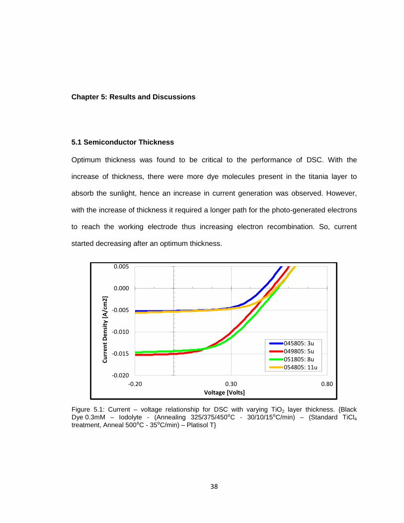
5.1 Semiconductor Thickness
Optimum thickness was found to be critical to the performance of DSC. With the
increase of thickness, there were more dye molecules present in the titania layer to
absorb the sunlight, hence an increase in current generation was observed. However,
with the increase of thickness it required a longer path for the photo-generated electrons
to reach the working electrode thus increasing electron recombination. So, current
started decreasing after an optimum thickness.
Figure 5.1: Current – voltage relationship for DSC with varying TiO2 layer thickness. Black
Dye 0.3mM – Iodolyte - (Annealing 325/375/450⁰C - 30/10/15⁰C/min) – (Standard TiCl4
treatment, Anneal 500⁰C - 35⁰C/min) – Platisol T
-0.020
-0.015
-0.010
-0.005
0.000
0.005
-0.20 0.30 0.80
Cu
rre
nt
De
nsi
ty [
A/c
m2
]
Voltage [Volts]
045805: 3u049805: 5u051805: 8u054805: 11u

39
Literatures suggested a slight decrease in open-circuit voltage with the increase in
thickness, but the change in observed voltage for the investigated thicknesses was
within the range of experimental error.
5.2 Porphyrin Dye
As an early part of the project, a group of push-pull (D--A) porphyrins were synthesized
and used to make DSCs. Methoxy group was used as electron donor and carboxylic
acid group as anchor. A free base without any metal (II-50), a zinc-based (II-92-1) and a
nickel-based (II-92-2) porphyrins were fabricated as a start. Two different concentrations
of the dye solution were investigated, and also a combination of the synthesized dyes,
denoted (I+II+III).
Table 5.1: DSC with varying TiO2 layer thickness.
Thickness (um)
ID Voc (V)
FF Jsc
(mA/cm2) Efficiency
(%)
3 045805 0.47 0.557 5.2 1.36
5 049805 0.51 0.394 15.05 3.02
8 051805 0.54 0.435 14.4 3.38
11 054805 0.53 0.548 5.34 1.54
Figure 5.2: Chemical structure of synthesized porphyrin dyes.

40
Only somewhat promising dye among the tested ones was Zn-based II-92-1, although
not comparable to the black dye. A little dependence on dye concentration was
observed, with a slight increase in performance. Nevertheless, from other experiments,
this difference became more subtle as the sensitization time was increased. The
homogeneous mixture of these 3 dyes was tested and not surprisingly, the resulting cell
performance resembled the mathematical average of the three individual cells.
Table 5.2: DSCs with synthesized porphyrin dyes.
Dye Dye Conc.
(mM) Voc (V)
FF Jsc
(mA/cm2) Efficiency
(%)
II-50 0.2 0.37 0.607 0.714 0.16
0.4 0.4 0.561 1.07 0.24
II-92-1 0.2 0.39 0.625 1.12 0.27
0.4 0.4 0.613 1.4 0.34
II-92-2 0.2 0.36 0.632 0.218 0.05
0.4 0.36 0.624 0.23 0.05
I+II+III 0.2 0.39 0.629 0.72 0.18
0.4 0.31 0.613 0.797 0.19
Black Dye 0.3 0.54 0.435 14.4 3.38
Figure 5.3: Quantum efficiency of DSCs made with porphyrin dyes.
0
5
10
15
20
25
30
400 450 500 550 600 650 700 750 800
Qu
antu
m E
ffic
ien
cy (
%)
Wavelength (nm)
II-50 II-92-1 II-92-2 I + II + III

41
UV-Vis spectra of the dyes (Fig. 5.4) showed a very high absorbance in UV to low
frequency of the visible range for the porphyrin dyes, but lacked in near infra-red region.
From similar analysis for Black dye (Fig. 5.5), its absorbance was observed not to be
very intense but expanded over the whole visible region more evenly.
Hence it could be concluded that light absorbance was not a problem with these dyes. It
should be the band alignment and charge transfer properties, which was the reason for
low efficiency for these porphyrin dyes.
Figure 5.4: UV-Vis spectra of synthesized porphyrin dyes.
Figure 5.5: UV-Vis spectra of commercial black dye. (4.98 x 10 -5
M in DCM).
0.00E+00
5.00E+04
1.00E+05
1.50E+05
2.00E+05
2.50E+05
3.00E+05
450 500 550 600 650 700
Mo
lar
ext
inct
ion
co
eff
icie
nt
(
Lmo
l-1
cm-1
)
Wavelength (nm)
II-50-free-base
II-92-1-ZnP
II-92-2-NiP
0.00E+00
1.00E+04
2.00E+04
3.00E+04
4.00E+04
5.00E+04
450 500 550 600 650 700 750
Mo
lar
ext
inct
ion
co
eff
icie
nt
(
Lmo
l-1
cm-1
)
Wavelength (nm)

42
The best reported dye in terms of solar cell efficiency so far is a Zn-based porphyrin dye
(Fig 3.3). Design criteria for efficient porphyrin dye are mentioned in section 3.2.10.
5.3 TiCl4 Treatment
An ultra-high purity TiO2 layer were deposited on the nanocrystalline titania by Chemical
Bath Deposition in 50mM aqueous TiCl4 solution for 30 min at 70⁰C, followed by a 450⁰C
thermal annealing. The solution concentration was varied to optimize the effect.
Table 5.3: Effect of TiCl4 treatment for DSC
TiCl4 Concentration
(mM)
Voc (V)
FF Jsc
(mA/cm2) ƞ (%)
Series Resistance (Ω/cm2)
0 0.52 0.558 4.3 1.25 35.9
20 0.53 0.546 6.5 1.88 27.8
50 0.47 0.552 8.9 2.3 15.3
Figure 5.6: Current – voltage relationship for DSC with different concentrations of TiCl4 treatment. Titania thickness 8um, (Annealing 325/375/450⁰C – 30/15/10⁰C/min), (TiCl4 treatment anneal
500⁰C - 30⁰C/min), Black Dye, Iodolyte, Platisol T
-0.010
-0.008
-0.006
-0.004
-0.002
0.000
0.002
0.004
-0.20 0.30 0.80
Cu
rre
nt
De
nsi
ty [
A/c
m2
]
Voltage [Volts]
059805: TiCl4 0mM058805: TiCl4 20mM062902: TiCl4 50mM

43
Any concentration higher than 50mM of TiCl4 for the treatment made the film to flake. As
the TiCl4 solution being slightly acidic in nature,62 at sufficient concentration it acted as
an etchant for TiO2 nanoparticles and could cause flaking. Incorporation of TiCl4
treatment increased the cell current. During thermal treatment the absorbed TiCl4 inside
the titania nanoparticles get oxidized and increased surface porosity causing improved
dye loading. Due to enhanced inter-particle necking and reduced charge recombination
(section 3.1.4), a decrease in series resistance and increase in short-circuit current were
observed with the incorporation of TiCl4 treatment and with increase of its concentration.
5.4 Blocking Layer
5.4.1 RF Sputtered Blocking Layer
A blocking layer of RF sputtered TiO2 was deposited on clean FTO glass. The sputtering
was done with a Titanium target, in presence of O2 (3.4mTorr) and Ar (6mTorr) at room
temperature. Incorporation of an RF sputtered blocking layer decreased both the current
and the voltage. With an increase in blocking layer thickness, more decrease is
observed.
Table 5.4: DSCs with different thickness of RF sputtered TiO2 blocking layer.
Blocking Layer
Thickness (nm) Cell ID Voc (V) FF
Jsc
(mA/cm2) ƞ (%)
0 nm 751110 0.67 0.486 12.96 4.22
20 nm 920120 0.63 0.536 10.77 3.63
50 nm 950120 0.63 0.532 10.39 3.54
100 nm 980120 0.61 0.521 9.96 3.17

44
5.4.2 Chemical Bath Deposition (CBD) Blocking Layer
An thin TiO2 blocking layer were deposited on the TCO substrate by Chemical Bath
Deposition in 50mM aqueous TiCl4 solution for 30 min at 70⁰C.
Figure 5.7: Current –voltage relationship for DSC with varying blocking layer thickness. Titania
thickness 8um, (Annealing 325/375/450/500⁰C - 5⁰C/min), (Standard TiCl4 treatment, Anneal
500⁰C - 30⁰C/min), Black Dye, Electrolyte I, Platisol T
-0.020
-0.015
-0.010
-0.005
0.000
0.005
-0.20 0.30 0.80
Cu
rre
nt
De
nsi
ty [
A/c
m2
]
Voltage [Volts]
751110: 0 nm920120: 20nm950120: 50nm980120: 120nm
Figure 5.8: Current –voltage relationship for DSC with and without CBD blocking layer. Titania
thickness 11um, (Annealing 325/375/450/500⁰C - 5⁰C/min), (Standard TiCl4 treatment, Anneal 500⁰C - 30⁰C/min), Black Dye, Electrolyte I, Platisol T
-0.015
-0.010
-0.005
0.000
0.005
-0.20 0.30 0.80
Cu
rre
nt
De
nsi
ty [
A/c
m2
]
Voltage [Volts]
821208: No TiCl4
831208: CBD TiCl4

45
Chemical Bath Deposition deposited the thinnest possible blocking layer, which also
decreased the current. The purpose of the blocking layer was to prevent charge
recombination at the semiconductor/electrode interface, by preventing the electrolyte
ions from reaching the electrode. However, for a titania film not optimized for porosity,
the nanoporous film itself could effectively block the electrolyte. In that case, introduction
of a blocking layer could just cause added series resistance reducing cell performance,
which was probably the situation in these experiments.
5.5 Porosity and Surface Area
TiO2 film porosity is the single most important parameter for DSC. In this study, thermal
and chemical manipulation of film porosity was investigated.
5.5.1 Thermal Processing
Annealing temperature profile plays an important role in the film porosity. Annealing of
titania in a stepped manner was found to have considerable effect on the nanoparticle
structure, and hence on cell performance. Stepped annealing produced highly porous
and smaller grain film; while un-stepped annealing produced compact and larger grain
size. From Scanning Electron Microscope (SEM) image of the annealed film, it was
obvious that stepped annealing produced smaller grains and highly porous surface (Fig.
5.9 a, b). Lower Voc (due to more charge recombination as the electrolyte can go into the
semiconductor film) and higher Jsc (due to more dye absorption on the titania surface)
Table 5.5: Comparison between DSC with and without CBD TiO2 blocking layer.
CBD Blocking
Layer
Voc (V)
FF Jsc
(mA/cm2) ƞ (%)
No TiCl4 0.68 0.555 10.94 4.13
TiCl4 0.68 0.585 9.59 3.81
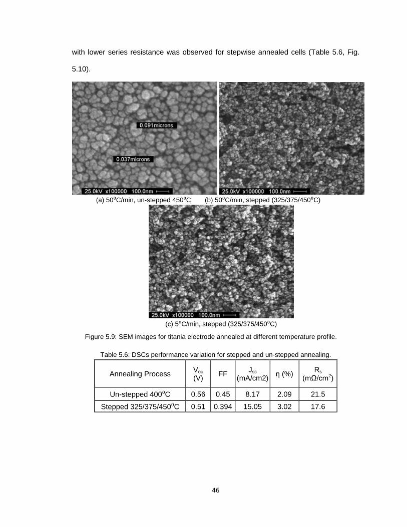
46
with lower series resistance was observed for stepwise annealed cells (Table 5.6, Fig.
5.10).
(a) 50⁰C/min, un-stepped 450⁰C (b) 50⁰C/min, stepped (325/375/450⁰C)
(c) 5⁰C/min, stepped (325/375/450⁰C)
Figure 5.9: SEM images for titania electrode annealed at different temperature profile.
Table 5.6: DSCs performance variation for stepped and un-stepped annealing.
Annealing Process Voc (V)
FF Jsc
(mA/cm2) ƞ (%)
Rs (mΩ/cm2)
Un-stepped 400⁰C 0.56 0.45 8.17 2.09 21.5
Stepped 325/375/450⁰C 0.51 0.394 15.05 3.02 17.6

47
Annealing temperature rise rate was found to have a boosting effect on cell
performance, although no discernible impact on titania structure could be observed from
SEM images (Fig. 5.9 b, c). However, current – voltage data of the cells (Table 5.7, Fig.
5.11) showed lower VOC and higher JSC with lower RS for cells annealed at faster rate.
The same trend was observed in the stepped annealing experiment for higher porosity
titania nanostructure. Thus, it was conclusive that higher annealing temperature rise rate
produced higher porosity film. However, slow rise rate allowed making higher thickness
TiO2 film without flaking, essential for high performance cells. For this reason, slower
annealing rate was used for subsequent experiments.
Figure 5.10: Current –voltage relationship for DSC with and without stepwise annealing. Titania thickness 5um, Standard TiCl4 treatment, Black Dye, Iodolyte, Platisol T
-0.020
-0.015
-0.010
-0.005
0.000
0.005
-0.20 0.00 0.20 0.40 0.60 0.80
Cu
rre
nt
De
nsi
ty [
A/c
m2
]
Voltage [Volts]
14021: Un-stepped Annealing49805: Stepped Annealing
Table 5.7: DSCs performance variation with annealing temperature rise rate.
Annealing Rate
Voc (V)
FF Jsc
(mA/cm2) ƞ (%)
Rs (mΩ/cm2)
50 C/min 0.64 0.521 12.14 4.05 17.3
5 C/min 0.67 0.518 10.63 3.69 18.5

48
5.5.2 Chemical Processing
Titanium dioxide nonporous film structure is highly dependent on the preparation
process, components and ambients. Film porosity is a function of Ethylene Glycol (EG)
or Polyethylene Glycol (PEG) content of the titania paste.
The vendor ‘Solaronix’ couldn’t disclose the paste content for business policy. EG and
PEG were mixed with the paste at different concentrations to alter film porosity. Adding
PEG at any concentration cracked the film; possibly being a powder, it didn’t mix
properly with the paste and put significant stress on the film while evaporating out during
sintering.
However, adding 12 wt% EG with the commercial Titania paste (0.1ml EG in 0.86g
paste) produced a highly porous film, possibly too porous as it reduced the current. SEM
image showed a high porosity film with large holes which is detrimental to cell
performance.
Figure 5.11: Current –voltage relationship for DSC annealed at different temperature rise rate.
Titania thickness 8um, Annealing 500⁰C, (Standard TiCl4 treatment, Anneal 500⁰C), Black Dye,
Electrolyte I, Platisol SP
-0.015
-0.010
-0.005
0.000
0.005
-0.20 0.00 0.20 0.40 0.60 0.80
Cu
rre
nt
De
nsi
ty [
A/c
m2
]
Voltage [Volts]
881208: 50C/min891208: 5C/min

49
Figure 5.12: SEM image of annealed titania film with 12 wt% EG
Figure 5.13: Current –voltage relationship for DSC with added EG to titania. Titania thickness
8um, (Annealing 325/375/450/500⁰C - 5⁰C/min), (Standard TiCl4 treatment, Anneal 500⁰C -
5⁰C/min), Black Dye, Electrolyte I, Platisol SP
-0.015
-0.010
-0.005
0.000
0.005
-0.20 0.00 0.20 0.40 0.60 0.80
Cu
rre
nt
De
nsi
ty [
A/c
m2
]
Voltage [Volts]
1070208: without EG1230208: with EG
Table 5.8: DSC performance with added ethylene glycol to alter surface porosity
Titania Voc (V)
FF Jsc
(mA/cm2) ƞ (%)
Series Resistance (Ω/cm2)
Commercial 0.59 0.479 9.39 2.65 39.4
With 12 wt% EG 0.59 0.581 7.27 2.49 31.9

50
5.6 Electrolyte
Two different electrolytes were studied and their performance in DSC was observed.
Commercial Electrolyte - Iodolyte Z150
Electrolyte I - LiI 0.1M, I2 - 0.05M, DMPII - 0.6M and Tert-Butyl Pyridine -
0.5M in Acetonitrile solvent.
DSC performance with Iodolyte was analyzed in Section 5.1. Similar experiment with
Electrolyte I revealed that it achieved a higher level of efficiency due to a 100mV higher
open circuit voltage, although the short-circuit current was lower (Table 5.9, Fig. 5.14).
Compared to Iodolyte, for ‘Electrolyte I’ the highest efficiency was also found at a higher
thickness, presumably due to the lower viscosity, which would allow it to penetrate deep
into the titania layer (Fig. 5.15). This deep penetration should also be the reason of lower
Jsc, as it would increase the probability of electron recombination with the electrolyte.
Figure 5.14: Current -voltage relationship for DSC with ‘Electrolyte I’ at difference thickness.
(Annealing 325/375/450/500⁰C - 5⁰C/min), (Standard TiCl4 treatment, Anneal 500⁰C - 35⁰C/min),
Black Dye, Electrolyte I, Platisol SP
-0.020
-0.015
-0.010
-0.005
0.000
0.005
-0.20 0.30 0.80
Cu
rre
nt
De
nsi
ty [
A/c
m2
]
Voltage [Volts]
751110: 8um
811208: 9um
821208:11um

51
5.7 Light Absorption
It was observed that putting a reflective mirror beneath a cell increased its efficiency by
increasing current. The fabricated solar cells also looked somewhat transparent. On a
typical 11um thick DSC placing a reflective mirror beneath the cell during current voltage
measurement showed a current increase of 9%, increasing the efficiency from 4.2% to
4.4% (Fig. 5.16).
Figure 5.15: Comparison between Iodolyte and Electrolyte I.
3.02
3.38
1.54 0
2
4
6
8
10
12
14
16
18
1.5
2
2.5
3
3.5
4
4.5
5 6 7 8 9 10 11
Jsc
(mA
/cm
2)
Effi
cie
ncy
(%
)
Titania Thickness (um)
Efficiency Iodolyte Efficiency Electrolyte I
Jsc Iodolyte Jsc Electrolyte I
Table 5.9: DSC with ‘Electrolyte I’ at difference thickness
Titania
Thickness (um)
Voc
(V) FF
Jsc
(mA/cm2) ƞ (%)
8 0.67 0.486 12.96 4.22
9 0.68 0.536 11.74 4.28
11 0.68 0.555 10.94 4.13
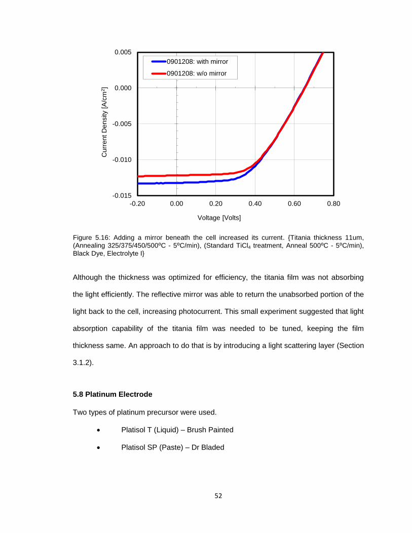
52
Although the thickness was optimized for efficiency, the titania film was not absorbing
the light efficiently. The reflective mirror was able to return the unabsorbed portion of the
light back to the cell, increasing photocurrent. This small experiment suggested that light
absorption capability of the titania film was needed to be tuned, keeping the film
thickness same. An approach to do that is by introducing a light scattering layer (Section
3.1.2).
5.8 Platinum Electrode
Two types of platinum precursor were used.
Platisol T (Liquid) – Brush Painted
Platisol SP (Paste) – Dr Bladed
Figure 5.16: Adding a mirror beneath the cell increased its current. Titania thickness 11um,
(Annealing 325/375/450/500⁰C - 5⁰C/min), (Standard TiCl4 treatment, Anneal 500⁰C - 5⁰C/min),
Black Dye, Electrolyte I
-0.015
-0.010
-0.005
0.000
0.005
-0.20 0.00 0.20 0.40 0.60 0.80
Curr
ent
Density
[A/c
m2]
Voltage [Volts]
0901208: with mirror
0901208: w/o mirror

53
Higher current as well as higher efficiency was observed for the paste precursor, as it
had more platinum content, thus provided more electron exchange center with the
electrolyte. The series resistance was also improved. (Table 5.10, Fig. 5.17)
The problem encountered with this paste was that the resultant Pt film was extremely
non-uniform & discontinuous (Fig. 5.18), which gave sheet resistances on the order of
hundreds of Ωs/sq, when applied on bare glass even when a thick layer of paste was
used. In the following experiment, a thick layer of Pt layer was applied by applying more
layers of Pt precursor and subsequent annealing. Thus, increasing the thickness of Pt
layer reduced the current, presumably due to the increase of series resistance.
(Table 5.11, Fig. 5.19)
Table 5.10: DSC with different platinum precursor
Platinum Electrode Voc (V)
FF Jsc
(mA/cm2) ƞ
(%) Rs
(Ω/cm2)
Platinum Paste 0.63 0.56 10.12 3.6 19.4
Platinum Solution 0.64 0.56 9.56 3.45 20.4
Figure 5.17: Performance comparison between DSC with platinum solution and platinum paste
precursor. Titania thickness 11um, (Annealing 325/375/450/500⁰C - 5⁰C/min), (Standard TiCl4
treatment, Anneal 500⁰C - 35⁰C/min), Black Dye, Electrolyte I
-0.015
-0.010
-0.005
0.000
0.005
-0.20 0.00 0.20 0.40 0.60 0.80
Cu
rre
nt
De
nsi
ty [
A/c
m2]
Voltage [Volts]
930128: Platisol T
940128: Platisol SP

54
Figure 5.18: SEM image of Pt deposited on FTO coated glass.
Table 5.11: DSC with increased platinum thickness.
Platinum Layer thickness
Voc (V)
FF Jsc
(mA/cm2) ƞ
(%)
3x 0.6 0.542 11.34 3.67
5x 0.6 0.549 10.95 3.58
Figure 5.19: Current –voltage relationship for DSC with different platinum thickness. Titania
thickness 9um, (Annealing 325/375/450⁰C – 30/10/15⁰C/min), (Standard TiCl4 treatment, Anneal
450⁰C - 5⁰C/min), Black Dye, Electrolyte I, Platisol SP
-0.015
-0.010
-0.005
0.000
0.005
-0.20 0.00 0.20 0.40 0.60 0.80
Cu
rre
nt
De
nsi
ty [
A/c
m2
]
Voltage [Volts]
4010607: Pt 3x4020607: Pt 5x

55
Chapter 6: Conclusion and Future Recommendations
This study explored several key parameters towards the optimization of DSC. The
conclusion is going to report some future recommendations for further research based
on the findings of this study.
As the Titania paste was applied by Dr Blading method, the resulting thickness was a
delicate function of the applied pressure, which was controlled manually. To obtain
better reproducibility, a screen printing technique may be introduced. The optimum film
porosity and surface area was not achieved. It is almost apparent that all different
temperature effects were investigated, and the underlying reason was probably chemical
components of the titania colloid. Either material from different vendor with different
specifications could be examined, or titania paste could be prepared at the laboratory.
For optimization of the titania structure, a measurement strategy for surface roughness,
effective surface area and film porosity is needed to be introduced. SEM data only gave
a raw insight to these parameters.
A light absorbing layer of 400nm diffuse TiO2 particle is needed. The need for a light
absorbing layer is corroborated by the fact that – by placing a mirror beneath the cell, the
short circuit current was found to increase. A sputtered platinum electrode may be
introduced, to improve charge collection as well as light absorption by reflecting the
unabsorbed light back with a mirror action. Some less important enhancements like -
soldered contact, anti-reflective coating and low sheet resistance substrates may also be
introduced.

56
References
1 M. Grätzel, Solar Energy Conversion by Dye-Sensitized Photovoltaic Cells, Inorg. Chem., 2005, 44(20), 6841–6851.
2 First Solar, Inc. (2012), First Solar, Inc. Announces fourth quarter and 2011 financial results (Press Release), Retrieved February 28, 2012 from http://investor.firstsolar.com/releasedetail.cfm?ReleaseID=652462
3 W. Shockley and H. J. Queisser, Detailed Balance Limit of Efficiency of p‐n Junction Solar Cells, J. Appl. Phys., 1961, 32, 510.
4 National Renewable Energy Laboratory (2012), Research Cell Efficiency Records, Retrieved September 01, 2012 from http://www.nrel.gov/ncpv/images/efficiency_chart.jpg
5 T. Marinado, K. Nonomura, J. Nissfolk, M. K. Karlsson, D. P. Hagberg, L. Sun, S. Mori, and A. Hagfeldt, How the Nature of Triphenylamine-Polyene Dyes in Dye-Sensitized Solar Cells Affects the Open-Circuit Voltage and Electron Lifetimes, Langmuir, 2010, 26, 2592
6 National Renewable Energy Laboratory (2012), Reference Solar Spectral Irradiance: Air Mass 1.5, Retrieved September 01, 2012 from http://rredc.nrel.gov/solar/spectra/am1.5/
7 M. Grätzel, Recent Advances in Sensitized Mesoscopic Solar Cells, Acc. Chem. Res., 2009, 42 (11), 1788-1798.
8 H. Tributsch, Reaction of Excited Chlorophyll Molecules at Electrodes and in Photosynthesis; Photochem. Photobiol., 1972, 16, 261-269.
9 N. Vlachopoulos, P. Liska, J. Augustynski,and M. Graetzel, Very efficient visible light energy harvesting and conversion by spectral sensitization of high surface area polycrystalline titanium dioxide films, J. Am. Chem. Soc., 1988, 110 (4), 1216–1220.
10 . O’Reagan and M. Gr t el, A Low-Cost, High-Efficiency Solar Cell Based on Dye Sensitized Colloidal TiO2 Films, Nature, 1991, 353, 737-740.
11 C. Chen, M. Wang, J. Li, N. Pootrakulchote, L. Alibabaei, C. Ngoc-le, J. Decoppet, J. Tsai, C. Grätzel, C. Wu, S. M. Zakeeruddin and M. Grätzel, Highly Efficient Light-Harvesting Ruthenium Sensitizer for Thin-Film Dye-Sensitized Solar Cells, ACS Nano, 2009, 3, 3103.

57
12 Y. Chiba, A. Islam, Y. Watanabe, R. Komiya, N. Koide and L. Han, Dye-Sensitized Solar Cells with Conversion Efficiency of 11.1%, Jpn. J. Appl. Phys., 2006, 45, L638.
13 A. Yella, H. Lee, H. Tsao, C. Yi, A. Chandiran, M. K. Nazeeruddin, E. Diau, C. Yeh, S. Zakeeruddin, M. Grätzel, Porphyrin-Sensitized Solar Cells with Cobalt (II/III)-Based Redox Electrolyte Exceed 12 Percent Efficiency, Science, 2011, 334, 629.
14 M. Grätzel, The Advent of Mesoscopic Injection Solar Cells, Progress in Photovoltaics: Research and Applications, 2006, 14(5), 429-442.
15 J. Barber and B. Andersson, Revealing the blueprint of photosynthesis, Nature, 1994, 370(6484), 31-34.
16 G. Rothenberger, D. Fitzmaurice and M. Grätzel, Spectroscopy of conduction band electrons in transparent metal oxide semiconductor films: optical determination of the flatband potential of colloidal titanium dioxide films, J. Phys. Chem, 1992, 96, 5983-5986.
17 C. J. Barbé, F. Arendse, P. Comte, M. Jirousek, F. Lenzmann, V. Shklover and M. Grätzel, Nanocrystalline Titanium Oxide Electrodes for Photovoltaic Applications, Journal of the American Ceramic Society, 1997, 80(12), 3157–3171.
18 Q. Wang, S. Ito, M. Grätzel, F. Fabregat-Santiago, I. Mora-Seró, J. Bisquert, T. Bessho, and H. Imai, Characteristics of High Efficiency Dye-Sensitized Solar Cells, J. Phys. Chem. B, 2006, 110(50), 25210–25221.
19 M. Zukalová, A. Zukal, L. Kavan, M. K. Nazeeruddin, P. Liska, and M. Grätzel, Organized Mesoporous TiO2 Films Exhibiting Greatly Enhanced Performance in Dye-Sensitized Solar Cells, Nano Lett., 2005, 5(9), 1789–1792.
20 T. Kang, A. P. Smith, B. E. Taylor, and M. F. Durstock, Fabrication of Highly-Ordered TiO2 Nanotube Arrays and Their Use in Dye-Sensitized Solar Cells, Nano Lett., 2009, 9(2), 601–606.
21 A. Hagfeldt, and M. Gratzel, Light-Induced redox reactions in nanocrystalline systems, Chem. Rev.,1995, 95, 49–68.
22 H. Rensmo, K. Keis, H. Lindström, S. Södergren, A. Solbrand, A. Hagfeldt, and S.E. Lindquist, High Light-to-Energy Conversion Efficiencies for Solar Cells Based on Nanostructured ZnO Electrodes, J. Phys. Chem. B, 1997, 101(14), 2598–2601.
23 A. Martinson, J. Elam, J. Hupp, and M. Pellin, ZnO Nanotube Based Dye-Sensitized Solar Cells; Nano Lett., 2007, 7(8), 2183–2187.
24 H. J. Snaith, and C. Ducati, SnO2-Based Dye-Sensitized Hybrid Solar Cells Exhibiting Near Unity Absorbed Photon-to-Electron Conversion Efficiency, Nano Lett., 2010, 10(4), 1259–1265.
25 R. Sharma, R. S. Mane, S. Min, and S. Han, Optimization of growth of In2O3 nano-spheres thin films by electrodeposition for dye-sensitized solar cells, Journal of Alloys and Compounds, 2009, 479(1-2), 840-843.

58
26 A. Kay, and M. Grätzel, Dye-Sensitized Core−Shell Nanocrystals: Improved Efficiency of Mesoporous Tin Oxide Electrodes Coated with a Thin Layer of an Insulating Oxide, Chem. Mater., 2002, 14(7), 2930–2935.
27 A. Le Viet, R. Jose, M. V. Reddy, B. V. R. Chowdari, and S. Ramakrishna, Nb2O5 Photoelectrodes for Dye-Sensitized Solar Cells: Choice of the Polymorph, J. Phys. Chem. C, 2010, 114(49), 21795–21800.
28 V. Shklover, M. K. Nazeeruddin, S. M. Zakeeruddin, C. Barbé, A. Kay, T. Haibach, W. Steurer, R. Hermann, H. U. Nissen, and M. Grätzel, Structure of Nanocrystalline TiO2 Powders and Precursor to Their Highly Efficient Photosensitizer, Chem. Mater., 1997, 9(2), 430–439.
29 S. Nakade, M. Matsuda, S. Kambe, Y. Saito, T. Kitamura, T. Sakata, Y. Wada, H. Mori, and S. Yanagida, Dependence of TiO2 Nanoparticle Preparation Methods and Annealing Temperature on the Efficiency of Dye-Sensitized Solar Cells, J. Phys. Chem. B, 2002, 106 (39), 10004-10010.
30 S. Nakade, Y. Saito, W. Kubo, T. Kitamura, Y. Wada, and S. Yanagida , Influence of TiO2 Nanoparticle Size on Electron Diffusion and Recombination in Dye-Sensitized TiO2 Solar Cells, J. Phys. Chem. B 2003, 107, 8607-8611.
31 M. K. Nazeeruddin, P. Péchy, T. Renouard, S. M. Zakeeruddin, R. Humphry-Baker, P. Comte, P. Liska, L. Cevey, E. Costa, V. Shklover, L. Spiccia, G. B. Deacon, C. A. Bignozzi, and M. Grätzel, Engineering of Efficient Panchromatic Sensitizers for Nanocrystalline TiO2-Based Solar Cells, J. Am. Chem. Soc., 2001, 123(8), 1613-1624.
32 M. Grätzel, Conversion of sunlight to electric power by nanocrystalline dye-sensitized solar cells, Journal of Photochemistry and Photobiology A: Chemistry, 2004, 164(1–3), 3-14.
33 S. Ito, M. K. Nazeeruddin, S. M. Zakeeruddin, P. P´echy, P. Comte, M. Gr¨atzel, T. Mizuno, A. Tanaka, and T. Koyanagi, Study of Dye-Sensitized Solar Cells by Scanning Electron Micrograph Observation and Thickness Optimization of Porous TiO2 Electrodes, International J. Photoenergy, 2009, 2009, 517609.
34 L. Meng, and C. Li, Blocking Layer Effect on Dye-Sensitized Solar Cells Assembled with TiO2 Nanorods Prepared by DC Reactive Magnetron Sputtering, Nanoscience and Nanotechnology Letters, 2011, 3(2), 181–185.
35 P. J. Cameron and L. M. Peter, Characterization of Titanium Dioxide Blocking Layers in Dye-Sensitized Nanocrystalline Solar Cells, J. Phys. Chem. B, 2003, 107, 14394-14400.
36 A. Burke, S. Ito, H. Snaith, U. Bach, J. Kwiatkowski, and M. Grätzel, The Function of a TiO2 Compact Layer in Dye-Sensitized Solar Cells Incorporating “Planar” Organic Dyes, Nano Lett., 2008, 8(4), 977–981.
37 S. Ito, T. N. Murakami, P. Comte, P. Liska, C. Grätzel, M. K. Nazeeruddin, M. Grätzel, Fabrication of thin film dye sensitized solar cells with solar to electric power conversion efficiency over 10%, Thin Solid Films, 2008, 516(14), 4613–4619.

59
38 H. Choi, C. Nahm, J. Kim, J. Moon, S. Nam, D. Jung, and B. Park, The effect of TiCl4-treated TiO2 compact layer on the performance of dye-sensitized solar cell, Current Applied Physics, 2012, 12(3), 737–741.
39 S. Ito, P. Liska, P. Comte, R. Charvet, P. Péchy, U. Bac, L. Schmidt-Mende, S. M. Zakeeruddin, A. Kay, M. K. Nazeeruddin, and M. Grätzel, Control of dark current in photoelectrochemical (TiO2/I
−- I3−) and dye-sensitized solar cells, Chem. Commun.,
2005, 34, 4351-4353.
40 E. Palomares, J. N. Clifford, S. A. Haque, T. Lutz, and J. R. Durrant, Control of Charge Recombination Dynamics in Dye Sensitized Solar Cells by the Use of Conformally Deposited Metal Oxide Blocking Layers, J. Am. Chem. Soc., 2003, 125(2), 475–482.
41 Z. Wang, T. Yamaguchi, H. Sugihara, and H. Arakawa, Significant Efficiency Improvement of the Black Dye-Sensitized Solar Cell through Protonation of TiO2 Films, Langmuir, 2005, 21(10), 4272–4276.
42 Y. V. Zubavichus, Y. L. Slovokhotov, M. K. Nazeeruddin, S. M. Zakeeruddin, M. Grätzel, and V. Shklover, Structural Characterization of Solar Cell Prototypes Based on Nanocrystalline TiO2 Anatase Sensitized with Ru Complexes. X-ray Diffraction, XPS, and XAFS Spectroscopy Study, Chem. Mater., 2002, 14(8), 3556–3563.
43 S. M. Zakeeruddin, M. K. Nazeeruddin, P. Pechy, F. P. Rotzinger, R. Humphry-Baker, K. Kalyanasundaram, M. Grätzel, V. Shklover and T. Haibach, Molecular Engineering of Photosensitizers for Nanocrystalline Solar Cells: Synthesis and Characterization of Ru Dyes Based on Phosphonated Terpyridines, Inorg. Chem., 1997, 36 (25), 5937–5946.
44 M. K. Nazeeruddin, P. Péchy, T. Renouard, S. M. Zakeeruddin, R. Humphry-Baker, P. Comte, P. Liska, L. Cevey, E. Costa, V. Shklover, L. Spiccia, G. B. Deacon, C. A. Bignozzi and M. Grätzel, Engineering of Efficient Panchromatic Sensitizers for Nanocrystalline TiO2-Based Solar Cells, J. Am. Chem. Soc., 2001, 123, 1613.
45 M. Grätzel, and J. Durrant, Dye-Sensitised Mesoscopic Solar Cells. In M. Archer and
A. Nozik (Eds.), Nanostructured And Photoelectrochemical Systems For Solar Photon Conversion (pp. 503-536), Imperial College Press.
46 M. K. Nazeeruddin, A. Kay, I. Rodicio, R. Humphry-Baker, E. Mueller, P. Liska, N. Vlachopoulos, M. Graetzel, Conversion of light to electricity by cis-X2bis(2,2'-bipyridyl-4,4'-dicarboxylate)ruthenium(II) charge-transfer sensitizers (X = Cl-, Br-, I-, CN-, and SCN-) on nanocrystalline titanium dioxide electrodes, J. Am. Chem. Soc., 1993, 115(14), 6382–6390.
47 M. K. Nazeeruddin, P. Péchy and M. Grätzel, Efficient panchromatic sensitization of nanocrystallineTiO2 films by a black dye based on a trithiocyanato–ruthenium complex, Chem. Commun., 1997, 18, 1705-1706.
48 M. K. Nazeeruddin, R. Humphry-Baker, P. Liska, and M. Grätzel, Investigation of Sensitizer Adsorption and the Influence of Protons on Current and Voltage of a Dye-Sensitized Nanocrystalline TiO2 Solar Cell, J. Phys. Chem. B, 2003, 107(34), 8981–8987.

60
49 M. K. Nazeeruddin, S. M. Zakeeruddin, R. Humphry-Baker, M. Jirousek, P. Liska, N. Vlachopoulos, V. Shklover, C. H. Fischer, and M. Grätzel, Acid−Base Equilibria of (2,2‘-Bipyridyl-4,4‘-dicarboxylic acid)ruthenium(II) Complexes and the Effect of Protonation on Charge-Transfer Sensitization of Nanocrystalline Titania, Inorg. Chem., 1999, 38(26), 6298–6305.
50 M. K. Nazeeruddin, R. Humphry-Baker, M. Grätzel, and B. A. Murrer, Efficient near IR sensitization of nanocrystalline TiO2 films by ruthenium phthalocyanines, Chem. Commun., 1998, 6, 719-720.
51 Q. Wang, W. M. Campbell, E. E. Bonfantani, K. W. Jolley, D. L. Officer, P. J. Walsh, K. Gordon, R. Humphry-Baker, M. K. Nazeeruddin, and M. Grätzel, Efficient Light Harvesting by Using Green Zn-Porphyrin-Sensitized Nanocrystalline TiO2 Films, J. Phys. Chem. B, 2005, 109(32), 15397–15409.
52 J. N. Clifford, E. Palomares, M. K. Nazeeruddin, M. Grätzel, J. Nelson, X. Li, N. J. Long, and J. R. Durrant, Molecular Control of Recombination Dynamics in Dye-Sensitized Nanocrystalline TiO2 Films: Free Energy vs Distance Dependence, J. Am. Chem. Soc., 2004, 126(16), 5225–5233.
53 J. Lagref, M. K. Nazeeruddin, and M. Grätzel, Molecular engineering on semiconductor surfaces: design, synthesis and application of new efficient amphiphilic ruthenium photosensitizers for nanocrystalline TiO2 solar cells, Synthetic Metals, 2003, 138, 333–339.
54 C. Klein, M. K. Nazeeruddin, D. Censo, P. Liska, and M. Grätzel, Amphiphilic Ruthenium Sensitizers and Their Applications in Dye-Sensitized Solar Cells, Inorg. Chem., 2004, 43(14), 4216–4226.
55 J. N. Clifford, E. Palomares, M. K. Nazeeruddin, R. Thampi, M. Grätzel, and J. R. Durrant, Multistep Electron Transfer Processes on Dye Co-sensitized Nanocrystalline TiO2 Films, J. Am. Chem. Soc., 2004, 126(18), 5670–5671.
56 M. K. Nazeeruddin, R. Humphry-Baker, D. L. Officer, W. M. Campbell, A. K. Burrell and M. Grätzel, Application of metalloporphyrins in nanocrystalline dye-sensitized solar cells for conversion of sunlight into electricity, Langmuir 20(15), 2004, 6514-6517.
57 Y. Chang, C. Wang, T. Pan, S. Hong, C. Lan, H. Kuo, C. Lo, H. Hsu, C. Lin, and E. Diau, A strategy to design highly efficient porphyrin sensitizers for dye-sensitized solar cells, Chem. Commun., 2011, 47, 8910-8912.
58 W. M. Campbell, K. W. Jolley, P. Wagner, K. Wagner, P. J. Walsh, K. C. Gordon, L. Schmidt-Mende, M. K. Nazeeruddin, Q. Wang, M. Grätzel, and D. L. Officer, Highly Efficient Porphyrin Sensitizers for Dye-Sensitized Solar Cells, J. Phys. Chem. C, 2007, 111(32), 11760–11762.
59 W. M. Campbell, A. K. Burrell, D. L. Officer, K. W. Jolley, Porphyrins as light harvesters in the dye-sensitised TiO2 solar cell, Coordination Chemistry Reviews, 2004, 248, 1363–1379.
60 J. Wu, Z. Lan, S. Hao, P. Li, J. Lin, M. Huang, L. Fang, and Y. Huang, Progress on the electrolytes for DSSC, Pure Appl. Chem., 2008, 80(11), 2241-2258.

61
61 L. Han, N. Koide, Y. Chiba, A. Islam, R. Komiya, N. Fuke, A. Fukui and R. Yamanaka, Improvement of efficiency of dye-sensitized solar cells by reduction of internal resistance, Appl Phys Lett, 2005, 86, 213501–213503.
62 L. Zeng, S. Dai, K. Wang, X. Pan, C. Shi, L. Guo, Mechanism of Enhanced
Performance of Dye-Sensitized Solar Cell Based TiO2 Films Treated by Titanium
Tetrachloride, Chinese Physics Letters, 2004, 21(9), 1835-1837.

62
Appendices

63
Appendix A: Image Copyright Information
Figure 1.1 : Reprinted from Research Cell Efficiency Records, NREL,
http://www.nrel.gov/ncpv/images/efficiency_chart.jpg (Retrieved September 01, 2012),
Copyright © 2012, with permission from National Renewable Energy Laboratory.
Figure 2.2 : Reprinted from J. Phys. Chem. B, Volume 110 (50), Pages
25210–25221, Q. Wang, S. Ito, M. Grätzel, F. Fabregat-Santiago, I. Mora-Seró, J.
Bisquert, T. Bessho, and H. Imai, Characteristics of High Efficiency Dye-Sensitized Solar
Cells, Copyright © 2006, with permission from American Chemical Society.
Figure 3.2 : Reprinted from Dye-Sensitised Mesoscopic Solar Cells, M.
Grätzel, and J. Durrant, in Nanostructured And Photoelectrochemical Systems For Solar
Photon Conversion, M. Archer and A. Nozik (Eds.), pp. 503-536, Copyright © 2008
Imperial College Press.
Figure 3.3 : Reprinted from Ruthenizer 620-1H3TBA, Solaronix SA,
http://www.solaronix.com/products/rutheniumdyes/ruthenizer6201h3tba/ (Retrieved
September 07, 2012), Copyright © 2012, with permission from Solaronix SA.
Figure 3.4 : Reprinted from Science, Volume 334, No. 6056, Pages 629-634,
A. Yella, H. Lee, H. Tsao, C. Yi, A. Chandiran, M. K. Nazeeruddin, E. Diau, C. Yeh, S.
Zakeeruddin, and M. Grätzel, Porphyrin-Sensitized Solar Cells with Cobalt (II/III)-Based
Redox Electrolyte Exceed 12 Percent Efficiency, Copyright © 2011, with permission from
AAAS.
Figure 3.5 : Reprinted from Journal of Photochemistry and Photobiology A:
Chemistry, Volume 164, Issues 1–3, Pages 3–14, Michael Grätzel, Conversion of
sunlight to electric power by nanocrystalline dye sensitized solar cells, Copyright © 2004,
with permission from Elsevier.