A Study on Shunt Resistor-based Current Measurements for ...
7
HAL Id: hal-02405883 https://hal.archives-ouvertes.fr/hal-02405883 Submitted on 11 Dec 2019 HAL is a multi-disciplinary open access archive for the deposit and dissemination of sci- entific research documents, whether they are pub- lished or not. The documents may come from teaching and research institutions in France or abroad, or from public or private research centers. L’archive ouverte pluridisciplinaire HAL, est destinée au dépôt et à la diffusion de documents scientifiques de niveau recherche, publiés ou non, émanant des établissements d’enseignement et de recherche français ou étrangers, des laboratoires publics ou privés. A Study on Shunt Resistor-based Current Measurements for Fast Switching GaN Devices Thilini Wickramasinghe, Bruno Allard, Cyril Buttay, Charles Joubert, Christian Martin, Jean-Fraçois Mogniotte, Hervé Morel, Pascal Bevilacqua, Thanh-Long Le, Stephane Azzopardi To cite this version: Thilini Wickramasinghe, Bruno Allard, Cyril Buttay, Charles Joubert, Christian Martin, et al.. A Study on Shunt Resistor-based Current Measurements for Fast Switching GaN Devices. 45th IEEE IECON, Oct 2019, Lisbonne, Portugal. hal-02405883
Transcript of A Study on Shunt Resistor-based Current Measurements for ...

HAL Id: hal-02405883https://hal.archives-ouvertes.fr/hal-02405883
Submitted on 11 Dec 2019
HAL is a multi-disciplinary open accessarchive for the deposit and dissemination of sci-entific research documents, whether they are pub-lished or not. The documents may come fromteaching and research institutions in France orabroad, or from public or private research centers.
L’archive ouverte pluridisciplinaire HAL, estdestinée au dépôt et à la diffusion de documentsscientifiques de niveau recherche, publiés ou non,émanant des établissements d’enseignement et derecherche français ou étrangers, des laboratoirespublics ou privés.
A Study on Shunt Resistor-based CurrentMeasurements for Fast Switching GaN Devices
Thilini Wickramasinghe, Bruno Allard, Cyril Buttay, Charles Joubert,Christian Martin, Jean-Fraçois Mogniotte, Hervé Morel, Pascal Bevilacqua,
Thanh-Long Le, Stephane Azzopardi
To cite this version:Thilini Wickramasinghe, Bruno Allard, Cyril Buttay, Charles Joubert, Christian Martin, et al.. AStudy on Shunt Resistor-based Current Measurements for Fast Switching GaN Devices. 45th IEEEIECON, Oct 2019, Lisbonne, Portugal. hal-02405883

A Study on Shunt Resistor-based CurrentMeasurements for Fast Switching GaN Devices
Thilini Wickramasinghe1, Bruno Allard1, Cyril Buttay1, Charles Joubert1, Christian Martin1,
Jean-Fracois Mogniotte1, Herve Morel1, Pascal Bevilacqua1, Thanh-Long Le2, Stephane Azzopardi21Univ Lyon, Universite Claude Bernard Lyon 1, INSA Lyon, CNRS, Ampere, F-69621, Villeurbanne, France.
2Electrical & Electronics Division, Safran Tech - Safran Paris Saclay, [email protected]
Abstract—Current viewing resistor (CVR) based measurementof a high frequency switching cell is presented. The draincurrent of the low-side GaN HEMT switch was measured at100 kHz switching frequency for a maximum load current of8 A and a dc input of 80 V. To analyze the results, bothsimulations and experiments were used. The parasitic elements ofthe PCB layout (i.e. calculated using the Ansys-Q3D Extractorsoftware) were included in the simulation model. This paperexplains the consequences of mounting CVRs in the common-source path of transistors compared to a circuit without a CVR.Simulation results are found to be in very good agreementwith measurements. Hence, the simulation model can be usedto estimate the current waveforms when it is not desirable toresort to intrusive measurement methods.
Index Terms—CVR, GaN HEMT, high frequency, currentmeasurements
I. INTRODUCTION
Wide bandgap semiconductor materials enable power tran-sistors to operate at high frequencies, high voltages and at hightemperatures. In particular, Gallium Nitride (GaN) is attractiveto build high electron-mobility transistors (HEMTs). Theyoffer higher power density and lower on-resistance over siliconbased counterparts. Therefore, lower losses are expected witha favourable impact on the heat dissipation strategy with a gainin mass. Due to a relatively stable threshold voltage over therange of 25o to 150o C and the positive temperature coefficientof the on-resistance, GaN HEMTs are more desirable forparallel configurations. However, a slight mismatch in thethreshold voltage from one device to another may degradethe current distribution during switching. These circumstancesare especially concerning as the GaN HEMTs have very fastswitching times (with few tens of nanoseconds) and largeoscillations may arise during transients.
To apply them in practical situations, it is important toexamine the switching behaviour in order to identify andcontrol these high current-voltage transients. However, thesecurrent waveforms are particularly difficult to measure withoutdisturbing the behaviour of the circuit.
There are many current measuring concepts based on somebasic physical principles [1], [2]. Most of the novel sensorsare incorporated with digital signal processing technologiesto achieve greater noise immunity and stringent design con-straints of a printed circuit board (PCB).Primarily, the current sensor (CS) techniques are based on;
• Shunt resistor-based transducers [3]– [5].• Magnetic induction-based transducers (Rogowski coils,
current transformers) [8]– [9].• Magnetic-field based transducers (Hall effect, flux gate,
magnetoresistive—MR) [10].
In general, shunt resistor-based CSs (SR-CS) are simple,highly linear and cost effective but they do not providegalvanic isolation [3]– [5]; whereas magnetic induction orfield-based CSs are galvanically isolated [8]– [10]. However,compared to high-performance SR-CS (such as coaxial shunts)the bandwidth of Rogowski coil CSs is 10–100 times smallerand they introduce delays. Furthermore, the Rogowski coilscannot sense DC or low frequency currents.
Transformer-based CSs are applicable only for AC or highfrequency pulse current. Planar transformers with high powerare available for on-board integration [11], however, they arephysically larger than other CSs.
Compared to the SR-CSs, the hall effect sensors and thefluxgate suffer from imperfections due to offset and gain driftunder temperature. The dynamic response of a magnetoresis-tive (MR) CS is faster than a hall-based alternative sensor.However, it requires specific layout in designing primary busbar to measure MR-based current, which is challenging in acompact design [12].
Fig. 1. A comparison of shunt resistor technologies (adapted from [4])

Figure 1 illustrates some commonly used CS resistor typeswith a comparison of the rated power against both resistorvalue and temperature coefficient [4]. As illustrated in Fig. 1,metal strips, high power exposed element-based devices andcoaxial shunts resistors exhibit better temperature coefficientthan that of a current sense metal alloy. However, the highpower resistors are larger than the current sense metal alloyand they have parasitic inductances in the order of tensof nanohenries. Materials with high density (high thermalcapacity and low specific heat) reduce the size of the resistorand are suitable for compact applications.
The coaxial shunts (also known as current viewingresistors—CVR) are suitable for high-frequency measurementsdespite of the constraints in their continuous operations thatcan cause thermal issues, and relatively large dimensions. Theyhave extremely flat frequency response from DC to 2 GHz,present high performance in rise time and in accuracy. TheCVRs are noise immune and have fast response for highcurrent measurements (e.g. 5 kA with a 20 ns rise time) [6].They have no offset and do not require an auxiliary powersupply.
This paper presents a study on current measurements ofa high frequency GaN device using a CVR. An experiment-based analysis was conducted to investigate the impact ofmounting a shunt resistor in the power commutation path.For further evaluations, a simulation model of the circuit wasused. The Section II describes about a coaxial shunt resistor-based current sensor followed by basic configurations of atest prototype. The experiment setup, test conditions and theexperimental results are detailed in Section III. In Section IV,an analysis of the experiment and simulation results arepresented. Practical issues and suggestions to address thoseissues are described in Section V with a conclusion.
II. CURRENT VIEWING SHUNT RESISTOR-BASEDMEASUREMENTS
Illustrated in Fig. 2(a) is a simplified equivalent circuit ofa shunt resistor. Here, Rcs is the rated resistance while rsand Ls are parasitic resistance and inductance respectively.The parasitic inductance in the CVR limits the operationbandwidth. To minimize the uncertainty of the resistor value,the voltage across the CVR is measured by Kelvin bridgeconnections.
Selection of an appropriate power rating of a resistor ismade according to its joule losses (I2R, where I is themaximum continuous current requirement of the applicationand R is nominal resistance). To reduce power dissipation,smaller resistor values are preferred. Shunt resistors with verylow inductance or CVRs are being used in high frequencyapplications [5].
For this study, a lead connection type CVR with 25 mΩresistance [15] shown in Fig. 2 was used. A 2.5 W capableCVR is sufficient for a case of maximum current of 10 A.The impedance measurement of the CVR (i.e. SDN-414-025from TandM Research) in Fig. 3 depicts a low inductance in
the device with short length, approximately 6.6 nH at highfrequency range.
sL
sr
csRRcsv
loadi
supplyvsL
sr
csR
(a) (b)
Fig. 2. CVR: (a) simplified circuit model of CVR, (b) SDN-414-025 fromTandM Research [15].
105
106
107
108
frequency (Hz)
0.01
0.02
0.03
0.04
0.05
Rs
()
105
106
107
108
frequency (Hz)
10-2
100
|Z| (
) Impedance (Zcs
)
Resistance (Rs)
105 106 107 1080
50
100
teta
(d
eg
.)
105
106
107
108
Frequency (Hz)
6
8
10
12
Ls
(nH
)
Inductance (Ls)
Phase angle ( )
Fig. 3. Frequency response of SDN-414-025 from TandM Research, measuredby 4294A precision impedance analyzer.
A. An overview and the experimental prototype
The main objectives of the experiment are to obtain CVR-based current measurements at high frequency operation andto observe the effect of inserting a CVR in the power path. Toachieve them, two test cases are considered: case 1– prototypewith the CVR and case 2– CVR unmounted prototype. Acomparison of the voltage and current waveforms of the twocases can be used to observe the deviations. For the case 2,the current measurements can be predicted by a simulationmodel. Therefore, a precise model is essential for reliability ofthe study. This can be validated by replicating the experimentresults.
The basic configuration of the test circuit is a half-bridgeconverter built with a GaN HEMT as the low-side switchand a Schottky diode in the high-side. Figure 4 illustrates aschematic diagram of the prototype with the CVR. For non-isolated probe measurements, the best position is to mount
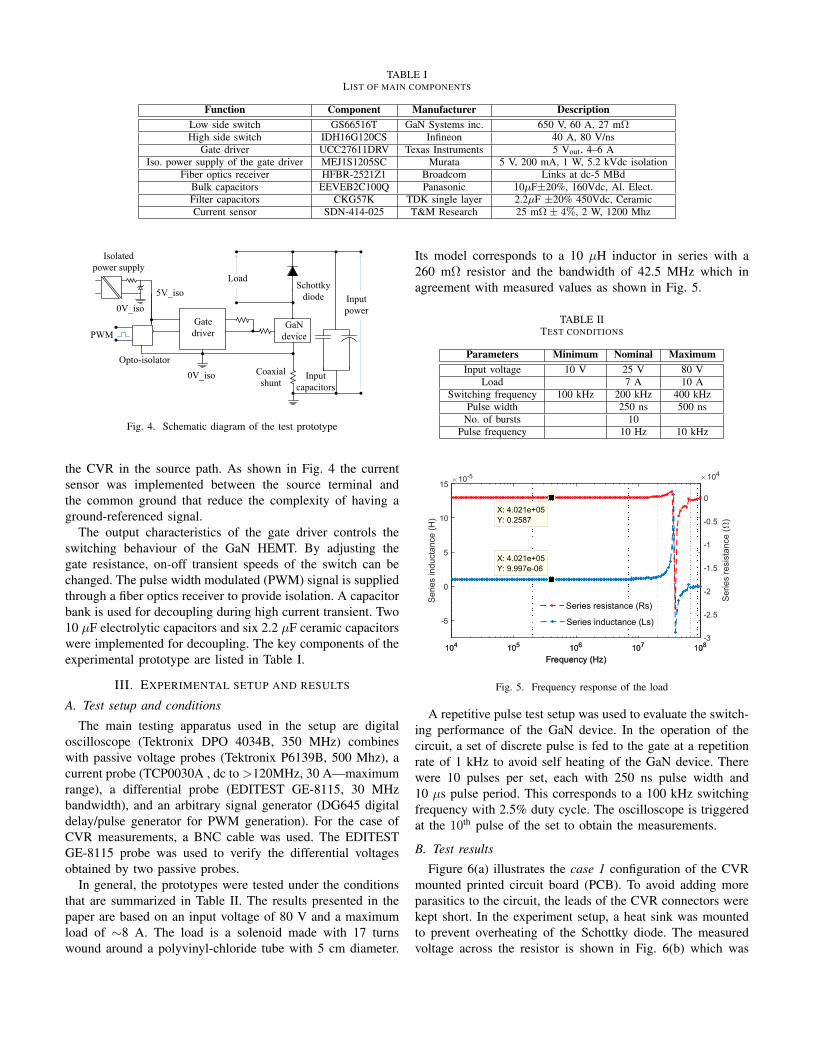
TABLE ILIST OF MAIN COMPONENTS
Function Component Manufacturer DescriptionLow side switch GS66516T GaN Systems inc. 650 V, 60 A, 27 mΩHigh side switch IDH16G120CS Infineon 40 A, 80 V/ns
Gate driver UCC27611DRV Texas Instruments 5 Vout, 4–6 AIso. power supply of the gate driver MEJ1S1205SC Murata 5 V, 200 mA, 1 W, 5.2 kVdc isolation
Fiber optics receiver HFBR-2521Z1 Broadcom Links at dc-5 MBdBulk capacitors EEVEB2C100Q Panasonic 10µF±20%, 160Vdc, Al. Elect.Filter capacitors CKG57K TDK single layer 2.2µF ±20% 450Vdc, CeramicCurrent sensor SDN-414-025 T&M Research 25 mΩ ± 4%, 2 W, 1200 Mhz
a
Fig. 4. Schematic diagram of the test prototype
the CVR in the source path. As shown in Fig. 4 the currentsensor was implemented between the source terminal andthe common ground that reduce the complexity of having aground-referenced signal.
The output characteristics of the gate driver controls theswitching behaviour of the GaN HEMT. By adjusting thegate resistance, on-off transient speeds of the switch can bechanged. The pulse width modulated (PWM) signal is suppliedthrough a fiber optics receiver to provide isolation. A capacitorbank is used for decoupling during high current transient. Two10 µF electrolytic capacitors and six 2.2 µF ceramic capacitorswere implemented for decoupling. The key components of theexperimental prototype are listed in Table I.
III. EXPERIMENTAL SETUP AND RESULTS
A. Test setup and conditions
The main testing apparatus used in the setup are digitaloscilloscope (Tektronix DPO 4034B, 350 MHz) combineswith passive voltage probes (Tektronix P6139B, 500 Mhz), acurrent probe (TCP0030A , dc to >120MHz, 30 A—maximumrange), a differential probe (EDITEST GE-8115, 30 MHzbandwidth), and an arbitrary signal generator (DG645 digitaldelay/pulse generator for PWM generation). For the case ofCVR measurements, a BNC cable was used. The EDITESTGE-8115 probe was used to verify the differential voltagesobtained by two passive probes.
In general, the prototypes were tested under the conditionsthat are summarized in Table II. The results presented in thepaper are based on an input voltage of 80 V and a maximumload of ∼8 A. The load is a solenoid made with 17 turnswound around a polyvinyl-chloride tube with 5 cm diameter.
Its model corresponds to a 10 µH inductor in series with a260 mΩ resistor and the bandwidth of 42.5 MHz which inagreement with measured values as shown in Fig. 5.
TABLE IITEST CONDITIONS
Parameters Minimum Nominal MaximumInput voltage 10 V 25 V 80 V
Load 7 A 10 ASwitching frequency 100 kHz 200 kHz 400 kHz
Pulse width 250 ns 500 nsNo. of bursts 10
Pulse frequency 10 Hz 10 kHz
104 105 106 107 108
Frequency (Hz)
-3
-2.5
-2
-1.5
-1
-0.5
0
Series r
esis
tance (
)
104
104 105 106 107 108
Frequency (Hz)
-5
0
5
10
15
Series induct
ance (
H)
10-5
Series inductance (Ls)
Series resistance (Rs)
X: 4.021e+05
Y: 9.997e-06
X: 4.021e+05
Y: 0.2587
Fig. 5. Frequency response of the load
A repetitive pulse test setup was used to evaluate the switch-ing performance of the GaN device. In the operation of thecircuit, a set of discrete pulse is fed to the gate at a repetitionrate of 1 kHz to avoid self heating of the GaN device. Therewere 10 pulses per set, each with 250 ns pulse width and10 µs pulse period. This corresponds to a 100 kHz switchingfrequency with 2.5% duty cycle. The oscilloscope is triggeredat the 10th pulse of the set to obtain the measurements.
B. Test results
Figure 6(a) illustrates the case 1 configuration of the CVRmounted printed circuit board (PCB). To avoid adding moreparasitics to the circuit, the leads of the CVR connectors werekept short. In the experiment setup, a heat sink was mountedto prevent overheating of the Schottky diode. The measuredvoltage across the resistor is shown in Fig. 6(b) which was
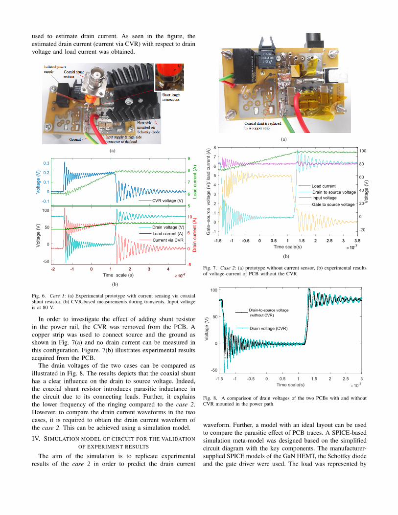
used to estimate drain current. As seen in the figure, theestimated drain current (current via CVR) with respect to drainvoltage and load current was obtained.
(a)
-2 -1 0 1 2 3 4
Time scale (s) 10-7
-0.1
0
0.1
0.2
0.3
Vo
lta
ge
(V
)
-2 -1 0 1 2 3 4
10-7
-5
0
5
10
Dra
in c
urr
en
t (A
)
-2 -1 0 1 2 3 4
Time scale (s) 10-7
5
6
7
8
9
Lo
ad
cu
rre
nt
(A)
Load current (A)
CVR voltage (V)
-2 -1 0 1 2 3 4
Time scale (s) 10-7
-50
0
50
100
Volta
ge
(V
)
Drain voltage (V)
Current via CVR
Load current (A)
(b)
Fig. 6. Case 1: (a) Experimental prototype with current sensing via coaxialshunt resistor. (b) CVR-based measurements during transients. Input voltageis at 80 V.
In order to investigate the effect of adding shunt resistorin the power rail, the CVR was removed from the PCB. Acopper strip was used to connect source and the ground asshown in Fig. 7(a) and no drain current can be measured inthis configuration. Figure. 7(b) illustrates experimental resultsacquired from the PCB.
The drain voltages of the two cases can be compared asillustrated in Fig. 8. The results depicts that the coaxial shunthas a clear influence on the drain to source voltage. Indeed,the coaxial shunt resistor introduces parasitic inductance inthe circuit due to its connecting leads. Further, it explainsthe lower frequency of the ringing compared to the case 2.However, to compare the drain current waveforms in the twocases, it is required to obtain the drain current waveform ofthe case 2. This can be achieved using a simulation model.
IV. SIMULATION MODEL OF CIRCUIT FOR THE VALIDATIONOF EXPERIMENT RESULTS
The aim of the simulation is to replicate experimentalresults of the case 2 in order to predict the drain current
(a)
-1.5 -1 -0.5 0 0.5 1 1.5 2 2.5 3 3.5
10-7
-20
0
20
40
60
80
100
Vo
lta
ge
(V
)
-1.5 -1 -0.5 0 0.5 1 1.5 2 2.5 3 3.5
Time scale(s) 10-7
-1
0
1
2
3
4
5
6
7
8
Ga
te--
so
urc
e
volta
ge
(V
)/ lo
ad
cu
rre
nt
(A)
Gate to source voltage
Load current
Drain to source voltage
Input voltage
(b)
Fig. 7. Case 2: (a) prototype without current sensor, (b) experimental resultsof voltage-current of PCB without the CVR
-1.5 -1 -0.5 0 0.5 1 1.5 2 2.5 3
Time scale(s) 10-7
-50
0
50
100
Vo
lta
ge
(V
)
Drain-to-source voltage
(without CVR)
Drain voltage (CVR)
Fig. 8. A comparison of drain voltages of the two PCBs with and withoutCVR mounted in the power path.
waveform. Further, a model with an ideal layout can be usedto compare the parasitic effect of PCB traces. A SPICE-basedsimulation meta-model was designed based on the simplifiedcircuit diagram with the key components. The manufacturer-supplied SPICE models of the GaN HEMT, the Schottky diodeand the gate driver were used. The load was represented by

an inductor connected in parallel with a parasitic capacitor.Further, the parasitic elements of the decoupling capacitorswere included to their models.
For the extraction of the PCB layout parasitics, the Ansys-Q3D software was used. Figure 9(a) illustrates the simplifieddiagram of the parasitic components considered for this case.In this circuit, both power and the control commutation pathsare in the same side of a single layer configuration. The par-asitics between the gate and gate-driver output is insignificantdue the compact design as seen in Fig 9(b). Therefore, theparasitics in this path can be neglected.
The values of parasitic components corresponding to thePCB traces were calculated using Ansis-Q3D software. Theywere included in the SPICE meta-model as seen in Fig. 10.For better fitting with the experiment curves, some of thesevalues were slightly adjusted. The estimated resistance of thecopper strip used in case 2 is approximately 0.15 mΩ, wherethe length, thickness and the width are respectively 11 mm,5 mm and 0.254 mm.
1gateR
2gateR
6Z
1Z
2Z
3Z
4Z
8Z
7Z
5Z
1Z
2Z
3Z
4Z
5Z
1gateR
2gateR
1Z
2Z3Z
4Z
5Z
1gateR
2gateR 6Z
(a) (b)
Fig. 9. Consideration of parasitic components: (a) simplified circuit modelwith consideration of parasitics in the layout, (b) the GaN HEMT and driveron the PCB.
The simulation results of the case 2 are compared withits experiments as shown in Fig. 11. The inclusion of straycapacitors of the PCB (i.e. Cx1, Cx2 and Cx3) made thesimulation results more comparable to its experiments. Theoutcome of the approach indicates that the simulation resultsduring transients are in fair agreement with its experiments topredict the drain current waveform.
The manufacturer provides three different models forGS66516T HEMT [16]. The basic model represents the elec-trical characteristics while the second and the third models arecomprised with thermal characteristics, and stray inductancesrespectively. All three models were studied by comparingthe results of simulations with the experiments. For thisapplication, there was no substantial difference in the outcomeprovided that the absent device parasitics are incorporatedexternally.
Fig. 10. LTSpice meta-model of double-pulse GaN HEMT circuit withoutmounting a CVR
2 4 6 8 10
Time (s) 10-8
-20
0
20
40
60
80
100V
olta
ge (
V)
Input voltage (sim)
Drain-source voltage (sim)
Drain-source
voltage (measured)
Input voltage (measured)
On transient
(a)
2.5 3 3.5 4 4.5 5
Time (s) 10-7
-20
0
20
40
60
80
100
Vo
ltag
e (
V)
Input voltage (sim)
Drain-source voltage (sim)
Drain-source
voltage (measured)
Input voltage (measured)
Off transient
(b)
0.5 1 1.5 2 2.5 3 3.5 4 4.5 5
Time (s) 10-7
0
2
4
6
8
Ga
te--
so
urc
e
vo
ltag
e (
V)/
loa
d c
urr
en
t (A
)
Gate to source voltage (sim)
Load current (sim)
Load current (measured)
Gate to source voltage (measured)
(c)
Fig. 11. Comparison of results of the case 2 SPICE simulation model. Nocurrent sensing resistor is implemented in this circuit.
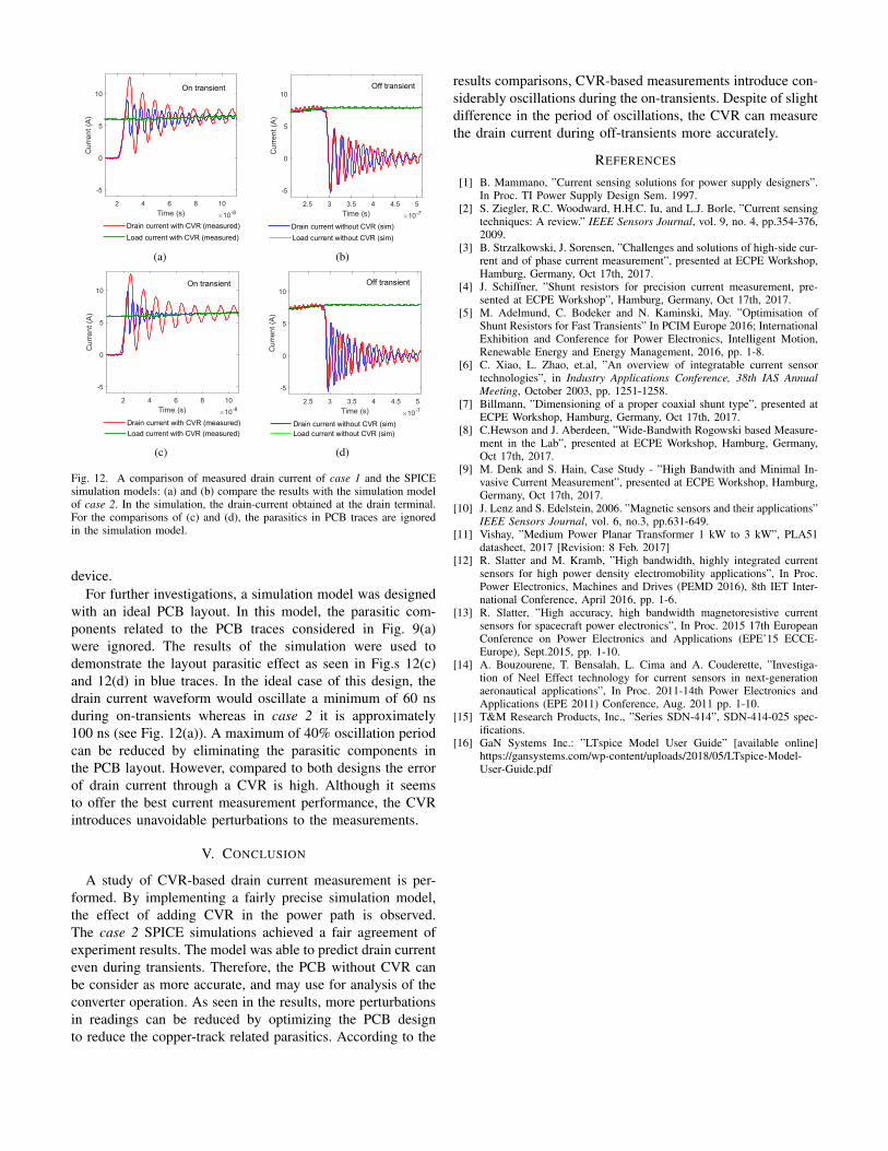
Figures 12(a) and (b) illustrate a comparison of CVR-basedcurrent measurements in case 1 with the simulation results ofcase 2. Both load and the drain currents are compared duringon and off transients. As seen in the figure, the oscillations ofthe measured drain current during the on-transients are highercompared to a predicted results of case 2. This confirms thatmeasuring drain current using a CVR adds error to the read-ings. Besides, low frequency oscillations in the measurementscan lead to inaccurate estimations of power dissipation in the
2 4 6 8 10
Time (s) 10-8
-5
0
5
10C
urr
en
t (A
)
Drain current with CVR (measured)
Load current with CVR (measured)
On transient
(a)
2.5 3 3.5 4 4.5 5
Time (s) 10-7
-5
0
5
10
Cu
rren
t (A
)
Drain current without CVR (sim)
Load current without CVR (sim)
Off transient
(b)
2 4 6 8 10
Time (s) 10-8
-5
0
5
10
Cu
rren
t (A
)
Drain current with CVR (measured)
Load current with CVR (measured)
On transient
(c)
2.5 3 3.5 4 4.5 5
Time (s) 10-7
-5
0
5
10
Cu
rren
t (A
)
Drain current without CVR (sim)
Load current without CVR (sim)
Off transient
(d)
Fig. 12. A comparison of measured drain current of case 1 and the SPICEsimulation models: (a) and (b) compare the results with the simulation modelof case 2. In the simulation, the drain-current obtained at the drain terminal.For the comparisons of (c) and (d), the parasitics in PCB traces are ignoredin the simulation model.
device.For further investigations, a simulation model was designed
with an ideal PCB layout. In this model, the parasitic com-ponents related to the PCB traces considered in Fig. 9(a)were ignored. The results of the simulation were used todemonstrate the layout parasitic effect as seen in Fig.s 12(c)and 12(d) in blue traces. In the ideal case of this design, thedrain current waveform would oscillate a minimum of 60 nsduring on-transients whereas in case 2 it is approximately100 ns (see Fig. 12(a)). A maximum of 40% oscillation periodcan be reduced by eliminating the parasitic components inthe PCB layout. However, compared to both designs the errorof drain current through a CVR is high. Although it seemsto offer the best current measurement performance, the CVRintroduces unavoidable perturbations to the measurements.
V. CONCLUSION
A study of CVR-based drain current measurement is per-formed. By implementing a fairly precise simulation model,the effect of adding CVR in the power path is observed.The case 2 SPICE simulations achieved a fair agreement ofexperiment results. The model was able to predict drain currenteven during transients. Therefore, the PCB without CVR canbe consider as more accurate, and may use for analysis of theconverter operation. As seen in the results, more perturbationsin readings can be reduced by optimizing the PCB designto reduce the copper-track related parasitics. According to the
results comparisons, CVR-based measurements introduce con-siderably oscillations during the on-transients. Despite of slightdifference in the period of oscillations, the CVR can measurethe drain current during off-transients more accurately.
REFERENCES
[1] B. Mammano, ”Current sensing solutions for power supply designers”.In Proc. TI Power Supply Design Sem. 1997.
[2] S. Ziegler, R.C. Woodward, H.H.C. Iu, and L.J. Borle, ”Current sensingtechniques: A review.” IEEE Sensors Journal, vol. 9, no. 4, pp.354-376,2009.
[3] B. Strzalkowski, J. Sorensen, ”Challenges and solutions of high-side cur-rent and of phase current measurement”, presented at ECPE Workshop,Hamburg, Germany, Oct 17th, 2017.
[4] J. Schiffner, ”Shunt resistors for precision current measurement, pre-sented at ECPE Workshop”, Hamburg, Germany, Oct 17th, 2017.
[5] M. Adelmund, C. Bodeker and N. Kaminski, May. ”Optimisation ofShunt Resistors for Fast Transients” In PCIM Europe 2016; InternationalExhibition and Conference for Power Electronics, Intelligent Motion,Renewable Energy and Energy Management, 2016, pp. 1-8.
[6] C. Xiao, L. Zhao, et.al, ”An overview of integratable current sensortechnologies”, in Industry Applications Conference, 38th IAS AnnualMeeting, October 2003, pp. 1251-1258.
[7] Billmann, ”Dimensioning of a proper coaxial shunt type”, presented atECPE Workshop, Hamburg, Germany, Oct 17th, 2017.
[8] C.Hewson and J. Aberdeen, ”Wide-Bandwith Rogowski based Measure-ment in the Lab”, presented at ECPE Workshop, Hamburg, Germany,Oct 17th, 2017.
[9] M. Denk and S. Hain, Case Study - ”High Bandwith and Minimal In-vasive Current Measurement”, presented at ECPE Workshop, Hamburg,Germany, Oct 17th, 2017.
[10] J. Lenz and S. Edelstein, 2006. ”Magnetic sensors and their applications”IEEE Sensors Journal, vol. 6, no.3, pp.631-649.
[11] Vishay, ”Medium Power Planar Transformer 1 kW to 3 kW”, PLA51datasheet, 2017 [Revision: 8 Feb. 2017]
[12] R. Slatter and M. Kramb, ”High bandwidth, highly integrated currentsensors for high power density electromobility applications”, In Proc.Power Electronics, Machines and Drives (PEMD 2016), 8th IET Inter-national Conference, April 2016, pp. 1-6.
[13] R. Slatter, ”High accuracy, high bandwidth magnetoresistive currentsensors for spacecraft power electronics”, In Proc. 2015 17th EuropeanConference on Power Electronics and Applications (EPE’15 ECCE-Europe), Sept.2015, pp. 1-10.
[14] A. Bouzourene, T. Bensalah, L. Cima and A. Couderette, ”Investiga-tion of Neel Effect technology for current sensors in next-generationaeronautical applications”, In Proc. 2011-14th Power Electronics andApplications (EPE 2011) Conference, Aug. 2011 pp. 1-10.
[15] T&M Research Products, Inc., ”Series SDN-414”, SDN-414-025 spec-ifications.
[16] GaN Systems Inc.: ”LTspice Model User Guide” [available online]https://gansystems.com/wp-content/uploads/2018/05/LTspice-Model-User-Guide.pdf