A Study of Vacuum Packaging Methods for a Microfabricated ...
86
A Study of Vacuum Packaging Methods for a Microfabricated Suspended Tube Reactor by Jeremy Chi-Hung Chou S.B. Chemical Engineering, M.I.T., June 2000 S.B. Electrical Engineering and Computer Science, M.I.T., June 2002 Submitted to the Department of Electrical Engineering and Computer Science in Partial Fulfillment of the Requirements for the Degree of Master of Engineering in Electrical Engineering and Computer Science at the Massachusetts Institute of Technology August 29, 2002 Copyright 2002 Jeremy Chi-Hung Chou. All rights reserved. The author hereby grants to M.I.T. permission to reproduce and distribute publicly paper and electronic copies of this thesis and to grant others the right to do so. MASSACHUSETS INSTTUT OF TECHNOLOGY JUL 3 0 2003 LIBRARIES Author Deplifent lectrical Engineering and Computer Science August 29, 2002 Certified by Martin A. Schnidt/ Thesis Supervisor Accepted by Arthur C. Smith Chairman, Department Committee on Graduate Theses
Transcript of A Study of Vacuum Packaging Methods for a Microfabricated ...
A Study of Vacuum Packaging Methodsfor a Microfabricated Suspended Tube Reactor
by
Jeremy Chi-Hung Chou
S.B. Chemical Engineering, M.I.T., June 2000S.B. Electrical Engineering and Computer Science, M.I.T., June 2002
Submitted to the Department of Electrical Engineering and Computer Science
in Partial Fulfillment of the Requirements for the Degree of
Master of Engineering in Electrical Engineering and Computer Science
at the Massachusetts Institute of Technology
August 29, 2002
Copyright 2002 Jeremy Chi-Hung Chou. All rights reserved.
The author hereby grants to M.I.T. permission to reproduceand distribute publicly paper and electronic copies of this thesis
and to grant others the right to do so.
MASSACHUSETS INSTTUTOF TECHNOLOGY
JUL 3 0 2003
LIBRARIES
AuthorDeplifent lectrical Engineering and Computer Science
August 29, 2002
Certified byMartin A. Schnidt/Thesis Supervisor
Accepted byArthur C. Smith
Chairman, Department Committee on Graduate Theses

A Study of Vacuum Packaging Methodsfor a Microfabricated Suspended Tube Reactor
by
Jeremy Chi-Hung Chou
Submitted to the Department of Electrical Engineering and Computer Sciencein Partial Fulfillment of the Requirements for the Degree of
Master of Engineering in Electrical Engineering and Computer Scienceat the Massachusetts Institute of Technology
August 29, 2002
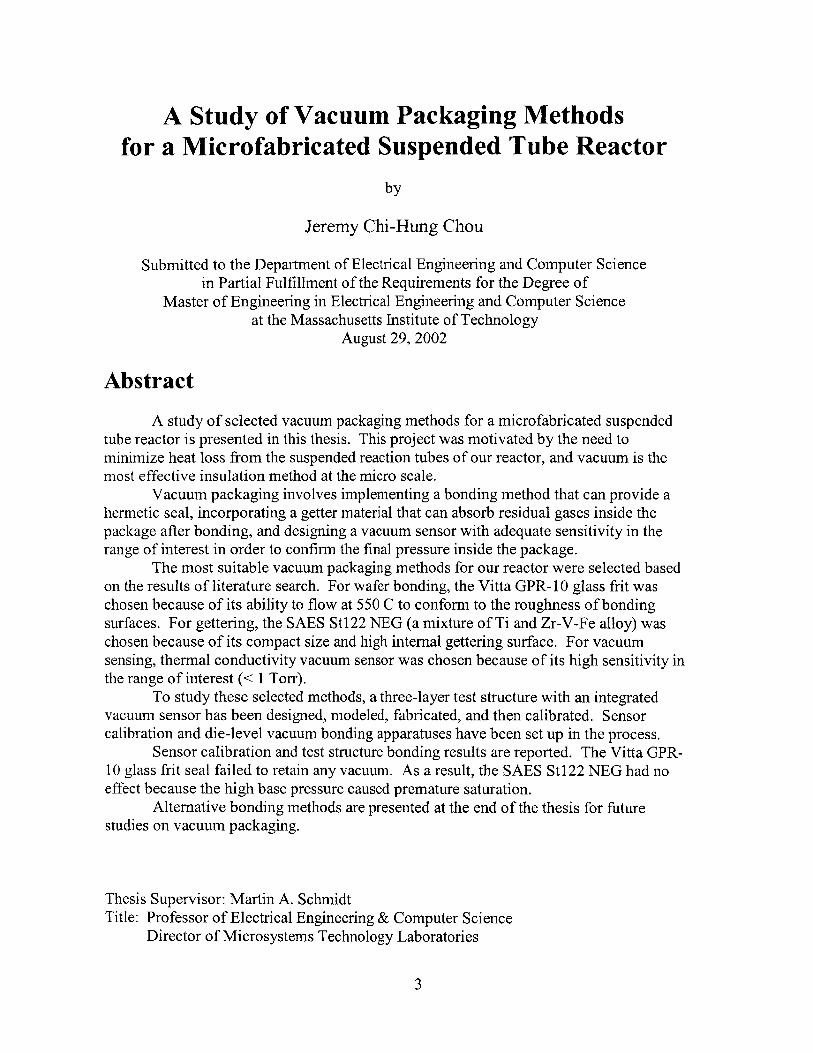
Abstract
A study of selected vacuum packaging methods for a microfabricated suspendedtube reactor is presented in this thesis. This project was motivated by the need tominimize heat loss from the suspended reaction tubes of our reactor, and vacuum is themost effective insulation method at the micro scale.
Vacuum packaging involves implementing a bonding method that can provide ahermetic seal, incorporating a getter material that can absorb residual gases inside thepackage after bonding, and designing a vacuum sensor with adequate sensitivity in therange of interest in order to confirm the final pressure inside the package.
The most suitable vacuum packaging methods for our reactor were selected basedon the results of literature search. For wafer bonding, the Vitta GPR- 10 glass frit waschosen because of its ability to flow at 550 C to conform to the roughness of bondingsurfaces. For gettering, the SAES St122 NEG (a mixture of Ti and Zr-V-Fe alloy) waschosen because of its compact size and high internal gettering surface. For vacuumsensing, thermal conductivity vacuum sensor was chosen because of its high sensitivity inthe range of interest (< 1 Torr).
To study these selected methods, a three-layer test structure with an integratedvacuum sensor has been designed, modeled, fabricated, and then calibrated. Sensorcalibration and die-level vacuum bonding apparatuses have been set up in the process.
Sensor calibration and test structure bonding results are reported. The Vitta GPR-10 glass frit seal failed to retain any vacuum. As a result, the SAES St122 NEG had noeffect because the high base pressure caused premature saturation.
Alternative bonding methods are presented at the end of the thesis for futurestudies on vacuum packaging.
Thesis Supervisor: Martin A. SchmidtTitle: Professor of Electrical Engineering & Computer Science
Director of Microsystems Technology Laboratories
3

4
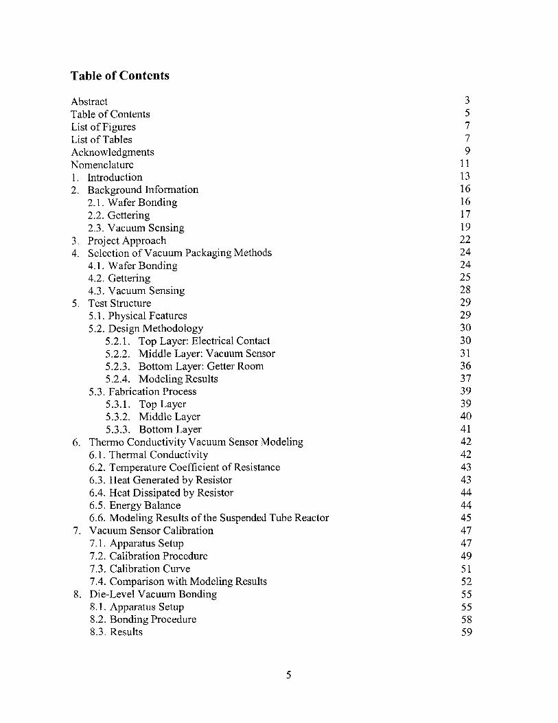
Table of Contents
Abstract 3Table of Contents 5List of Figures 7List of Tables 7Acknowledgments 9Nomenclature 111. Introduction 132. Background Information 16
2.1. Wafer Bonding 162.2. Gettering 172.3. Vacuum Sensing 19
3. Project Approach 224. Selection of Vacuum Packaging Methods 24
4.1. Wafer Bonding 244.2. Gettering 254.3. Vacuum Sensing 28
5. Test Structure 295.1. Physical Features 295.2. Design Methodology 30
5.2.1. Top Layer: Electrical Contact 305.2.2. Middle Layer: Vacuum Sensor 315.2.3. Bottom Layer: Getter Room 365.2.4. Modeling Results 37
5.3. Fabrication Process 395.3.1. Top Layer 395.3.2. Middle Layer 405.3.3. Bottom Layer 41
6. Thermo Conductivity Vacuum Sensor Modeling 426.1. Thermal Conductivity 426.2. Temperature Coefficient of Resistance 436.3. Heat Generated by Resistor 436.4. Heat Dissipated by Resistor 446.5. Energy Balance 446.6. Modeling Results of the Suspended Tube Reactor 45
7. Vacuum Sensor Calibration 477.1. Apparatus Setup 477.2. Calibration Procedure 497.3. Calibration Curve 517.4. Comparison with Modeling Results 52
8. Die-Level Vacuum Bonding 558.1. Apparatus Setup 558.2. Bonding Procedure 588.3. Results 59
5
9. Sensor Resistor Failure Analysis9.1. Description9.2. Possible Causes9.3. Solutions
9.3.1. Tantalum Nitride (TaN) Diffusion Barrier9.3.2. Aluminum Oxide (A120 3) Diffusion Barrier9.3.3. Careful Temperature Control
10. Evaluation of Vacuum Package10.1. Summary10.2. Vacuum Sensor Measurements10.3. Leak Tests10.4. Vacuum Packaging Failure Analysis
11. Future Work12. Conclusion13. ReferencesAppendix A: Vacuum Sensor Modeling on Microsoft ExcelAppendix B: Test Structure Mask Drawings on AutoCADAppendix C: Test Structure Detailed Fabrication Process FlowAppendix D: Equipment ListAppendix E: Molecular Flow CalculationsAppendix F: Experimental Data on the Target Pressure
6
606060626262636464646667707374767882848586
Figure 1:Figure 2:Figure 3:
Figure 4:Figure 5:Figure 6:Figure 7:Figure 8:Figure 9:Figure 10:Figure 11:Figure 12:Figure 13:Figure 14:Figure 15:Figure 16:Figure 17:Figure 18:Figure 19:Figure 20:Figure 21:Figure 22:Figure 23:Figure 24:Figure 25:Figure 26:Figure 27:Figure 28:
Gettering mechanisms for some common gasesPhysical properties of Vitta GPR-10 glass transfer tapePhysical properties of SAES St122 getterParameters of the proposed sensor designModeling parameters of the suspended tube reactorTi/Pt/Ti resistance increase during bondingBonding parameters and vacuum sensor measurementsLeak test results
7
List of Figures
Top and side views of the suspended tube reactorLeaks created by surface roughness in the case of anodic bondingSAES St122 package and its pumping speed as a function of the absorbedquantityCross sectional view of the test structureTop and cross sectional views of the top layerTop, bottom, and cross sectional views of the middle layerThree heat transport modes for the sensor resistorDetailed diagram of the sensor resistorSpecifications of the sensor resistor and the membraneTop and cross sectional views of the bottom LayerModeling results of the proposed sensor designFabrication process for the top layerFabrication process for the middle layerFabrication process for the bottom layerModeling and experimental results for the suspended tube reactorVacuum sensor calibration setupUltra high vacuum chamber and its connectionsFour-point measurement setupGlass frit tape placement on a calibration sampleVacuum sensor calibration curves of three samplesDie-level vacuum bonding setupTop and cross sectional views of the bonding chuckDie-level vacuum bonding setupHeating cycle for the glass frit bondingPlacement of A120 3 diffusion barrier and glass fritVoids in Si-Pyrex glass frit bondVoids in Si-Si glass frit bondPossible implementation of solder bonding on test structure
142427
29303132363637383940414647484951545656575863686971
List of Tables
Table 1:Table 2:Table 3:Table 4:Table 5:Table 6:Table 7:Table 8:
1825273546606566

8

Acknowledgments
I would first like to thank Professor Martin Schmidt and Professor Klavs Jensenfor giving me the opportunity to do this research and for providing constant guidance.
Very important was also the guidance of Leonel Arana, who never hesitated tohelp me in lab and brainstorm with me.
I want to thank Ole Nielson for being a wonderful officemate and for answeringmy research and computer related questions.
Thanks to the other members of the Schmidt and Jensen groups who were alwaysvery supportive: Xue'en, Christine, Becky, Aleks, Cyril, Chelsey, and others.
9

10

Nomenclature
L LengthW WidthH HeightQ PowerA AreaJ Current Density
p ResistivityR Resistance91 Universal Gas ConstantV Voltagek Thermal ConductivityA Mean Free Path
c Mean Free VelocityCVm Constant Volume Molar Heat Capacity
N Molar ConcentrationK Boltzmann ConstantT TemperatureC- Collision Cross Section
M Molar MassP, Transition Pressure
D Distancea Thermal Coefficient of Resistances EmissivityK Stefan-Boltzmann Constant
11

12
1 Introduction
Power is a critical issue for all mobile electronics. While much work is being
done on minimizing the power consumption of circuits, on the power supply side, the
battery has been the only viable technology. Unfortunately, due to the fundamental
constraint on the energy density, battery technology does not seem to be able to keep up
with the power demand of increasingly complex electronics. As a feasible alternative to
the battery, a microfabricated suspended tube reactor has recently been developed in our
group using Micro Electro Mechanical System (MEMS) techniques. This reactor can be
used to produce electricity in different ways. One is to convert a chemical fuel into
hydrogen (e.g. through the ammonia cracking reaction), which can then be fed into a
micro fuel cell to generate electricity. Another is to create heat and light by combusting a
chemical fuel and feed the photons into a photovoltaic cell to generate electricity.'
Our reactor consists of two sets of free standing silicon nitride tubes connected to
one silicon heat exchange zone on one end as shown in Figure 1.1 An exothermic
reaction in one set of tubes can deliver heat through the heat exchange zone to an
endothermic reaction in the other set of tubes (e.g. a hydrogen-generating reaction). In
order to provide a maximum amount of heat to drive the reaction, it is critical to
minimize heat loss to the outside environment. Conductive heat loss occurs in two
modes as shown in Figure 1: one through the silicon nitride tubes, and the other through
the gases in the enclosure. While the heat loss through the tubes is minimized by making
the tube wall as thin as possible (i.e. 2 um), one effective method to prevent the heat loss
through the gases is to create a vacuum space surrounding the hot zone, or in other words,
to create a vacuum package for this reactor. Simply surrounding the tubes with insulation
13

material would not work because at such a small scale, the insulator would add enough
surface area to the tubes to actually increase the heat loss. Based on previous data
(presented in Appendix F), a vacuum of 40 mTorr or less is desirable in order to
minimize heat loss. At 40 mTorr or less, heat loss becomes independent of pressure for
the geometry of our reactor, and achieving a pressure lower than that will not further
decrease heat loss.
r ----- i r ----- Si heat exchange zone
Si slabs for heat recovery
SiN tubes
tube set I tube set 2
heat Conductionthru gaseC
capping chip
he t conduction ~~_~-~~- device chipthru nitride tunis c i h
| V capping chip
Figure 1. Top and side views of the suspended tube reactor, and heat loss modes.
The purpose of this project is to evaluate the feasibility of selected vacuum
packaging methods, including a wafer bonding method that can provide a hermetic seal
over a rough surface in vacuum (i.e. 100 nm thick roughness), a gettering method that can
best absorb residual gases inside the package after bonding, and a vacuum sensing
14

method that can provide adequate sensitivity in the range of interest in order to confirm
the final pressure inside the package. Based on the results of literature search, one wafer
bonding method, one gettering method, and one vacuum sensing method are selected for
investigation. The selection is based on the suitability of each method for our specific
suspended tube reactor. After actually implementing these methods, the feasibility of
each method can be determined.
15
2 Background
2.1 Wafer Bonding
A variety of hermetic wafer bonding methods are available. Anodic bonding is a
method to bond silicon to glass. A voltage of about 1000 V is applied across the silicon
and the glass (with the glass held at the negative potential) while raising the temperature
to 300-500 C. In this condition, the positive Na+ ions in the glass move towards the
cathode and the negative 0- ions move towards the silicon-glass interface. The resulting
electric field pulls the two materials together and forms silicon dioxide at the interface to
make a strong bond.2
Silicon fusion bonding is a method to bond silicon to silicon. Before bonding,
OH groups are attached to the bonding surfaces through a hydration step. Then, they are
brought into contact at a temperature of about 1000 C. Bonding occurs according to the
mechanism: Si-OH + Si-OH - Si-O-Si + H20. No electric field is required.3
Trade-offs exist between these two bonding methods. Anodic bonding requires a
high electrical voltage, which may damage any potential electronics already on the wafer.
Also, the difference between the thermal expansion coefficients of silicon and glass could
result in thermal stress. In contrast, silicon fusion bonding requires no electrical voltage
and has no chance for thermal stress (because no other material is used other than
silicon). However, anodic bonding offers higher tolerance of bonding surface roughness
and requires a lower bonding temperature than silicon fusion bonding.
In addition to anodic bonding and silicon fusion bonding, there are other bonding
methods available that require an intermediate layer as a glue. For example, glass frit
bonding utilizes glass powder suspended in an organic binder. It is first applied onto the
16
bonding surfaces, followed by burning off the binder at about 300 C. Then, they are
pressed together and heated to about 600 C to sinter the glass to form a Si-O-Si bond. No
electric field is required.4
In solder bonding, wettable metal pads need to be first deposited over the non-
wettable silicon surface. This wettable metal usually comprises three layers: an adhesion
metal (e.g. chromium or titanium), a barrier metal (e.g. copper or platinum), and a
sacrificial metal (e.g. gold). The barrier metal is required to prevent the solder from
dissolving the adhesion metal. Then, solder (e.g. tin/lead, indium, gold) is deposited over
the wettable metal. After contacting the two surfaces and heating to the melting point of
the solder (i.e. 250-350 C), the solder begins to flow and bonds the two surfaces.5
Eutectic bonding typically utilizes gold as a glue layer. As the temperature rises,
gold gradually diffuses into silicon. When the eutectic composition is reached (97%
silicon and 3% gold), the melting point of the silicon-gold system decreases to the
minimum value of 363 C. At this temperature, liquid alloy of silicon-gold forms and
bonds the two surfaces.4
Thermal compression bonding also relies on gold as a glue layer. In this case,
gold is deposited onto each of the two surfaces with titanium as an adhesion layer. The
two gold surfaces are then brought into contact while applying about 20 psi pressure and
heating to about 300 C (this temperature even lower than the eutectic temperature).
Bonding occurs between the two gold layers. 3
2.2 Gettering
Getters are highly reactive metals or metal alloys that chemically react with gas
molecules and pump away the products by adsorption and/or absorption. These gas
17

molecules may have originated from the silicon surface and from the bonding process.
Because getters work by chemical reaction, they are unable to remove inert gases (e.g.
He, Ne, and Ar).6
Getters provide a clean surface for the gas molecules to collide on. After
collision, gas molecules stick on the surface, react with the getter, and then either remain
on the getter surface or diffuse into the getter bulk. The gettering mechanisms for some
of the common gases are shown in Table 1 .6
Table 1. Gettering mechanisms for some common gases. (g) stands for the gaseous state,and (a) stands for the adsorbed state. G stands for getter.
Gas Reaction MechanismCO CO (g) 4 CO (a) + G 4 G-C + G-OC02 CO2 (g) - CO (a) + G - G-C + 2 G-ON2 N2 (g) 4 N2 (a) + G + 2 G-NNO NO (g) 4 NO (a) + G 4 G-O + G-NH2 H2 (g) 4 2 H (a) 4 2 H (bulk)
H20 H20 (g) 4 2 H (a) + G-O+ 2 H (bulk) + G-O
There are two ways to create clean getter surface. In the case of evaporable
getters, the getter is evaporated and a thin layer is deposited on the inner surface of an
enclosure. Another thin layer is to be deposited periodically to replenish the clean
surface. In the case of non-evaporable getters, instead of relying on the inner surface of
an enclosure, the getter has a porous internal structure to provide the reaction surface.
Heat induces the adsorbed gas molecules on the surface to diffuse into the getter bulk to
leave the surface clean.7
One common evaporable getter is titanium due to its high reactivity with many
gases. It evaporates at about 1500 C. Due to its high reactivity, the titanium getter can
18

only operate in a vacuum of 10-3 Torr or less. If it is exposed in atmosphere, it will
quickly oxidize and lose its gettering capability. 6
Non-evaporable getters (NEG) are mostly metal alloys (e.g. Zr(84%)-Al(12%)
and Zr(70%)-Al(25%)-Fe(5%)). They have high porosity (50-70%) so they can rely on
their own internal surface area for reaction. In order to activate the getter, it needs to be
heated to 500-800 C so an oxide passivation layer on the surface can diffuse into the
bulk. NEGs prefer to operate in a heated environment because heat helps the adsorbed
gas molecules to diffuse into the bulk and free up the surface; however, they can still
work at room temperature with a lower gettering speed. As the getter becomes saturated,
its gettering speed decreases accordingly. When the pumping capacity is eventually
reached, the whole getter will need to be replaced.6
2.3 Vacuum Sensing
Once the suspended tube reactor is packaged in vacuum, it is important to
accurately measure the pressure inside the package in order to confirm the achieved
vacuum and to monitor for leaks and outgassing. Many vacuum sensing methods are
available. The simplest method is to create a membrane on the package and optically
measure its deflection, which is directly proportional to the pressure difference across the
membrane. The amount of deflection follows Equation 1:
W = P(a 2 - r2)2 , where D = Et3 Equation 164D 12(1 - v2
where W is the amount of deflection, P is the pressure load, a is the radius of membrane,
r is the radial distance from center of membrane, D is the flexural rigidity of the
membrane, E is the elastic modulus, and v is the Poisson's ratio.8 When the membrane
19
deflection is zero, the pressure inside the package equals the pressure outside the
package. Adjusting the external pressure until the membrane becomes flat is a simple
method to know the pressure inside.
In the capacitive method, two metal plates are placed close to each other, one
fixed and the other on a flexible membrane. The capacitance between the two plates is
inversely proportional to the distance between them, which in turn depends on the
deflection of the membrane, which in turn depends on the pressure difference across the
membrane. Therefore, capacitance corresponds to pressure. Capacitance measurement
can be more accurate than the optical measurement of membrane deflection.9
The basic setup of a thermal conductivity vacuum sensor consists of a resistor
placed on a membrane inside an enclosure. The resistor generates heat when a voltage is
applied across it. The balancing heat loss from the resistor occurs in three modes:
conduction through the gases in the enclosure, conduction through the membrane which
the resistor is sitting on, and radiation. While the latter two modes are independent of the
pressure, heat conduction through the gases is directly proportional to the thermal
conductivity of the gases, which is in turn directly proportional to the pressure within a
certain pressure range. Thermal conductivity does not become dependent on the pressure
until the mean free path of the gas molecules becomes limited by the geometry of the
enclosure housing the resistor.10
A thermal conductivity vacuum sensor can measure in two ways. In the constant
voltage mode, the pressure can be determined by measuring the resistance when a
constant voltage is applied across the resistor. The relationship between the pressure and
the resistance is that an increase in pressure will increase the thermal conductivity, which
20

will in turn increase the heat loss from the resistor, which will in turn decrease the
temperature of the resistor, which will in turn decrease its resistance. In the constant
temperature mode, the pressure can be determined by measuring the amount of power
required to maintain the resistor at a constant temperature. The relationship between the
pressure and the power is that an increase in pressure will increase the heat loss from the
resistor, which will in turn increase the power necessary to maintain the given
temperature.
21

3 Project Approach
This project investigates the feasibility of selected vacuum packaging methods. It
focuses on three components of vacuum packaging. The first is an effective wafer
bonding method. In order to create an enclosed package, the suspended tube reactor
needs to be bonded to a layer on the top and a layer on the bottom. Furthermore, in order
to have vacuum inside the package, this bonding process needs to take place in vacuum
and the resulting bond needs to be hermetic to prevent air leak after it is taken out of the
vacuum environment. The second component is an effective getter material. A getter
helps maintain a low pressure by pumping away the residual gases in the package through
chemical reaction. Getters may not always be required for vacuum packaging. However,
for the micro-scale MEMS devices where the surface-to-volume ratio is relatively high,
such as our suspended tube reactor, a getter is usually required to counter the outgassing
from the internal surface of the package. The third is an effective vacuum sensor which
has an adequate sensitivity in the targeted pressure range of the package. A vacuum
sensor is not necessarily required in the actual finished package; however, in the process
of creating such a package, it is needed to confirm the achieved vacuum level.
The first part of the project is to select the most suitable wafer bonding, gettering,
and pressure sensing methods for our reactor through literature search. The factors being
considered in these selections are presented in Section 4. The goal is to evaluate the
vacuum package achieved by using these selected methods.
The second part of the project, presented in Section 5, is to design and fabricate a
test structure to experiment with these selected vacuum packaging methods. The actual
suspended tube reactor can not be used for this project because its supply is very limited
22
due to its complicated fabrication process. This simpler test structure basically includes a
vacuum sensor (to test the selected vacuum sensing method), a getter room (to test the
selected getter material), and a bonding surface topography similar to that of a real
suspended tube reactor (to test the selected wafer bonding method). The assumption is
that if this test structure can achieve a vacuum package, then the same methods can be
transferred to a real suspended tube reactor.
The third part of this project, presented in Section 6, is to model the thermal
conductivity vacuum sensor. This model, based on an energy balance between the heat
generated and the heat lost from the sensor resistor, helps design a sensor that has
adequate sensitivity between 0 and 1 Torr, the targeted pressure range of the package.
The fourth part of the project, presented in Section 7, is to calibrate the vacuum
sensor and compare the experimental results to the modeling results. The resulting
calibration curve is relied upon when the sensor is later used to determine the vacuum
level inside the package.
The fifth part of the project, presented in Section 8, is to perform die-level
vacuum bonding experiments and to evaluate the effectiveness of the package.
Finally, the last part of the project, presented in Section 9, 10, and 11, is to
analyze and evaluate the selected vacuum packaging methods and to suggest improved
techniques for future studies.
23

4 Vacuum Packaging Method Selection
4.1 Wafer Bonding
The suspended tube reactor has 400 nm thick platinum resistors on the top
surface. This poses a challenge to achieving a hermetic seal because it is difficult to seal
the area where the edge of the resistor meets the substrate as shown in Figure 2 in the
case of anodic bonding. Anodic bonding and silicon fusion bonding will not work
because of their low tolerance of surface roughness (about 50 nm and 6 nm,
respectively).3 Eutectic bonding and thermal compression bonding are possible
candidates, but they also require a very flat bonding surface. Glass frit bonding has a
much higher tolerance for surface roughness due to its flow characteristic. At the melting
temperature of the glass, softened glass can flow everywhere and conform to the surface
topography. Gooch has achieved 9 mTorr pressure with glass frit bonding." Solder has
the same flow characteristic as glass frit at its melting temperature; however, solder is
electrically conductive while glass frit is insulating, so special care needs to be taken to
prevent the solder from short-circuiting the platinum resistor
leaks
pyrex glassmetal
Si substrate
Figure 2. Leaks created by surface roughness in the case of anodic bonding.
24
The glass frit material chosen for this project is the GPR-10 Glass Transfer Tape
manufactured by Vitta Corporation. This glass frit comes in the form of a tape with one
adhesive side. It is specifically designed for glazing and sealing silicon wafers. It may
also be used for glazing, sealing, and joining other materials having a coefficient of
expansion of approximately 6.5 x 10⁻⁶. GPR-10 is a lead-zinc-borosilicate type glass
thermally matched to silicon so that the fired coatings do not have stress or cracks. The
thickness of the tape is 25 um before sintering and 40 um after sintering. This increase in
thickness (and volume) is caused by the expansion of the organic binder as it is heated up
and evaporates from the interior of the glass frit during sintering. The increased volume
is believed to be made up of voids. Physical properties are summarized in Table 2.
Table 2. Physical properties of Vitta GPR-10 glass transfer tape.Glass Family Lead-Zinc-BorosilicateGlass Type VitreousAnnealing Point ~ 425 CSoftening Point ~510 CWorking Temperature 552 - 600 CCoefficient of Thermal Expansion 6.5 x 10⁻⁶ in/in CDielectric Constant, 1 megacycle, 25 C 12
4.2 Gettering
Non-evaporable getters (NEG) have many advantages over evaporable getters,
especially when applied in the MEMS devices.6, 7 Their porous structure supplies their
own reactive surface instead of relying on an external surface, which a MEMS device
usually does not have much of. NEGs obtain clean surface by making the adsorbed
molecules diffuse into the bulk instead of by the rather troublesome evaporation process
in the case of evaporable getters. The absence of evaporation also means a lower
25

operating temperature. A mixture of titanium (Ti) and zirconium (Zr)-vanadium (V)-iron
(Fe) alloy is popular due to its low activation temperature of about 450 C. Esashi has
achieved a vacuum level of 105 Torr with Ti and Zr-V-Fe. 1 2
The getter chosen for this project is St122 manufactured by SAES Corporation, a
mixture of Ti and Zr-V-Fe. A key goal in the development of St122 was flexible
manufacture. Strips may be produced as either single or double coated and can be
designed to fit in constrained volumes. Possible substrate materials include nichrome,
nicrofer, titanium, nickel, moly, stainless steel, and zirconium. A process involving
screen printing and sintering of the getter material results in a high-porosity, low-
particulating, and mechanically strong structure. Successful application in MEMS
applications requires a good activation of the getter to maximize use of the available
active mass. Typical processes would consist of prebaking the package before bonding in
order to reduce the amount of gases present on the surface that could outgas. When the
package is ready for final sealing the getter should be activated first in order to gain
maximum performance before sealing. The getter activation process consists of
supplying enough heat energy for the protective passivation layer on the outer surface to
diffuse into the bulk, thereby exposing chemically active getter alloy. This process is
typically 10 minutes at 450 C to 500 C. Physical properties of St122 are summarized in
Table 3. Like all other NEGs, the pumping speed of St122 is a function of the type of gas
and the amount already absorbed as shown in Figure 3.
26
Table 3. Physical properties of SAES St122 getter.
Emissivity 0.6-0.65
Density 4.7 g/cm 3
Apparent Density 2 g/cm3 (due to high porosity 55%-65%)
Mass of Getter Material 20 mg/cm2 for a 1 00um thick layer
Thermal Properties N/A
Figure 3. SAES St122 package (with six 1 mm x 1 mm pellets shown in picture) and its
pumping speed as a function of the absorbed quantity.
27
Pumping Speed Vs. Sorbed Quantity
EIC
U
10
10 -Coating Thickness: 100 um
E Sorption Temperature: 25 CSorption Pressure: 3e-5 Torr
0.01 0.1 1 10 100
Sorbed Quantity (cc.torr/cm2 of getter coating)

4.3 Vacuum Sensing
Both the optical method and the capacitive method rely on the deflection of a thin
silicon membrane caused by the pressure difference across it. One problem with this
approach is that even when the pressure difference across the membrane is zero, there
may still be some membrane deflection due to residual stress, and it is difficult to
quantify the residual deflection. In addition, these membrane-based methods have a poor
sensitivity in a vacuum of 1 Torr or lower because such a small change in pressure can
not cause enough membrane deflection to be detected.
A thermal conductivity vacuum sensor seems the most appropriate for this
project. The actual suspended tube reactor has resistors over the bonding surface. In
order to allow the test structure to accurately simulate the bonding surface of the reactor,
it is a good idea to have the same resistors on the bonding surface of the test structure as
well. This consideration naturally leads to a sensor based on thermal conductivity
because it would also need to have resistors. In addition, such a sensor has been shown
to have good sensitivity below 1 Torr, which is the targeted range of this project.
28

5 Test Structure
5.1 Physical Features
The three-silicon-layer test structure, whose cross section is shown in Figure 4, is
a vehicle on which bonding experiments are carried out in this project. Its outer
dimensions are 10 mm (L) x 8 mm (W) x 1.5 mm (H). The top layer includes four
electrical contact holes to the resistor and a cavity in which the pressure is measured.
The middle layer contains two cavities etched from the backside in potassium hydroxide
(KOH): one is used to release a stoichiometric silicon nitride (Si 3N4) membrane and the
other is used to equilibrate the pressures across the membrane. A three-layer metal
structure, comprised of titanium-platinum-titanium on the first generation devices and
tantalum-platinum-tantalum on the second generation devices, sits on top of the
membrane and serves as the heating resistor of the vacuum sensor. The bottom layer
includes a deep cavity for placing the getters.
electricalcontact heating resistor
Si
Si3N4
Si glass frit
getter room
Si3N4 membrane pressure equilibration hole
Figure 4. Cross sectional view of the test structure.
29
5.2 Design Methodology
5.2.1 Top Layer: Electrical Contact
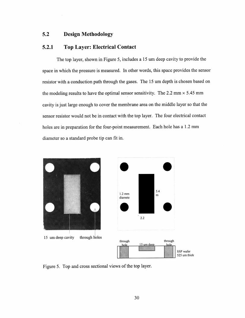
The top layer, shown in Figure 5, includes a 15 um deep cavity to provide the
space in which the pressure is measured. In other words, this space provides the sensor
resistor with a conduction path through the gases. The 15 um depth is chosen based on
the modeling results to have the optimal sensor sensitivity. The 2.2 mm x 5.45 mm
cavity is just large enough to cover the membrane area on the middle layer so that the
sensor resistor would not be in contact with the top layer. The four electrical contact
holes are in preparation for the four-point measurement. Each hole has a 1.2 mm
diameter so a standard probe tip can fit in.
1.2 mm mdiamete
2.2
15 urn deep cavity through holesthrough through
TI~u~e~TJT SSP wafer
525 urn thick
Figure 5. Top and cross sectional views of the top layer.
30

5.2.2 Middle Layer: Vacuum Sensor
The middle layer, whose top view is shown in Figure 6 , includes the heating
resistor of the vacuum sensor. Four contact pads are placed in the far corners to
maximize the area of flat surface for bonding.
1.4 mm
1.8 mn contactpad
resistor
KOH etchedthrough holes
contactpad
contactpad
DSP wafer450 urn thick
Figure 6. Top, bottom, and cross sectional views of the middle layer.
31
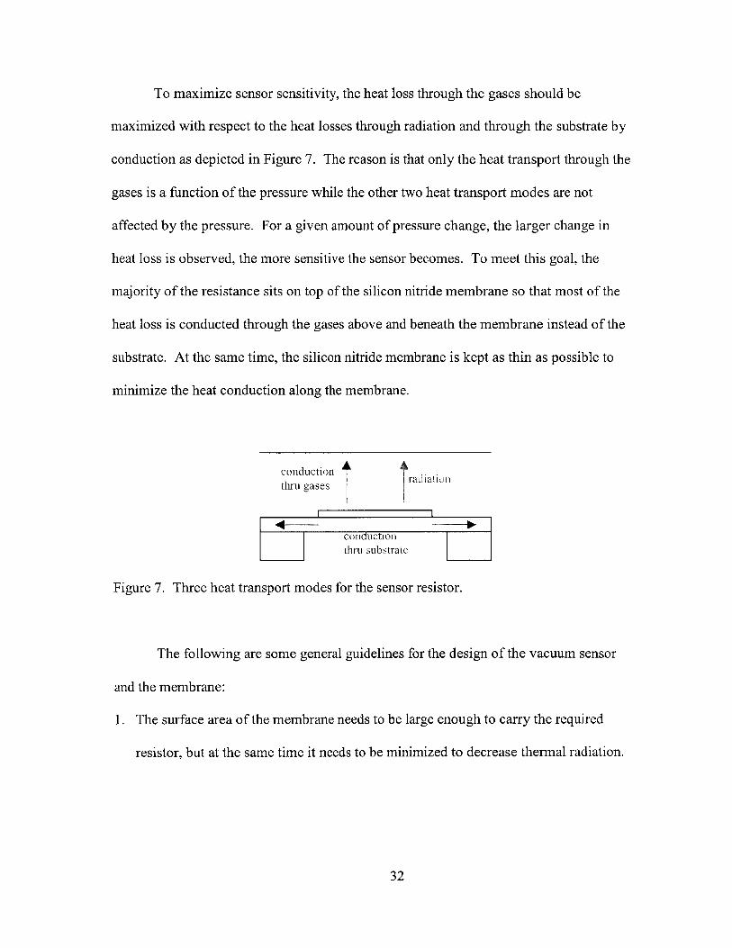
To maximize sensor sensitivity, the heat loss through the gases should be
maximized with respect to the heat losses through radiation and through the substrate by
conduction as depicted in Figure 7. The reason is that only the heat transport through the
gases is a function of the pressure while the other two heat transport modes are not
affected by the pressure. For a given amount of pressure change, the larger change in
heat loss is observed, the more sensitive the sensor becomes. To meet this goal, the
majority of the resistance sits on top of the silicon nitride membrane so that most of the
heat loss is conducted through the gases above and beneath the membrane instead of the
substrate. At the same time, the silicon nitride membrane is kept as thin as possible to
minimize the heat conduction along the membrane.
conduction Oniaif
thru. gases
conductionthru substrate
Figure 7. Three heat transport modes for the sensor resistor.
The following are some general guidelines for the design of the vacuum sensor
and the membrane:
1. The surface area of the membrane needs to be large enough to carry the required
resistor, but at the same time it needs to be minimized to decrease thermal radiation.
32
2. While maintaining the structural integrity of the membrane, the thickness and the area
of the membrane should be minimized and maximized, respectively, in order to
minimize the heat transport along the membrane.
3. The distance between the resistor and the top enclosure wall needs to be minimized in
order to maximize heat transport through the gases given the constraint that the
resistor can not be in contact with the wall.
4. The applied voltage and the base resistance dictate the current and the temperature of
the resistor. The current needs to be high enough to be accurately measured but not
higher than what the electron migration limit allows. Also, the resistor temperature
should remain low to minimize the radiation effects.
5. The resistance of the metal leading to the membrane from the contact pads should be
minimized. It is important to keep as much of the resistance on the membrane as
possible.
6. It is important to perform four-point measurement to minimize the noise effect of the
contact resistance of the pad and the probe. Therefore, four contact pads and four
wires leading to the membrane are required.
7. The resistor material should be chosen to have a large and linear Temperature
Coefficient of Resistance (TCR).
The specifications of the proposed vacuum sensor design are summarized in
Table 4 and graphically presented in Figure 8 and Figure 9. The composition and the
thickness of the resistor on the test structure are set be identical to those of the resistor on
the actual suspended tube reactor. The resistor composition is Ti (10 nm)/Pt (100 nm)/Ti
(10 nm) on the first generation devices, and Ta (10 nm)/Pt (400 nm)/Ta (20 nm) on the
33

second generation devices. The reason for this change is that the Ta/Pt/Ta structure
provides a much longer resistor lifetime at high temperatures (i.e. -1000 C). The vacuum
sensor design presented in this section is based on the Ti/Pt/Ti resistor structure. The
second generation vacuum sensor has the identical design except for the thickness of the
resistor. The width of the resistor is set to be 100 um to balance between
manufacturability and the membrane size. An increase in the metal line width will make
it easier to fabricate but will make the membrane area larger and thus easier to break.
The current density of the resistor is set to be 2 x 10⁹ A/m 2 while the electron migration
limit of platinum is 1010 A/m 2 . Power generated at room temperature is set to be 0.05 W
to balance between the resistor length and the signal power. When more power is
generated, the sensor signal becomes stronger, but the resistor must become longer to
maintain the pre-determined current density and thus more prone to fracture. Length is
calculated to be 11.8 mm from Equation 2:
L = Q EquatiorWHJ 2 p
where L, W, and H are the length, width, and thickness of the resistor, Q is the power
generated by the resistor, J is the current density through the resistor, and p is the
resistivity of platinum. The resistance is calculated to be 125 ohm from Equation 3:
R= PL EquatiorWT
The amount of voltage must applied is calculated to be 2.5 V from Equation 4:
V = RE Equation 4
The length of conduction through the membrane is set to be 100 um to balance between
the undesirable heat transport and membrane size. When this length increases, the heat
34
2
3
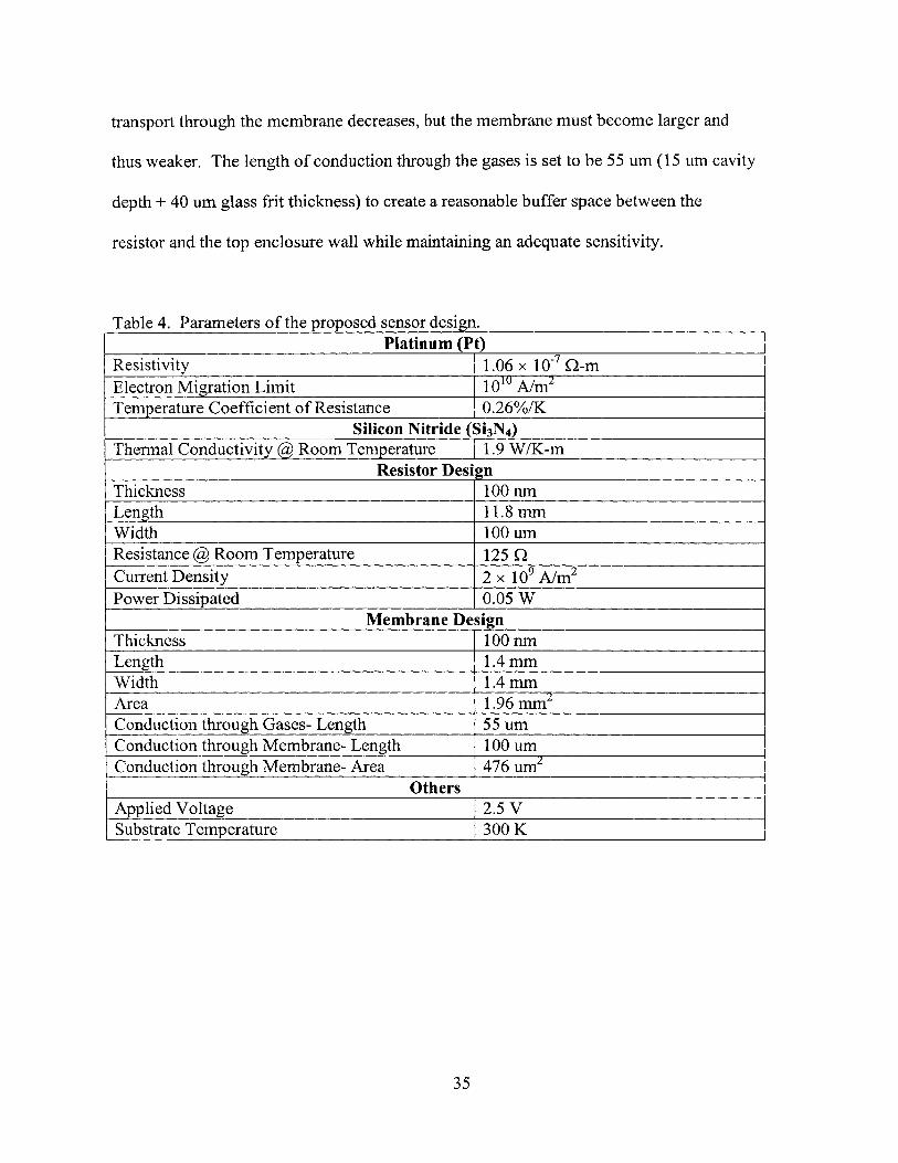
transport through the membrane decreases, but the membrane must become larger and
thus weaker. The length of conduction through the gases is set to be 55 um (15 um cavity
depth + 40 urn glass frit thickness) to create a reasonable buffer space between the
resistor and the top enclosure wall while maintaining an adequate sensitivity.
Table 4. Parameters of the proposed sensor design.Platinum (Pt)
Resistivity 1.06 x 10~7 Q-mElectron Migration Limit 1010 A/m2
Temperature Coefficient of Resistance 0.26%/KSilicon Nitride (Si 3N4)
Thermal Conductivity @ Room Temperature 11.9 W/K-mResistor Design
Thickness 100 nmLength 11.8 mmWidth 100 umResistance @ Room Temperature 125 QCurrent Density 2 x 10 9 Aim2
Power Dissipated 0.05 WMembrane Design
Thickness 100 nmLength 1.4 mmWidth 1.4 mmArea 1.96 mm2
Conduction through Gases- Length 55 umConduction through Membrane- Length 100 urnConduction through Membrane- Area 476 um 2
OthersApplied Voltage 2.5 VSubstrate Temperature 300 K
35
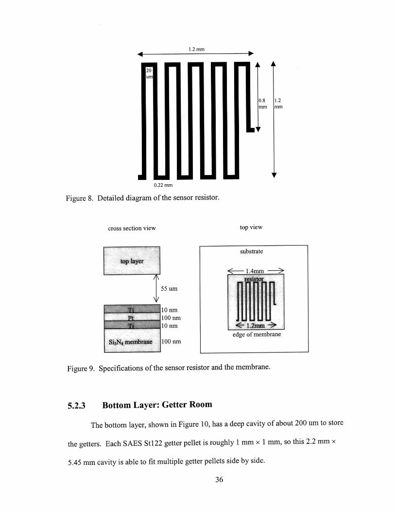
1.2 mm
20U
0.8 1.2mm mm
0.22 mm
Figure 8. Detailed diagram of the sensor resistor.
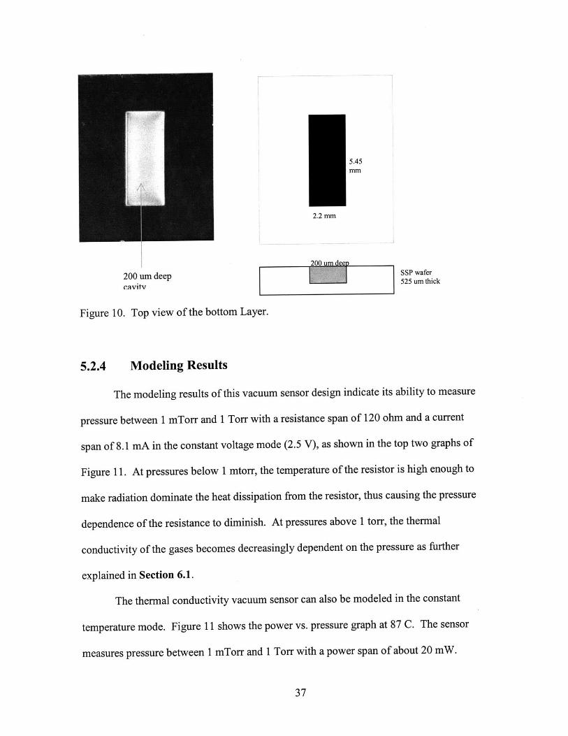
cross section view top view
substrate
< 1.4mm >
55 um
100 nm100 nm
edge of membraneSiN 4 Menirase 100 n
Figure 9. Specifications of the sensor resistor and the membrane.
5.2.3 Bottom Layer: Getter Room
The bottom layer, shown in Figure 10, has a deep cavity of about 200 um to store
the getters. Each SAES St122 getter pellet is roughly 1 mm x 1 mm, so this 2.2 mm x
5.45 mm cavity is able to fit multiple getter pellets side by side.
36
2.2 mm
200 umn deen
200 urn deep SSP wafer
2 0 0 u m d5 2 5 u rn th ic k
Figure 10. Top view of the bottom Layer.
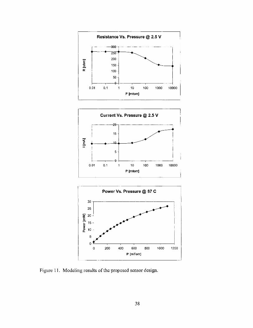
5.2.4 Modeling Results
The modeling results of this vacuum sensor design indicate its ability to measure
pressure between 1 mTorr and 1 Torr with a resistance span of 120 ohm and a current
span of 8.1 mA in the constant voltage mode (2.5 V), as shown in the top two graphs of
Figure 11. At pressures below 1 mtorr, the temperature of the resistor is high enough to
make radiation dominate the heat dissipation from the resistor, thus causing the pressure
dependence of the resistance to diminish. At pressures above 1 torr, the thermal
conductivity of the gases becomes decreasingly dependent on the pressure as further
explained in Section 6.1.
The thermal conductivity vacuum sensor can also be modeled in the constant
temperature mode. Figure 11 shows the power vs. pressure graph at 87 C. The sensor
measures pressure between 1 mTorr and 1 Torr with a power span of about 20 mW.
37
Resistance Vs. Pressure @ 2.5 V
Figure 11. Modeling results of the proposed sensor design.
38
200 -
150 -
100-
50 -
0
0.01 0.1 1 10 100 1000 10000
P [mtorr]
15 -
5-
Current Vs. Pressure @ 2.5 V
0.01 0.1 1 10 100 1000 10000
P [mtorr]
Power Vs. Pressure @ 87 C
30 - - - - - - -
25-
20 -E
15-
10 -
5-
00 200 400 600 800 1000 1200
P [mTorr]
.......... I ....... I ....... .... ........... ..
5.3
5.3.1
Fabrication Process
Top Layer
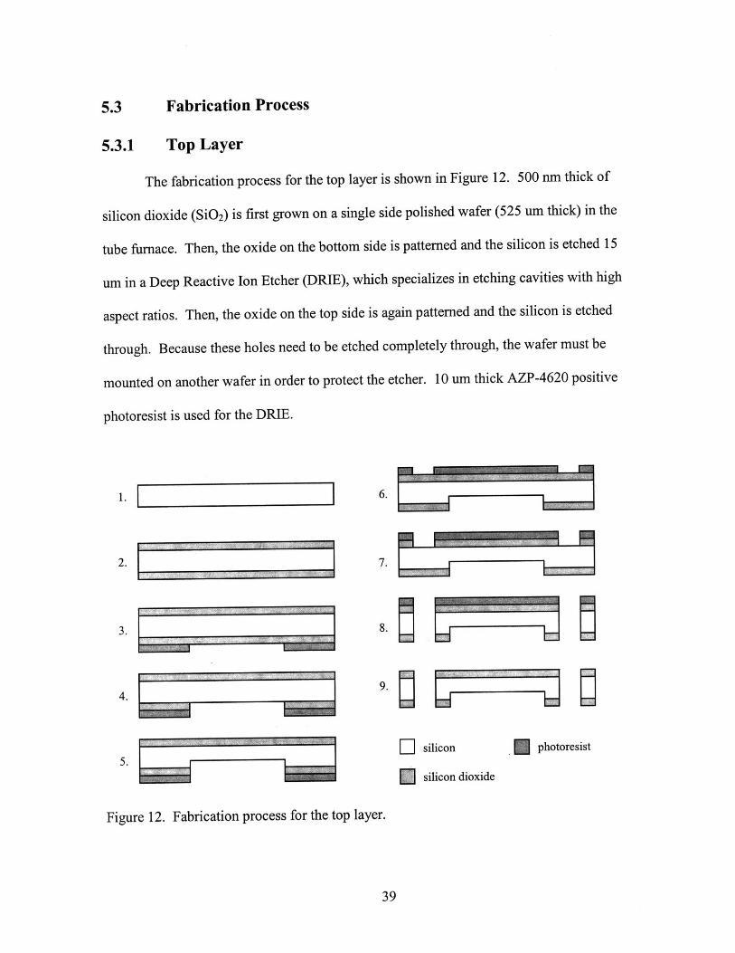
The fabrication process for the top layer is shown in Figure 12. 500 nm thick of
silicon dioxide (SiO2) is first grown on a single side polished wafer (525 um thick) in the
tube furnace. Then, the oxide on the bottom side is patterned and the silicon is etched 15
um in a Deep Reactive Ion Etcher (DRIE), which specializes in etching cavities with high
aspect ratios. Then, the oxide on the top side is again patterned and the silicon is etched
through. Because these holes need to be etched completely through, the wafer must be
mounted on another wafer in order to protect the etcher. 10 um thick AZP-4620 positive
photoresist is used for the DRIE.
am amaummm am
77 1 77
6.
7.
8.
9.
D silicon
silicon dioxide
photoresist
Figure 12. Fabrication process for the top layer.
39
1.
2.
3.
4.
5.
5.3.2 Middle Layer
The fabrication process for the middle layer is shown in Figure 13. 100 nm thick
stoichiometric silicon nitride (Si 3N4) is first deposited on a 450 nm thick double side
polished wafer. Then, the nitride on the bottom side is patterned with 1 um thick OCG-
825 positive photoresist and etched through in a RF magnetically coupled etcher. Then,
the nitride on the top side is patterned for metal deposition. 10 nm Ti/100 nm Pt/10 nm
Ti (first generation) or 10 nm Ta/400 nm Pt/20 nm Ta (second generation) is deposited on
the wafer. The unwanted metal is then removed in a lift-off process. 1.5 um thick
negative image reversal photoresist is used for the lift-off process. Finally, the cavities
are etched through from the back side, stopping on the nitride layer, in 20% KOH
solution at 80 C. Because KOH attacks Pt easily, the front side of the wafer is protected
in a sealed chuck while the back side is being etched.
I I 5.
6.
7.
D silicon * silicon nitride
Figure 13. Fabrication process for the middle
8.
h r11metal photoresist
laye
40
1.
2.
3.
4.
* as 7 .. 1.ann
r.
5.3.3 Bottom Layer
The fabrication process for the bottom layer is shown in Figure 14. 500 nm thick
silicon dioxide (SiO 2) is first grown on a 525 um thick single side polished wafer in the
tube furnace. Then, the oxide on the top side is patterned and the silicon is etched 200
um in the DRIE.
1.
2.
3.
4.
5.
6.
E] silicon E silicon dioxide
Figure 14. Fabrication process for the bottom layer.
photoresist
41
Lj~ IS=
5170 =17
77T,
Thermal Conductivity Vacuum Sensor Modeling
Thermal Conductivity
The thermal conductivity of a gas can be expressed as
1 -k = 3 A c C,, N
3Equation 5
where A, c, Cv,, , and N are the mean free path, the mean velocity, the constant-
volume molar heat capacity, and the molar concentration of the gas molecules,
respectively. 13 The mean free path can be expressed as
A = Equation 6
where K is the Boltzmann constant (1.381 x 10⁻²³ J/K), and T , a, P are the
temperature, the collision cross section, and the pressure of the gas molecules,
respectively.13 The mean velocity can be expressed as
- 891T Equation 7;TM
where 91 is the universal gas constant (8.3145 J/K-mol) and M is the molar mass of the
gas molecules.1 3 The molar concentration can be expressed as
Equation 8N =91T
As a result, the overall expression for the thermal conductivity is
k 5 K91T Equation 93V V - M
At high pressures, the thermal conductivity is independent of the pressure as
shown in Equation 9 because the pressure terms in the mean free path expression and the
42
6
6.1
molar concentration expression cancel each other. However, as the pressure decreases,
the mean free path will increase until it eventually becomes limited by the geometry of
the enclosure. The transition pressure at which this phenomenon occurs can be expressed
as
P =KT Equation 10
where D is the geometry size (i.e. the distance between the resistor and the enclosure
wall). 13 As the pressure decreases past P, the mean free path gradually reaches the
saturation value D , and the thermal conductivity gradually becomes dependent on the
pressure. To model this pressure dependence, the thermal conductivity is expressed as' 4
1+P
Equation 11
6.2 Temperature Coefficient of Resistance
The resistance value of a resistor is directly proportional to the temperature. The
relationship can be expressed as
R R = a(T - T') Equation 12
where a is a material property called the temperature coefficient of resistance (TCR).1 5
A high a value is desirable because it helps achieve better sensor sensitivity. For
example, platinum has a TCR of 0.26%/K.1 5
6.3 Heat Generation by Resistor
When a voltage is applied across a resistor, the amount of energy generated can
be expressed as
43
Equation 13
Heat Dissipation from Resistor
Heat transport by conduction is governed by the Fourier Law:
S . = kAT - ToQConduction r L
Equation 14
where k is the thermal conductivity of the medium, T,. is the resistor temperature, T is
the ambient temperature at the wall, and A and L are the area and the length of the
conduction path (i.e. the path between the resistor and the wall), respectively. 16
Heat transport by radiation follows the equation
QRadiation ~ KA(T 4 _T4) Equation 15
where e is the emissivity of the material, and K is the Stefan-Boltzmann constant (5.67
x 10-8 W/m 2 _K 4). 16
6.5 Energy Balance
The model is based on the following energy balance:
QGeneration C Qconduction-gases + QConduction-membrane + QRadiation Equation 16
Heat conduction takes two paths: one through the gases in the enclosure (Qconduction-gases),
and the other through the membrane (QConduction-membrane). Heat radiation comes from only
the heated resistor (QRadiation). Expanding out each of the Q terms, the energy balance
becomes:
v2 T -T T - T-- = kairA m, +kmAe, + CmemKAm(T,- Tr 4)R Lmem-cs Lmem
Equation 17
44
6.4
QGenerationV 2
R

where Ame, is the membrane surface area, Amem-cs is the membrane cross sectional area, k
is the thermal conductivity, T, is the resistor temperature, T, is the ambient temperature,
Leavity is the distance from the resistor to the wall, Lmem is the distance from the resistor to
the edge of the membrane, e,,, is the membrane emissivity, and K is the Stefan-
Boltzmann constant.
This model makes the following assumptions:
1. Heat conduction and radiation are one-dimensional.
2. Air has a constant thermal conductivity independent of the temperature (neglecting
the temperature gradient between the resistor and the wall).
3. Heat convection is negligible because air is relatively stationary inside the enclosure.
4. The membrane is isothermal and has the same temperature as the resistor itself.
5. The enclosure wall is at room temperature.
6.6 Modeling Results for the Suspended Tube Reactor
The resistance vs. pressure relationship of the actual suspended tube reactor is
generated by this model and compared with previous experimental data in order to verify
the accuracy of the model. The suspended tube reactor has free-standing silicon nitride
tubes with resistors sitting on top of them. These resistors are used to heat up the
reactants inside the tubes in order to initiate a chemical reaction. Therefore, the reactor
itself can function as a thermal conductivity vacuum sensor. This model generated a
resistance vs. pressure graph at a constant voltage input of 10 V, shown in Figure 15,
based on the parameters of the reactor summarized in Table 5. The modeling results do
not exactly agree with the previously collected experimental data,I which show that the
resistance reaches a maximum value of 2400 ohm at 40 mTorr. The modeling results
45
show that the resistance reaches a maximum value of 1700 ohm at 1 mTorr. The
discrepancies are likely the result of the assumptions made in the model, explained in
Section 6.5, and the approximations of the geometries of the heat conduction and
radiation paths, presented in Table 5.
Table 5. Modeling parameters of the suspended tube reactor.RO of Resistor 900 QTCR of Platinum 0.26%/KThermal Conductivity of SiN @ Room Temperature 1.9 W/K-mApplied Voltage lOVSubstrate Temperature 300 KSurface Area of Resistor 6.03 mm 2
Cross Sectional Area of SiN tubes 9536 um2
Conduction Length through Gases 1 mmConduction Length trough SiN Tubes 3020 um
Figure 15. Modeling and experimental results for the suspended tube reactor.
46
Resistance Vs. Pressure @ Constant 10 V
2.62.4 - ..
2.2
- 2.00 1.8
1.6
1.4
1.2
1.0
1.E-06 1.E-04 1.E-02 1.E+00
- exp -+- model Pressure rorr]
Vacuum Sensor Calibration
7.1 Apparatus Setup
The calibration apparatus is shown in Figure 16 and Figure 17. A turbo pump in
series with a mechanical roughing pump (Leybold Trivac B D25B) is used to pump down
the ultra high vacuum chamber. A pressure gauge (KJL-205 Thermocouple Controller
with KJL-6000 Thermocouple Tube) and a gas flow valve are connected to the
feedthroughs. The sample being calibrated is placed into the chamber through a
feedthrough on a loader. This loader is basically a flat piece of stainless steel attached to
a CF2.75" flange with four through wires for electrical connection. To provide a four
point measurement, a volt meter, a amp meter, and a power supply are connected as
shown in Figure 17.
devicerotary gas loaderflow valve
UHVchamber
Figure 16. Ultra high vacuum chamber and its connections.
47
7

CF 2.75"OD flange
device under calibration
rotary gasvacuum gauge flow valve
UHV chamber
oil trap
mechanical roughing pump
Figure 17. Vacuum sensor calibration setup.
The purpose of the four-point measurement, shown in Figure 18, is to minimize
the effect of the contact resistance of the leads. Because the current through the volt
meter is negligible compared to the current through the power supply, the current and the
voltage across Rheater are assumed to be I and V, respectively. Then, the value of Rheater is
simply - and the power generation by the resistor is V x LI
48

Rontact Rontactamp
+ meter
V vRheater Ipower
- supplyRontact Rontact
Figure 18. Four-point measurement setup.
7.2 Calibration Procedure
As described in Section 6, heat transport becomes dependent on the pressure once
the mean free path of the gas particles becomes equivalent to the size of the enclosure.
As the pressure decreases, the heat transport from the resistor also decreases, and the
power required to keep the resistor at a given temperature becomes less. This is called
the constant-temperature calibration.
The reason that the constant-temperature calibration is chosen over the constant-
voltage calibration is to eliminate the effect of different resistance values. The resistors
may have different resistance values even if they are fabricated on the same wafer. After
bonding at 550 C in vacuum, the difference in resistance between samples could become
up to 25% due to annealing and the resistance increase caused by silicon diffusion from
the glass frit. In the constant-voltage calibration, when the same voltage is applied across
two different resistors, different amounts of power would be generated and the resistors
would be heated to different temperatures. As a result, they would have different
resistance values even though they are under the same pressure, rendering the constant-
voltage calibration not very accurate.
On the other hand, in the constant-temperature calibration, two different resistors
49

are heated to the same elevated temperature under a known pressure. As long as the
thermal pathways of the two sensors are identical, the amounts of power needed to
maintain the same temperature should be identical, and thus the possible difference in
their base resistances no longer has an effect. At a given pressure, two resistors with
identical thermal pathways must require the same amount of power to sustain the same
temperature.
During calibration, a target temperature T is first chosen by balancing between the
current density and the sensor sensitivity. This target temperature should be set as high
as possible to maximize the range of power inputs across a given pressure range (and thus
maximizing the sensor sensitivity); however, at the same time the current can not exceed
the electron migration limit to keep up with the target temperature under atmospheric
pressure, in which condition heat loss is the greatest and thus the most current needs to
flow through the resistor to keep up with the target temperature. After the target
temperature T is determined, the corresponding target resistance R for each sample is
calculated through Equation 12 given the a (temperature coefficient of resistance) of the
resistor material and the base resistance R, of each sample. a of platinum (i.e. 0.26%/K)
is obtained from literature15 , and R0 is obtained by four-point measurement with a
minimal voltage to prevent any temperature increase. Now, the sample is placed into the
vacuum chamber. At each pressure level, the voltage supply is adjusted until - equals
the target resistance R, and then V x I will give the power input.
R - R" = a(T - T) Equation 12RO c
To prepare samples for calibration, the three layers of the test structure are bonded
50
in ambient pressure with glass frit. The glass frit is only applied onto the edges of the die
to achieve a partial bond as shown in Figure 19, so the gases can still go in and out of the
package. The bonding process consists of a 60-minute ramp-up to 575 C, followed by a
15 minute soak, followed by a 60-minute ramp-down to the room temperature.
glass frit
Figure 19. Glass frit placement on a calibration sample.
7.3 Calibration Curves
The calibrations curves for three samples, shown in Figure 20, line up very
closely below 500 mTorr; however, they begin to diverge slightly at 1 Torr, indicating
possible discrepancies in their thermal pathways. It is difficult to keep the thermal
pathways of different samples identical due to processing constraints. These three
samples span a power range of more than 8 mW from 2 mTorr to 500 mTorr, generating
a sensitivity of 16 uW/mTorr. The KJL-205/6000 vacuum gauge has a 2% error for the
pressure readings. The multimeter used to measure V and Ihas a 0.03% error in voltage
measurement and 0.15% error in current measurement, resulting in a 0.16% error for the
power readings.
51
7.4 Comparison with Modeling Results
The constant-temperature power vs. pressure relationship generated by the model,
shown in Figure 20, shows a curve that has a higher slope (i.e. 30 uW/mTorr) than that of
the experimental data (i.e. 16 uW/mTorr), but the shapes of the curves are similar. They
are linear in the low pressure range and gradually level off starting around 500 mTorr.
The model over-estimates the heat loss from the resistor, resulting in a curve with
a higher slope. The difference is certainly contributed by many approximations and
assumptions made in this simple model. One major approximation was the conditions of
heat conduction and radiation. Conduction was approximated by an one-dimensional
model (i.e. the Fourier Law) even though in reality it occurs in three dimensions. The
conduction lengths were taken from the edge of the resister cluster to the edge of the
membrane and to the top capping layer. The conduction areas through the membrane and
through the gases were approximated by the perimeter of the resistor cluster times the
thickness of the membrane and the top surface area of the resistor, respectively. The
resistor cluster was assumed to have an uniform temperature throughout, and the
substrate was assumed to have the room temperature even though it is most likely to
heated up slightly by the resistor also. Air in the structure was assumed to have a
constant thermal conductivity independent of the temperature, neglecting the temperature
gradient between the resistor and the enclosure wall. Convection was assumed to be
negligible because air is relatively stationary inside the enclosure. The membrane was
assumed to be isothermal and have the same temperature as the resistor itself. All these
approximations and assumptions contributed to the discrepancies between the modeling
and the experimental results.
52

Two parameters in the model may have caused this over-estimation of heat loss.
One is the final thickness of the glass frit after sintering, which is supposed to be 40 um
according to the manufacturer's data. If this thickness was actually higher when the
calibration samples were bonded, resulting in a longer conduction path, then the resistor
would lose less heat in reality than the prediction of the model. The other parameter is
the value of the temperature coefficient of resistance (TCR) of platinum, which is
supposed to be 0.26%/K according to previous experimental data.1 5 If this value is
actually higher in reality, then the model would have assumed a higher resistor
temperature and thus over-estimated the heat loss. Other reported values for the TCR of
platinum go as high as 0.38%/K.'"
53
Vacuum Sensor Calibration @Constant Temperature -87C
20-18-16 -14 -12 -
10 -
8 - xC6- x x
4 - x * g I2-
0 100 200 300 400 500
P (mTorr)
+ exp1 * exp2 A exp3 x mod
Vacuum Sensor Calibration @Constant Temperature -87C
14-
12-
10 -IH
8 -
6-
4- -2-
0 -
0 200 400 600 800 1000
P (mTorr)
+ exp1 m exp2 A exp3
Figure 20. Vacuum sensor calibration curves of three samples (expI, exp2, and exp3).
Modeling results (mod).
54
Die-Level Vacuum Bonding
8.1 Apparatus Setup
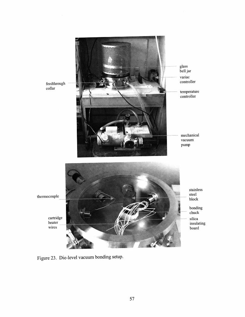
The die-level vacuum bonding apparatus is shown in Figure 21 and Figue 23. A
glass bell jar (Kurt J Lesker BJ1 2X18) sits on top of a stainless steel feedthrough collar
(Kurt J Lesker FTC 12-1-8-0) with a rubber gasket in between, which in turn sits on top
of a stainless steel base plate (Kurt J Lesker BASEPLATE12) with a rubber o-ring in
between. A mechanical roughing pump (Leybold Trivac B D25B) is connected to one
feedthrough to provide vacuum inside the bell jar. A pressure gauge (Kurt J Lesker 205
Thermocouple Controller + Kurt J Lesker 6000 Thermocouple Tube) is connected to
another feedthrough to monitor the pressure inside the bell jar.
A special stainless steel bonding chuck, shown in Figure 22, is made to align the
three-layer stack of the test structure. This two-piece chuck has pre-drilled holes for
cartridge heaters and thermocouple. The sample being bonded is placed inside the cavity
of the bottom piece and sandwiched by the top piece. Cartridge heaters (Omega
Engineering CSH-10 1100/120) are used to heat up the glass fit to its softening point of
550 C to initiate bonding. One or two stainless steel blocks (each 4.5 cm x 4 cm x 3 cm,
430 g) placed on top of the chuck are used to provide pressure (13.2 kPa with one, 26.4
kPa with two) to the bonding interface. A thermocouple (K type) is used to monitor the
temperature inside the chuck. The cartridge heaters and the thermocouple are connected
to the outside environment through feedthroughs.
Power to the cartridge heaters is provided by a variable-output transformer. This
power supply is controlled by a temperature controller (Omega Engineering CNi32)
through a solid state relay (Omega Engineering SSR240DC25). The controller regulates
55
8
the temperature by sending high (5 V) and low (0 V) signals to the relay to close and
open the circuit based on the thermocouple input.
glass bell jar
stainlesssteel block
bonding chuck
thermocouple
feedthrough
TCinput
controlwires
temperaturecontroller
Figure 21. Die-level vacuum bonding setup.
8.1 mm
10.1
1.2 mmdeep/
1/16" OD
25.2 mm
29.2mm
Figure 22. Top and cross sectional views of the bonding chuck.
56
silicainsulation
cartridgeheaters
uImvacuigauge
solidstaterelay
IIpowersupply
powersupply
Livanaccontroller
o o (
Fr-I
I I 1 1, 1 1 -, , I I - 7M7
feedthroughcollar
thermocouple_
cartridgeheaterwires
glassbell jar
variaccontroller
-- temperaturecontroller
mechanicalvacuum
pump
stainlesssteelblock
bondingchuck
silicainsulatingboard
Figure 23. Die-level vacuum bonding setup.
57

8.2 Bonding Procedure
First, the Vitta GPR-10 glass frit is taped onto the bonding surface of the top and
the bottom layers of the test structure. These two pieces are then heated up to 500 C for
15 minutes in air to burn off the organic binder (pre-sintering). After cooling down, the
glass frit covering the contact holes and the cavities are scraped off with a needle. A thin
channel in the glass frit can be created with a razor blade to provide an exit way for the
gases. The channel can be sealed once the glass frit flows at 550 C. However, this
channel is optional because air can exit through the gaps between two unbonded chips.
Next, all three layers of the test structure are placed into the cavity of the lower
half of the bonding chuck. The top half is then stacked on top, followed by one or two
stainless steel blocks. This whole assembly is placed onto an insulating silica board
inside the glass bell jar. Cartridge heaters and a thermocouple are inserted into the
appropriate holes on the bonding chuck.
The power output transformer and the temperature controller are then turned on.
Bonding follows the heating cycle shown in Figure 24. A 60 minute soak at 175-225 C is
intended to degas the silicon substrate, the glass frit, and the getter before bonding. Then,
the temperature is increased to 560-575 C to soften the glass frit for bonding.
560-575C
175-225
room temp-X room emp
20 mins 60 mins 40 mins 15 mins 60 mins
Figure 24. Heating cycle for the glass frit bonding.
58
8.3 Results
The resulting bond was very robust. The three-layer stack could not be separated
by a sharp razor blade. The alignment of the three layers was slightly off due to the
inexact fit of the dies in the cavity of the bonding chuck. Some glass fit over-flowed to
the sides of the stack and to cover some area under the contact holes, but electrical
conduction was not hindered.
In the first several bonding trials, the resistance of the metal line increased
dramatically (into the high kilo-ohm and low mega-ohm range) after the heating cycle.
The suspected causes were: (1) diffusion of silicon from the glass frit into the metal line
to form nonconductive silicide, (2) metal fracture induced by the thermal mismatch
between the metal and the glass frit. This problem was later solved with a ~300 nm thick
aluminum oxide (A120 3) diffusion barrier deposited on top of the metal. More details
about this problem and its solutions are presented in Section 9.
59
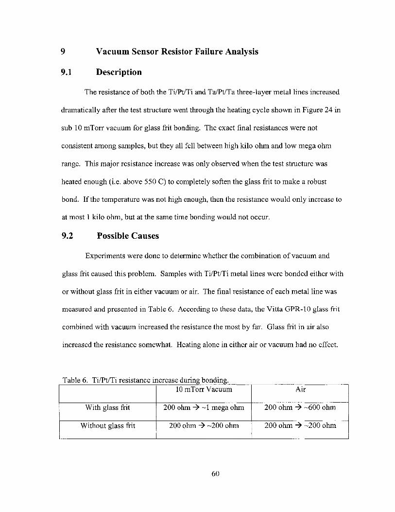
9 Vacuum Sensor Resistor Failure Analysis
9.1 Description
The resistance of both the Ti/Pt/Ti and Ta/Pt/Ta three-layer metal lines increased
dramatically after the test structure went through the heating cycle shown in Figure 24 in
sub 10 mTorr vacuum for glass frit bonding. The exact final resistances were not
consistent among samples, but they all fell between high kilo ohm and low mega ohm
range. This major resistance increase was only observed when the test structure was
heated enough (i.e. above 550 C) to completely soften the glass frit to make a robust
bond. If the temperature was not high enough, then the resistance would only increase to
at most 1 kilo ohm, but at the same time bonding would not occur.
9.2 Possible Causes
Experiments were done to determine whether the combination of vacuum and
glass frit caused this problem. Samples with Ti/Pt/Ti metal lines were bonded either with
or without glass frit in either vacuum or air. The final resistance of each metal line was
measured and presented in Table 6. According to these data, the Vitta GPR-10 glass frit
combined with vacuum increased the resistance the most by far. Glass frit in air also
increased the resistance somewhat. Heating alone in either air or vacuum had no effect.
Table 6. Ti/Pt/Ti resistance increase during bonding.10 mTorr Vacuum Air
With glass frit 200 ohm + -1 mega ohm 200 ohm 4 -600 ohm
Without glass frit 200 ohm -200 ohm 200 ohm 4 -200 ohm
60
The possible causes include: (1) silicon diffusion into the platinum metal line to
form nonconductive platinum silicide, and (2) physical fracturing of the metal line during
the heating cycle in vacuum.
The Vitta GPR-10 glass frit consists of zinc, lead, and borosilicate. Because the
glass frit was in direct contact with the metal during high-temperature bonding, silicon in
the glass frit could diffuse into the platinum layer through the grain boundaries of the
titanium layer to form nonconductive platinum silicide. This hypothesis was partially
confirmed by the Auger Electron Microscopy on some metal samples after the glass frit
was scraped off after bonding. The microscopy results did show some silicon signal in
the platinum layer, but due to the rough metal surface caused by scraping, these results
were not very reliable.
Thermal mismatch between the glass frit (thermal expansion coefficient = 6.5 x
10-6) and the three-layer metal line (thermal expansion coefficients of Ti = 9.2 x 10⁻⁶ and
of Pt = 8.9 x 10⁻⁶) could fracture the metal during temperature ramp down because the
glass frit was already tightly bonded to the metal at the time of temperature ramp down.
The stainless steel weight used to facilitate bonding also added an extra strain on the
metal.
Silicon diffusion is believed to be the major cause of the resistance increase based
on the following observations:
1. Thermal mismatch alone can not explain why the resistance did not increase as much
when the sample was bonded in air as in vacuum. If the thermal mismatch alone was
the problem, then the resistances should have increased to the same level both in
vacuum and in air.
61

2. Masahiro has shown that the diffusion of titanium in gold films increased with
lowering vacuum.1 7 This finding can explain the observation that the resistance
increased much more in vacuum than in air.
9.3 Solutions
9.3.1 Tantalum Nitride (TaN) Diffusion Barrier
One possible solution to deter diffusion is to deposit a layer of TaN diffusion
barrier on top of the middle (vacuum sensor) dies by reactive sputtering. The
composition of TaN can be controlled by adjusting the supply of nitrogen gas during
sputtering. The resulting TaN will become less conductive and a better diffusion barrier
with more nitrogen gas present. It is important to have a nonconductive diffusion barrier
in this case in order to prevent short circuiting the various metal lines on the vacuum
sensor die.
10 sccm nitrogen and 40 sccm argon were supplied into the sputterer to make a
~300 nm thick TaN layer. However, the resistance of the resulting TaN turned out to be
comparable to that of the metal line, which was not acceptable. In addition, several
bonding trials with the TaN-coated sensor dies produced resistance values from 20K to
30K ohm, which was still too high for the sensor to function. This indicated the poor
performance of this specific TaN composition as a diffusion barrier.
9.3.2 Aluminum Oxide (A120 3) Diffusion Barrier
~300 nm thick A120 3 was deposited onto the vacuum sensor dies with a shadow
mask by electron beam evaporation, shown in Figure 25. The positive results of the six
bonding trials shown in Table 7 indicated the ability of A12 0 3 to stop diffusion.
62
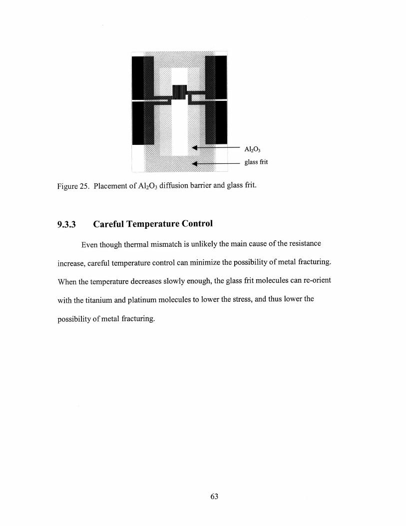
* ~ A120 3
glass frit
Figure 25. Placement of A120 3 diffusion barrier and glass frit.
9.3.3 Careful Temperature Control
Even though thermal mismatch is unlikely the main cause of the resistance
increase, careful temperature control can minimize the possibility of metal fracturing.
When the temperature decreases slowly enough, the glass frit molecules can re-orient
with the titanium and platinum molecules to lower the stress, and thus lower the
possibility of metal fracturing.
63
10
10.1
Evaluation of Vacuum Package
Summary
Six samples of the second generation test structure (i.e. 10 nm thick Ta/400 nm
thick Pt/20 nm thick Ta metal structure with 300 nm thick A120 3 diffusion barrier on top)
were bonded in 10 mTorr vacuum. No gas exit channel was created in the glass frit.
Based on the vacuum sensor measurements and the leak tests, no vacuum was retained in
any of the samples after leaving the vacuum environment.
The SAES St122 NEG had no effect on the vacuum level due to the premature
saturation caused by a high base pressure inside the test structure (i.e. 1 ATM). Getters
typically need to operate at a base pressure of 10-2 Torr or lower to prevent premature
saturation.
10.2 Vacuum Sensor Measurements
The vacuum sensor measurements of the six samples within one hour after
leaving the vacuum environment are summarized in Table 7, where V and I, are used to
calculate the base resistance R, = V,/10 initially, Target is the target temperature, Rtarget is
the target resistance calculated with Equation 12, V and I are measurements taken to
calculate R = V/I (to match Rtarget), and Q is the required power input to maintain Ttarget.
These measurements can not pinpoint the exact pressures inside the samples
because the sensor has zero resolution above roughly 50 Torr, which is a characteristic of
all thermal conductivity based vacuum sensors. In addition, because the calibration
curves of different sensor samples exhibit discrepancies of up to 18% in the high pressure
range, it is difficult to correlate these high sensor readings to the actual pressures.
64

Table 7. Bonding parameters and vacuum sensor measurement for each sample.Measurement taken within one hour after each sample left vacuum environment.
Sample #1 #2 #3 #4 #5 #6
Prebake Time 60 60 0 0 0 0[min]
Prebake 150-190 150-185 n/a n/a n/a n/aTemp[C]
Bonding 15 15 15 15 15 15Time[min]
Bonding 550-560 550-562 560-565 555-560 553-562 550-570Temp[C]
# Weight 1 1 1 1 1 2BlocksGetter? No Yes No Yes No No
Rbeore 116 116 113 110 112 115[ohm]Rafer 322 146 192 165 190 187[ohm]
VO 20.2 18.6 25.2 54.6 34.0 13.2[mV_]
10 0.067 0.144 0.142 0.379 0.196 0.080[mA]
R) 301.5 129.0 177.3 144.2 173.4 165.0[ohm]Ttarget 87 87 87 87 87 87
[C]TCR 0.26 0.26 0.26 0.26 0.26 0.26[%/C]Rtarget 349.7 149.7 205.7 167.3 201.3 191.4[ohm]
V 6.94 3.67 4.43 4.15 4.41 4.11
[V]1 19.86 24.56 21.76 24.78 21.9 21.5
IPA]R 349.6 149.6 203.5 167.3 201.3 191.6
[ohm}_]Q '137.8 90.2 96.3 102.7 96.0 88.3
[niW]P ~50-760 -50-760 -50-760 ~50-760 -50-760 ~50-760
[Torr]
65

10.3 Leak Tests
This leak test involves placing the bonded sample into a vacuum chamber,
pumping down the chamber, and then taking a measurement with the vacuum sensor. If
the sensor reading indicates a lower pressure than before, then that means some gases
have exited the structure through the leaks in the glass frit. If the pressure stays the same
as before, than that means the seal is hermetic and the high pressure inside the structure is
probably caused by the outgassing from the internal surfaces and the glass frit itself.
As shown in Table 8, the leak tests confirmed that none of the six samples
achieved a hermetic seal. However, the rate of gas movement across the seal was
significantly slowed down. For example, when the leak test was conducted on Sample #5
within 1 hour after pump down, the pressure inside the structure remained at 3.5 Torr
while the pressure in the chamber was only 50 mTorr. Roughly one day after pump
down, the internal pressure reached 94 mTorr while the external pressure was 10 mTorr.
Table 8a. Leak test results (Measured within 1 hour after pump down).Sample #1 #2 #3 #4 #5 #6
Chamber 25 25 20 50 50 30Pressure mTorr mTorr mTorr mTorr mTorr mTorr
Sensor 3.09 1.82 1.97 3.38 22.45 2.35Reading mW mW mW mW mW mW
Pressure 118 ±2.4 52 ±1.0 60 ±1.2 135 ±2.7 3.5 ±1 82 ±1.6Inside mTorr mTorr mTorr mTorr Torr mTorr
Structure
66
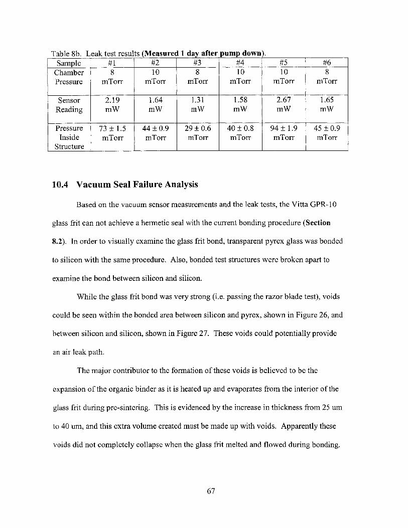
Table 8b. Leak test results (Measured 1 day after pump down).Sample #1 #2 #3 #4 #5 #6
Chamber 8 10 8 10 10 8Pressure mTorr mTorr mTorr mTorr mTorr mTorr
Sensor 2.19 1.64 1.31 1.58 2.67 1.65Reading mW mW mW mW mW mW
Pressure 73 ± 1.5 44 ±0.9 29 ±0.6 40 ±0.8 94 ±1.9 45 ±0.9Inside mTorr mTorr mTorr mTorr mTorr mTorr
Structure
10.4 Vacuum Seal Failure Analysis
Based on the vacuum sensor measurements and the leak tests, the Vitta GPR-10
glass frit can not achieve a hermetic seal with the current bonding procedure (Section
8.2). In order to visually examine the glass frit bond, transparent pyrex glass was bonded
to silicon with the same procedure. Also, bonded test structures were broken apart to
examine the bond between silicon and silicon.
While the glass frit bond was very strong (i.e. passing the razor blade test), voids
could be seen within the bonded area between silicon and pyrex, shown in Figure 26, and
between silicon and silicon, shown in Figure 27. These voids could potentially provide
an air leak path.
The major contributor to the formation of these voids is believed to be the
expansion of the organic binder as it is heated up and evaporates from the interior of the
glass frit during pre-sintering. This is evidenced by the increase in thickness from 25 um
to 40 um, and this extra volume created must be made up with voids. Apparently these
voids did not completely collapse when the glass frit melted and flowed during bonding.
67
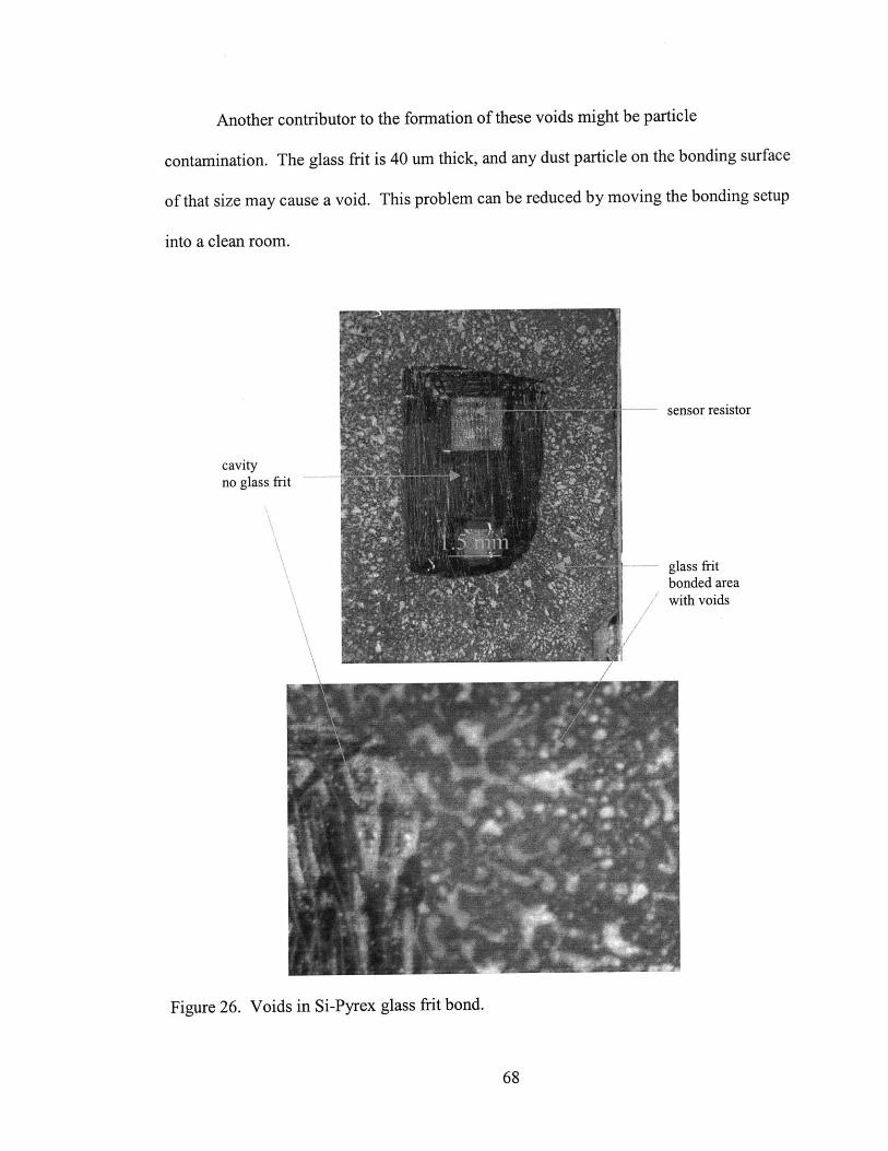
Another contributor to the formation of these voids might be particle
contamination. The glass flit is 40 um thick, and any dust particle on the bonding surface
of that size may cause a void. This problem can be reduced by moving the bonding setup
into a clean room.
sensor resistor
cavityno glass frit
glass fritbonded areawith voids
Figure 26. Voids in Si-Pyrex glass frit bond.
68
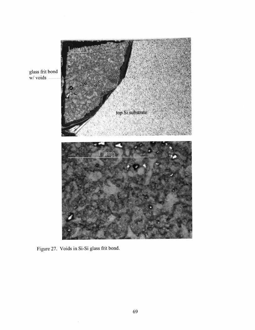
glass frit bondw/ voids
Figure 27. Voids in Si-Si glass frit bond.
69

11 Future Work
The Vitta GPR- 10 glass frit can not achieve a hermetic seal with the current
bonding procedure. The suspected cause is the voids formed in the glass frit by the
organic binder. Some bonding parameters can be changed to try to reduce the voids.
First, the glass frit can be pre-sintered at a higher temperature for a longer time to
completely burn off the binder before bonding. Second, the bonding temperature and
time can be increased to make sure that the glass frit is completely melted during
bonding, which can help compress the voids. Third, contact pressure onto the bonding
surface can be increased (by adding more weight on top) to help compress the voids and
form a tighter bond.
Even if the Vitta GPR-10 can not achieve a hermetic seal after adjusting the
bonding parameters, other glass frit materials are still available for future studies. An
attractive alternative would be a continuous glass preform without any binder. This way
the void problem may be completely avoided.
A different bonding method worth an investigation is the solder bonding. Solder
(e.g. tin, lead, indium, gold) has the same flow characteristics as the glass frit, making it
ideal for bonding over rough surfaces, and the resulting metallic bond is known to
provide a strong seal. H. Tilmans, M. Van de Peer, and E. Beyne have successfully
created a vacuum package with solder bonding.5 However, for the current test structure
and the actual suspended tube reactor, an insulating layer (e.g. silicon dioxide, silicon
nitride, tantalum nitride, etc.) must be deposited on top of the resistor line, as shown in
Figure 28, to prevent short circuit by the electrically conductive solder. Also, the
70

- urn
relatively low melting point of a solder would limit the operating temperature of the
reactor.
insulating layer (e.g. SiO 2)
solder ring (e.g. Sn/Pb) on top ofwettable metal (e.g. Au)
Figure 28. Possible implementation of solder bonding on test structure.
In solder bonding, wettable metal pads need to be first deposited over the non-
wettable silicon surface. This wettable metal usually comprises three layers: an adhesion
metal (e.g. chromium or titanium), a barrier metal (e.g. copper or platinum), and a
sacrificial metal (e.g. gold). The barrier metal is required to prevent the solder from
dissolving the adhesion metal. Then, solder (e.g. tin/lead, indium, gold) is deposited over
the wettable metal. After contacting the two surfaces and heating to the melting point of
the solder (i.e. 250-350 C), the solder begins to flow and bonds the two surfaces.5
After working out a robust bonding method on the test structure, it will be
important to apply the same technique to packaging the actual suspended tube reactor.
The amount of getter required may be different since they may have different surface
area-to-volume ratios. Also, if another material is found to have a longer life time than
71

platinum under high temperatures, then the replacement will potentially alter the resistor
thickness, and whether the glass frit or the solder can still form a hermetic seal will need
to be investigated once again.
72
12 Conclusion
The purpose of this thesis project is to study the feasibility of selected vacuum
packaging methods, including a wafer bonding method that can provide a hermetic seal
over a rough surface in vacuum (i.e. -400 nm thick roughness), a gettering method that
can best absorb residual gases inside the package after bonding, and a vacuum sensing
method that can provide adequate sensitivity in the range of interest in order to confirm
the final pressure inside the package. Based on the results of literature search, a three-
layer test structure is built to experiment with glass frit bonding (Vitta GPR- 10 glass frit),
non-evaporable getter (SAES St122 NEG, mixture of Ti and Zr-V-Fe), and thermal
conductivity vacuum sensor. The main conclusion from this study is that the Vitta GPR-
10 glass frit can not achieve a hermetic seal with the current bonding procedure. The
vacuum sensor measurements, along with the leak tests, indicated atmospheric pressure
inside the test structure. And because the pressure inside the structure was too high, the
SAES St122 NEG quickly saturated and failed. Getters typically need to operate at a
base pressure of 102 Torr or lower, and any pressure higher than that would result in
premature saturation. For future work, various bonding parameters for the GPR- 10 can
be adjusted to try to make a better seal, and other bonding methods, such as solder
bonding, can be examined. The effectiveness of the SAES St122 NEG can only be
known when a robust hermetic seal is achieved to maintain a reasonable base pressure
inside the test structure.
73

13 References
1 K. Jensen, "Integrated Chemical Fuel Microprocessor for Power Generation inMEMS Applications," Quarterly Report for 2/1/2000-4/31/2001, MIT, 2001.
2 N. Maluf, An Introduction to Microelectromechanical Systems Engineering, Boston,MA: Artec House, 2000.
3 M. Schmidt, "Wafer-to-Wafer Bonding for Microstructure Formation," Proceedingsof the IEEE, Volume 86, Number 8, 1998.
4 W. Ko, J. Suminto, and G. Yeh, "Bonding Techniques for Microsensors," inMicromachining and Micropackaging of Transducers, C. Fung, P. Cheung, W. Ko,and D. Fleming, Amsterdam, The Netherlands: Elsevier, 1985.
5 H. Tilmans, M. Van de Peer, and E. Beyne, "The Indent Refloww Sealing Technique-A Method for the Fabrication of Sealed Cavities for MEMS Devices," Journal ofMicroelectromechanical Systems, Volume 9, Issue 2, 2000.
6 D. Hoffman, B. Singh, and J. Thomas, Handbook of Vacuum Science andTechnology, San Diego, CA: Academic Press, 1998.
7 T. Giorgi, B. Ferrario, and B. Storey, "An Updated Review of Getters and Gettering,"Journal of Vacuum Science and Technology A, Volume 3, Issue 2, 1985.
8 L. Parameswaran, "Silicon Pressure Sensor Using Wafer Bonding Technology," MSThesis, MIT, 1993.
9 M. Esashi, S. Sugiyama, K. Ikeda, Y. Wang, and H. Miyashita, "Vacuum-SealedSilicon Micromachined Pressure Sensors," Proceedings of the IEEE, Volume 86,Number 8, 1998.
10 A. Robinson, P. Haswell, and R. Lawson, "A Thermal Conductivity MicrostructuralPressure Sensor Fabricated in Standard Complementary Metal OxideSemiconductor," Review of Scientific Instruments, Volume 63, Issue 3, 1992.
11 R. Gooch, T. Schimert, W. McCardel, and B. Ritchey, "Wafer-Level VacuumPackaging for MEMS," Journal of Vacuum Science and Technology A, Volume 17,Issue 4, 1999.
12 H. Henmi, S. Shoji, Y. Shoji, K. Yoshimi, and M. Esashi, "Vacuum Packaging forMicrosensors by Glass-Silicon Anodic Bonding," Sensors and Actuators A, Volume43, 1994.
13 P. Atkins, Physical Chemistry, New York, NY: Freeman, 1991.
74
14 0. Paul, 0. Brand, R. Lenggenhager, and H. Baltes, "Vacuum Gauging withComplementary Metal-Oxide-Semiconductor Microsensors," Journal of VacuumScience and Technology A, Volume 13, Issue 3, 1995.
15 S. Firebaugh, "Investimation of Materials for Use in High-Temperature, Thin-FilmHeaters and Temperature Sensors," MS Thesis, MIT, 1997.
16 F. Incropera and D. DeWitt, Fundamentals ofHeat and Mass Transfer, New York,NY: Wiley, 1996.
17 K. Masahiro and S. Noboru, "Effects of Temperature, Thickness and Atmosphere onMixing in Au-Ti Bilayer Thin Films," 1993.
18 Nanonics Imaging Ltd (http://www.nanonics.co.il/cont/probes/wired.html).
75
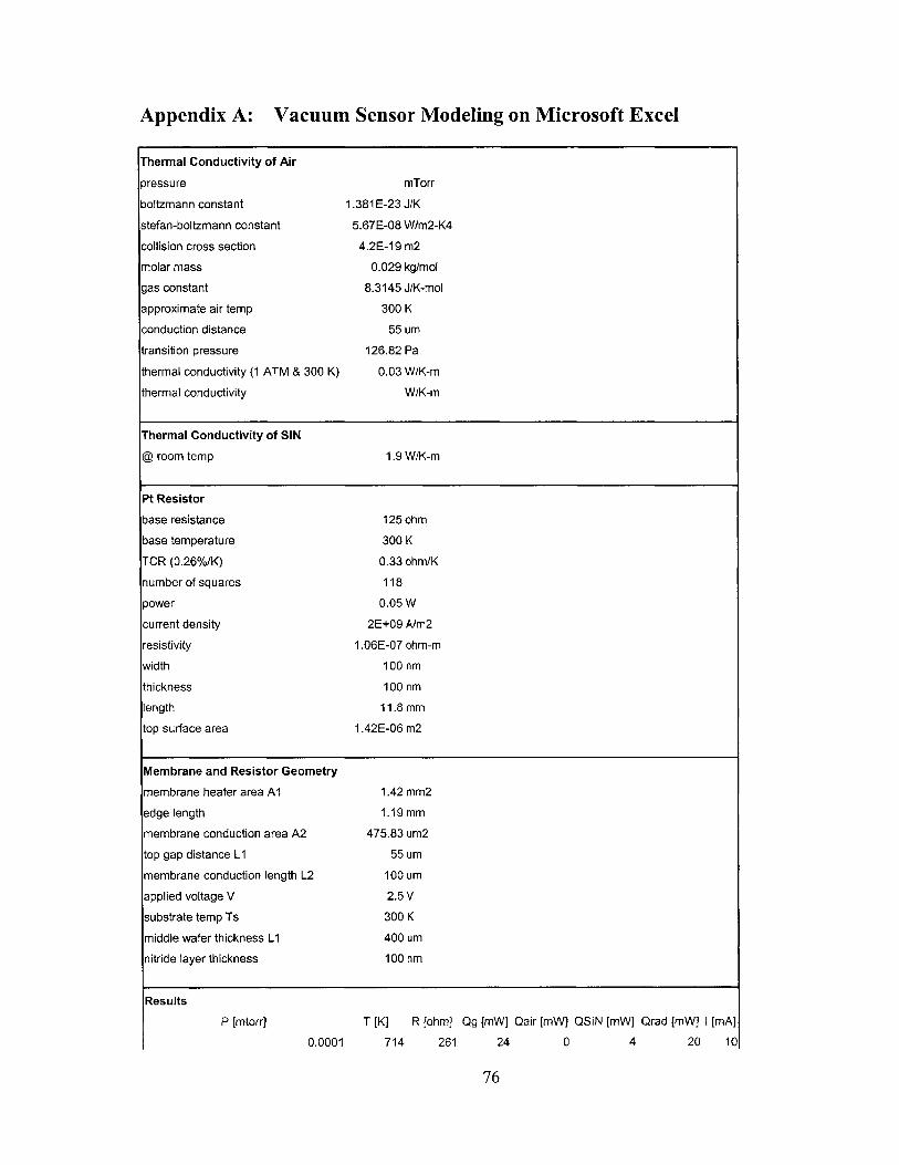
Appendix A: Vacuum Sensor Modeling on Microsoft Excel
Thermal Conductivity of Air
pressure
boltzmann constant
stefan-boltzmann constant
collision cross section
molar mass
gas constant
approximate air temp
conduction distance
transition pressure
thermal conductivity (1 ATM & 300 K)
thermal conductivity
Thermal Conductivity of SiN
@ room temp
Pt Resistor
base resistance
base temperature
TCR (0.26%/K)
number of squares
power
current density
resistivity
width
thickness
length
top surface area
mTorr
1.381 E-23 J/K
5.67E-08 W/m2-K4
4.2E-1 9 m2
0.029 kg/mol
8.3145 J/K-mol
300 K
55 um
126.82 Pa
0.03 W/K-m
W/K-m
1.9 W/K-m
125 ohm
300 K
0.33 ohm/K
118
0.05 W
2E+09 A/m2
1.06E-07 ohm-m
100 nm
100 nm
11.8 mrn
1.42E-06 m2
Membrane and Resistor Geometry
membrane heater area Al
edge length
membrane conduction area A2
top gap distance LI
membrane conduction length L2
applied voltage V
substrate temp Ts
middle wafer thickness Li
nitride layer thickness
P [mtorr]
0.0001
1.42 mm2
1.19 mm
475.83 um2
55 um
100 urn
2.5 V
300 K
400 um
100 nm
T [K] R [ohm] Qg [mW] Qair [mW] QSiN [mW] Qrad [mW] I [mA]
714 261 24 0 4 20 10
76
Results
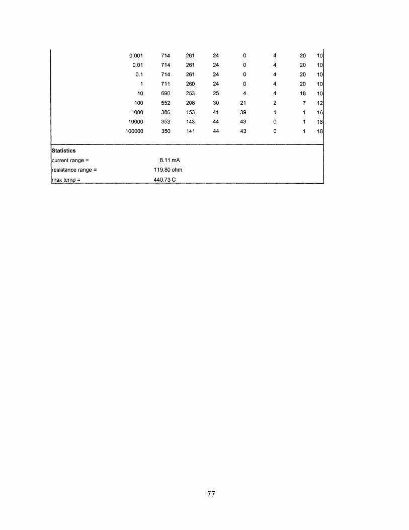
0.001
0.010.1
1
10
100
1000
10000100000
714
714
714
711
690
552
386
353
350
261
261
261
260
253
208
153
143
141
24
24
24
24
25 4
30
41
44
44
4 18 10
Statistics
current range = 8.11 mA
resistance range = 119.80 ohm
max temp = 440.73 C
77
0
0
0
0
4
4
4
4
20 10
20 Ic
20 1C
20 1C
21
39
43
43
2
1
0
0
7 12
1 16
I 18
I 18

Appendix B: Test Structure Mask Drawings on AutoCAD
Mask 1: Top Layer, Front Side - Sensor CavityBottom Layer, Front Side - Getter Room
78
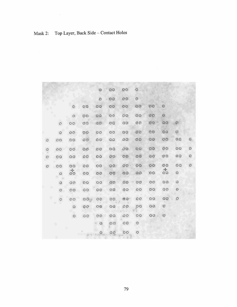
Mask 2: Top Layer, Back Side - Contact Holes
O 00 o00 0 0
00, 0 0
0 01 -00 '00 010 -0.via
o 00 00 00' 00o 00 00 o " Orp
o 0 0 00(- 010 4 0 9
0 C 00 0 0 00 00 0
0 00 0 0 00 06 I 00 0
0 00 .0 o 00 0 - 00 0, 0 00 0
0 0:0 00
0 00
00 0 c 0O 10 o0 0 0
00 0 @ 00, 0 0 00, 00 0
0 00 00 00 00 00
0 00 00 00 00 00 00
o oo o6-t 00
0 Q0 0@
00. 001 00
o00 pGQO
00 00 0.
00 00 0,
00, 0 0
0I 0
0 00 00 '00. 00 00
c& 9 00 0
0.0,d
79
00 , 0
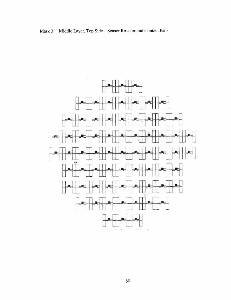
Mask 3: Middle Layer, Top Side - Sensor Resistor and Contact Pads
I-' ~L ww:[LWL
Li iif L IW
HHI+HH77 F'UHU U H LFHI
HH7
80

Mask 4: Middle Layer, Back Side - KOH Etch and Pressure Equalization Holes
I..
LiLi
...
El
E
DLi
Li
EEIi]0.Li
Li
Li
LiLI
L
Li
Li
El
l
ID
IIILi
LI
Li
LiLi
E
L]
EL
DLEL
EL
Li
LiLi
0ILi
LiL]
LiLi
L
[11
l
E]
E]
l
Li
LiLi
l
L-I
E
LiLi
LiLi
LiLi
LiLi
LiLi
K]F.
LiLi
Li
Li
E]Li
LiLi
LiLi
LI]Li
LiLi
LiLI
Li
Li
Li
Li
Li
LI]
Li
Li
Liii
L]Li
LiLi
LiLi
LILi
L..i
E
Li
81
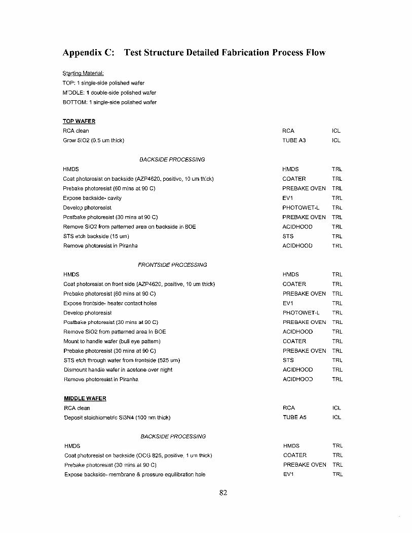
Appendix C: Test Structure Detailed Fabrication Process Flow
Starting Material:
TOP: 1 single-side polished wafer
MIDDLE: 1 double-side polished wafer
BOTTOM: 1 single-side polished wafer
TOP WAFER
RCA clean
Grow SiO2 (0.5 urn thick)
BACKSIDE PROCESSING
HMDS
Coat photoresist on backside (AZP4620, positive, 10 um thick)
Prebake photoresist (60 mins at 90 C)
Expose backside- cavity
Develop photoresist
Postbake photoresist (30 mins at 90 C)
Remove SiO2 from patterned area on backside in BOE
STS etch backside (15 um)
Remove photoresist in Piranha
FRONTSIDE PROCESSING
HMDS
Coat photoresist on front side (AZP4620, positive, 10 um thick)
Prebake photoresist (60 mins at 90 C)
Expose frontside- heater contact holes
Develop photoresist
Postbake photoresist (30 mins at 90 C)
Remove SiO2 from patterned area in BOE
Mount to handle wafer (bull eye pattern)
Prebake photoresist (30 mins at 90 C)
STS etch through wafer from frontside (525 um)
Dismount handle wafer in acetone over night
Remove photoresist in Piranha
MIDDLE WAFER
RCA clean
Deposit stoichiometric Si3N4 (100 nm thick)
BACKSIDE PROCESSING
HMDS
Coat photoresist on backside (OCG 825, positive, 1 um thick)
Prebake photoresist (30 mins at 90 C)
Expose backside- membrane & pressure equilibration hole
HMDS
COATER
PREBAKE OVEN
EV1
PHOTOWET-L
PREBAKE OVEN
ACIDHOOD
STS
ACIDHOOD
HMDS
COATER
PREBAKE OVEN
EV1
PHOTOWET-L
PREBAKE OVEN
ACIDHOOD
COATER
PREBAKE OVEN
STS
ACIDHOOD
ACIDHOOD
RCA
TUBE A5
HMDS
COATER
PREBAKE OVEN
EV1
82
RCA
TUBE A3
ICLICL
TRL
TRL
TRL
TRL
TRL
TRL
TRL
TRL
TRL
TRL
TRL
TRL
TRL
TRL
TRL
TRL
TRL
TRL
TRL
TRL
TRL
ICLICL
TRL
TRL
TRL
TRL
Develop photoresist
Postbake photoresist (30 mins at 120 C)
Pattern Si3N4
Remove photoresist in Piranha
PHOTOWET-L
POSTBAKE OVEN
AME5000
ACIDHOOD
FRONTSIDE PROCESSING
HMDS
Coat photoresist on frontside (image reversal, negative, 1.5 um thick-2200 rpm spin)
Prebake photoresist (30 mins at 90 C)
Expose frontside- metal heater (1.5 sec)
Place wafers on hotplate (90 sec)
Flood Expose (1 min)
Develop photoresist
UVOzone cleanAsh
Deposit 10 nm Ta/400 nm Pt/20 nm Ta
Lift-off
Nanostrip
HMDS
COATER
PREBAKE OVEN
EV1
POSTBAKE OVEN
EV1
PHOTOWET-L
UVOZONEASHER
E-BEAM
PHOTOWET-R
ACIDHOOD
KOH etch through wafer from backside in sealed holder, stopping on frontside Si3N4 layer KOH
Post KOH clean in Nanostrip & first half of RCA ACIDHOOD
Anneal metal (60 mins at 650 C) TUBE B1
BOTTOM WAFER
No processing needed
BACKSIDE PROCESSING
FRONTSIDE PROCESSING
HMDS
Coat photoresist on frontside (AZP4620, positive, 10 um thick)
Prebake photoresist (60 mins at 90C)
Expose backside- cavity
Develop photoresist
Postbake photoresist (30 mins at 90C)
Remove SiO2 from patterned area on frontside in BOE
STS etch backside (225 um)
Remove photoresist in Piranha
HMDS
COATER
PREBAKE OVEN
EV1
PHOTOWET-L
PREBAKE OVEN
ACIDHOOD
STS
ACIDHOOD
83
TRL
TRL
ICLTRL
TRL
TRL
TRL
TRL
TRL
TRL
TRL
TRL
TRL
TRL
TRL
SGL
TRL
TRL
TRL
TRL
TRL
TRL
TRL
TRL
TRL
TRL
TRL
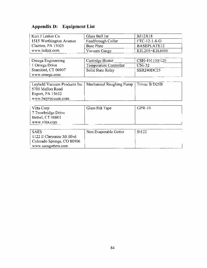
Appendix D: Equipment List
Kurt J Lesker Co Glass Bell Jar BJ12X181515 Worthington Avenue Feedthrough Collar FTC-12-1-8-0Clairton, PA 15025 Base Plate BASEPLATE12www.lesker.com Vacuum Gauge KJL205+KJL6000
Omega Engineering Cartridge Heater CSH-101100/1201 Omega Drive Temperature Controller CNi-32Stamford, CT 06907 Solid State Relay SSR240DC25www.omega.com
Leybold Vacuum Products Inc Mechanical Roughing Pump Trivac B D25B5700 Mellon RoadExport, PA 15632www.buyvacuum.com
Vitta Corp Glass Frit Tape GPR-107 Trowbridge DriveBethel, CT 06801www.vitta.com
SAES Non Evaporable Getter St1221122 E Cheyenne Mt BlvdColorado Springs, CO 80906www.saesgetters.com
84
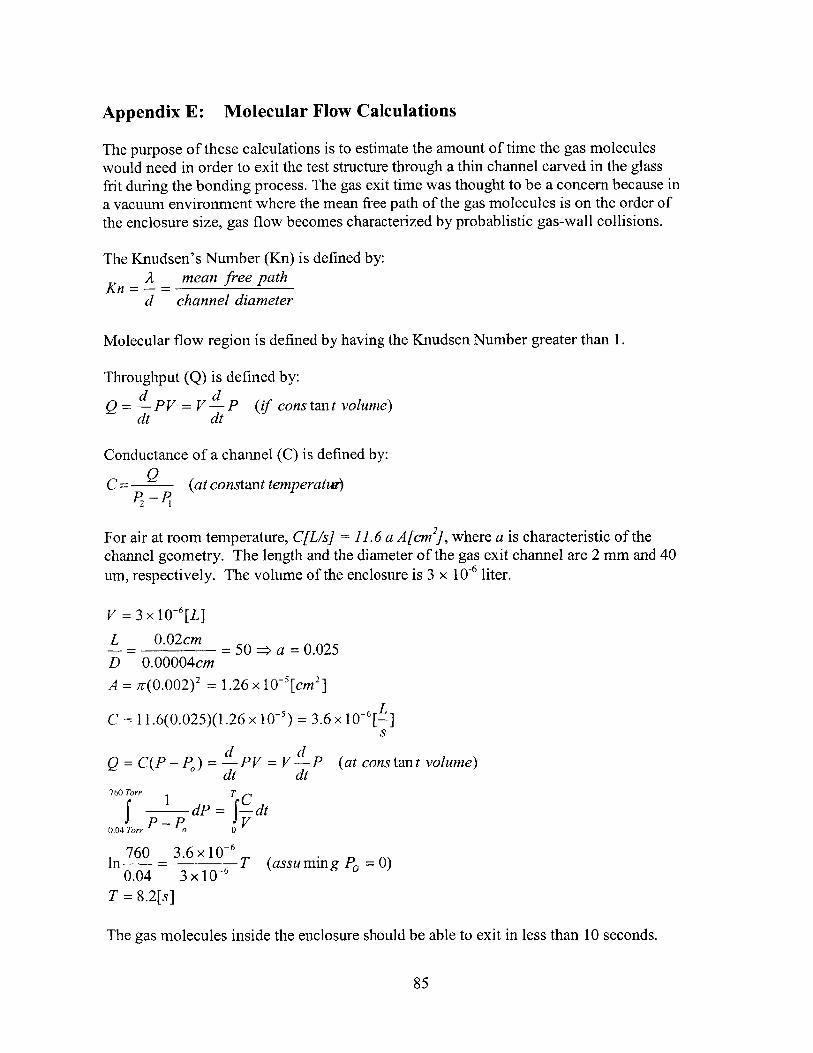
Appendix E: Molecular Flow Calculations
The purpose of these calculations is to estimate the amount of time the gas moleculeswould need in order to exit the test structure through a thin channel carved in the glassfrit during the bonding process. The gas exit time was thought to be a concern because ina vacuum environment where the mean free path of the gas molecules is on the order ofthe enclosure size, gas flow becomes characterized by probablistic gas-wall collisions.
The Knudsen's Number (Kn) is defined by:
Kn = A = mean free pathd channel diameter
Molecular flow region is defined by having the Knudsen Number greater than 1.
Throughput (Q) is defined by:d dQ -PV = V -P (if cons tant volume)dt dt
Conductance of a channel (C) is defined by:
C= Q (at constant temperatur)
For air at room temperature, C[L/s] = 11.6 a A[cm2], where a is characteristic of thechannel geometry. The length and the diameter of the gas exit channel are 2 mm and 40um, respectively. The volume of the enclosure is 3 x 10⁻⁶ liter.
V = 3x10⁻⁶L]
L 0.02cm-- = =50 --> a = 0.025
D 0.00004cm
A = r(0.002) 2 = 1.26 x 10~5[cm 2]
C = 11.6(0.025)(1.26 x 10 5 ) = 3.6 x 10⁻⁶[]
d dQ =C(P - P) = -PV= V P (at cons tan t volume)
dt dt760 Torr TJ dP =J-dt0.04 Torr O 0
760 _3.6 x10-6in = T (assu ming PO = 0)
0.04 3 x 10- 6
T = 8.2[s]
The gas molecules inside the enclosure should be able to exit in less than 10 seconds.
85

Experimental Data on the Target Pressure
2.8
15 V2.6 -
E. 1*- 40 mTorr05 2.4 -
CO)-j 2.2-
2.0 -CUa)
1.8-
1.6 -
1.E-06 1.E-05 1.E-04 1.E-03 1.E-02 1.E-01 1.E+00 1.E+01
Ambient Pressure (Torr)
The above graph shows that a vacuum of 40 mTorr or less is desirable in order tominimize heat loss. At 40 mTorr or less, heat loss becomes independent of pressure for
the geometry of the suspended tube reactor, and achieving a pressure lower than that will
not further decrease heat loss.
86
Appendix F: