A Smart IoT Node using a Hybrid Edge-Computing Strategy ...
129
André Mendes Antunes Licenciado em Ciências de Engenharia Eletrotécnica e de Computadores A Smart IoT Node using a Hybrid Edge-Computing Strategy for Environmental Multiparameter Sensing Dissertação para obtenção do Grau de Mestre em Engenharia Eletrotécnica e de Computadores Orientador: João Pedro Abreu de Oliveira, Prof. Doutor, Universidade Nova de Lisboa - Faculdade de Ciências e Tecnologia Júri Presidente: Doutor João Almeida das Rosas - FCT/UNL Arguentes: Doutor Nuno Filipe Silva Veríssimo Paulino - FCT/UNL Doutor João Pedro Abreu de Oliveira - FCT/UNL Março, 2021
Transcript of A Smart IoT Node using a Hybrid Edge-Computing Strategy ...

André Mendes Antunes
Licenciado em Ciências deEngenharia Eletrotécnica e de Computadores
A Smart IoT Node using a HybridEdge-Computing Strategy for Environmental
Multiparameter Sensing
Dissertação para obtenção do Grau de Mestre em
Engenharia Eletrotécnica e de Computadores
Orientador: João Pedro Abreu de Oliveira, Prof. Doutor, UniversidadeNova de Lisboa - Faculdade de Ciências e Tecnologia
Júri
Presidente: Doutor João Almeida das Rosas - FCT/UNLArguentes: Doutor Nuno Filipe Silva Veríssimo Paulino - FCT/UNL
Doutor João Pedro Abreu de Oliveira - FCT/UNL
Março, 2021

A Smart IoT Node using a Hybrid Edge-Computing Strategy for Environmen-tal Multiparameter Sensing
Copyright © André Mendes Antunes, Faculty of Sciences and Technology, NOVA Univer-
sity Lisbon.
The Faculty of Sciences and Technology and the NOVA University Lisbon have the right,
perpetual and without geographical boundaries, to file and publish this dissertation
through printed copies reproduced on paper or on digital form, or by any other means
known or that may be invented, and to disseminate through scientific repositories and
admit its copying and distribution for non-commercial, educational or research purposes,
as long as credit is given to the author and editor.
Este documento foi gerado utilizando o processador (pdf)LATEX, com base no template “novathesis” [1] desenvolvido no Dep. Informática da FCT-NOVA [2].[1] https://github.com/joaomlourenco/novathesis [2] http://www.di.fct.unl.pt


"I’ve actually not read any books on time management."- Elon Musk


Acknowledgements
First of all i would like to express my gratitude to my supervisor Professor João Pedro
Oliveira for his hard work, support and advice throughout this dissertation. In spite of
the ongoing pandemic and the difficult situation we faced, he always managed to provide
prompt help and guidance, which lead to the results that were achieved.
I would also like to thank my parents, mostly for creating me, but also for their
patience, support and prompt reminders to keep myself fed throughout these five years.
Thanks to my cousin, as well, for his patience and ready availability to read and
spellcheck this dissertation about a subject completely foreign to him.
And lastly, thank you to all my friends who provided fun, entertaining, memorable,
but also sometimes weird moments which helped me keep some glimmer of mental sanity
throughout the whole college experience.
vii

Abstract
The Internet of Things (IoT) has been growing at an immense pace over the last few
years and there are no predictions of slowing down anytime soon, but most importantly,
not only has it been growing in size but it has also been growing in capabilities, per-
formance and diversity. Diversity is incredibly important but also fracturing, in this
context. As IoT sensor nodes get more performant and diverse, their adaptability and
reconfigurability ends up being lost in the search for ultimate performance.
As a way to unify these individual single purpose sensor nodes, a need and an oppor-
tunity present themselves to develop a singular multi-parameter, multi-sensor IoT node,
that can make use of the latest reconfigurable technology to adapt itself to the require-
ments of each type of sensor, while maintaining the very high performance and precision
of dedicated sensor nodes.
This dissertation work will thus focus on developing an architecture and building a
prototype circuit board for a multi-sensor, reconfigurable IoT node based on a state-of-
the-art System-on-Chip (SoC) with extremely high resolution measurement capabilities,
which can interface with virtually any type of existing sensor. This architecture and
prototype are intended to serve as a stepping stone in the path to develop a capable IoT
node which can interface with a wider range of sensor and have a higher precision than
what is currently available.
Keywords: IoT, Sensor Node, Flexible, Reconfigurable, High-Precision, SoC
ix

Resumo
A Internet of Things (IoT) tem vindo a crescer a passos largos ao longo dos últimos
anos, e não apresenta quaisquer sinais de abrandar o seu crescimento num futuro próximo.
No entanto, não só tem vindo a crescer em tamanho, mas também nas suas capacidades,
performance e diversidade. Enquanto que a diversidade é extremamente importante,
neste contexto, é também fraturante. À medida que os nós IoT melhoram em performance
e diversidade, a sua adaptabilidade e reconfigurabiliade acaba por ficar em segundo plano
na procura do pico de performance.
Com o objetivo de unificar estes nós de sensores com propósitos singulares, apresenta-
se uma oportunidade e uma necessidade de desenvolver um único nó IoT capaz de fazer
interface com uma multiplicidade de sensores distintos, usando tecnologia de ponta re-
configurável para se adaptar às necessidades de cada tipo de sensor, mantendo ainda
assim a alta performance e precisão de nós de sensor dedicados.
A presente dissertação irá então focar-se no desenvolvimento de uma arquitetura
de sistema e criação de um protótipo em placa de circuito impresso referente a um nó
IoT multisensor reconfigurável, baseado num SoC de última geração com capacidades de
medição extremamente elevadas, que consiga fazer interface com qualquer tipo de sensor
existente. Esta arquitetura de sistema e protótipo são desenvolvidos com a intenção de
servirem como ponto de partida para o desenvolvimento de um nó IoT de interface com
sensores, que tenha a capacidade de medir qualquer tipo de sensor com uma precisão
superior àquilo que está atualmente disponível.
Palavras-chave: IoT, Nó de Sensores, Flexível, Reconfigurável, Alta Precisão, SoC
xi

Contents
List of Figures xvii
List of Tables xix
Listings xxi
Acronyms xxiii
1 Introduction 1
1.1 Motivation . . . . . . . . . . . . . . . . . . . . . . . . . . . . . . . . . . . . 1
1.2 Objectives . . . . . . . . . . . . . . . . . . . . . . . . . . . . . . . . . . . . 2
1.3 Contributions . . . . . . . . . . . . . . . . . . . . . . . . . . . . . . . . . . 2
1.4 Organization . . . . . . . . . . . . . . . . . . . . . . . . . . . . . . . . . . . 3
2 Research and Concept Work 5
2.1 IoT: Internet of Things . . . . . . . . . . . . . . . . . . . . . . . . . . . . . 6
2.1.1 IoT Node . . . . . . . . . . . . . . . . . . . . . . . . . . . . . . . . . 6
2.1.2 Microcontroller . . . . . . . . . . . . . . . . . . . . . . . . . . . . . 7
2.1.3 Communication . . . . . . . . . . . . . . . . . . . . . . . . . . . . . 8
2.2 Sensors for Environmental monitoring . . . . . . . . . . . . . . . . . . . . 10
2.2.1 Temperature Sensors . . . . . . . . . . . . . . . . . . . . . . . . . . 11
2.2.2 Conductivity Sensors . . . . . . . . . . . . . . . . . . . . . . . . . . 11
2.2.3 pH Sensors . . . . . . . . . . . . . . . . . . . . . . . . . . . . . . . . 13
2.3 Data Acquisition and Conversion . . . . . . . . . . . . . . . . . . . . . . . 14
2.3.1 Voltage Measurement . . . . . . . . . . . . . . . . . . . . . . . . . . 14
2.3.2 Current Measurement . . . . . . . . . . . . . . . . . . . . . . . . . 15
2.3.3 Successive Approximation Register ADC . . . . . . . . . . . . . . . 15
2.3.4 Delta-Sigma ADC . . . . . . . . . . . . . . . . . . . . . . . . . . . . 16
2.4 Reconfigurable Hardware . . . . . . . . . . . . . . . . . . . . . . . . . . . . 17
2.4.1 Reconfigurable Digital Systems . . . . . . . . . . . . . . . . . . . . 17
2.4.2 Reconfigurable Analog Systems . . . . . . . . . . . . . . . . . . . . 18
2.5 Edge Computing . . . . . . . . . . . . . . . . . . . . . . . . . . . . . . . . . 19
2.6 Concept Work . . . . . . . . . . . . . . . . . . . . . . . . . . . . . . . . . . 20
xiii
CONTENTS
2.6.1 Design and Architecture . . . . . . . . . . . . . . . . . . . . . . . . 20
2.6.2 Block Diagram for the Proposed Architecture . . . . . . . . . . . . 22
2.6.3 Preliminary Testing . . . . . . . . . . . . . . . . . . . . . . . . . . . 22
3 Board Development 25
3.1 Hardware Development . . . . . . . . . . . . . . . . . . . . . . . . . . . . 26
3.1.1 Final Component Selection . . . . . . . . . . . . . . . . . . . . . . . 27
3.1.2 Noise Considerations . . . . . . . . . . . . . . . . . . . . . . . . . . 28
3.1.3 Radio Frequency Section . . . . . . . . . . . . . . . . . . . . . . . . 29
3.1.4 High Precision Analog Front End . . . . . . . . . . . . . . . . . . . 31
3.1.5 Channel Multiplexers . . . . . . . . . . . . . . . . . . . . . . . . . . 33
3.1.6 Board Assembly . . . . . . . . . . . . . . . . . . . . . . . . . . . . . 34
3.1.7 Power Consumption Considerations . . . . . . . . . . . . . . . . . 35
3.2 Software Development . . . . . . . . . . . . . . . . . . . . . . . . . . . . . 38
3.2.1 PSoC Creator . . . . . . . . . . . . . . . . . . . . . . . . . . . . . . 38
3.2.2 Analog Channel Selection . . . . . . . . . . . . . . . . . . . . . . . 40
3.2.3 USBUART Transmit and Receive . . . . . . . . . . . . . . . . . . . 40
3.2.4 Sensor Data Acquisition . . . . . . . . . . . . . . . . . . . . . . . . 41
4 Board Testing 45
4.1 Testing of the Multiplexers . . . . . . . . . . . . . . . . . . . . . . . . . . . 46
4.2 Testing the Internal Delta-Sigma ADC with Low Value Resistors . . . . . 47
4.2.1 20-Bit Mode . . . . . . . . . . . . . . . . . . . . . . . . . . . . . . . 48
4.2.2 18-Bit Mode . . . . . . . . . . . . . . . . . . . . . . . . . . . . . . . 50
4.2.3 16-Bit Mode . . . . . . . . . . . . . . . . . . . . . . . . . . . . . . . 52
4.2.4 14-Bit Mode . . . . . . . . . . . . . . . . . . . . . . . . . . . . . . . 54
4.2.5 Drawing Conclusions From the Data . . . . . . . . . . . . . . . . . 56
4.3 Testing the Internal Delta-Sigma ADC with High Value Resistors and In-
vestigation into the Current DAC . . . . . . . . . . . . . . . . . . . . . . . 59
4.3.1 20-Bit Mode . . . . . . . . . . . . . . . . . . . . . . . . . . . . . . . 60
4.3.2 18-Bit Mode . . . . . . . . . . . . . . . . . . . . . . . . . . . . . . . 60
4.3.3 16-Bit Mode . . . . . . . . . . . . . . . . . . . . . . . . . . . . . . . 60
4.3.4 Measuring the Voltage of an External Battery . . . . . . . . . . . . 61
4.3.5 Comparing the Developed PCB with a Prototyping Kit . . . . . . . 62
4.4 Testing the AD5941 Analog Front End and u-blox SARA-N2 NB-IoT Module 63
5 Conclusion 67
5.1 Future Work . . . . . . . . . . . . . . . . . . . . . . . . . . . . . . . . . . . 68
Bibliography 71
A Code For the Initial MUX and ADC Experiments 77
xiv
CONTENTS
B IoT Node Schematic and Layout 81
C PSoC Creator Analog Routing Window 95
D MATLAB Script for Sampled Data Processing 97
xv

List of Figures
2.1 IoT Node Architecture Block Diagram. . . . . . . . . . . . . . . . . . . . . . . 7
2.2 Sub-optimal power usage when using a single core architecture. . . . . . . . 8
2.3 Optimized power usage when using multiple core architectures. . . . . . . . 8
2.4 Representation of a conductivity sensor, adapted from [26]. . . . . . . . . . . 12
2.5 Compensation Voltage in relation to pH of the measured solution, adapted
from [30]. . . . . . . . . . . . . . . . . . . . . . . . . . . . . . . . . . . . . . . . 14
2.6 Flowchart of the functioning principle of SAR ADCs, adapted from [33]. . . 15
2.7 Graphical representation of the possible paths in a SAR ADC, adapted from [34]. 16
2.8 Basic architecture of a Delta - Sigma DAC, adapted from [34]. . . . . . . . . . 17
2.9 Basic architecture of an FPGA, adapted from [35]. . . . . . . . . . . . . . . . 17
2.10 Basic architecture of an FPAA, adapted from [41]. . . . . . . . . . . . . . . . . 18
2.11 Edge vs Cloud Computing, adapted from [44]. . . . . . . . . . . . . . . . . . 19
2.12 Comparison of the simplified block diagram of the ADuCM355 and the AD5941
Analog Front-End (AFE) modules, obtained from the respective product data
sheets, [46] and [47], respectively. . . . . . . . . . . . . . . . . . . . . . . . . . 21
2.13 Block diagram of the proposed IoT Node. . . . . . . . . . . . . . . . . . . . . 22
2.14 System implemented in PSoC Creator for testing. . . . . . . . . . . . . . . . . 23
3.1 High Precision Analog Front End Daughter Board Schematic. . . . . . . . . . 26
3.2 Finalized block diagram of the proposed IoT Node. . . . . . . . . . . . . . . . 27
3.3 SARA-N2 block diagram, obtained from the module’s data sheet [51]. . . . . 30
3.4 AD5941 Block Diagram, obtained from the product’s data sheet [47]. . . . . 32
3.5 High Precision Analog Front End Daughter Board Layout. . . . . . . . . . . . 33
3.6 3D Render of the IoT Node’s PCB and AD5941 Daughter Board. . . . . . . . 34
3.7 Block Diagram on the "Top Design" Window of PSoC Creator. . . . . . . . . . 38
3.8 Configuration Page of the Delta-Sigma ADC in PSoC Creator. . . . . . . . . . 42
4.1 Picture of the assembled IoT Node and AD5941 Daughter Board. . . . . . . . 45
4.2 Internal Configuration of the MAX14661 Multiplexers. . . . . . . . . . . . . 46
4.3 Results of measurements using 20-bit ∆−Σ, Multi Sample (Turbo), SR = 92
SPS, Buf. Gain = 2, 5.000 Samples per Measurement. . . . . . . . . . . . . . . 48
4.4 Results of measurements using 20-bit ∆−Σ, Multi Sample (Turbo), SR = 182
SPS, Buf. Gain = 1, 5.000 Samples per Measurement. . . . . . . . . . . . . . . 49
xvii
LIST OF FIGURES
4.5 Results of measurements using 18-bit ∆−Σ, Multi Sample (Turbo), SR = 1238
SPS, Buf. Gain = 2, 10.000 Samples per Measurement. . . . . . . . . . . . . . 50
4.6 Results of measurements using 18-bit ∆−Σ, Multi Sample (Turbo), SR = 2477
SPS, Buf. Gain = 1, 10.000 Samples per Measurement. . . . . . . . . . . . . . 51
4.7 Results of measurements using 16-bit ∆−Σ, Multi Sample (Turbo), SR = 5505
SPS, Buf. Gain = 2, 20.000 Samples per Measurement. . . . . . . . . . . . . . 52
4.8 Results of measurements using 16-bit ∆−Σ, Multi Sample (Turbo), SR = 11010
SPS, Buf. Gain = 1, 20.000 Samples per Measurement. . . . . . . . . . . . . . 53
4.9 Results of measurements using 14-bit ∆−Σ, Multi Sample (Turbo), SR = 14840
SPS, Buf. Gain = 2, 20.000 Samples per Measurement. . . . . . . . . . . . . . 54
4.10 Results of measurements using 14-bit ∆−Σ, Multi Sample (Turbo), SR = 29861
SPS, Buf. Gain = 1, 20.000 Samples per Measurement. . . . . . . . . . . . . . 55
4.11 Comparison of Internal and External Reference Noise Performance, from [54]. 57
4.12 Comparison between single ended and differential noise performance, from [54] 58
4.13 Oscilloscope trace of the AD5941’s 1.82 V Regulator. . . . . . . . . . . . . . . 63
4.14 Oscilloscope trace of the AD5941’s 2.5 V Regulator. . . . . . . . . . . . . . . . 64
4.15 Logic Analyzer Data of a SPI Write Command to the AD5941. . . . . . . . . . 64
4.16 Logic Analyzer Data of a SPI Read Command to the AD5941. . . . . . . . . . 65
B.1 3D Render of the IoT Node’s PCB and AD5941 Daughter Board. . . . . . . . 81
B.2 Sensor Node Schematic, Page 1. . . . . . . . . . . . . . . . . . . . . . . . . . . 82
B.3 Sensor Node Schematic, Page 2. . . . . . . . . . . . . . . . . . . . . . . . . . . 83
B.4 Sensor Node Schematic, Page 3. . . . . . . . . . . . . . . . . . . . . . . . . . . 84
B.5 Sensor Node Schematic, Page 4. . . . . . . . . . . . . . . . . . . . . . . . . . . 85
B.6 Sensor Node Schematic, Page 5. . . . . . . . . . . . . . . . . . . . . . . . . . . 86
B.7 Sensor Node Schematic, Page 6. . . . . . . . . . . . . . . . . . . . . . . . . . . 87
B.8 Sensor Node Layout, Top Copper Layer. . . . . . . . . . . . . . . . . . . . . . 88
B.9 Sensor Node Schematic, First Inside Copper Layer. . . . . . . . . . . . . . . . 89
B.10 Sensor Node Schematic, Second Inside Copper Layer. . . . . . . . . . . . . . . 90
B.11 Sensor Node Schematic, Bottom Copper Layer. . . . . . . . . . . . . . . . . . 91
B.12 Sensor Node Schematic, Top Silkscreen. . . . . . . . . . . . . . . . . . . . . . 92
B.13 Sensor Node Schematic, Bottom Silkscreen. . . . . . . . . . . . . . . . . . . . 93
C.1 PSoC Creator Analog Routing. . . . . . . . . . . . . . . . . . . . . . . . . . . . 95
xviii
List of Tables
2.1 Comparison of metrics on wireless communication protocols. . . . . . . . . . 9
4.1 Noise values of measurements using 20-bit ∆−Σ, Multi Sample (Turbo), SR =
92 SPS, Buf. Gain = 2, 5.000 Samples per Measurement. . . . . . . . . . . . . 48
4.2 Noise values of measurements using 20-bit ∆−Σ, Multi Sample (Turbo), SR =
182 SPS, Buf. Gain = 1, 5.000 Samples per Measurement. . . . . . . . . . . . 49
4.3 Noise values of measurements using 18-bit ∆−Σ, Multi Sample (Turbo), SR =
1238 SPS, Buf. Gain = 2, 10.000 Samples per Measurement. . . . . . . . . . . 50
4.4 Noise values of measurements using 18-bit ∆−Σ, Multi Sample (Turbo), SR =
2477 SPS, Buf. Gain = 1, 10.000 Samples per Measurement. . . . . . . . . . . 51
4.5 Noise values of measurements using 16-bit ∆−Σ, Multi Sample (Turbo), SR =
5505 SPS, Buf. Gain = 2, 20.000 Samples per Measurement. . . . . . . . . . . 52
4.6 Noise values of measurements using 16-bit ∆−Σ, Multi Sample (Turbo), SR =
11010 SPS, Buf. Gain = 1, 20.000 Samples per Measurement. . . . . . . . . . 53
4.7 Noise values of measurements using 14-bit ∆−Σ, Multi Sample (Turbo), SR =
14840 SPS, Buf. Gain = 2, 20.000 Samples per Measurement. . . . . . . . . . 54
4.8 Noise values of measurements using 14-bit ∆−Σ, Multi Sample (Turbo), SR =
29861 SPS, Buf. Gain = 1, 20.000 Samples per Measurement. . . . . . . . . . 55
4.9 Signal-to-Noise Ratio of measurements using 20-bit∆−Σ, Multi Sample (Turbo),
SR = 182 SPS, Buf. Gain = 1, 5.000 Samples per Measurement. . . . . . . . . 57
4.10 Signal-to-Noise Ratio of measurements using 20-bit∆−Σ, Multi Sample (Turbo),
SR = 182 SPS, Buf. Gain = 1, 5.000 Samples per Measurement. . . . . . . . . 57
4.11 Noise values of measurements using 20-bit ∆−Σ, Multi Sample (Turbo), SR =
182 SPS, Buf. Gain = 1, 5.000 Samples per Measurement. . . . . . . . . . . . 60
4.12 Noise values of measurements using 18-bit ∆−Σ, Multi Sample (Turbo), SR =
2477 SPS, Buf. Gain = 1, 10.000 Samples per Measurement. . . . . . . . . . . 60
4.13 Noise values of measurements using 16-bit ∆−Σ, Multi Sample (Turbo), SR =
11010 SPS, Buf. Gain = 1, 20.000 Samples per Measurement. . . . . . . . . . 60
4.14 Noise values of measurements using 20-bit ∆−Σ, Multi Sample (Turbo), SR =
182 SPS, Buf. Gain = 1, 5.000 Samples per Measurement, comparing a battery
and a resistor. . . . . . . . . . . . . . . . . . . . . . . . . . . . . . . . . . . . . 61
xix

LIST OF TABLES
4.15 Comparison of noise values of measurements using 20-bit ∆−Σ, Multi Sam-
ple (Turbo), SR = 182 SPS, Buf. Gain = 1, 5.000 Samples per Measurement,
comparing the and a resistor. . . . . . . . . . . . . . . . . . . . . . . . . . . . . 62
xx
Listings
A.1 Code for Inicial MUX and ADC Experiments . . . . . . . . . . . . . . . . 77
D.1 MATLAB Script . . . . . . . . . . . . . . . . . . . . . . . . . . . . . . . . . 97
xxi


Acronyms
∆−Σ Delta-Sigma.
µC Microcontroller.
RON ON Resistance.
AC Alternating Current.
ADC Analog to Digital Converter.
AFE Analog Front-End.
ALU Arithmetic Logic Unit.
ARM Advanced RISC Machine.
ASIC Application Specific Integrated Circuit.
BGA Ball Grid Array.
BLE Bluetooth Low Energy.
CAB Computational Analog Block.
CI Confidence Interval.
CO Carbon Monoxide.
CO2 Carbon Dioxide.
DAC Digital to Analog Converter.
EDA Electronic Design Automation.
FPAA Field Programmable Analog Array.
FPGA Field Programmable Gate Array.
FPU Floating Point Unit.
GPIO General Purpose I/O.
xxiii

ACRONYMS
I2C Inter-Integrated Circuit.
I/O Input/Output.
IC Integrated Circuit.
IDE Integrated Design Environment.
IoT Internet of Things.
ITU-T International Telecommunication Union – Telecommunication Stan-
dardization Sector.
LoRa Long Range.
LSB Least Significant Bit.
LTE Long-Term Evolution.
MSB Most Significant Bit.
MUX Multiplexer.
NB-IoT Narrowband Internet of Things.
NO2 Nitrogen Dioxide.
O3 Ozone.
PCB Printer Circuit Board.
PLB Programmable Logic Block.
PM2.5 Particulate Matter.
PSoC Programmable System-on-Chip.
QFN Quad Flat No-Leads.
QFP Quad Flat Package.
RFID Radio-frequency identification.
RMS Root Mean Square.
RTD Resistance Temperature Detector.
SAR Successive Approximation Register.
SNR Signal to Noise Ratio.
SO2 Sulfur Dioxide.
SoC System-on-Chip.
SPI Serial Peripheral Interface.
xxiv
ACRONYMS
TDS Total Dissolved Solids.
TIA Transimpedance Amplifier.
UART Universal Asynchronous Receiver/Transmitter.
USB Universal Serial Bus.
VCO Volatile Organic Compounds.
WSN Wireless Sensor Network.
xxv


Chapter
1Introduction
1.1 Motivation
Over the last few years, the Internet of Things has been growing at an incredibly fast
rate, bringing together human controlled devices and independent "things"in the same
network. These independent devices come in all shapes and forms, and in innumerous
contexts.
In consumer applications, it’s possible to find a plethora of smart home devices, from
lamps, to speakers, to voice assistants, to smart outlets, or even network connected appli-
ances such as fridges and washing machines, or even doorbells and smart thermostats.
In industrial applications, IoT is making an enormous breakthrough, with the de-
nominated Industry 4.0, where even manufacturing equipment is network connected,
enabling features like process control, where sensors can monitor the status of an assem-
bly line and relay it in real time to a central hub. In the agricultural sector, IoT is enabling
the collection of vasts amount of data, from soil sensors like moisture or pH to air quality
and crop growth, helping farmers optimize their production.
In commercial applications, it’s easy to find many IoT devices in the transportation
industry, from simple electronic toll collection systems to fleet vehicle locators and even
devices to remotely disable a vehicle in case of theft. But also in the medical industry,
where IoT devices can permanently monitor a patient’s vitals and warn them, or even call
the emergency services, in case of need.
In infrastructures, IoT makes possible the implementation of city wide smart con-
trolled traffic lights, with the help of sensors and cameras, in order to optimize the flow
of traffic.
IoT devices are becoming ubiquitous, numbering in the tens of billions, yet they all
1
CHAPTER 1. INTRODUCTION
need to be connected to the network, congesting access points due to the need for an
individual connection to each one, which is exactly one of the problems where WiFi 6
tries to improve upon its predecessor.
1.2 Objectives
With the amount and variety of specialized connected IoT devices, and specially the
amount of different sensor interfacing nodes, the need for a unified platform where all
types of sensors, from all the different areas where IoT is deployed, can be connected,
read and processed, becomes very apparent.
This is exactly the problem this thesis intends to help solve, by creating a general
purpose sensor interface node, with high precision and processing capabilities, as well as
the ability to interface with a significant number and variety of sensors at once.
To achieve this, a highly reconfigurable architecture must be designed and optimized,
such that the same IoT node can be as adaptable to the connected sensors as possible,
while maintaining high performance in as many areas as possible.
1.3 Contributions
The present dissertation made several important contributions related to the devel-
opment of an advanced IoT sensor node, such as:
• Design of a system architecture for a high precision IoT capable of reading data
from multiple sensors, process it, and transmit it;
• Implementation of the designed system architecture in KiCad, a first use of this
software, through the creation of a schematic and its layout;
• Physical production of the proposed and implemented IoT node through JLCPCB,
the first use of this PCB manufacturer;
• Creation of a first generation prototype of the high precision IoT sensor node;
• Extensive testing of the Programmable System-on-Chip (PSoC) microcontroller,
with focus on its signal acquisition capabilities, which found some incredibly good
but also unexpected and insightful results;
• First contact with the AD5941 Analog Front End Integrated Circuit (IC), which
increased knowledge about its operational principles and control library.
2

1.4. ORGANIZATION
1.4 Organization
This dissertation starts with Chapter 1: Introduction, where there is an overview of
the factors that led to the development of this work, and the problems it intends to solve.
The second chapter, named Research and Concept Work, tries to compile some of the
previous developments in the area being studied, as a way to bring the reader up to speed
with the subjects being researched and discussed, then proceeds to introduce some of the
planning work done in the early development.
Chapter 3 is where the brunt of the development work is explained, starting with the
Hardware side of the problem, there is a description of the challenges faces when creating
the IoT node, as well as some of the design considerations around both the Analog and the
RF sections, which are both highly sensitive and intolerant of each other. There is then a
summary of the software side of the IoT node which explains some of the core functions
and functionalities that had to be implemented in order to make this node work.
The fourth chapter centers itself around the testing of the IoT node. The described
tests feature only resistances as a simulation of the sensor’s output, but are very good at
achieving their purpose, which is to characterize the capabilities of the developed sensor
node in terms of high precision measurement.
Finally, the Conclusion makes a brief summary of the work developed and possible
future developments.
3


Chapter
2Research and Concept Work
This chapter intends to present an overview into the work previously developed on
the subject of this thesis, so as to better understand the main issues that arise when
attempting to design an IoT Node for Environmental Multiparameter Sensing.
It starts with a general overview of the Internet of Things, as well as its building blocks,
the IoT Nodes. Then proceeds to give more in depth information about the components
that constitute an IoT Node, focusing on the Microcontroller, Communication methods
and Data Acquisition systems.
The second section refers to the different types of sensors available for environmental
sensing, focusing on three types of possible mediums: Air, Water and Soil. Multiple
sensors are briefly presented, in an attempt to characterize the most relevant ones and
understand their mode of operation.
In the third section, various methods for data acquisition are investigated, as a means
to interface with the researched sensors.
Following this, in the fourth section, a short overview is given about reconfigurable
hardware, namely the Field Programmable Gate Array (FPGA) and the Field Programmable
Analog Array (FPAA).
In the fifth section, the subject of edge computing is introduced and discussed.
To end this chapter, there is a small section with the concept work done before finally
deciding on a definitive architecture for the IoT Node.
5

CHAPTER 2. RESEARCH AND CONCEPT WORK
2.1 IoT: Internet of Things
The concept of Internet of Things is intertwined with that of Wireless Sensor Network
(WSN). It can be very widely defined, for example, in [1] the IoT is said to be "a paradigm
of connecting heterogeneous devices around the world", and in [2] it’s defined as "the
convergence of Internet with Radio-frequency identification (RFID), Sensor and smart
objects". However, in 2012, the International Telecommunication Union – Telecommuni-
cation Standardization Sector (ITU-T) published a Recommendation [3], where it defines
the IoT as "a global infrastructure for the information society, enabling advanced services
by interconnecting (physical and virtual) things based on existing and evolving interop-
erable information and communication technologies". However the gist of it is that the
IoT can simply be defined as a group of computing devices that are provided with unique
identifiers and are able to transfer data over a network without human intervention.
The Internet of Things has been enabled by somewhat recent advancements in sensor
and communication technology, such as the development of faster and more energy effi-
cient means of communication like Bluetooth Low Energy (BLE), ZigBee or Long Range
(LoRa) [4], as well as the increasing efficiency and data processing capabilities of current
microcontrollers due to more advanced architectures, more efficient instruction sets and
smaller fabrication nodes, as well as purpose-built microcontrollers for IoT devices [5].
2.1.1 IoT Node
An IoT Node represents the remote device on an IoT Network and, as such, each IoT
Node must be fully capable of data acquisition and transmission.
According to [6], an IoT Node architecture consists of 6 main components:
• Power Management,
• Microcontroller,
• Data Storage,
• Communication,
• Data Acquisition and Conversion,
• Sensors.
Considering these main components, a block diagram of a typical IoT Node is shown
in Figure 2.1.
6

2.1. IOT: INTERNET OF THINGS
Microcontroller
Data StorageAnalog Front End
PowerManagement Communication
Sensors
Figure 2.1: IoT Node Architecture Block Diagram.
2.1.2 Microcontroller
One of the primary components of an IoT Node is its microcontroller. This compo-
nent is responsible for the implementation of communication protocols, reconfigurable
systems, if present, smart control of power usage and local processing of data. Classically,
the microcontroller of an IoT Node is of the “fixed function” type, however new archi-
tectures have started to use reconfigurable hardware, such as FPGAs. This section will
focus only on “fixed function” microcontroller, while reconfigurable architectures will be
discussed in Section 2.4.
Advancements in technology have brought about immense gains in processing power
and efficiency over the years, not only through improvements in the technology node of
processors, but also through the development of more energy efficient instruction sets
like Advanced RISC Machine (ARM), as compared to x86 [7, 8]. This means that ever
smaller devices can be built, while maintaining very high local processing power, which
is necessary for most IoT devices.
With current technology it’s possible to have an IoT Node consuming only a few mW
of power, while having an equivalent processing capability to that of a desktop computer
from a few years ago, enabling better data processing at the node, without a need to
transmit the acquired data to be processed elsewhere.
One of the contributors to this increase in efficiency comes from the ability to combine
different types of interconnected cores inside of a single package. One example of this is
ARM’s Big.LITTLE technology, where two different processing cores are combined, one of
which has a smaller number of pipeline stages, resulting in better energy efficiency at the
cost of reduced performance, while the other has a longer pipeline, resulting in higher
performance and energy consumption. This leads to a processor that manages to achieve
both high performance and low power consumption at low load conditions [9].
An example of how a system like this might work can be found below, in Figures 2.2
and 2.3, based on a similar diagram by [10].
7

CHAPTER 2. RESEARCH AND CONCEPT WORK
Power
Time
DeadlineFreeTime
(a) High Performance Core
Power
Time
Deadline
DeadlineNot Met
(b) High Efficiency Core
Figure 2.2: Sub-optimal power usage when using a single core architecture.
Power
Time
Deadline
Best PowerEfficiency
Figure 2.3: Optimized power usage when using multiple core architectures.
A more recent contribution to the advancement in processing capability for IoT has
been processor specialization, with architectures developed specifically for IoT platforms,
focused on energy efficiency, like ARM’s Cortex-M line of Microcontroller Processors,
which have a very small die area and thus low cost, while retaining high energy efficiency
and considerable processing power [11]. Another example is Cypress’ PSoC series of
microcontrollers, which can contain up to a pair of ARM Cortex-M series cores, using
a similar principle to that of Big.LITTLE stated above, where one of the cores is the
M4 model, designed for higher computational performance, and the other core is the
M0+ model, designed for higher energy efficiency, while at the same time containing
resources like communication modules, Digital to Analog Converter (DAC), Analog to
Digital Converter (ADC) and memory systems on the same package, forming a complete
SoC [5].
2.1.3 Communication
Another primary component of an IoT Node is a block responsible for the communica-
tions. Mainly acting as data acquisition modules, IoT Nodes have to relay the information
they obtained to central processing, where it can displayed or processed. The IoT node
can use many different forms of wired and wireless communication [4].
8
2.1. IOT: INTERNET OF THINGS
2.1.3.1 Wired Communication
The large majority of wired communication methods are based on either Serial or Uni-
versal Asynchronous Receiver/Transmitter (UART) technology, with the most common
ones being Universal Serial Bus (USB), Serial Peripheral Interface (SPI) or Inter-Integrated
Circuit (I2C).
For the purpose of the IoT, one of the main advantages of wired communication is
the reduced power consumption, with some interfaces, like USB, even having the ability
to deliver power to the node through the same connector [12].
The main disadvantage of wired communication is obvious, in the fact that it is
necessary to directly connect to the IoT Node, severely reducing the range at which it can
be placed from the host computer. This is especially true given that the highest range
achievable with the above listed wired communication methods is 100 meters, when
using SPI.
2.1.3.2 Wireless Communication
Wirelessly is, without a doubt, the main form of communication for an IoT Node.
However, this bring forward its own set of limitations, like reduced transmission rate
and higher power consumption, so it’s fundamental to compare these metrics between
different wireless communication options, in order to optimize the performance of the
Node. Making a comparison between:
• WiFi,
• BLE,
• ZigBee,
• LoRa,
• Narrowband Internet of Things (NB-IoT).
Using data from [4, 13–15], it’s possible to synthesize the metrics for data rate, range
and transmission power, as shown in Table 2.1.
Table 2.1: Comparison of metrics on wireless communication protocols.
Wireless Protocol WiFi BLE ZigBee LoRa NB-IoT
Data Rate [Mbps] 11 1 0.25 0.11 0.23Max. Range [m] 100 100 100 2000+ "Infinite"
Max. Transmission Power [mW] 1000+ 100 35 35 840
With this data it’s possible to assert that the best combination for an “all-purpose” IoT
Node is to have 3 different forms of communication: WiFi, due to its vast support and high
9

CHAPTER 2. RESEARCH AND CONCEPT WORK
data rate, at the expense of power consumption; LoRa, which has a very reduced power
consumption while maintaining a long range, albeit at the expense of data rate; and NB-
IoT due to its ability to use one Resource Block on an existing Long-Term Evolution (LTE)
network for communication, meaning that a Node with this communication system could
be deployed wherever there is access to a cellular LTE network that supports NB-IoT.
2.2 Sensors for Environmental monitoring
Air Monitoring: Air pollution is one of the rising causes of death in recent times, with
urban air pollution being responsible for 1.6 Million deaths every year in China alone,
accounting for around 17% of all yearly deaths [16].
This is especially true in developing countries due, not only, to the rapid development
of the industrial sector and the proliferation of person transport vehicles, but also to the
very lax emission controls due to the local government’s concerns of how pollution control
may affect the country’s economy, as it happens, for example, with China [17].
Air quality can be monitored by innumerous parameters, some of the most important
ones being the concentrations of Carbon Monoxide (CO), Carbon Dioxide (CO2), Nitrogen
Dioxide (NO2), Sulfur Dioxide (SO2), Ozone (O3), Volatile Organic Compounds (VCO)
and Particulate Matter (PM2.5). Besides air quality, there is also a possibility to measure
general air parameters, like temperature, wind speed and noise.
With an IoT platform, it’s possible to deploy a large number of air monitoring stations
that can read the attached sensors and transmit the obtained data, as a way to replace or
supplement pre-existing tools.
Water Monitoring: Water is an absolutely fundamental component for human survival
and clean water is an ever more valuable resource, not only for drinking, but also for the
industrial and agricultural sectors [18].
Water quality has a huge impact on human health and environmental conditions, as
it can be one of the main methods of spreading disease. Contamination in water can be
measured through several parameters, namely, pH, temperature, conductivity, turbidity
and Total Dissolved Solids (TDS). These parameters provide a good overview about the
quality and drink-ability of the water in question. Additionally several other parameters
can be measured like water pressure and flow rate [19, 20].
Conventional water analysis methods consist of physically acquiring a water sample
and examining in a lab. This process is expensive, time consuming, infrequent, and the
water is usually tested at the source, meaning that, if there are pollutants in the pipes,
those will not be detected [20, 21].
This means there is a need to put in place mechanisms to ensure the quality of drink-
ing water in real time, and IoT is the perfect platform for implementing such a system
10

2.2. SENSORS FOR ENVIRONMENTAL MONITORING
due to the ability to develop a low cost, wireless, real time system that achieves all the
necessary requirements.
Soil Monitoring: Knowing the quality of the soil can be fundamental for industries like
agriculture and agronomy, where a high quality soil can lead to plentiful crops and a low
quality soil can lead to a complete lack of growth.
Furthermore, monitoring plant health can help to make a better usage of fertilizing
agents, be it by increasing or reducing usage, or by leading to a redistribution of fertilizer
among a field [22].
The most important parameters to measure regarding soil quality are pH, moisture,
temperature and electrical conductivity. This means that most sensors used to assert
soil quality, apart from the moisture sensor, are also used for monitoring air and water
parameters[23, 24].
2.2.1 Temperature Sensors
There are several types of temperature sensors, but the main three are Thermocouples,
Thermistors and Resistance Temperature Detector (RTD)s.
Thermocouples are based on 2 different conductive material forming a junction. On
this junction, due to the Seebeck effect, there will be a potential difference between the
hot conductor and the cold one, thus enabling the measurement of temperature based on
the potential difference observed. Different combinations of materials enable different
working ranges for the thermocouples, with the possibility to measure from -200 °C (Type
E Thermocouple) up to 1700 °C (Type B Thermocouple).
Thermistors are 2 wire semiconductor devices with a junction between materials that
changes resistance with a change of temperature. These types or temperature sensors are
very widely used due to their small size, reliability and relatively low cost.
Resistance Temperature Detectors are based on the change of resistance of materials
due to temperature. One example of this is how a nickel based RTD with a nominal
resistance of 1000 Ω will change approximately 5 Ω per °C [25].
2.2.2 Conductivity Sensors
Conductivity, measured in S/cm (siemens per centimeter) measures how well a solu-
tion conducts electricity, and pure water is a very poor conductor. This happens because
the conductivity in water comes mostly from acids, bases, salts, and certain gases such as
carbon dioxide, hydrogen chloride, and ammonia that dissolve into positive and negative
ions, while pure water itself only conducts electricity due to its ability to dissociate into
the hydrogen ion (H+) and the hydroxyl ion (OH-). As such, measuring conductivity in
water is a very good indicator of ionic contaminants [26].
11
CHAPTER 2. RESEARCH AND CONCEPT WORK
Electrode-based conductivity sensors are usually constituted by 1 or 2 pairs of elec-
trodes. In 2 pair systems, an Alternating Current (AC) is forced through one of the pairs.
Then, both current and voltage are read by analog channels, in order to calculate the
conductivity [27, 28].
VVoltage Measurement
Alternating Current Source
Figure 2.4: Representation of a conductivity sensor, adapted from [26].
There are also toroidal conductivity sensors that work in a similar way to their elec-
trode counterparts. They are constituted by a pair or toroidal coils. When an AC voltage
is applied to one of the coils, a current is induced on the second one, such that the amount
of coupling between the coils is proportional to the conductivity of the solution [26].
2.2.2.1 Electronics for measuring conductivity sensors
Impedance measurement can be used for the conductivity sensor, as conductivity
is directly proportional to the cell constant and inversely proportional to the measured
resistance, leaving us with the equation:
σ = KC1R. (2.1)
Meaning that, for this sensor, both the current flowing through it and the voltage at
its terminals need to be known.
Furthermore, conductivity sensors also suffer from temperature drift, which means
that a temperature sensor is needed to compensate this phenomenon, creating the need
for an additional analog channel [26].
2.2.2.2 Temperature compensation of Conductivity Sensors
The conductivity of a solution increases with temperature, due to the higher mobility
of the ions carrying the electrical current.
This means that any conductivity measurement also needs a temperature measure-
ment, in order to compensate for this effect, however, the amount of compensation re-
quired depends on the solution being tested and the value of conductivity itself.
12

2.2. SENSORS FOR ENVIRONMENTAL MONITORING
The most used type of compensation, that can be used for solutions above 10 µS/cm
is the simple linear compensation, described by the equation:
σt = σref [1 +α(t − tref )]. (2.2)
In this equation, σt represents the conductivity at temperature t, σref represents the
measured sigma, α represents the temperature coefficient of the solution at temperature
tref [27].
2.2.2.3 Total Dissolved Solids
TDS in water can be calculated as a function of conductivity, by multiplying the
measured electrical conductivity of the water sample in question by a constant Ke, called
the correlation factor, normally varying between 0.55 and 0.8 [29].
2.2.3 pH Sensors
pH is an indicator of how acidic or basic a solution is. In this scale, from 0 to 14, a
lower value indicates that the measured solution is acidic, while a higher value indicates
a basic or alkaline solution. In turn, acidity or alkalinity is determined by the relative
concentrations of hydrogen ions (H+) and hydroxyl ions (OH-), respectively [30].
Its measurement is based on a pH-sensing electrode (made of a specially formulated
glass), which develops a voltage potential depending on the pH of the solution and a
reference electrode to which the voltage of the pH sensing electrode is compared.
2.2.3.1 Temperature compensation of pH Sensors
Similarly to what happens with conductivity, the pH of a solution increases with tem-
perature. This means that any pH measurement also needs a temperature measurement,
in order to compensate for this effect.
The change in pH with temperature follows a linear trend centering on pH 7, varying
positively for values below 7 and negatively for values above, as can be seen in Figure 2.5,
and described by the equation:
E = E0 +dE0
dT(T − 298.15K)− RT
F(2.303)logpH. (2.3)
In this equation, E represents the potential read between the pH and reference elec-
trode, E0 the standard potential of the pair, dE0
dT represents the standard change in poten-
tial with temperature, T the absolute temperature, R the universal gas constant, and F
Faraday’s constant.
13
CHAPTER 2. RESEARCH AND CONCEPT WORK
pH
CompensationVoltage (V)
0
T = 25ºC
T < 25ºC
T > 25ºC
7 14
Figure 2.5: Compensation Voltage in relation to pH of the measured solution, adaptedfrom [30].
2.3 Data Acquisition and Conversion
From Section 2.2, we can see that different types of sensors output their measured
parameters differently. This means that, for an IoT Node to have the capability to read
multiple sensors, it must also be able to have multiple ways of acquiring the data from
those sensors.
This means that, for sensors in Section 2.2, at least 2 types of analog measurement
channels are necessary:
• Voltage Measurement,
• Current Measurement.
2.3.1 Voltage Measurement
Measurement of analog sensors outputting their value in voltage is relatively straight
forward, with the use of an ADC.
Most possible input signals will need a range change, in order to match the output
of the sensor with the used ADC. For example, if the used ADC has a 0-5V range, and
the output signal by the sensor is in the 0-1V range, a stage with gain 5 will be needed
before the signal is sent to the ADC for measurement, in order to maximize the available
resolution.
The employed ADC may also vary architecture depending on the requirements of
the input signal. If an extremely fast sample rate is required, but outright resolution and
power consumption can be compromised, a Pipeline ADC can be used. Alternatively, if a
fast sample rate and low power consumption are required, while resolution is not the top
priority, a Successive Approximation Register (SAR) ADC may be employed. However, if
the sample speed is not the main focus, but resolution is essential, a Delta-Sigma (∆−Σ)
ADC is the best choice [31].
14
2.3. DATA ACQUISITION AND CONVERSION
2.3.2 Current Measurement
Current sensing involves a bit more work than measuring voltage. For starters, the
same sort of voltage sensing ADC as was used for voltage measurement, must be used
for current measurement, so a way to convert current to voltage is required. This is done
mainly in 2 ways, through a shunt resistor, or a Transimpedance Amplifier (TIA).
A shunt resistor is a very low value resistor put in the current path in order to develop
a low voltage at its terminals while causing minimal influence to the signal to be measured.
However, for very small signals, a shunt can have a big impact on the signal to measure,
and thus a TIA must be used.
A transimpedance amplifier is a type of amplifier that converts a current input to
a voltage output while putting a near zero load on the signal. This type of amplifier is
widely used to measure sensors when a very high accuracy is necessary [32].
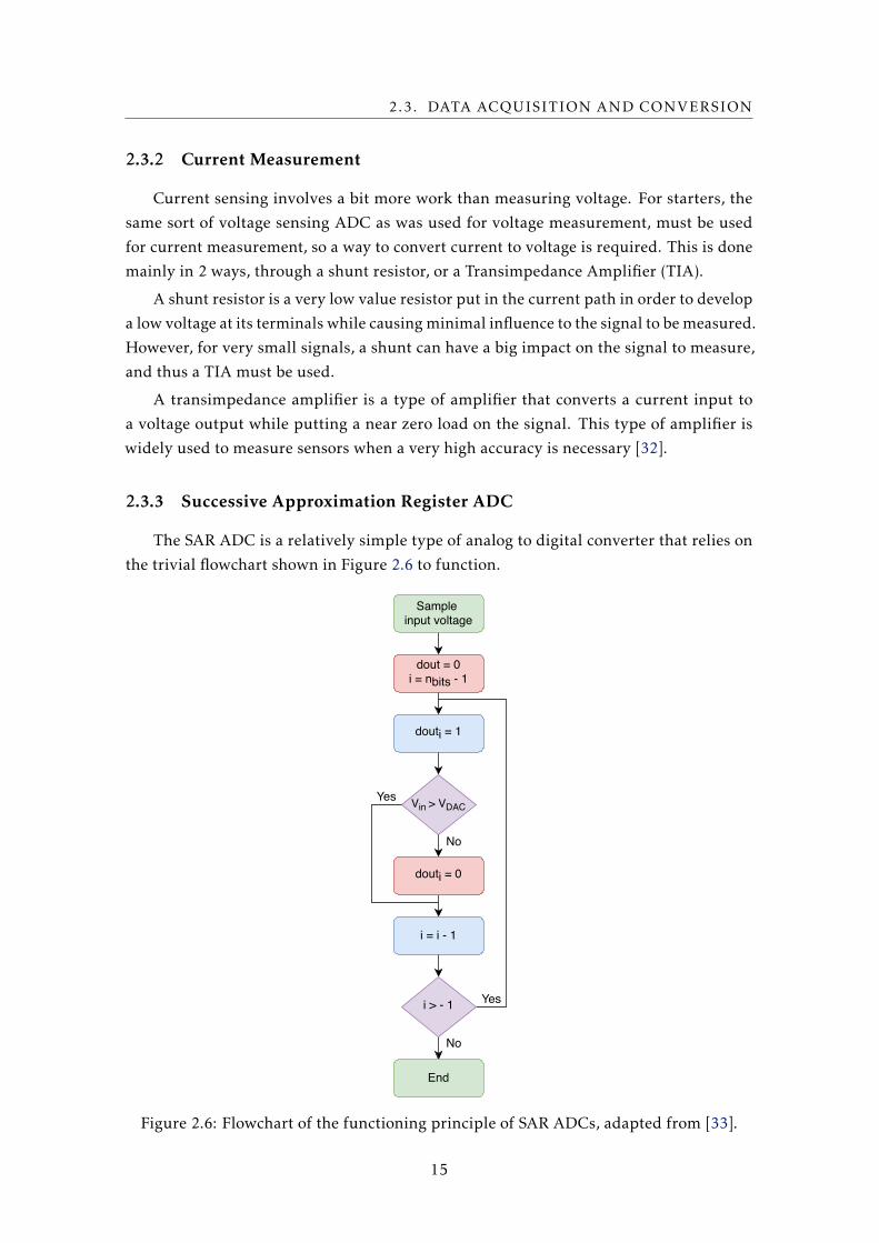
2.3.3 Successive Approximation Register ADC
The SAR ADC is a relatively simple type of analog to digital converter that relies on
the trivial flowchart shown in Figure 2.6 to function.
Sample input voltage
No
Yesi > - 1
End
dout = 0i = nbits - 1
douti = 1
Vin > VDACYes
douti = 0
i = i - 1
No
Figure 2.6: Flowchart of the functioning principle of SAR ADCs, adapted from [33].
15

CHAPTER 2. RESEARCH AND CONCEPT WORK
What this means in practice, is that the converter successively halves the conversion
scale in each iteration of the process and compares it to the signal, until it converges on
the value of the analog input. For each halving, an additional bit is calculated, so, for a 0.6
V signal, in a 1 V scale, the process would be as follows: Halve the initial scale, splitting
it in a 0 - 0.5 V range and a 0.5 - 1 V range. Comparing these halves to the analog signal,
we realize that the input is in the larger division, thus our Most Significant Bit (MSB) will
be 1. On the second iteration, the 0.5 - 1 V scale would be separated into 0.5 - 0.75 V
and 0.75 - 1 V ranges, where the signal would be in the smallest of the ranges, thus the
second bit would be zero. This processed would be repeated until a suitable resolution is
achieved, or the noise overpowers the signal and no more information can be extracted.
This is described in the flowchart on Figure 2.6, and a graphical representation of the
process can be seen in 2.7 [34].
0000000100100011010001010110011110001001101010111100110111101111
0 V
Full Scale
10
10
10
10
10
10
10
10
10
10
10
10
10
10
10
Figure 2.7: Graphical representation of the possible paths in a SAR ADC, adaptedfrom [34].
2.3.4 Delta-Sigma ADC
A Delta-Sigma or Sigma-Delta ADC, used interchangeably in this thesis, are cleverly
based around an "oversampling"architecture in order to simplify the input low pass filter,
shifting the noise spectrum beyond the passband. This means they can provide very good
performance, both in the form of resolution and accuracy.
The "oversampling"characteristic comes from the fact that, unlike standard converters
that operate at sampling frequencies close to the Nyquist frequency, the sampling in a
∆−Σ ADC is much higher than Nyquist, enabling a trade between conversion time and
resolution, which allows this type of converter to reach very high resolutions when driven
with a very high frequency clock [34].
The basic block architecture of the ∆−Σ ADC can be seen in Figure 2.8.
16
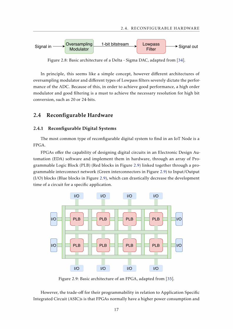
2.4. RECONFIGURABLE HARDWARE
OversamplingModulatorSignal in 1-bit bitstream Lowpass
Filter Signal out
Figure 2.8: Basic architecture of a Delta - Sigma DAC, adapted from [34].
In principle, this seems like a simple concept, however different architectures of
oversampling modulator and different types of Lowpass filters severely dictate the perfor-
mance of the ADC. Because of this, in order to achieve good performance, a high order
modulator and good filtering is a must to achieve the necessary resolution for high bit
conversion, such as 20 or 24-bits.
2.4 Reconfigurable Hardware
2.4.1 Reconfigurable Digital Systems
The most common type of reconfigurable digital system to find in an IoT Node is a
FPGA.
FPGAs offer the capability of designing digital circuits in an Electronic Design Au-
tomation (EDA) software and implement them in hardware, through an array of Pro-
grammable Logic Block (PLB) (Red blocks in Figure 2.9) linked together through a pro-
grammable interconnect network (Green interconnectors in Figure 2.9) to Input/Output
(I/O) blocks (Blue blocks in Figure 2.9), which can drastically decrease the development
time of a circuit for a specific application.
PLB PLB PLB PLB
PLB PLB PLB PLBI/O
I/O
I/O
I/O
I/O
I/O
I/O
I/O
I/O
I/O
I/O
I/O
Figure 2.9: Basic architecture of an FPGA, adapted from [35].
However, the trade-off for their programmability in relation to Application Specific
Integrated Circuit (ASIC)s is that FPGAs normally have a higher power consumption and
17
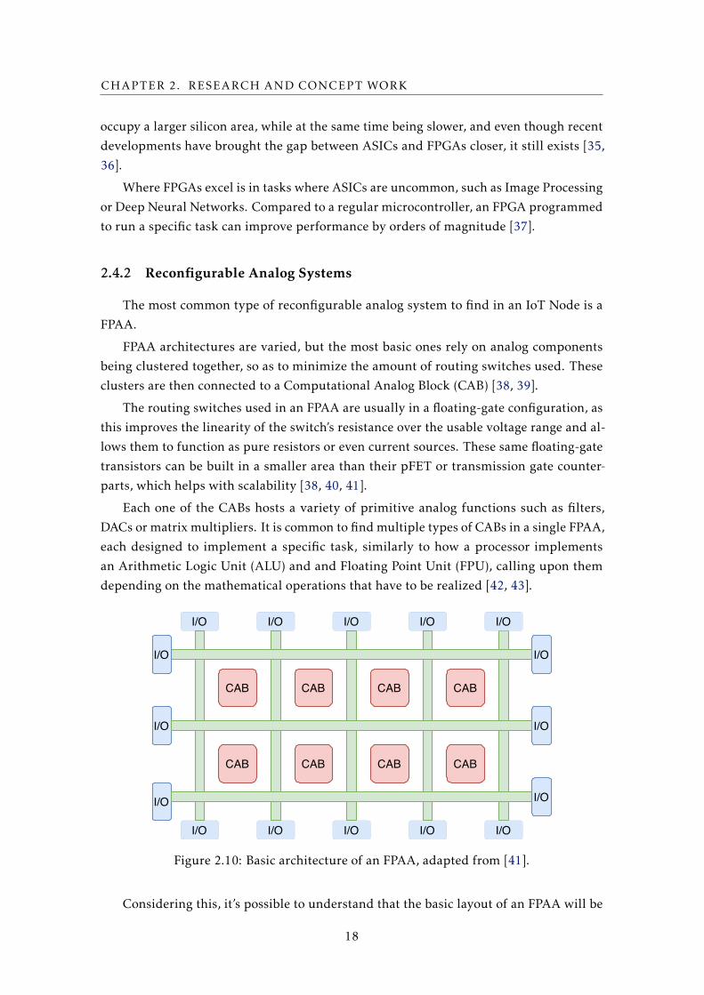
CHAPTER 2. RESEARCH AND CONCEPT WORK
occupy a larger silicon area, while at the same time being slower, and even though recent
developments have brought the gap between ASICs and FPGAs closer, it still exists [35,
36].
Where FPGAs excel is in tasks where ASICs are uncommon, such as Image Processing
or Deep Neural Networks. Compared to a regular microcontroller, an FPGA programmed
to run a specific task can improve performance by orders of magnitude [37].
2.4.2 Reconfigurable Analog Systems
The most common type of reconfigurable analog system to find in an IoT Node is a
FPAA.
FPAA architectures are varied, but the most basic ones rely on analog components
being clustered together, so as to minimize the amount of routing switches used. These
clusters are then connected to a Computational Analog Block (CAB) [38, 39].
The routing switches used in an FPAA are usually in a floating-gate configuration, as
this improves the linearity of the switch’s resistance over the usable voltage range and al-
lows them to function as pure resistors or even current sources. These same floating-gate
transistors can be built in a smaller area than their pFET or transmission gate counter-
parts, which helps with scalability [38, 40, 41].
Each one of the CABs hosts a variety of primitive analog functions such as filters,
DACs or matrix multipliers. It is common to find multiple types of CABs in a single FPAA,
each designed to implement a specific task, similarly to how a processor implements
an Arithmetic Logic Unit (ALU) and and Floating Point Unit (FPU), calling upon them
depending on the mathematical operations that have to be realized [42, 43].
CAB CAB CAB CAB
CAB CAB CAB CAB
I/O
I/O I/O
I/O
I/O
I/O
I/O
I/O
I/O
I/O
I/O
I/O
I/O
I/O
I/O
I/O
Figure 2.10: Basic architecture of an FPAA, adapted from [41].
Considering this, it’s possible to understand that the basic layout of an FPAA will be
18
2.5. EDGE COMPUTING
similar to that of an FPGA, where the PLBs will be replaced with CABs, as can be seen in
Figure 2.10.
In Figure 2.10, the Red Blocks represent CABs, the Green interconnectors represent
the routing switches, are the Blue Blocks represent the I/O connectors.
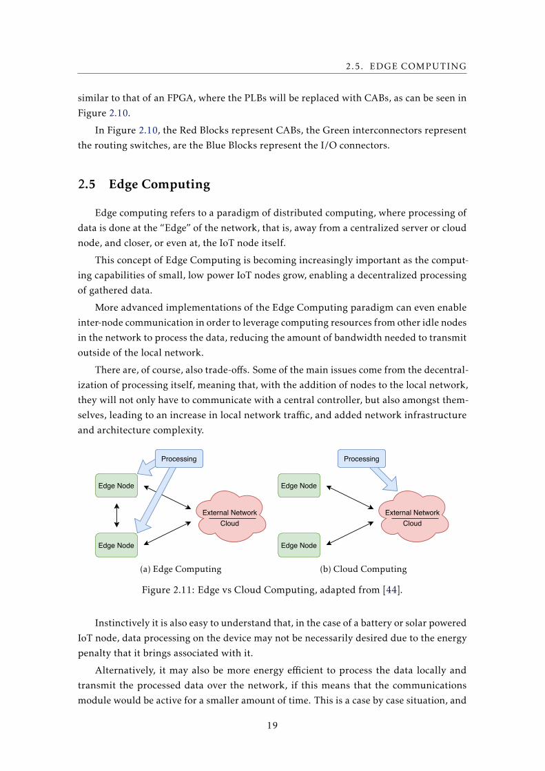
2.5 Edge Computing
Edge computing refers to a paradigm of distributed computing, where processing of
data is done at the “Edge” of the network, that is, away from a centralized server or cloud
node, and closer, or even at, the IoT node itself.
This concept of Edge Computing is becoming increasingly important as the comput-
ing capabilities of small, low power IoT nodes grow, enabling a decentralized processing
of gathered data.
More advanced implementations of the Edge Computing paradigm can even enable
inter-node communication in order to leverage computing resources from other idle nodes
in the network to process the data, reducing the amount of bandwidth needed to transmit
outside of the local network.
There are, of course, also trade-offs. Some of the main issues come from the decentral-
ization of processing itself, meaning that, with the addition of nodes to the local network,
they will not only have to communicate with a central controller, but also amongst them-
selves, leading to an increase in local network traffic, and added network infrastructure
and architecture complexity.
External Network
Cloud
Edge Node
Edge Node
Processing
(a) Edge Computing
External Network
Cloud
Edge Node
Edge Node
Processing
(b) Cloud Computing
Figure 2.11: Edge vs Cloud Computing, adapted from [44].
Instinctively it is also easy to understand that, in the case of a battery or solar powered
IoT node, data processing on the device may not be necessarily desired due to the energy
penalty that it brings associated with it.
Alternatively, it may also be more energy efficient to process the data locally and
transmit the processed data over the network, if this means that the communications
module would be active for a smaller amount of time. This is a case by case situation, and
19
CHAPTER 2. RESEARCH AND CONCEPT WORK
must be weighed when designing the IoT Node.
Another obvious trade-off is that, even with many nodes in a network, and the ability
to use idle nodes to process certain data, the computing power may not be enough for a
specific task, as such Edge Computing alone may not be able to fully fulfill the processing
requirements of the IoT system.
Because of this, it becomes apparent that Edge and Cloud Computing must definitely
coexist, and the choice of one over the other, or even a combination of both, depends on
the specific application at hand [44, 45].
2.6 Concept Work
The objective of this thesis work is to design and develop an advanced IoT Node, for
environmental sensing of several physical, chemical and biological parameters through
various sensors, with a high level of flexibility and reconfigurability, in order to accom-
modate the ability to digitize signals from each different sensor, in order to prepare them
for digital processing.
To achieve this with a very high level of precision, it is necessary to research, design,
implement and test an IoT Node based on a state-of-the-art SoC and Analog Front-End
(AFE), which can acquire the sensor signal and use advanced signal processing to extract
additional information from the acquired signals.
This, of course, always while holding under consideration the power requirements of
the system, as it may be deployed as a battery powered solution.
2.6.1 Design and Architecture
The architecture of the IoT Node is to be based around a PSoC 5LP or PSoC 6 repro-
grammable Microcontroller (µC) by Cypress.
Both µC options have their merits. The PSoC 5LP is based on a single Cortex®-M3
core, with a maximum clock speed of 80 MHz, and contains up to two 12-bit SAR ADC
and one 20-bit ∆−Σ ADC, 62 General Purpose I/O (GPIO) pins, with no built-in wireless
communication options.
However, the PSoC 6 uses a totally different dual-core architecture, based on the
combination of a Cortex®-M4 core and a Cortex®-M0+ core, with a clock of up to 150
MHz on the former and 100 MHz on the latter, providing much higher computing power
than the PSoC 5LP, however, it has only a single 12-bit SAR ADC, greatly reducing
the analog to digital conversion capabilities, on the other hand, it can have up to 102
GPIO pins, allowing for more connected devices, and can also have built-in BLE wireless
communication.
Aside from the main microcontroller, the IoT Node can, if necessary, contain a high
precision dedicated AFE module. The preliminary candidates are the ADuCM355 and
20

2.6. CONCEPT WORK
AD5941 by Analog Devices.
Both of these AFE modules contain high sampling rate 16-bit SAR ADCs, with the
ability to measure voltage, current and impedance, as well as having internal and external
current and voltage channels, ultralow leakage switch matrix, input Multiplexer (MUX),
input buffer and programmable gain amplifier. This means that in the analog input
section both these AFE modules are very similar, with the main difference being the
digital to analog conversion section, where the ADuCM355 has more capabilities, and in
the peripheral communication protocols, where the ADuCM355 can communicate using
I2C, UART and SPI while the AD5941 can only communicate using SPI.
(a) ADuCM355 Simplified Block Diagram
(b) AD5941 Simplified Block Diagram
Figure 2.12: Comparison of the simplified block diagram of the ADuCM355 and theAD5941 Analog Front-End (AFE) modules, obtained from the respective product datasheets, [46] and [47], respectively.
As a way to interface with several sensors, the analog inputs of either the PSoC micro-
controller or the AFE module must be multiplexed. Multiplexing allows a single analog
input to read multiple independent sensors, one at a time, through the control of the
multiplexing device.
The optimal characteristics to look for in a multiplexer are a large number of I/O ports,
to allow the interface of as many sensors as possible and a low ON Resistance (RON ), so
21
CHAPTER 2. RESEARCH AND CONCEPT WORK
as to alter the input signal as little as possible. Because of this, the primary multiplexer
being considered is the MAX14661 from Maxim [48]. This is a 16 input and 2 output
multiplexer, with a typical RON of 5.5 Ω. When controlled though an I2C interface, up
to 4 of these multiplexers can be used in a system, allowing for up to 32 independent
sensors to be connected, when using a 2-wire sensor. However, when controlled through
SPI, a virtually infinite number of multiplexers can be used, limited only by the number
of available SPI Slave Select pins which can be driven my the microcontroller.
2.6.2 Block Diagram for the Proposed Architecture
Using what we have previously researched in Section 2.1.1 and Section 2.6.1, we can
sketch up a preliminary block diagram for the architecture of the proposed IoT Node,
with the selected components. This can be seen in Figure 2.13, and contains some details
which are yet to be fully defined, such as the use of I2C or SPI communication to interface
with the multiplexers, as well as the number of multiplexers used.
Microcontroller:
Cypress PSoC 5LPCypress PSoC 6
Analog Front End:
ADuCM355AD5941
Power Management
Communication:
Bluetooth Low EnergyWi-FiNB-IoTLoRa
MAX14661
SensorsActuators
MAX14661
SensorsActuators
SensorsActuators
SensorsActuators
MAX14661SensorsActuators
MAX14661
SensorsActuators
SensorsActuators
SensorsActuators
Optional
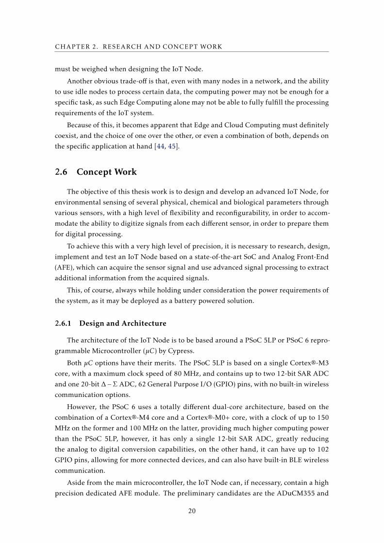
Figure 2.13: Block diagram of the proposed IoT Node.
Here we can see that the proposed IoT Node will allow the connection of a large
number of sensors through the cluster of multiplexers. These multiplexers are 16 input, 2
output MAX14661, enabling the ability to connect the sensors to either the AFE or to the
PSoC microcontroller directly, which means that the AFE module can be removed when
the application doesn’t demand a very high precision measurement.
2.6.3 Preliminary Testing
As a proof of concept for the proposed architecture in Section 2.6.2, a similar system
was tested in PSoC Creator, the Integrated Design Environment (IDE) Software used to
program Cyress’ PSoC microcontrollers. The tested system is very simple, and consists
of using a MUX with eight analog inputs and one analog output, connected to the ∆−ΣADC, which is configured for a 16-bit resolution. The signal read by the ADC is then sent
22
2.6. CONCEPT WORK
to the host computer through a UART Interface. A simple switch on the CY8CKIT-059
PSoC Prototyping Kit, which is being used for this testing, controls the switching of the
MUX’s channels.
The block diagram of the implemented test system can be seen below, in Figure 2.14,
and the code used to control this system can be found in Appendix A.
Figure 2.14: System implemented in PSoC Creator for testing.
This basic system tests the operating principles of the underlying proposal for the
final work. It uses the ∆−Σ ADC to read signals from eight inputs connected to a MUX,
and transmits the readings over a communication interface. The final work will function
in a similar fashion, with added complexity, of course, however the success in this test
proves that the concept work is sound.
23


Chapter
3Board Development
The third chapter of this thesis work deals with the process surrounding the develop-
ment of the IoT node’s Printer Circuit Board (PCB), first from a perspective of hardware
development and then from a perspective of software development, given that both com-
ponents are fundamental to the proper functioning of the noise, and will have to work
together in order to achieve the desired result.
Initially there is a description of the steps taken to develop the PCB in KiCad [49],
both in terms of the schematic design, as well as the circuit board layout itself, while also
including a brief description of finalized component selection and some of the decisions
that led to these choices. There is then a explanation of some of the considerations that
were had in the design of the PCB with regard to noise isolation and a brief summary
of the used ICs and their functions, followed by the experience when assembling all the
components on the board.
The software section describes how problems were tackled relating to the software
side of the IoT node, starting with the selection of analog sensor channels, then discussing
wired data transmission through the USBUART interface and some of the challenges faced
when reading sensor data from both the PSoC 5 LP microcontroller as well as the AD5941
AFE, specially as the latter one includes a very extensive library which needed to be
ported to the PSoC microcontroller, including some very good examples for the intended
use case of this IoT node as well.
25
CHAPTER 3. BOARD DEVELOPMENT
3.1 Hardware Development
The primary goal in terms of hardware development is to create a printed circuit
board with the components proposed in Section 3.1.1. This PCB must contain all the
described components, PSoC microprocessor, wireless communications, High Precision
Analog Front End and MAX14661 multiplexers, while providing adequate, clean power
to all of them, including some special care in terms of circuit grounding, in an attempt to
reduce noise in the sensor measurements.
The PCB was developed in KiCad, a free software suite that facilitates the design of
schematics for electronic circuits and their conversion into printed circuit boards, as well
as provide a 3D Viewer and the ability to export production oriented documents like Bills
of Materials and Gerber files.
Due to the relatively accessible pricing, a 4-layer type of PCB was chosen, this means
the circuit board has 4 independent copper layers in which tracks can be laid. This is
something that not only helps with layout of the traces and components due to more
available space, but also helps with grounding, as one or more of these layers can be used
as a dedicated ground plane.
1 2 3 4 5 6
1 2 3 4 5 6
A
B
C
D
A
B
C
D
Date: KiCad E.D.A. kicad (5.1.5)-3
Rev: Size: A4Id: 4/6
Title: File: IoT Sensor Node HPFE.schSheet: /IoT Sensor Node HPFE/
C24470nF
C20470nF
C25470nF
C22100nF
D2LED
RC0_21RC0_12RC0_03
VREF_2V54
AVDD_REG5
DVDD6
NC 7
VBIAS08
VZERO09
NC 10
XTALI 11
XTALO 12
DGND 13
DVDD_REG1V814
CS* 15SCLK 16MOSI 17MISO 18
GPIO0 19
GPIO1 20
GPIO2 21
RESET* 22
DGND 23
NC 24
DGND 25
IOVDD 26
AFE327
AFE428
AGND 29
AVDD30
VBIAS_CAP31
RCAL032
RCAL133
AFE134
AFE235
AIN3/BUF_VREF1V836AIN237AIN138AIN039
AIN4/LPF040
AVDD41
AGND 42VREF_1V8243
AGND_REF 44
SE045
DE046
CE047
RE048
EP 49
U3AD5941BCPZ
C161uF
C151uF
C23100nF
R210KR
C194.7uF
C21470nF
R200R
1234
J4Conn_01x04
R1200R
R190R
SW1RESET
123456
J3Conn_01x06
R31KR
FE_VREF_2V5
RESET
FE_AD5941_CS
FE_3V3
FE_VBIAS0
RESET
FE_VSS
FE_VSS
FE_3V3A
FE_VREF_1V82FE_DVDD_REG1V8FE_3V3FE_AVDD_REG
FE_VZERO0
FE_AIN1FE_AIN2FE_AIN3
FE_MOSI
RCAL1
FE_VSS
RCAL0
FE_VBIAS_CAP
FE_AIN0
FE_3V3A
FE_VSS
FE_SCLK
FE_MISO
FE_MOSI
FE_3V3
FE_VSSA
FE_VSSA
FE_VZERO0
FE_VSSFE_3V3
FE_VBIAS_CAP
FE_3V3
FE_3V3A
FE_AD5941_CSFE_SCLK
FE_MISO
RCAL1
RCAL0
FE_VSS
FE_VBIAS0
FE_VSSFE_VSS
FE_VSS
FE_VSSFE_VSSFE_VSSFE_VSS
FE_VSSFE_3V3
FE_VSSAFE_3V3A
FE_AVDD_REG
FE_AIN3
FE_AIN0FE_AIN1FE_AIN2
FE_VREF_1V82 FE_VREF_2V5
FE_DVDD_REG1V8
Vbias_cap
Vzero0 and Vbias
RCAL
DVDD 1.8V and AVDD
Signal Connector
AD5941
RCAL
HPFE 3.3V Decouple
Power + Data Connector
HPFE 3.3VA Decouple 1.82V and 2.5V
Status LED
Analog Planes
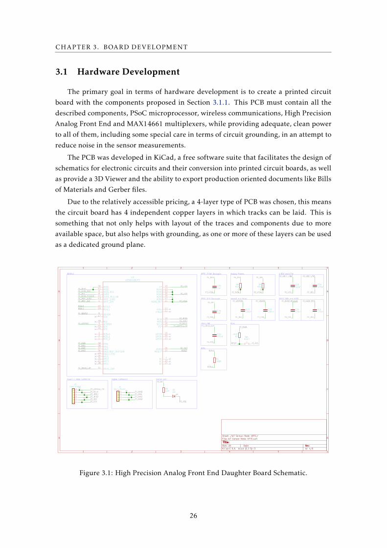
Figure 3.1: High Precision Analog Front End Daughter Board Schematic.
26

3.1. HARDWARE DEVELOPMENT
The first step of the PCB development is to create a schematic with the chosen compo-
nents and make the signal and power connections between them. This consists in having
a representation of the inputs and outputs of all the individual ICs and carefully choosing
which ports should be connected to which. Using the small AFE daughter board as an
example, a circuit schematic looks similar to what is represented in Figure 3.1. The full
circuit schematic and board layout for the developed node are available in Appendix B.
3.1.1 Final Component Selection
When it came to the final component selection, the choice for the main microcon-
troller was to use the PSoC 5LP, for three main reasons:
Firstly, the PSoC 6 microcontroller uses a Ball Grid Array (BGA) style package, mak-
ing it extremely difficult to solder on the PCB with the available soldering techniques,
while the PSoC 5LP uses a relatively simple Quad Flat Package (QFP) with 100 leads.
Secondly, the PSoC 5LP contains an internal 20-bit ∆−Σ ADC and two 12-bit SAR
ADC, while the PSoC 6 contains a single 12-bit SAR ADC, meaning that board perfor-
mance without the external AFE module should be higher with the PSoC 5LP.
Lastly, the QFP package of the PSoC 5LP allows for the separation of digital and
analog ground signals, something very important in order to reduce overall analog signal
noise, specially due to noise coming from digital interfaces, while the package on the
PSoC 6 wouldn’t allow such separation.
Another important decision was to use the AD5941 AFE module. This decision was
also mostly based on the IC package type, as the ADuCM355 uses the same BGA package
as the PSoC 6, which makes it virtually impossible to solder by hand or with conventional
reflow methods.
Cypress PSoC 5LPMicrocontroller
AD5941Analog Front End
Power Management
NB-IoT WirelessCommunications
UART WiredCommunications
MAX14661
SensorsActuators
MAX14661
SensorsActuators
SensorsActuators
SensorsActuators MAX14661
SensorsActuators
MAX14661
SensorsActuators
SensorsActuators
SensorsActuators
Optional
MAX14661
MAX14661
SensorsActuators
SensorsActuators
SensorsActuators
SensorsActuators
Figure 3.2: Finalized block diagram of the proposed IoT Node.
27
CHAPTER 3. BOARD DEVELOPMENT
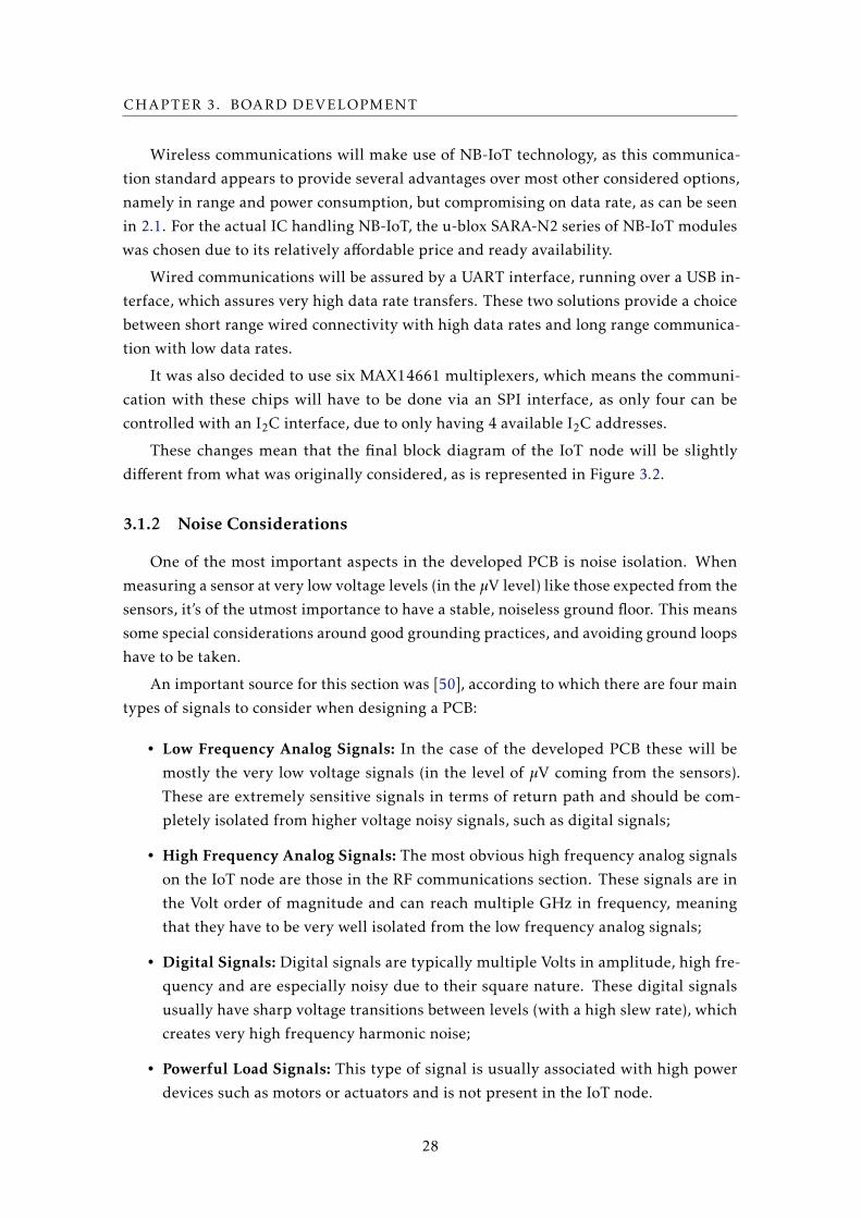
Wireless communications will make use of NB-IoT technology, as this communica-
tion standard appears to provide several advantages over most other considered options,
namely in range and power consumption, but compromising on data rate, as can be seen
in 2.1. For the actual IC handling NB-IoT, the u-blox SARA-N2 series of NB-IoT modules
was chosen due to its relatively affordable price and ready availability.
Wired communications will be assured by a UART interface, running over a USB in-
terface, which assures very high data rate transfers. These two solutions provide a choice
between short range wired connectivity with high data rates and long range communica-
tion with low data rates.
It was also decided to use six MAX14661 multiplexers, which means the communi-
cation with these chips will have to be done via an SPI interface, as only four can be
controlled with an I2C interface, due to only having 4 available I2C addresses.
These changes mean that the final block diagram of the IoT node will be slightly
different from what was originally considered, as is represented in Figure 3.2.
3.1.2 Noise Considerations
One of the most important aspects in the developed PCB is noise isolation. When
measuring a sensor at very low voltage levels (in the µV level) like those expected from the
sensors, it’s of the utmost importance to have a stable, noiseless ground floor. This means
some special considerations around good grounding practices, and avoiding ground loops
have to be taken.
An important source for this section was [50], according to which there are four main
types of signals to consider when designing a PCB:
• Low Frequency Analog Signals: In the case of the developed PCB these will be
mostly the very low voltage signals (in the level of µV coming from the sensors).
These are extremely sensitive signals in terms of return path and should be com-
pletely isolated from higher voltage noisy signals, such as digital signals;
• High Frequency Analog Signals: The most obvious high frequency analog signals
on the IoT node are those in the RF communications section. These signals are in
the Volt order of magnitude and can reach multiple GHz in frequency, meaning
that they have to be very well isolated from the low frequency analog signals;
• Digital Signals: Digital signals are typically multiple Volts in amplitude, high fre-
quency and are especially noisy due to their square nature. These digital signals
usually have sharp voltage transitions between levels (with a high slew rate), which
creates very high frequency harmonic noise;
• Powerful Load Signals: This type of signal is usually associated with high power
devices such as motors or actuators and is not present in the IoT node.
28

3.1. HARDWARE DEVELOPMENT
Only three of these four types of signals are present in the IoT node, which already
slightly simplifies the design process, however, mixing low frequency analog signals
with digital and high frequency analog signals still requires careful design considerations
around the ground return path and the routing of the low frequency, and low voltage
analog signals.
To achieve this, two separate ground planes were created, one for low frequency
analog signals (denominated Analog Ground), and one for digital and high frequency
ones (denominated Digital Ground). The digital ground plane was then virtually divided
in a pure digital section and a high speed analog section for RF signals.
Ultimately, the developed PCB had 2 separate ground planes, and 3 signal regions. At
the left is the Radio Frequency section, with the NB-IoT radio, antenna and SIM card slot.
In the center is the digital section with the PSoC microcontroller, power supply, wired
communications and the AD5941 AFE, and at the far right is the analog section, with the
6 multiplexers and all the analog sensor inputs.
The two ground planes are tied in a star ground configuration, with both planes
connected to the power supply ground in a single point, through a 0 Ω resistor. This is
the simplest way to isolate ground planes, however if this proves ineffective or insufficient,
a high frequency inductive filter such as a ferrite bead can be added.
Equally important to keep sensor noise as low as possible is the analog signal routing.
Even the best ground plane separation cannot help if the signals are routed poorly. To
achieve the best possible routing, all analog signals were routed only though the section
containing the analog ground plane for the trace running from the multiplexers into
the PSoC microcontroller and the AD5941 analog front end IC. These traces were also
made as wide as possible with the available space, in order to reduce signal loss to trace
resistance.
3.1.3 Radio Frequency Section
The radio frequency section is comprised of a u-blox SARA-N2 NB-IoT module. This
module provides NB-IoT communications in a relatively small, easy to integrate package
which is also priced reasonably, while only needing 3.3 V power, an antenna and a SIM
card to operate, but also offering some additional interfaces like UART and I2C in order
to control the sent and received data. This simplifies the integration of the module over
others that may need external 1.8 V power, or even external crystals or oscillators, as
these components are already integrated into the SARA-N2 module, as can be observed
in Figure 3.3.
The NB-IoT communication protocol is specifically designed for IoT applications, in
particular those which are battery operated, and thus conscious of energy consumption.
This translates to a communication standard which uses an extremely low amount of
energy and can communicate over large distances through the cellular network.
29
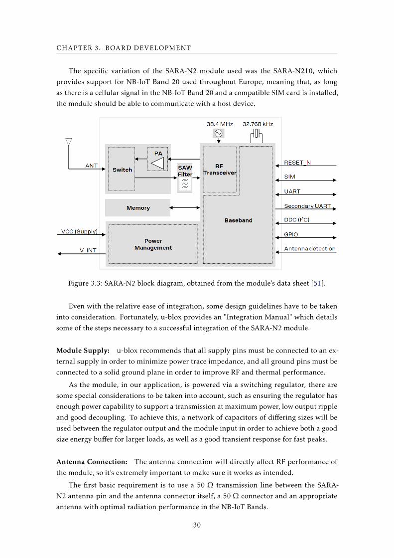
CHAPTER 3. BOARD DEVELOPMENT
The specific variation of the SARA-N2 module used was the SARA-N210, which
provides support for NB-IoT Band 20 used throughout Europe, meaning that, as long
as there is a cellular signal in the NB-IoT Band 20 and a compatible SIM card is installed,
the module should be able to communicate with a host device.
Figure 3.3: SARA-N2 block diagram, obtained from the module’s data sheet [51].
Even with the relative ease of integration, some design guidelines have to be taken
into consideration. Fortunately, u-blox provides an "Integration Manual" which details
some of the steps necessary to a successful integration of the SARA-N2 module.
Module Supply: u-blox recommends that all supply pins must be connected to an ex-
ternal supply in order to minimize power trace impedance, and all ground pins must be
connected to a solid ground plane in order to improve RF and thermal performance.
As the module, in our application, is powered via a switching regulator, there are
some special considerations to be taken into account, such as ensuring the regulator has
enough power capability to support a transmission at maximum power, low output ripple
and good decoupling. To achieve this, a network of capacitors of differing sizes will be
used between the regulator output and the module input in order to achieve both a good
size energy buffer for larger loads, as well as a good transient response for fast peaks.
Antenna Connection: The antenna connection will directly affect RF performance of
the module, so it’s extremely important to make sure it works as intended.
The first basic requirement is to use a 50 Ω transmission line between the SARA-
N2 antenna pin and the antenna connector itself, a 50 Ω connector and an appropriate
antenna with optimal radiation performance in the NB-IoT Bands.
30
3.1. HARDWARE DEVELOPMENT
In terms of the PCB design itself, a ground keep-out zone is advised, and no digital
signals should be routed near the RF connection as these can cause interference. The
50 Ω transmission line should be as short as possible in order to minimize insertion loss,
and it should have no stubs or cross with any other signals, so its placement is extremely
sensitive.
SIM Interface: SIM Card Interfacing is one of the least sensitive aspects of the PCB
design, from an RF perspective, however some mild considerations must still be taken
into account to prevent phenomena like RF coupling and electrostatic discharges.
To achieve this, the SIM Card connection lines must have ESD protection, as well
as small decoupling capacitors, specially as the SIM Card can be inserted and removed
during use. The SIM Card holder will also be placed near the SARA-N2 module just as
a general good design practice, in order to keep the data lines as short as possible and
board layout tidy.
System Functions: System functions are things such as Power On and Reset signals.
These signals must present adequate voltage levels to the SARA-N2 module and not have
any sorts of transient noise, which could compromise power up or reset the module during
operation.
Other Interfaces: Additional interfaces such as UART and I2C are essential to the op-
eration of the module, as they provide the data and control connection between the
SARA-N2 and the main microcontroller, which needs to receive and transmit information
through the NB-IoT wireless network. The SARA-N2 module in particular communi-
cates over UART with a 3.3V logic level, meaning that there is no need to do any sort of
voltage conversion as there is with other modules that operate at 1.8V, which the PSoC
microcontroller doesn’t support.
3.1.4 High Precision Analog Front End
The module which is designated as the High Precision Analog Front End is a small
daughter board that can be connected to the main IoT Node and has an AD5941 Analog
Front End IC which provides a DAC and ADC with a significantly higher resolution and
sample rate, while hopefully having a lower noise level, than those integrated into the
PSoC 5 LP microcontroller.
This additional module can be added to the main board when there is need for addi-
tional performance, as, while the ADC on the PSoC can have a higher 20-bit resolution, it
can only do so at an extremely low sample rate of 187 samples per second, while the ADC
on the AD5941 can achieve 16-bit at up to eight hundred thousand samples per second,
which is slightly higher.
31
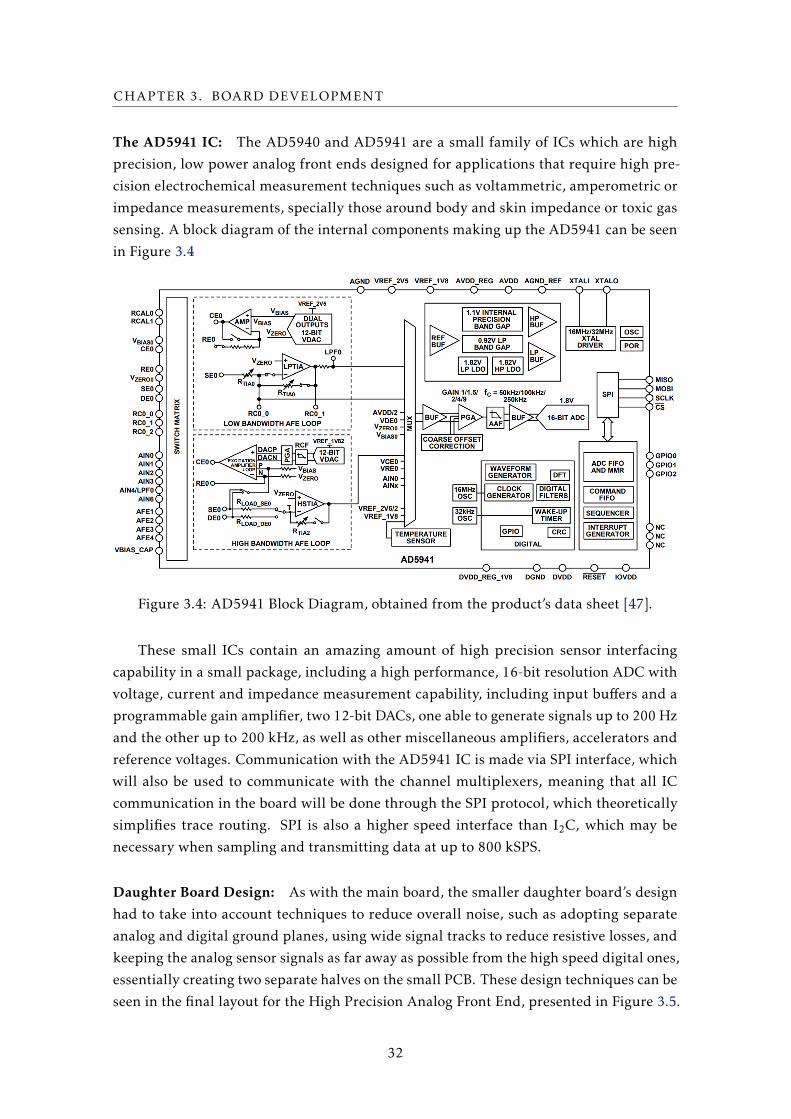
CHAPTER 3. BOARD DEVELOPMENT
The AD5941 IC: The AD5940 and AD5941 are a small family of ICs which are high
precision, low power analog front ends designed for applications that require high pre-
cision electrochemical measurement techniques such as voltammetric, amperometric or
impedance measurements, specially those around body and skin impedance or toxic gas
sensing. A block diagram of the internal components making up the AD5941 can be seen
in Figure 3.4
Figure 3.4: AD5941 Block Diagram, obtained from the product’s data sheet [47].
These small ICs contain an amazing amount of high precision sensor interfacing
capability in a small package, including a high performance, 16-bit resolution ADC with
voltage, current and impedance measurement capability, including input buffers and a
programmable gain amplifier, two 12-bit DACs, one able to generate signals up to 200 Hz
and the other up to 200 kHz, as well as other miscellaneous amplifiers, accelerators and
reference voltages. Communication with the AD5941 IC is made via SPI interface, which
will also be used to communicate with the channel multiplexers, meaning that all IC
communication in the board will be done through the SPI protocol, which theoretically
simplifies trace routing. SPI is also a higher speed interface than I2C, which may be
necessary when sampling and transmitting data at up to 800 kSPS.
Daughter Board Design: As with the main board, the smaller daughter board’s design
had to take into account techniques to reduce overall noise, such as adopting separate
analog and digital ground planes, using wide signal tracks to reduce resistive losses, and
keeping the analog sensor signals as far away as possible from the high speed digital ones,
essentially creating two separate halves on the small PCB. These design techniques can be
seen in the final layout for the High Precision Analog Front End, presented in Figure 3.5.
32
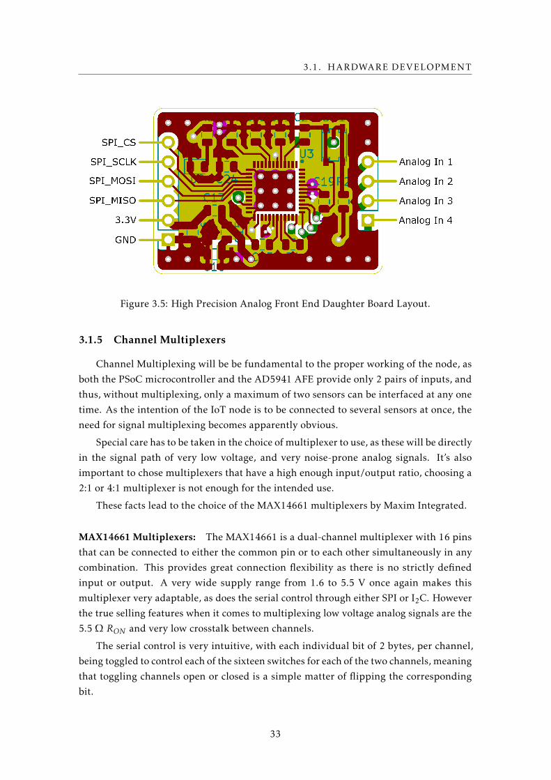
3.1. HARDWARE DEVELOPMENT
Figure 3.5: High Precision Analog Front End Daughter Board Layout.
3.1.5 Channel Multiplexers
Channel Multiplexing will be be fundamental to the proper working of the node, as
both the PSoC microcontroller and the AD5941 AFE provide only 2 pairs of inputs, and
thus, without multiplexing, only a maximum of two sensors can be interfaced at any one
time. As the intention of the IoT node is to be connected to several sensors at once, the
need for signal multiplexing becomes apparently obvious.
Special care has to be taken in the choice of multiplexer to use, as these will be directly
in the signal path of very low voltage, and very noise-prone analog signals. It’s also
important to chose multiplexers that have a high enough input/output ratio, choosing a
2:1 or 4:1 multiplexer is not enough for the intended use.
These facts lead to the choice of the MAX14661 multiplexers by Maxim Integrated.
MAX14661 Multiplexers: The MAX14661 is a dual-channel multiplexer with 16 pins
that can be connected to either the common pin or to each other simultaneously in any
combination. This provides great connection flexibility as there is no strictly defined
input or output. A very wide supply range from 1.6 to 5.5 V once again makes this
multiplexer very adaptable, as does the serial control through either SPI or I2C. However
the true selling features when it comes to multiplexing low voltage analog signals are the
5.5 Ω RON and very low crosstalk between channels.
The serial control is very intuitive, with each individual bit of 2 bytes, per channel,
being toggled to control each of the sixteen switches for each of the two channels, meaning
that toggling channels open or closed is a simple matter of flipping the corresponding
bit.
33
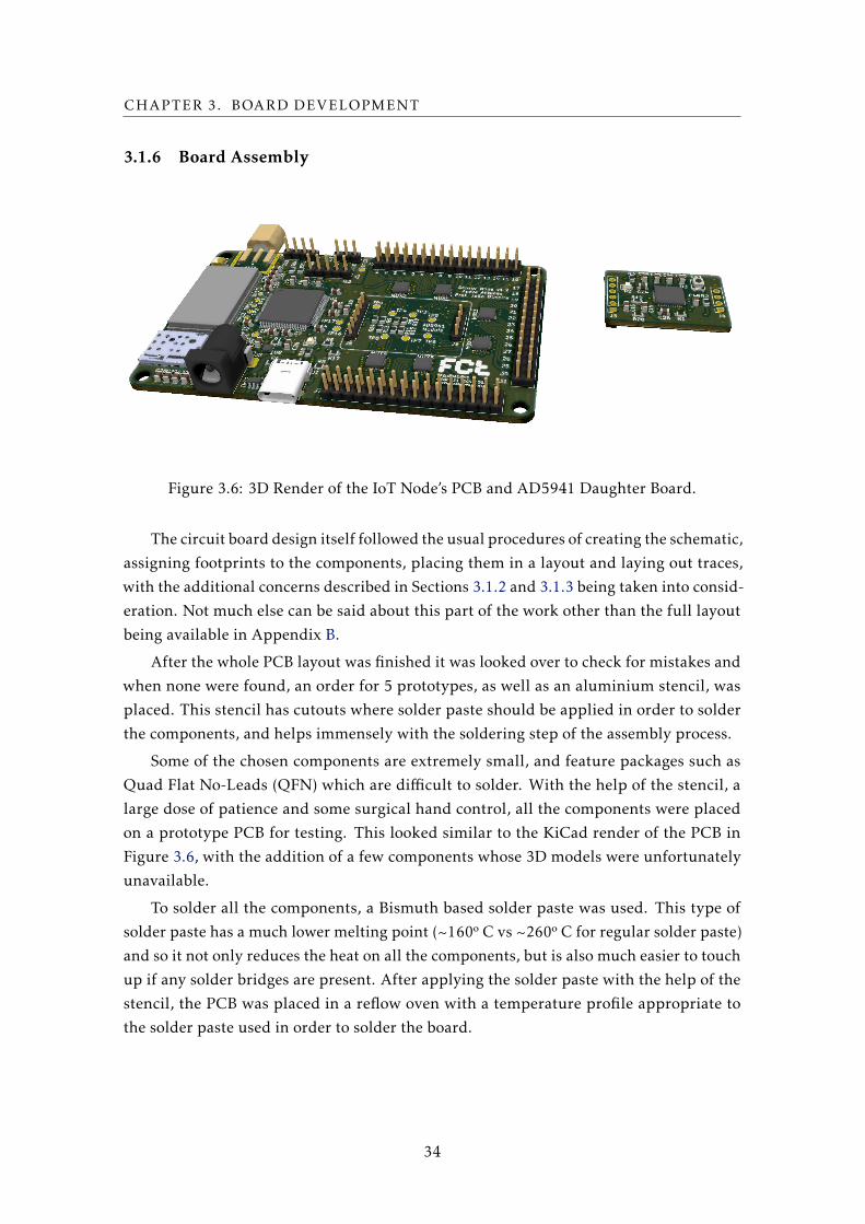
CHAPTER 3. BOARD DEVELOPMENT
3.1.6 Board Assembly
Figure 3.6: 3D Render of the IoT Node’s PCB and AD5941 Daughter Board.
The circuit board design itself followed the usual procedures of creating the schematic,
assigning footprints to the components, placing them in a layout and laying out traces,
with the additional concerns described in Sections 3.1.2 and 3.1.3 being taken into consid-
eration. Not much else can be said about this part of the work other than the full layout
being available in Appendix B.
After the whole PCB layout was finished it was looked over to check for mistakes and
when none were found, an order for 5 prototypes, as well as an aluminium stencil, was
placed. This stencil has cutouts where solder paste should be applied in order to solder
the components, and helps immensely with the soldering step of the assembly process.
Some of the chosen components are extremely small, and feature packages such as
Quad Flat No-Leads (QFN) which are difficult to solder. With the help of the stencil, a
large dose of patience and some surgical hand control, all the components were placed
on a prototype PCB for testing. This looked similar to the KiCad render of the PCB in
Figure 3.6, with the addition of a few components whose 3D models were unfortunately
unavailable.
To solder all the components, a Bismuth based solder paste was used. This type of
solder paste has a much lower melting point (~160º C vs ~260º C for regular solder paste)
and so it not only reduces the heat on all the components, but is also much easier to touch
up if any solder bridges are present. After applying the solder paste with the help of the
stencil, the PCB was placed in a reflow oven with a temperature profile appropriate to
the solder paste used in order to solder the board.
34

3.1. HARDWARE DEVELOPMENT
3.1.7 Power Consumption Considerations
Power consumption in any electronic device merits importance, however, when a
device is designed to be mostly battery operated, as is the case with the proposed IoT
node, power consumption becomes one of the most important parts of development, as
every small efficiency gain translates directly into longer battery life.
While no actual testing was conducted with the proposed node, a fair amount of
research was put into gaining a better understanding of the power consumption charac-
teristics of the PSoC 5LP microcontroller, including some power consumption reduction
techniques and the working principles of the available low power modes.
Luckily, Cypress provides detailed information into these subjects on Application
Note AN77900 [52], including not only extensive documentation about low power modes,
but also a spreadsheet which allows the user to estimate the power consumption for a
given use case and a PSoC Creator example project implementing some of the described
power consumption reduction techniques.
3.1.7.1 Power Modes
The PSoC 5LP has 4 main power modes: Active mode, AltAct mode, Sleep mode and
Hibernate mode. These power modes can be split into "active" modes and "low power"
modes. The available low power modes differ mainly in power consumption, wake-up
time and available wake-up sources, with a lower power consumption obviously leading
to a longer wake-up time and less available wake sources.
Active and AltAct modes: These are the main running modes of the PSoC microcon-
troller, with Active mode being the primary operating mode and AltAct an alternate
power configuration for Active mode. AltAct provides a method in which a set of analog
or digital blocks can be quickly turned off without the need to toggle each one individ-
ually. These are the modes that will be used when the microprocessor is doing any task
such as sensor sampling or data transmission.
Sleep mode: Sleep mode is the least severe of the two lower power modes available,
with a typical current consumption of 2 µA and a wake-up time of 25 µs, while also
providing the largest number of wake-up sources from the two low power modes. Sleep
mode can be entered by calling the CyPmCleep() function and the system can be woken
up from multiple sources including sleep timers, real-time clock, a button press or an
I2C command, among others.
Hibernate mode: Hibernate mode is the most severe low power mode and reduces cur-
rent consumption to a measly 300 nA while having a 125 µs wake-up time. Hibernate
35
CHAPTER 3. BOARD DEVELOPMENT
mode can be entered by calling the CyPmHibernate() function and it provides the small-
est amount of wake-up sources, being limited only to a button press, an over-temperature
event or a reset command.
These low power modes are extremely important in systems that have long pauses
between activities, such as the IoT node described in this dissertation, which can be
configured to have very long intervals between samples. For example, if the system is
configured to sample a sensor for 1 second, send the data, and then repeat the same
process a minute later, using the spreadsheet provided by Cypress in [52], the difference
between using sleep mode between samples, and running in active mode permanently is
a massive 20 to 30x decrease in overall power consumption.
Hibernate mode seems to be too extreme for the intended use, as the only methods of
waking the system back are to either physically press a button or to toggle the XRES pin
of the PSoC, both of which have to be physically controlled and mean that a person would
need to be present at all times to control data sampling, which is completely impractical
for the desired application.
There are some more considerations to have when reducing power consumption using
low power modes, for instance, by default the PSoC microcontrollers have a "Fast IMO
Startup" setting enabled, which starts the IMO with a 48 MHz clock in order to speed up
boot time, leading obviously to higher power consumption. Disabling this mode can be
useful when the system wakes up from sleep very often, as it reduces power consumption
during the wake from sleep phase.
Even so, not every single workload can use these low power modes. If continuous
sampling is required, or if PSoC has to be communicating with other devices, sleep mode
can’t be used, meaning that it’s also important to reduce active state power consumption
as much as possible.
3.1.7.2 Active Power Consumption Reduction
Reducing active state power consumption can be achieved in some very obvious ways
such as powering off unused components or running the microcontroller at a lower clock
speed, however, there are also some more obscure ways to achieve this effect and those
are the ones that will be explored.
Slowing Down the ADC: The Delta Sigma ADC on the PSoC microcontroller can be
configured anywhere from 8 to 20 bits of resolution, as well as a wide range of sampling
rates, however all of these factors affect the module’s power consumption. According
to [52], running the ADC at about half the maximum sample rate, at any resolution,
should result in a power consumption of around 0.8 µA, while running the ADC at the
maximum sample rate results in about 2.3 µA of power consumption.
36
3.1. HARDWARE DEVELOPMENT
Using Slow mode on the Current DAC: The PSoC 5LP has 4 DACs with both a voltage
and a current mode. For the drive of resistive sensors, the current mode is normally used
and the DACs allow for a "Slow" or "Fast" configuration. This setting basically dictates the
slew rate of the current, however, using the fast setting leads to a current consumption
which is about 10x higher than when using the slow mode. When driving slowly changing
sensors, the slow mode should be used to conserve energy.
Changing Clock Speeds According to Need: As it was stated in the introduction to
this section, one of the most obvious ways to reduce power consumption is to reduce
the clock speed of the system, however, this may not be possible due to the need for
higher clocks when processing data or when using a communications interface such as
USB. However, the PSoC microcontroller allows the dynamic change of clocks in code
through functions such as CyIMO_SetFrequency() which means that the clock can be
manipulated according to need, being set higher when it needs to be, and much lower
when the system is doing more routing tasks such as sampling sensors.
Lowering the Voltage: According to the spreadsheet provided by Cypress to calculate
the power consumption of the PSoC microcontrollers, the drawn current doesn’t change
with the supply voltage, and the PSoC accepts an input from 1.8 to 5 V. By lowering the
input voltage and maintaining the current, there is a drop in power consumption directly
proportional to the voltage drop.
Additionally there are "Low-Power" modes for several system components such as the
external crystal oscillator, GPIO pins, SIO pins, Digital Blocks and VREF Sources. While
these don’t have a very big impact in overall power consumption, it’s important to note
that these modes are still available.
3.1.7.3 High Power Consumption Components
From the previously mentioned spreadsheet it’s also easy to understand that some
components have a severe effect in power consumption, for instance, while the IMO clock
can be changed from 3 to 48 MHz while only incurring a 600 µA penalty, doing this same
change for the actual CPU clock results in a 20 mA jump to current usage.
Similarly, when using the USB interface, it is important to suspend communications
when they are not being used, as simply keeping an open communication line draws
10 mA of current.
37

CHAPTER 3. BOARD DEVELOPMENT
3.2 Software Development
As with any project involving a microcontroller, software needs to be developed in
order to achieve the designed tasks. This envelops everything from basic things like
selecting which internal features of the microcontroller to enable and define which ports
are connected, to more complex things like developing libraries to interact with external
ICs.
In the case of the chosen PSoC 5 LP microcontroller, this software development is
done through the PSoC Creator IDE.
3.2.1 PSoC Creator
PSoC Creator is an integrated development environment designed by Cypress that
enables software development, compiling and debugging for the PSoC architecture. The
IDE provides a graphical user interface which aids development.
There are essentially 5 main windows which will be used throughout this work.
Top Design: This first window provides an overview of "Components", internal features
of the PSoC microcontroller which can be picked from a list and subsequently enabled
and configured with the help of a graphical interface. This forms a sort of block diagram
of the developed system, where wire connections can be made between the different
components, such as connecting pins to ADCs or enabling interrupts and communication
interfaces.
This type of programming is extremely beginner friendly and was appreciated in a
first contact situation with the PSoC ecosystem.
A screenshot of the "Top Design" page for the developed software architecture can be
seen in Figure 3.7
Figure 3.7: Block Diagram on the "Top Design" Window of PSoC Creator.
Pins: The "Pins" window is rather self explanatory. It allows manual definition of where
each pin and component defined in the "Top Design" window should be physically con-
nected in the PSoC microcontroller.
38
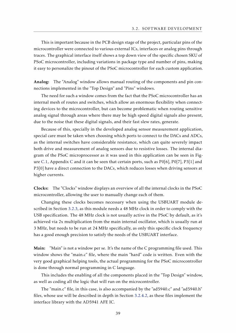
3.2. SOFTWARE DEVELOPMENT
This is important because in the PCB design stage of the project, particular pins of the
microcontroller were connected to various external ICs, interfaces or analog pins through
traces. The graphical interface itself shows a top down view of the specific chosen SKU of
PSoC microcontroller, including variations in package type and number of pins, making
it easy to personalize the pinout of the PSoC microcontroller for each custom application.
Analog: The "Analog" window allows manual routing of the components and pin con-
nections implemented in the "Top Design" and "Pins" windows.
The need for such a window comes from the fact that the PSoC microcontroller has an
internal mesh of routes and switches, which allow an enormous flexibility when connect-
ing devices to the microcontroller, but can become problematic when routing sensitive
analog signal through areas where there may be high speed digital signals also present,
due to the noise that these digital signals, and their fast slew rates, generate.
Because of this, specially in the developed analog sensor measurement application,
special care must be taken when choosing which ports to connect to the DACs and ADCs,
as the internal switches have considerable resistance, which can quite severely impact
both drive and measurement of analog sensors due to resistive losses. The internal dia-
gram of the PSoC microprocessor as it was used in this application can be seen in Fig-
ure C.1, Appendix C and it can be seen that certain ports, such as P0[6], P0[7], P3[1] and
P3[0] have a direct connection to the DACs, which reduces losses when driving sensors at
higher currents.
Clocks: The "Clocks" window displays an overview of all the internal clocks in the PSoC
microcontroller, allowing the user to manually change each of them.
Changing these clocks becomes necessary when using the USBUART module de-
scribed in Section 3.2.3, as this module needs a 48 MHz clock in order to comply with the
USB specification. The 48 MHz clock is not usually active in the PSoC by default, as it’s
achieved via 2x multiplication from the main internal oscillator, which is usually run at
3 MHz, but needs to be run at 24 MHz specifically, as only this specific clock frequency
has a good enough precision to satisfy the needs of the USBUART interface.
Main: "Main" is not a window per se. It’s the name of the C programming file used. This
window shows the "main.c" file, where the main "hard" code is written. Even with the
very good graphical helping tools, the actual programming for the PSoC microcontroller
is done through normal programming in C language.
This includes the enabling of all the components placed in the "Top Design" window,
as well as coding all the logic that will run on the microcontroller.
The "main.c" file, in this case, is also accompanied by the "ad5940.c" and "ad5940.h"
files, whose use will be described in depth in Section 3.2.4.2, as these files implement the
interface library with the AD5941 AFE IC.
39

CHAPTER 3. BOARD DEVELOPMENT
3.2.2 Analog Channel Selection
To select which analog signal to measure, an SPI command has to be sent to the
multiplexers instructing them to enable the specific sensor port to open, and whether to
route it to the PSoC microcontroller or the AD5941 AFE.
In the hardware design, the common port A of multiplexers 1, 2, 3 and 4 were con-
nected directly to the PSoC microcontroller in ports P0[6], P0[7], P3[1] and P3[0] as these
have a direct connection to the sensor driving DACs. The common port A of multiplexers
5 and 6 were left unconnected, leaving only common port B of each of these connected to
port 16 of multiplexers 4 and 3, respectively. Common port B of multiplexers 1 through
4 were connected directly to the input ports of the AD5941 AFE.
This meant that, to simply connect to a specific sensor port, specially those in multi-
plexers 5 and 6, some juggling of the open ports had to be done, as for instance, a port
connected to multiplexer 5 has to then travel to multiplexer 4 and only then to the PSoC
microcontroller or the AD5941 AFE.
The MAX14661 multiplexers are controlled either through I2C or SPI, however in
I2C mode they are limited to four separate addresses, meaning that a maximum of four
multiplexers can be used, which is why the developed board uses SPI to communicate
with these multiplexers. Port open and close is controlled through a series of four byte
long registers. In the developed analog channel selection function, each of these four
bytes is declared as a variable, with one set of four variables per pair of multiplexers, as
these will be controlled in pairs due to the minimum two-wire connection to sensors.
In total the PCB will have 47 analog channels, sixteen from each pair of multiplexers,
minus one from multiplexers 3 and 4 which serves as pass-through for multiplexers 5
and 6.
The function developed for easy control of channel opening and closing works through
a very simple principle, it takes three input variables: channel; output; state. Channel
corresponds to what analog channel is being addressed, output refers to the common pin
A or B, one connected to the PSoC, the other to the AD5941 and finally state indicates if
the intended action is to open or close the specific channel. There are 12 integer variables
which correspond to each of the bytes on the three pairs of multiplexers, when an open
command is called, the corresponding byte in these variables is changed and is trans-
mitted through SPI to the corresponding multiplexer. The same happens when a close
command is given.
3.2.3 USBUART Transmit and Receive
UART is the main wired communication method used. The PSoC microcontroller
offers two distinct methods of implementing UART interfaces, the first one is as a stan-
dalone interface, with the usual TX and RX lines, which will then connect to any other
40
3.2. SOFTWARE DEVELOPMENT
UART device. The second method is through a USBUART, that is, a UART interface run-
ning through the USB communication protocol. The PSoC Creator IDE has a template for
the USBFS (USB Full Speed) interface with all the descriptors implemented in order to
enumerate a simple serial port device. This second method is the one that will be used, as
the node is already powered via USB from a computer, and to transmit the UART data to
USB manually, an additional UART to USB converter IC would be needed, which would
add additional unnecessary complexity.
Two UART related functions were developed, one of them is a simple initialization
which configures the USBUART device with the setting of an incoming connection, mak-
ing it possible for the connected computer to use any Baud Rate, Parity or Polarity settings
and the PSoC will adapt to the settings used. The second one is a "bounce back" function
which simply reads what the connected computer wrote in the serial port and returns it.
This was done as a way to test two way communication functionality, even tho only one
way communication, from the PSoC to the serial port, was then used. A function for the
actual data transmission wasn’t developed, as there is already a function of the USBUART
module which implements the transmission of a string in a single command, after the
initialization process is done, making an extra function for this situation unnecessary.
3.2.4 Sensor Data Acquisition
As the ultimate purpose of the developed IoT node is to measure sensor data, this
is probably the most important part of the software development. Sensor data can be
acquired from two separate sources, either from the internal ADC on the PSoC microcon-
troller or from the external AD5941 AFE.
3.2.4.1 Sensor Data Acquisition from PSoC
The PSoC microcontroller has two types of internal ADC. The first type is a 12-bit
resolution, SAR ADC with an extremely fast sample rate of 1 million samples per second.
The advantage of this type of ADC is obvious, it has an extremely fast sample rate, which
is fundamental for fast changing signals, however it also has a relatively limited 12-bit
resolution which is not the perfect fit for high precision measurements. The second
type of internal ADC is a 20-bit resolution Delta Sigma converter, which, at full 20-bit
resolution has a sampling rate up to 187 samples per second, a far cry away from the 1
million samples of the SAR ADC.
For the intended application, however, the ∆−Σ ADC is clearly better suited, as there
can be a trade-off between sampling rate and resolution, whose optimal point will be
searched for in Section 4.2.
A large part of the software configuration of the ∆−Σ ADC is done through the
"Top Design" component, with an easy to use graphical interface that allows the user
to selecting things like Conversion Mode, Resolution, Conversion rate, Single Ended or
41
CHAPTER 3. BOARD DEVELOPMENT
Differential modes, Reference voltage and Input Range. This configuration window is
shown in Figure 3.8.
Figure 3.8: Configuration Page of the Delta-Sigma ADC in PSoC Creator.
As far as actual programming is concerned, very little has to be done apart from en-
abling the module through a single line of code and starting and stopping the conversion
when desired. Additionally, the PSoC Creator IDE makes available to the user precon-
figured functions which convert the ADC’s output code directly into volts, millivolts or
microvolts, which makes measurements extremely convenient.
3.2.4.2 Sensor Data Acquisition from AD5941
Communication with the AD5941 Analog Front End IC is made through an SPI con-
nection. This IC has an extremely extensive feature set and very powerful capabilities,
looking at the datasheet of these devices, we can attest that they have over 180 control
registers, which means that developing a library to control all their functionality every
time someone had the intention to integrate it into a custom design would be quite
complicated. Exactly because of this, Analog Devices provides an extensive firmware
library for the AD5940, AD5941 and ADuCM355 ICs. These are state-of-the-art SoC for
42
3.2. SOFTWARE DEVELOPMENT
electrochemical and biosensors, exactly the use case of the developed IoT node.
Porting this library is also made very simple by Analog Devices, as only six functions
have to be implemented: CS Set, CS Clear, RESET Set, RESET Clear, Delay 10 µs) and SPI
Read/Write N Bytes. Even tho they are simple, they present an issue, as the RESET pin
of the AD5941 is a push button control, luckily this function is only used as a hardware
reset of the AD5941 before the library is started, to ensure that the AD5941 is in a default
state when communication starts, which shouldn’t be an issue if the library is loaded right
after the IoT node is powered up. For a future version of the IoT node, however, AD5941
RESET functionality should be implemented.
Another peculiarity of the PSoC microcontroller is that it doesn’t allow manual con-
trol of the CS pin, this is instead done automatically by the SPI Transmit and Receive
functions, however the control of CS pin implemented by these functions matches what
is done in the AD5941 library, so this shouldn’t present an issue either.
To help guide the user of the AD5941, Analog Devices also provides an extensive
repository of example code for specific types of sensor measurement such as Amperomet-
ric, Impedance, Body Impedance, Temperature, etc. As well as some examples of sensor
polarization techniques such as square wave voltammetry. All in all, both the library and
the example files are extremely powerful in helping the user of the AD5941 get familiar
with the device.
In these examples, there is also an SPI Debug function which tests the SPI Writes and
Reads to the AD5941 which will be used in Chapter 4.4.
43


Chapter
4Board Testing
As with any sort of work, and especially development work, proper testing has to be
done in order to ensure the correct working order of all the different components, be they
hardware or software.
To that extent, several functional blocks of the developed PCB will be tested, starting
with the six MAX14661 Multiplexers, then moving on to the PSoC’s internal ∆−Σ ADC,
which also includes the PSoC’s internal current DAC, used to drive the device under test.
Finally, there is a small section about the tests made to the AD5941 AFE IC.
Figure 4.1: Picture of the assembled IoT Node and AD5941 Daughter Board.
45
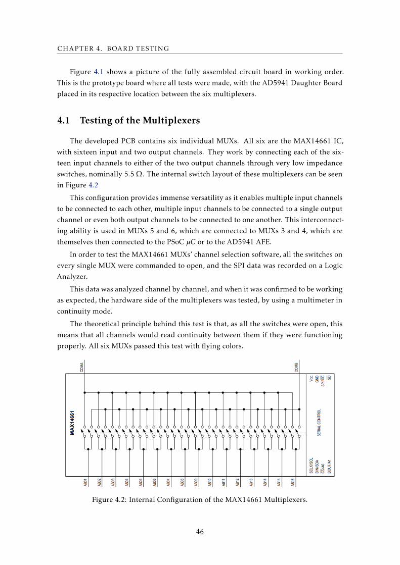
CHAPTER 4. BOARD TESTING
Figure 4.1 shows a picture of the fully assembled circuit board in working order.
This is the prototype board where all tests were made, with the AD5941 Daughter Board
placed in its respective location between the six multiplexers.
4.1 Testing of the Multiplexers
The developed PCB contains six individual MUXs. All six are the MAX14661 IC,
with sixteen input and two output channels. They work by connecting each of the six-
teen input channels to either of the two output channels through very low impedance
switches, nominally 5.5 Ω. The internal switch layout of these multiplexers can be seen
in Figure 4.2
This configuration provides immense versatility as it enables multiple input channels
to be connected to each other, multiple input channels to be connected to a single output
channel or even both output channels to be connected to one another. This interconnect-
ing ability is used in MUXs 5 and 6, which are connected to MUXs 3 and 4, which are
themselves then connected to the PSoC µC or to the AD5941 AFE.
In order to test the MAX14661 MUXs’ channel selection software, all the switches on
every single MUX were commanded to open, and the SPI data was recorded on a Logic
Analyzer.
This data was analyzed channel by channel, and when it was confirmed to be working
as expected, the hardware side of the multiplexers was tested, by using a multimeter in
continuity mode.
The theoretical principle behind this test is that, as all the switches were open, this
means that all channels would read continuity between them if they were functioning
properly. All six MUXs passed this test with flying colors.
Figure 4.2: Internal Configuration of the MAX14661 Multiplexers.
46

4.2. TESTING THE INTERNAL DELTA-SIGMA ADC WITH LOW VALUE
RESISTORS
4.2 Testing the Internal Delta-Sigma ADC with Low Value
Resistors
Testing the PSoC’s internal ∆−Σ ADC will be more difficult than the simple testing
done with the MUXs, as the ADC features many settings which can greatly affect the
output result.
In this testing we are looking at obtaining high accuracy measurements with the
lowest possible noise while keeping a reasonable sample rate. Unfortunately, as with all
things a trade-off has to be made between accuracy and sample rate. Higher resolution
modes result in a higher measurement accuracy and lower noise, however that also means
a lower sample rate, which may become a problem with fast changing signals or impact
the ability to apply certain filters.
Four different resolutions will be tested: 20, 18, 16 and 14 Bits. For each of these
resolutions there will be two test settings, one with a unitary input buffer gain, and one
with a buffer gain of 2. This brings the total to 8 test configurations. All tests will be made
in "Multi Sample (Turbo)" mode, with a 0 to VREF scale. This mode provides a higher
sample rate than the regular "Multi Sample" mode, although not quite reaching the rate
of "Continuous" mode.
For each configuration there are two main things to look at: measured value accuracy
and measurement noise.
The measured value will be represented by a bar graph with a 95% Confidence Inter-
val (CI) error bar. Each resolution and buffer gain combination will test three different
sensor polarization currents (1, 10 and 100 µA) and three different resistor values: 22 Ω
(measured with a multimeter as 21.7 Ω), 470 Ω (measured as 465 Ω) and finally 1 kΩ
(measured as 992 Ω).
The measurement noise will be displayed in table form for all the same scenarios,
three currents and three resistances, and the noise will be displayed in four different
forms:
• Peak to Peak Noise: Simple peak to peak determined by subtracting the lowest
measured value from the highest one.
• 99.7% Noise: Equivalent to 6σ or 6 standard deviations, the measured values closely
follow a normal distribution, thus a mean and standard deviation can be calculates.
• Root Mean Square (RMS) Noise: Equivalent to a single standard deviation, as we
can assume that the mean noise value is zero.
• RMS Noise (LSB): Regular RMS noise given as a function of least significant bits.
Graphs were generated by exporting the measured ADC value, already converted
to µV, through a UART interface running on USB. For each test, 5000 to 20000 mea-
surements were made. This data was then processed with a MATLAB script available in
Appendix D, noise values were calculated, and the shown graphs were plotted.
47

CHAPTER 4. BOARD TESTING
4.2.1 20-Bit Mode
Starting with the highest resolution mode available in the ∆−Σ ADC, 20-bit.
20-Bit, Buffer Gain = 2: The first test with a buffer gain of 2 and a sample rate of
92 samples per second exemplifies the most extreme end of the accuracy - sample rate
spectrum and represents a Least Significant Bit (LSB) value of 0.5 µA. Measurement
accuracy data is presented in Figure 4.3.
20-bit DelSig ADC, Multi Sample (Turbo), SR = 92 SPS, Buf. Gain = 2, 5.000 Samples per Measurement
22 Resistor
(Measured at 21.7 )
1 10 100
Polarization Current (A)
0
5
10
15
20
25
30
35
40
45
50
Me
asu
red
Re
sis
tor
Va
lue
()
470 Resistor
(Measured at 465 )
1 10 100
Polarization Current (A)
0
100
200
300
400
500
600
Me
asu
red
Re
sis
tor
Va
lue
()
1K Resistor
(Measured at 992 )
1 10 100
Polarization Current (A)
0
200
400
600
800
1000
1200
Me
asu
red
Re
sis
tor
Va
lue
()
Figure 4.3: Results of measurements using 20-bit ∆−Σ, Multi Sample (Turbo), SR = 92SPS, Buf. Gain = 2, 5.000 Samples per Measurement.
For these test parameters, measurement noise data is shown below, in Table 4.1, using
the four metrics described in Section 4.2.
Table 4.1: Noise values of measurements using 20-bit ∆−Σ, Multi Sample (Turbo), SR =92 SPS, Buf. Gain = 2, 5.000 Samples per Measurement.
Pol. Current (µA) 1 10 100Resistor Value(Ω) 22 465 992 22 465 992 22 465 992Noise pk-pk (µV) 9 9 11 10 14 17 55 106 140Noise 99.7% (µV) 7.94 8.27 10.2 9.0 11.8 14.3 46.2 85.0 108RMS Noise (µV) 1.32 1.38 1.70 1.50 1.96 2.37 7.71 14.2 18.0
RMS Noise (LSB) 2.71 2.82 3.49 3.08 4.02 4.86 15.8 29.0 36.8
48
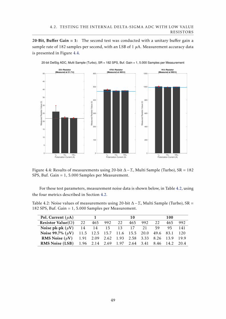
4.2. TESTING THE INTERNAL DELTA-SIGMA ADC WITH LOW VALUE
RESISTORS
20-Bit, Buffer Gain = 1: The second test was conducted with a unitary buffer gain a
sample rate of 182 samples per second, with an LSB of 1 µA. Measurement accuracy data
is presented in Figure 4.4.
20-bit DelSig ADC, Multi Sample (Turbo), SR = 182 SPS, Buf. Gain = 1, 5.000 Samples per Measurement
22 Resistor
(Measured at 21.7 )
1 10 100
Polarization Current (A)
0
5
10
15
20
25
30
35
40
45
50
Me
asu
red
Re
sis
tor
Va
lue
()
470 Resistor
(Measured at 465 )
1 10 100
Polarization Current (A)
0
100
200
300
400
500
600
Me
asu
red
Re
sis
tor
Va
lue
()
1K Resistor
(Measured at 992 )
1 10 100
Polarization Current (A)
0
200
400
600
800
1000
1200
Me
asu
red
Re
sis
tor
Va
lue
()
Figure 4.4: Results of measurements using 20-bit ∆−Σ, Multi Sample (Turbo), SR = 182SPS, Buf. Gain = 1, 5.000 Samples per Measurement.
For these test parameters, measurement noise data is shown below, in Table 4.2, using
the four metrics described in Section 4.2.
Table 4.2: Noise values of measurements using 20-bit ∆−Σ, Multi Sample (Turbo), SR =182 SPS, Buf. Gain = 1, 5.000 Samples per Measurement.
Pol. Current (µA) 1 10 100Resistor Value(Ω) 22 465 992 22 465 992 22 465 992Noise pk-pk (µV) 14 14 15 13 17 21 59 95 141Noise 99.7% (µV) 11.5 12.5 15.7 11.6 15.5 20.0 49.6 83.1 120RMS Noise (µV) 1.91 2.09 2.62 1.93 2.58 3.33 8.26 13.9 19.9
RMS Noise (LSB) 1.96 2.14 2.69 1.97 2.64 3.41 8.46 14.2 20.4
49
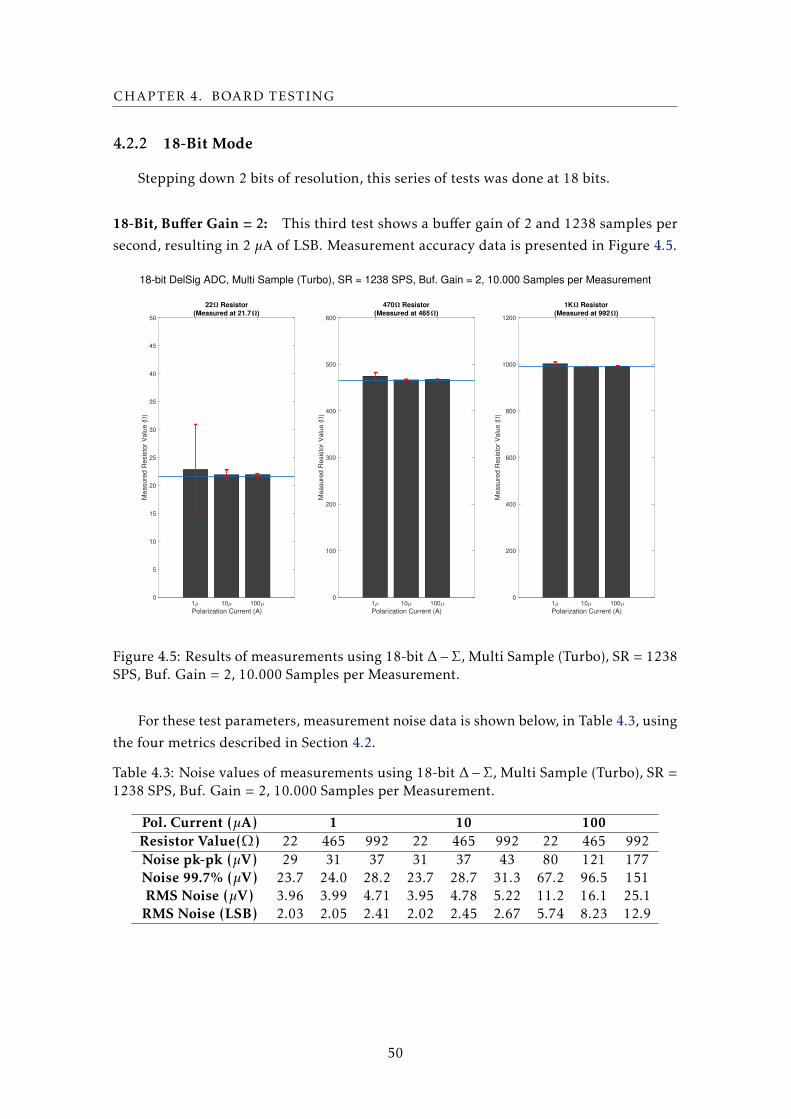
CHAPTER 4. BOARD TESTING
4.2.2 18-Bit Mode
Stepping down 2 bits of resolution, this series of tests was done at 18 bits.
18-Bit, Buffer Gain = 2: This third test shows a buffer gain of 2 and 1238 samples per
second, resulting in 2 µA of LSB. Measurement accuracy data is presented in Figure 4.5.
18-bit DelSig ADC, Multi Sample (Turbo), SR = 1238 SPS, Buf. Gain = 2, 10.000 Samples per Measurement
22 Resistor
(Measured at 21.7 )
1 10 100
Polarization Current (A)
0
5
10
15
20
25
30
35
40
45
50
Me
asu
red
Re
sis
tor
Va
lue
()
470 Resistor
(Measured at 465 )
1 10 100
Polarization Current (A)
0
100
200
300
400
500
600M
ea
su
red
Re
sis
tor
Va
lue
()
1K Resistor
(Measured at 992 )
1 10 100
Polarization Current (A)
0
200
400
600
800
1000
1200
Me
asu
red
Re
sis
tor
Va
lue
()
Figure 4.5: Results of measurements using 18-bit ∆−Σ, Multi Sample (Turbo), SR = 1238SPS, Buf. Gain = 2, 10.000 Samples per Measurement.
For these test parameters, measurement noise data is shown below, in Table 4.3, using
the four metrics described in Section 4.2.
Table 4.3: Noise values of measurements using 18-bit ∆−Σ, Multi Sample (Turbo), SR =1238 SPS, Buf. Gain = 2, 10.000 Samples per Measurement.
Pol. Current (µA) 1 10 100Resistor Value(Ω) 22 465 992 22 465 992 22 465 992Noise pk-pk (µV) 29 31 37 31 37 43 80 121 177Noise 99.7% (µV) 23.7 24.0 28.2 23.7 28.7 31.3 67.2 96.5 151RMS Noise (µV) 3.96 3.99 4.71 3.95 4.78 5.22 11.2 16.1 25.1
RMS Noise (LSB) 2.03 2.05 2.41 2.02 2.45 2.67 5.74 8.23 12.9
50
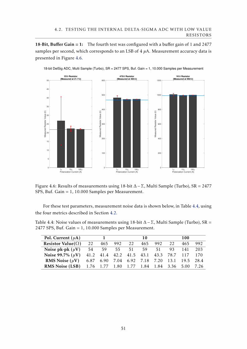
4.2. TESTING THE INTERNAL DELTA-SIGMA ADC WITH LOW VALUE
RESISTORS
18-Bit, Buffer Gain = 1: The fourth test was configured with a buffer gain of 1 and 2477
samples per second, which corresponds to an LSB of 4 µA. Measurement accuracy data is
presented in Figure 4.6.
18-bit DelSig ADC, Multi Sample (Turbo), SR = 2477 SPS, Buf. Gain = 1, 10.000 Samples per Measurement
22 Resistor
(Measured at 21.7 )
1 10 100
Polarization Current (A)
0
5
10
15
20
25
30
35
40
45
50
Me
asu
red
Re
sis
tor
Va
lue
()
470 Resistor
(Measured at 465 )
1 10 100
Polarization Current (A)
0
100
200
300
400
500
600
Me
asu
red
Re
sis
tor
Va
lue
()
1K Resistor
(Measured at 992 )
1 10 100
Polarization Current (A)
0
200
400
600
800
1000
1200
Me
asu
red
Re
sis
tor
Va
lue
()
Figure 4.6: Results of measurements using 18-bit ∆−Σ, Multi Sample (Turbo), SR = 2477SPS, Buf. Gain = 1, 10.000 Samples per Measurement.
For these test parameters, measurement noise data is shown below, in Table 4.4, using
the four metrics described in Section 4.2.
Table 4.4: Noise values of measurements using 18-bit ∆−Σ, Multi Sample (Turbo), SR =2477 SPS, Buf. Gain = 1, 10.000 Samples per Measurement.
Pol. Current (µA) 1 10 100Resistor Value(Ω) 22 465 992 22 465 992 22 465 992Noise pk-pk (µV) 54 59 55 51 59 51 93 141 203Noise 99.7% (µV) 41.2 41.4 42.2 41.5 43.1 43.3 78.7 117 170RMS Noise (µV) 6.87 6.90 7.04 6.92 7.18 7.20 13.1 19.5 28.4
RMS Noise (LSB) 1.76 1.77 1.80 1.77 1.84 1.84 3.36 5.00 7.26
51
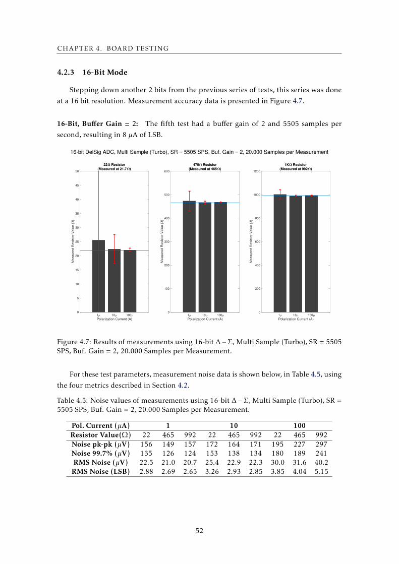
CHAPTER 4. BOARD TESTING
4.2.3 16-Bit Mode
Stepping down another 2 bits from the previous series of tests, this series was done
at a 16 bit resolution. Measurement accuracy data is presented in Figure 4.7.
16-Bit, Buffer Gain = 2: The fifth test had a buffer gain of 2 and 5505 samples per
second, resulting in 8 µA of LSB.
16-bit DelSig ADC, Multi Sample (Turbo), SR = 5505 SPS, Buf. Gain = 2, 20.000 Samples per Measurement
22 Resistor
(Measured at 21.7 )
1 10 100
Polarization Current (A)
0
5
10
15
20
25
30
35
40
45
50
Me
asu
red
Re
sis
tor
Va
lue
()
470 Resistor
(Measured at 465 )
1 10 100
Polarization Current (A)
0
100
200
300
400
500
600
Me
asu
red
Re
sis
tor
Va
lue
()
1K Resistor
(Measured at 992 )
1 10 100
Polarization Current (A)
0
200
400
600
800
1000
1200
Me
asu
red
Re
sis
tor
Va
lue
()
Figure 4.7: Results of measurements using 16-bit ∆−Σ, Multi Sample (Turbo), SR = 5505SPS, Buf. Gain = 2, 20.000 Samples per Measurement.
For these test parameters, measurement noise data is shown below, in Table 4.5, using
the four metrics described in Section 4.2.
Table 4.5: Noise values of measurements using 16-bit ∆−Σ, Multi Sample (Turbo), SR =5505 SPS, Buf. Gain = 2, 20.000 Samples per Measurement.
Pol. Current (µA) 1 10 100Resistor Value(Ω) 22 465 992 22 465 992 22 465 992Noise pk-pk (µV) 156 149 157 172 164 171 195 227 297Noise 99.7% (µV) 135 126 124 153 138 134 180 189 241RMS Noise (µV) 22.5 21.0 20.7 25.4 22.9 22.3 30.0 31.6 40.2
RMS Noise (LSB) 2.88 2.69 2.65 3.26 2.93 2.85 3.85 4.04 5.15
52

4.2. TESTING THE INTERNAL DELTA-SIGMA ADC WITH LOW VALUE
RESISTORS
16-Bit, Buffer Gain = 1: This sixth test returns to unitary buffer gain and uses a sample
rate of 11010 samples per second, with an LSB of 16 µA. Measurement accuracy data is
presented in Figure 4.8.
16-bit DelSig ADC, Multi Sample (Turbo), SR = 11010 SPS, Buf. Gain = 1, 20.000 Samples per Measurement
22 Resistor
(Measured at 21.7 )
1 10 100
Polarization Current (A)
0
5
10
15
20
25
30
35
40
45
50
Me
asu
red
Re
sis
tor
Va
lue
()
470 Resistor
(Measured at 465 )
1 10 100
Polarization Current (A)
0
100
200
300
400
500
600
Me
asu
red
Re
sis
tor
Va
lue
()
1K Resistor
(Measured at 992 )
1 10 100
Polarization Current (A)
0
200
400
600
800
1000
1200
Me
asu
red
Re
sis
tor
Va
lue
()
Figure 4.8: Results of measurements using 16-bit ∆−Σ, Multi Sample (Turbo), SR =11010 SPS, Buf. Gain = 1, 20.000 Samples per Measurement.
For these test parameters, measurement noise data is shown below, in Table 4.6, using
the four metrics described in Section 4.2.
Table 4.6: Noise values of measurements using 16-bit ∆−Σ, Multi Sample (Turbo), SR =11010 SPS, Buf. Gain = 1, 20.000 Samples per Measurement.
Pol. Current (µA) 1 10 100Resistor Value(Ω) 22 465 992 22 465 992 22 465 992Noise pk-pk (µV) 235 281 297 281 312 266 344 375 422Noise 99.7% (µV) 203 228 231 228 251 224 256 278 317RMS Noise (µV) 33.8 37.9 38.5 38.0 41.8 37.3 42.7 46.3 52.8
RMS Noise (LSB) 2.16 2.43 2.47 2.43 2.68 2.38 2.73 2.96 3.38
53
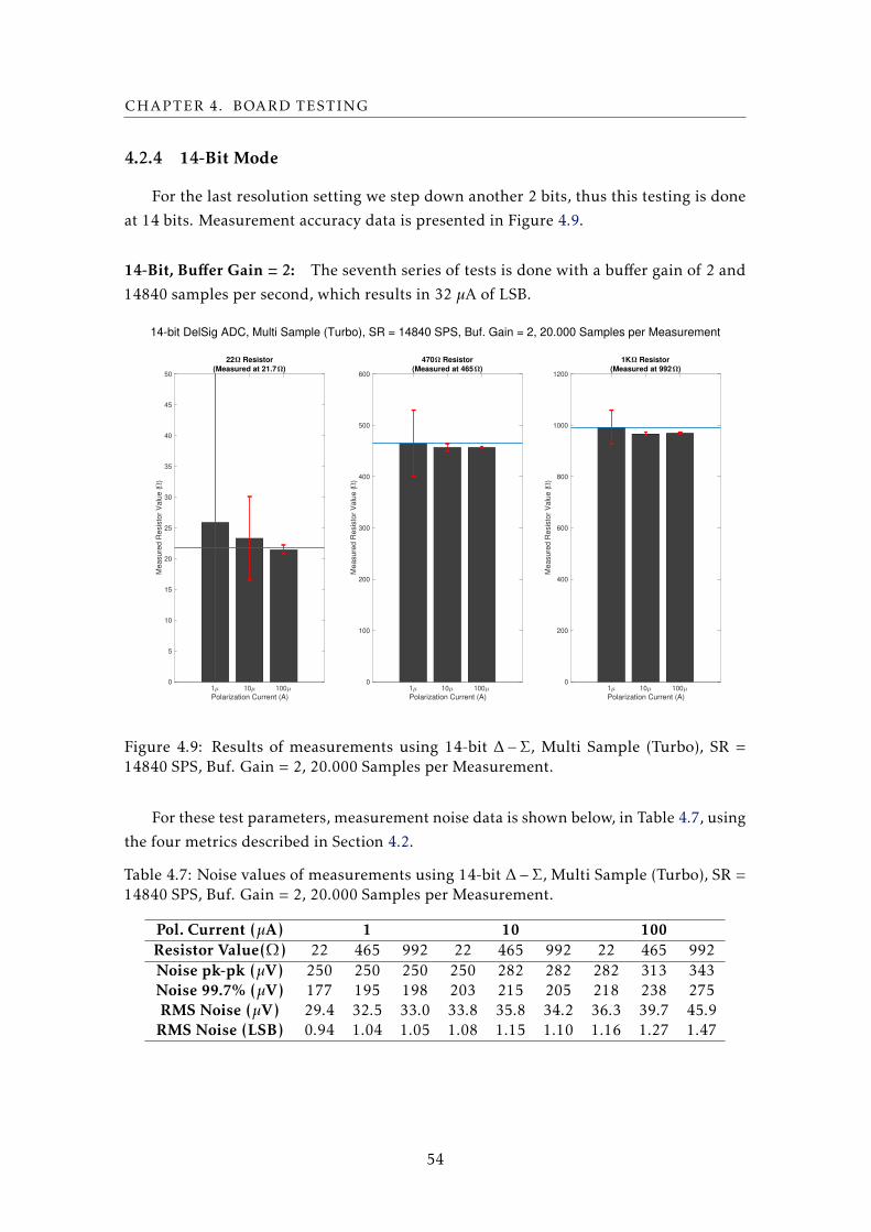
CHAPTER 4. BOARD TESTING
4.2.4 14-Bit Mode
For the last resolution setting we step down another 2 bits, thus this testing is done
at 14 bits. Measurement accuracy data is presented in Figure 4.9.
14-Bit, Buffer Gain = 2: The seventh series of tests is done with a buffer gain of 2 and
14840 samples per second, which results in 32 µA of LSB.
14-bit DelSig ADC, Multi Sample (Turbo), SR = 14840 SPS, Buf. Gain = 2, 20.000 Samples per Measurement
22 Resistor
(Measured at 21.7 )
1 10 100
Polarization Current (A)
0
5
10
15
20
25
30
35
40
45
50
Me
asu
red
Re
sis
tor
Va
lue
()
470 Resistor
(Measured at 465 )
1 10 100
Polarization Current (A)
0
100
200
300
400
500
600
Me
asu
red
Re
sis
tor
Va
lue
()
1K Resistor
(Measured at 992 )
1 10 100
Polarization Current (A)
0
200
400
600
800
1000
1200
Me
asu
red
Re
sis
tor
Va
lue
()
Figure 4.9: Results of measurements using 14-bit ∆−Σ, Multi Sample (Turbo), SR =14840 SPS, Buf. Gain = 2, 20.000 Samples per Measurement.
For these test parameters, measurement noise data is shown below, in Table 4.7, using
the four metrics described in Section 4.2.
Table 4.7: Noise values of measurements using 14-bit ∆−Σ, Multi Sample (Turbo), SR =14840 SPS, Buf. Gain = 2, 20.000 Samples per Measurement.
Pol. Current (µA) 1 10 100Resistor Value(Ω) 22 465 992 22 465 992 22 465 992Noise pk-pk (µV) 250 250 250 250 282 282 282 313 343Noise 99.7% (µV) 177 195 198 203 215 205 218 238 275RMS Noise (µV) 29.4 32.5 33.0 33.8 35.8 34.2 36.3 39.7 45.9
RMS Noise (LSB) 0.94 1.04 1.05 1.08 1.15 1.10 1.16 1.27 1.47
54
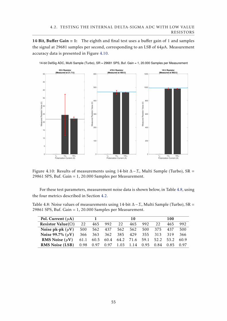
4.2. TESTING THE INTERNAL DELTA-SIGMA ADC WITH LOW VALUE
RESISTORS
14-Bit, Buffer Gain = 1: The eighth and final test uses a buffer gain of 1 and samples
the signal at 29681 samples per second, corresponding to an LSB of 64µA. Measurement
accuracy data is presented in Figure 4.10.
14-bit DelSig ADC, Multi Sample (Turbo), SR = 29681 SPS, Buf. Gain = 1, 20.000 Samples per Measurement
22 Resistor
(Measured at 21.7 )
1 10 100
Polarization Current (A)
0
5
10
15
20
25
30
35
40
45
50
Me
asu
red
Re
sis
tor
Va
lue
()
470 Resistor
(Measured at 465 )
1 10 100
Polarization Current (A)
0
100
200
300
400
500
600
Me
asu
red
Re
sis
tor
Va
lue
()
1K Resistor
(Measured at 992 )
1 10 100
Polarization Current (A)
0
200
400
600
800
1000
1200
Me
asu
red
Re
sis
tor
Va
lue
()
Figure 4.10: Results of measurements using 14-bit ∆−Σ, Multi Sample (Turbo), SR =29861 SPS, Buf. Gain = 1, 20.000 Samples per Measurement.
For these test parameters, measurement noise data is shown below, in Table 4.8, using
the four metrics described in Section 4.2.
Table 4.8: Noise values of measurements using 14-bit ∆−Σ, Multi Sample (Turbo), SR =29861 SPS, Buf. Gain = 1, 20.000 Samples per Measurement.
Pol. Current (µA) 1 10 100Resistor Value(Ω) 22 465 992 22 465 992 22 465 992Noise pk-pk (µV) 500 562 437 562 562 500 375 437 500Noise 99.7% (µV) 366 363 362 385 429 355 313 319 366RMS Noise (µV) 61.1 60.5 60.4 64.2 71.6 59.1 52.2 53.2 60.9
RMS Noise (LSB) 0.98 0.97 0.97 1.03 1.14 0.95 0.84 0.85 0.97
55
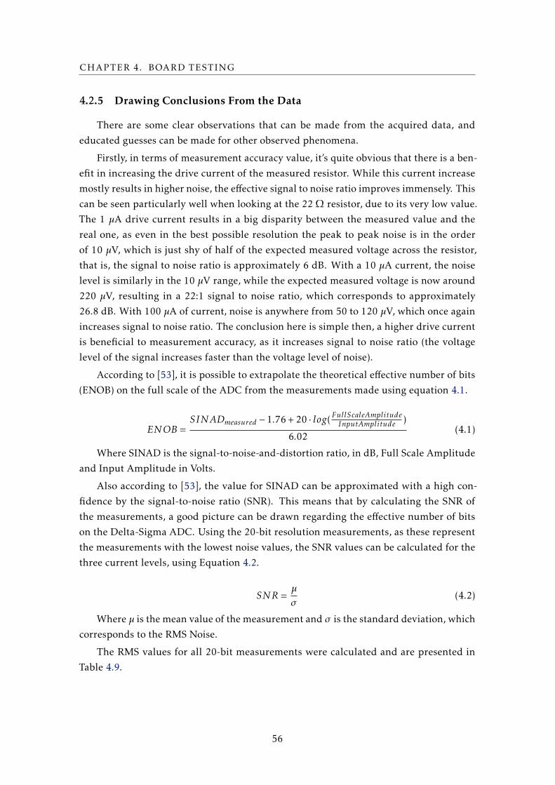
CHAPTER 4. BOARD TESTING
4.2.5 Drawing Conclusions From the Data
There are some clear observations that can be made from the acquired data, and
educated guesses can be made for other observed phenomena.
Firstly, in terms of measurement accuracy value, it’s quite obvious that there is a ben-
efit in increasing the drive current of the measured resistor. While this current increase
mostly results in higher noise, the effective signal to noise ratio improves immensely. This
can be seen particularly well when looking at the 22 Ω resistor, due to its very low value.
The 1 µA drive current results in a big disparity between the measured value and the
real one, as even in the best possible resolution the peak to peak noise is in the order
of 10 µV, which is just shy of half of the expected measured voltage across the resistor,
that is, the signal to noise ratio is approximately 6 dB. With a 10 µA current, the noise
level is similarly in the 10 µV range, while the expected measured voltage is now around
220 µV, resulting in a 22:1 signal to noise ratio, which corresponds to approximately
26.8 dB. With 100 µA of current, noise is anywhere from 50 to 120 µV, which once again
increases signal to noise ratio. The conclusion here is simple then, a higher drive current
is beneficial to measurement accuracy, as it increases signal to noise ratio (the voltage
level of the signal increases faster than the voltage level of noise).
According to [53], it is possible to extrapolate the theoretical effective number of bits
(ENOB) on the full scale of the ADC from the measurements made using equation 4.1.
ENOB =SINADmeasured − 1.76 + 20 · log(FullScaleAmplitudeInputAmplitude )
6.02(4.1)
Where SINAD is the signal-to-noise-and-distortion ratio, in dB, Full Scale Amplitude
and Input Amplitude in Volts.
Also according to [53], the value for SINAD can be approximated with a high con-
fidence by the signal-to-noise ratio (SNR). This means that by calculating the SNR of
the measurements, a good picture can be drawn regarding the effective number of bits
on the Delta-Sigma ADC. Using the 20-bit resolution measurements, as these represent
the measurements with the lowest noise values, the SNR values can be calculated for the
three current levels, using Equation 4.2.
SNR =µ
σ(4.2)
Where µ is the mean value of the measurement and σ is the standard deviation, which
corresponds to the RMS Noise.
The RMS values for all 20-bit measurements were calculated and are presented in
Table 4.9.
56
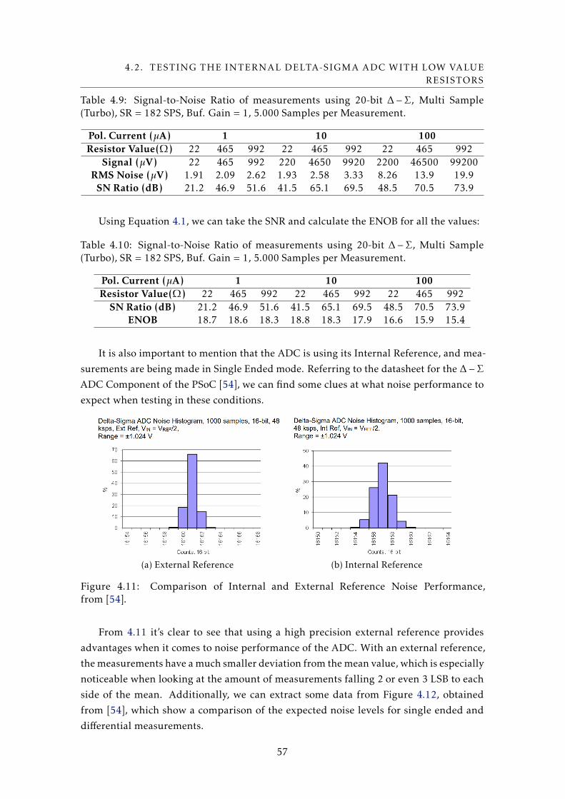
4.2. TESTING THE INTERNAL DELTA-SIGMA ADC WITH LOW VALUE
RESISTORS
Table 4.9: Signal-to-Noise Ratio of measurements using 20-bit ∆−Σ, Multi Sample(Turbo), SR = 182 SPS, Buf. Gain = 1, 5.000 Samples per Measurement.
Pol. Current (µA) 1 10 100Resistor Value(Ω) 22 465 992 22 465 992 22 465 992
Signal (µV) 22 465 992 220 4650 9920 2200 46500 99200RMS Noise (µV) 1.91 2.09 2.62 1.93 2.58 3.33 8.26 13.9 19.9
SN Ratio (dB) 21.2 46.9 51.6 41.5 65.1 69.5 48.5 70.5 73.9
Using Equation 4.1, we can take the SNR and calculate the ENOB for all the values:
Table 4.10: Signal-to-Noise Ratio of measurements using 20-bit ∆−Σ, Multi Sample(Turbo), SR = 182 SPS, Buf. Gain = 1, 5.000 Samples per Measurement.
Pol. Current (µA) 1 10 100Resistor Value(Ω) 22 465 992 22 465 992 22 465 992
SN Ratio (dB) 21.2 46.9 51.6 41.5 65.1 69.5 48.5 70.5 73.9ENOB 18.7 18.6 18.3 18.8 18.3 17.9 16.6 15.9 15.4
It is also important to mention that the ADC is using its Internal Reference, and mea-
surements are being made in Single Ended mode. Referring to the datasheet for the ∆−ΣADC Component of the PSoC [54], we can find some clues at what noise performance to
expect when testing in these conditions.
(a) External Reference (b) Internal Reference
Figure 4.11: Comparison of Internal and External Reference Noise Performance,from [54].
From 4.11 it’s clear to see that using a high precision external reference provides
advantages when it comes to noise performance of the ADC. With an external reference,
the measurements have a much smaller deviation from the mean value, which is especially
noticeable when looking at the amount of measurements falling 2 or even 3 LSB to each
side of the mean. Additionally, we can extract some data from Figure 4.12, obtained
from [54], which show a comparison of the expected noise levels for single ended and
differential measurements.
57
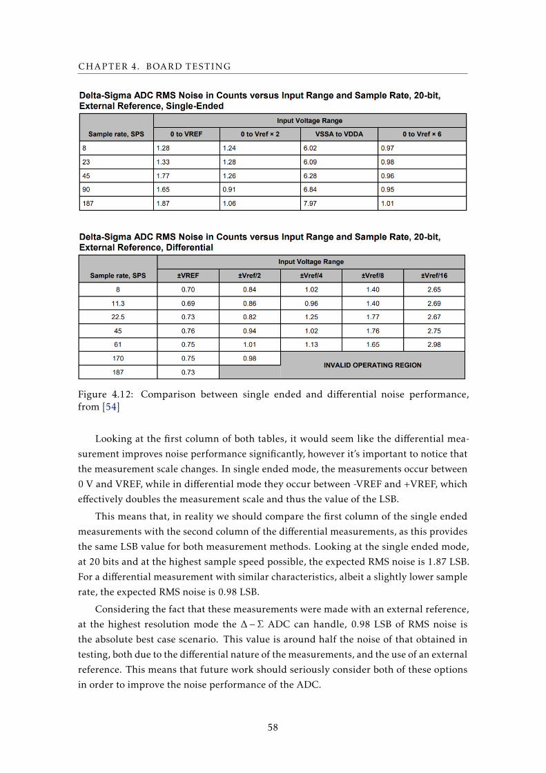
CHAPTER 4. BOARD TESTING
Figure 4.12: Comparison between single ended and differential noise performance,from [54]
Looking at the first column of both tables, it would seem like the differential mea-
surement improves noise performance significantly, however it’s important to notice that
the measurement scale changes. In single ended mode, the measurements occur between
0 V and VREF, while in differential mode they occur between -VREF and +VREF, which
effectively doubles the measurement scale and thus the value of the LSB.
This means that, in reality we should compare the first column of the single ended
measurements with the second column of the differential measurements, as this provides
the same LSB value for both measurement methods. Looking at the single ended mode,
at 20 bits and at the highest sample speed possible, the expected RMS noise is 1.87 LSB.
For a differential measurement with similar characteristics, albeit a slightly lower sample
rate, the expected RMS noise is 0.98 LSB.
Considering the fact that these measurements were made with an external reference,
at the highest resolution mode the ∆−Σ ADC can handle, 0.98 LSB of RMS noise is
the absolute best case scenario. This value is around half the noise of that obtained in
testing, both due to the differential nature of the measurements, and the use of an external
reference. This means that future work should seriously consider both of these options
in order to improve the noise performance of the ADC.
58
4.3. TESTING THE INTERNAL DELTA-SIGMA ADC WITH HIGH VALUE
RESISTORS AND INVESTIGATION INTO THE CURRENT DAC
4.3 Testing the Internal Delta-Sigma ADC with High Value
Resistors and Investigation into the Current DAC
From the testing with low values resistors, one interesting phenomenon can be ob-
served, especially for the measurements with 100 µA of drive current, and that is that
noise increases as the resistor value increases. This is something that should not be
happening, as noise, both in the resistor and the ADC should be relatively constant.
This increase in noise is especially noticeable with higher resolution settings, where the
measurement noise is very low. When using 16 bits of resolution the effect practically
disappears, and when using 14 bits it is completely unnoticeable, most likely due to the
LSB noise overshadowing the strange noise detected.
Because the noise rises with resistor value, and mostly with 100 µA drive current, it is
theorized that this noise is coming from the Current DAC, as the drawn power increases
linearly with resistor value.
To test this hypotheses, 3 tests will be done, with a similar setup to those in Section 4.2,
using 20, 18 and 16 bits of resolution with a unitary buffer gain, and the maximum sample
rate possible for each resolution in Multi Sample (Turbo) mode.
If the noise being measured is coming from the Current DAC, this test should see a
significant increase in noise compared to those in the last Section due to the increase in
current draw being directly proportional to the measured resistor. However, the noise
increase may not be linearly proportional to the drawn current, as there is no way of
knowing what, inside the Current DAC, is the culprit of said noise.
Even if the expected noise increase is measured though, there can still be doubts if
it is coming from the Current DAC or from the ADC itself, so there will be the need to
compare the ADC noise for a high value resistor driven by the Current DAC with another
voltage source that is known to be of very low noise. For this, a simple installation will
be used with a lithium ion battery, which has a voltage of around 4 V, connected to a
resistive divider.
The resistive divider is needed in order to bring the 4 V output from the battery into
the 0 - 1.024 V measurement range of the ADC, however this testing setup will inevitably
introduce some noise due to not only the resistive divider itself, but also the cables and
connections used to interface the battery with the ADC. As such, this test should only be
used to compare the Current DAC with an external voltage source and should not be used
as a de facto baseline for the amount of noise that is to expect from an external sensor.
59
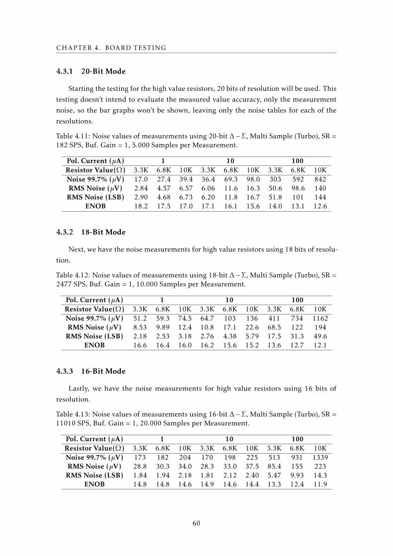
CHAPTER 4. BOARD TESTING
4.3.1 20-Bit Mode
Starting the testing for the high value resistors, 20 bits of resolution will be used. This
testing doesn’t intend to evaluate the measured value accuracy, only the measurement
noise, so the bar graphs won’t be shown, leaving only the noise tables for each of the
resolutions.
Table 4.11: Noise values of measurements using 20-bit ∆−Σ, Multi Sample (Turbo), SR =182 SPS, Buf. Gain = 1, 5.000 Samples per Measurement.
Pol. Current (µA) 1 10 100Resistor Value(Ω) 3.3K 6.8K 10K 3.3K 6.8K 10K 3.3K 6.8K 10KNoise 99.7% (µV) 17.0 27.4 39.4 36.4 69.3 98.0 303 592 842RMS Noise (µV) 2.84 4.57 6.57 6.06 11.6 16.3 50.6 98.6 140
RMS Noise (LSB) 2.90 4.68 6.73 6.20 11.8 16.7 51.8 101 144ENOB 18.2 17.5 17.0 17.1 16.1 15.6 14.0 13.1 12.6
4.3.2 18-Bit Mode
Next, we have the noise measurements for high value resistors using 18 bits of resolu-
tion.
Table 4.12: Noise values of measurements using 18-bit ∆−Σ, Multi Sample (Turbo), SR =2477 SPS, Buf. Gain = 1, 10.000 Samples per Measurement.
Pol. Current (µA) 1 10 100Resistor Value(Ω) 3.3K 6.8K 10K 3.3K 6.8K 10K 3.3K 6.8K 10KNoise 99.7% (µV) 51.2 59.3 74.5 64.7 103 136 411 734 1162RMS Noise (µV) 8.53 9.89 12.4 10.8 17.1 22.6 68.5 122 194
RMS Noise (LSB) 2.18 2.53 3.18 2.76 4.38 5.79 17.5 31.3 49.6ENOB 16.6 16.4 16.0 16.2 15.6 15.2 13.6 12.7 12.1
4.3.3 16-Bit Mode
Lastly, we have the noise measurements for high value resistors using 16 bits of
resolution.
Table 4.13: Noise values of measurements using 16-bit ∆−Σ, Multi Sample (Turbo), SR =11010 SPS, Buf. Gain = 1, 20.000 Samples per Measurement.
Pol. Current (µA) 1 10 100Resistor Value(Ω) 3.3K 6.8K 10K 3.3K 6.8K 10K 3.3K 6.8K 10KNoise 99.7% (µV) 173 182 204 170 198 225 513 931 1339RMS Noise (µV) 28.8 30.3 34.0 28.3 33.0 37.5 85.4 155 223
RMS Noise (LSB) 1.84 1.94 2.18 1.81 2.12 2.40 5.47 9.93 14.3ENOB 14.8 14.8 14.6 14.9 14.6 14.4 13.3 12.4 11.9
60
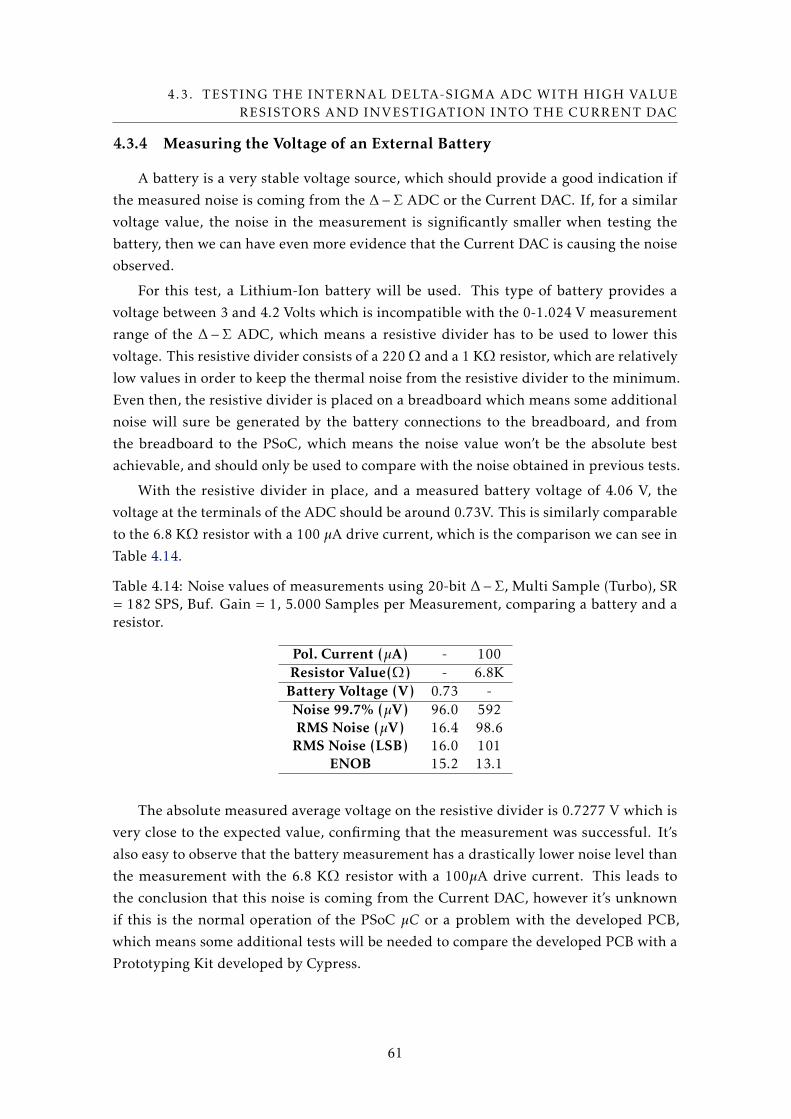
4.3. TESTING THE INTERNAL DELTA-SIGMA ADC WITH HIGH VALUE
RESISTORS AND INVESTIGATION INTO THE CURRENT DAC
4.3.4 Measuring the Voltage of an External Battery
A battery is a very stable voltage source, which should provide a good indication if
the measured noise is coming from the ∆−Σ ADC or the Current DAC. If, for a similar
voltage value, the noise in the measurement is significantly smaller when testing the
battery, then we can have even more evidence that the Current DAC is causing the noise
observed.
For this test, a Lithium-Ion battery will be used. This type of battery provides a
voltage between 3 and 4.2 Volts which is incompatible with the 0-1.024 V measurement
range of the ∆−Σ ADC, which means a resistive divider has to be used to lower this
voltage. This resistive divider consists of a 220 Ω and a 1 KΩ resistor, which are relatively
low values in order to keep the thermal noise from the resistive divider to the minimum.
Even then, the resistive divider is placed on a breadboard which means some additional
noise will sure be generated by the battery connections to the breadboard, and from
the breadboard to the PSoC, which means the noise value won’t be the absolute best
achievable, and should only be used to compare with the noise obtained in previous tests.
With the resistive divider in place, and a measured battery voltage of 4.06 V, the
voltage at the terminals of the ADC should be around 0.73V. This is similarly comparable
to the 6.8 KΩ resistor with a 100 µA drive current, which is the comparison we can see in
Table 4.14.
Table 4.14: Noise values of measurements using 20-bit ∆−Σ, Multi Sample (Turbo), SR= 182 SPS, Buf. Gain = 1, 5.000 Samples per Measurement, comparing a battery and aresistor.
Pol. Current (µA) - 100Resistor Value(Ω) - 6.8K
Battery Voltage (V) 0.73 -Noise 99.7% (µV) 96.0 592RMS Noise (µV) 16.4 98.6
RMS Noise (LSB) 16.0 101ENOB 15.2 13.1
The absolute measured average voltage on the resistive divider is 0.7277 V which is
very close to the expected value, confirming that the measurement was successful. It’s
also easy to observe that the battery measurement has a drastically lower noise level than
the measurement with the 6.8 KΩ resistor with a 100µA drive current. This leads to
the conclusion that this noise is coming from the Current DAC, however it’s unknown
if this is the normal operation of the PSoC µC or a problem with the developed PCB,
which means some additional tests will be needed to compare the developed PCB with a
Prototyping Kit developed by Cypress.
61
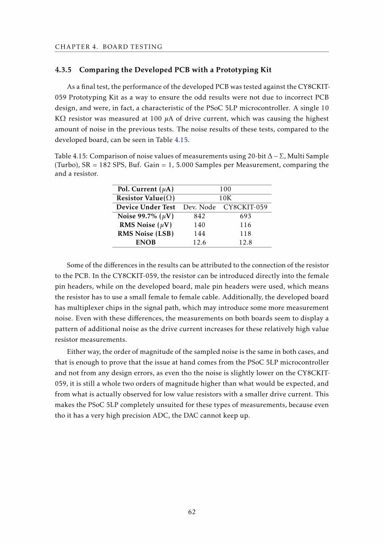
CHAPTER 4. BOARD TESTING
4.3.5 Comparing the Developed PCB with a Prototyping Kit
As a final test, the performance of the developed PCB was tested against the CY8CKIT-
059 Prototyping Kit as a way to ensure the odd results were not due to incorrect PCB
design, and were, in fact, a characteristic of the PSoC 5LP microcontroller. A single 10
KΩ resistor was measured at 100 µA of drive current, which was causing the highest
amount of noise in the previous tests. The noise results of these tests, compared to the
developed board, can be seen in Table 4.15.
Table 4.15: Comparison of noise values of measurements using 20-bit ∆−Σ, Multi Sample(Turbo), SR = 182 SPS, Buf. Gain = 1, 5.000 Samples per Measurement, comparing theand a resistor.
Pol. Current (µA) 100Resistor Value(Ω) 10KDevice Under Test Dev. Node CY8CKIT-059Noise 99.7% (µV) 842 693RMS Noise (µV) 140 116
RMS Noise (LSB) 144 118ENOB 12.6 12.8
Some of the differences in the results can be attributed to the connection of the resistor
to the PCB. In the CY8CKIT-059, the resistor can be introduced directly into the female
pin headers, while on the developed board, male pin headers were used, which means
the resistor has to use a small female to female cable. Additionally, the developed board
has multiplexer chips in the signal path, which may introduce some more measurement
noise. Even with these differences, the measurements on both boards seem to display a
pattern of additional noise as the drive current increases for these relatively high value
resistor measurements.
Either way, the order of magnitude of the sampled noise is the same in both cases, and
that is enough to prove that the issue at hand comes from the PSoC 5LP microcontroller
and not from any design errors, as even tho the noise is slightly lower on the CY8CKIT-
059, it is still a whole two orders of magnitude higher than what would be expected, and
from what is actually observed for low value resistors with a smaller drive current. This
makes the PSoC 5LP completely unsuited for these types of measurements, because even
tho it has a very high precision ADC, the DAC cannot keep up.
62
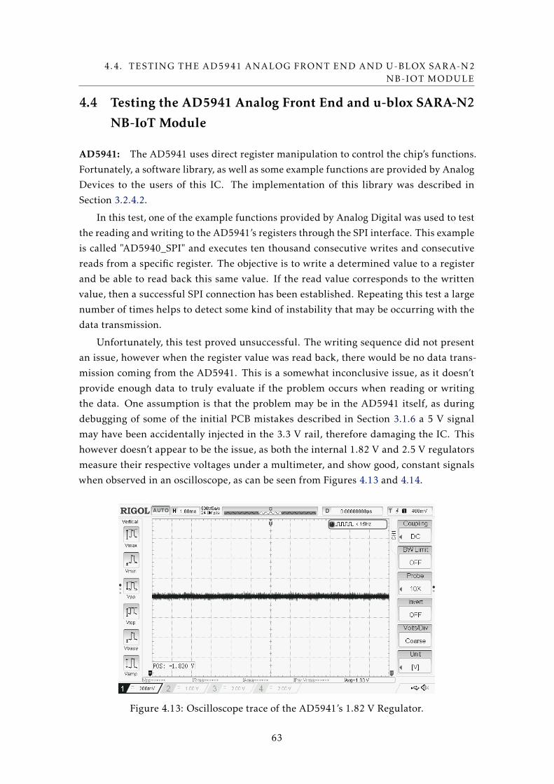
4.4. TESTING THE AD5941 ANALOG FRONT END AND U-BLOX SARA-N2
NB-IOT MODULE
4.4 Testing the AD5941 Analog Front End and u-blox SARA-N2
NB-IoT Module
AD5941: The AD5941 uses direct register manipulation to control the chip’s functions.
Fortunately, a software library, as well as some example functions are provided by Analog
Devices to the users of this IC. The implementation of this library was described in
Section 3.2.4.2.
In this test, one of the example functions provided by Analog Digital was used to test
the reading and writing to the AD5941’s registers through the SPI interface. This example
is called "AD5940_SPI" and executes ten thousand consecutive writes and consecutive
reads from a specific register. The objective is to write a determined value to a register
and be able to read back this same value. If the read value corresponds to the written
value, then a successful SPI connection has been established. Repeating this test a large
number of times helps to detect some kind of instability that may be occurring with the
data transmission.
Unfortunately, this test proved unsuccessful. The writing sequence did not present
an issue, however when the register value was read back, there would be no data trans-
mission coming from the AD5941. This is a somewhat inconclusive issue, as it doesn’t
provide enough data to truly evaluate if the problem occurs when reading or writing
the data. One assumption is that the problem may be in the AD5941 itself, as during
debugging of some of the initial PCB mistakes described in Section 3.1.6 a 5 V signal
may have been accidentally injected in the 3.3 V rail, therefore damaging the IC. This
however doesn’t appear to be the issue, as both the internal 1.82 V and 2.5 V regulators
measure their respective voltages under a multimeter, and show good, constant signals
when observed in an oscilloscope, as can be seen from Figures 4.13 and 4.14.
Figure 4.13: Oscilloscope trace of the AD5941’s 1.82 V Regulator.
63

CHAPTER 4. BOARD TESTING
Figure 4.14: Oscilloscope trace of the AD5941’s 2.5 V Regulator.
These are very unfortunate results, as even several attempts to solve the problem
proved useless. The described issue can also be observed through a Logic Analyzer in
Figures 4.15 and 4.16 .
Figure 4.15: Logic Analyzer Data of a SPI Write Command to the AD5941.
Figure 4.15 shows an SPI Write Command. Initially a byte with 0x20 is sent, this
is defined in the AD5941’s library as "set address", telling the AD5941 that a register
address will follow, which in this case is 0x2230. Another byte is then sent with the
address 0x2D which is a "write address" command, followed by 0xC539151E, randomly
generated data to write into the 0x2230 register.
Similarly to the SPI Write Command, the SPI Read Command shown in Figure 4.16
starts with a 0x20 "set address" command, and the 0x2230 address is sent. Things then
start to differ, as this time a 0x6D "read address" command is sent. After this, a dummy
read is done, then CS is once again pulled low in order to receive data, however the
AD5941 doesn’t respond.
64

4.4. TESTING THE AD5941 ANALOG FRONT END AND U-BLOX SARA-N2
NB-IOT MODULE
The purpose of the dummy read is to generate pulses on the clock line, which the
slave device then detects and replies to. This is the implementation provided in the
AD5941’s library and should be expected to work, but it does not. This means that the
problem is most likely hardware related.
Figure 4.16: Logic Analyzer Data of a SPI Read Command to the AD5941.
u-blox SARA-N2: The u-blox SARA-N2 NB-IoT module was a big bet when designing
this sensor board, however it could not be tested in the allotted time. Testing this module
would require an NB-IoT enabled SIM card and the development of a significant amount
of software which simply there was not enough time for.
65


Chapter
5Conclusion
This dissertation work proposed to create the basis for an adaptable and reconfig-
urable IoT node with the ability to measure data from several environmental sensors with
an extremely high level of accuracy.
An IoT architecture was developed with the use of a state of the art PSoC micro-
controller with a very high resolution ADC and a additional, optional, analog front end
integrated circuit in the form of the Analog Devices AD5941. Multiplexers would tie the
sensor inputs to the ADCs in either the PSoC or the AD5941 in order to accommodate a
larger number of sensors than either of these devices would allow.
Wireless communications would be assured by the u-blox SARA N210 NB-IoT mod-
ule, which allows long distance communication at low data rates, with low energy usage,
over vast distances.
A 4-layer printed circuit board was developed in KiCad containing all the describe
components, while taking into account several layout considerations described in Chap-
ter 3.1. This circuit board was designed in a way that it could form a foundation for future
work in this area, with its design files being made available for change and development.
The developed circuit board was then manufactured by JLCPCB, components were
ordered from Mouser and Digikey and then reflow soldered in a reflow oven. At this point
some unexpected issues arose which delayed development, as the PSoC microcontroller
would not initialize. This issue was tracked to a design mistake in the PCB which was
luckily a relatively easy fix, however it was extremely time consuming, as it took over a
month between diagnosing and ordering new parts.
67
CHAPTER 5. CONCLUSION
With the PCB issue remedied, software was developed to test the different compo-
nents of the board, starting with the simplest which were the MAX14661 multiplexers,
then following with the PSoC microcontroller and the AD5941 analog front end module.
All six of the MAX14661 multiplexers were tested and worked with no issues. Moving
on to the PSoC microcontroller, tests were made at various ADC resolutions and sample
rates, with some unexpected results, both positively and negatively. To start, the 20-bit
Delta-Sigma ADC has extremely good noise performance, generating some very impres-
sive results when testing resistors at low drive currents such as 1 and 10 µA, resulting in
an effective number of bits (ENOB) which is calculated to be above 18 bits and almost as
high as 19 bits for the best case scenario, while also having 15.2 effective bits measured
in the battery comparison made in Chapter 4.14, which is a non-ideal scenario as there is
a resistive divider and some questionable quality connectors involved.
There were however some negative results at higher currents, and with higher resistor
values, which were investigated and tracked to be caused by an extremely noisy output
coming from the current DACs. This was extremely unfortunate as it means that the high
resolution ADC is almost completely useless in these tests, resulting in an ENOB as low
as only 12.6 when measuring at a 20-bit resolution, meaning that the only thing the ADC
effectively measures is noise being generated by the DAC. These tests are presented in
length in Chapters 4.2 and 4.3.
When it came to AD5941 analog front end module, it was discovered that it was
unresponsive to user commands, either through severe user error, which seems unlikely
as the library which implements the AD5941 functionality is very simple to import for
a given microcontroller architecture, or due to hardware issues which possibly occurred
when diagnosing the initial problems with the PSoC microcontroller. Either way, testing
of the AD5941 was impossible to realize, which is extremely unfortunate, as this module
appears to be very promising, as it contains an extremely good suite of ADCs and DACs
specially designed to interface with sensors which need very high precision measurements
such as skin and body impedance or electrochemical toxic gas sensing.
5.1 Future Work
There is a relatively high likelihood of future work being developed on top of the
developed IoT node, therefore the project was uploaded to GitHub at GitHub - KNoT.
This also means that some tips or recommendations will be rather important.
Firstly, it is very important to understand the capabilities of the AD5941, as this
module appears to be extremely capable in the application this IoT node is designed to
fulfill. Not being able to even run basic tests on this chip is probably one of the biggest
disappointments of this dissertation.
Evaluation boards for this module are available, although they are prohibitively ex-
pensive, however a simple test setup can be developed by designing a small, custom
68
5.1. FUTURE WORK
made "evaluation board"which provides an SPI connection to an external off the shelf
microcontroller board such as Arduino or a Raspberry Pi for data communication, and
exposes the sensor input ports of the AD5941 to a small sensor connector. This will not
only help validate the performance claims of this module, but also develop the required
interface software.
If this module does as much as it advertises, it is important to chose a clear direction
about whether to integrate it directly into the mainboard, as this can lead to a different
strategy regarding the main microcontroller platform, as the choice of PSoC 5LP hinged
mainly on its signal acquisition capabilities which were tested and found not to be very
satisfactory, meaning that it could then be switched to a more powerful and cheaper one,
such as the STM32 family, leading to an improvement in the node’s signal capabilities
which can help with filtering and processing measured data.
Regarding the NB-IoT module, a lot of work also needs to be put into it regarding
software interfacing and general RF testing, specially as NB-IoT is still a somewhat niche
communication standard with limited software support. Between the AD5941 and the
NB-IoT node, there is easily enough research work for two dissertations, specially as they
both require a lot of testing and data gathering, as they are relatively new and unexplored
platforms.
Some additional considerations were also discussed in Chapter 3.1.6 regarding devel-
opments to the current printed circuit board, namely the placement of additional pins
connecting the AD5941’s GPIOs and RESET pins to the mainboard.
To summarize, as future work, it is important to:
• Research and test the capabilities of the AD5941.
• Research and test the SARA-N2 NB-IoT module.
• Decide whether to integrate the AD5941 in the mainboard.
• Decide between continuing to use the PSoC microcontroller or switch to an alterna-
tive platform.
69

Bibliography
[1] Z. Xinhua and L. Hong. “A Self-Reconfigurable Sensor Network Constructon
Reaseach in the Paradigm of Internet of Things.” In: 2012 International Confer-ence on Computer Science and Service System. Aug. 2012, pp. 311–314. doi: 10.
1109/CSSS.2012.85.
[2] D. Singh, G. Tripathi, and A. J. Jara. “A survey of Internet-of-Things: Future vision,
architecture, challenges and services.” In: 2014 IEEE World Forum on Internet ofThings (WF-IoT). Mar. 2014, pp. 287–292. doi: 10.1109/WF-IoT.2014.6803174.
[3] I. T. Union. Recommendation ITU-T Y.2060. Overview of the Internet of things. June
2012. url: http://handle.itu.int/11.1002/1000/11559-en?locatt=format:
pdf&auth.
[4] A. Glória, F. Cercas, and N. Souto. “Comparison of communication protocols for
low cost Internet of Things devices.” In: 2017 South Eastern European Design Au-tomation, Computer Engineering, Computer Networks and Social Media Conference(SEEDA-CECNSM). Sept. 2017, pp. 1–6. doi: 10.23919/SEEDA-CECNSM.2017.
8088226.
[5] Cypress. Cypress PSoC® 6 Microcontrollers. Purpose-Built for the Internet of Things.url: https://www.cypress.com/file/386296/download.
[6] M. Electronics. Internet of Things. IoT Sensor Node Block Diagram. url: https:
//eu.mouser.com/applications/internet-of-things-block-diagram/.
[7] A. A. Abudaqa, T. M. Al-Kharoubi, M. F. Mudawar, and A. Kobilica. “Simulation
of ARM and x86 microprocessors using in-order and out-of-order CPU models
with Gem5 simulator.” In: 2018 5th International Conference on Electrical and Elec-tronic Engineering (ICEEE). May 2018, pp. 317–322. doi: 10.1109/ICEEE2.2018.
8391354.
[8] Z. Ou, B. Pang, Y. Deng, J. K. Nurminen, A. Ylä-Jääski, and P. Hui. “Energy- and
Cost-Efficiency Analysis of ARM-Based Clusters.” In: 2012 12th IEEE/ACM Inter-national Symposium on Cluster, Cloud and Grid Computing (ccgrid 2012). May 2012,
pp. 115–123. doi: 10.1109/CCGrid.2012.84.
[9] P. Greenhalgh. Big.LITTLE Processing with ARM Cortex™-A15 & Cortex-A7. Im-proving Energy Efficiency in High-Performance Mobile Platforms. Sept. 2011. url:
https://www.cl.cam.ac.uk/~rdm34/big.LITTLE.pdf.
71
BIBLIOGRAPHY
[10] Z. Wang, Y. Liu, Y. Sun, Y. Li, D. Zhang, and H. Yang. “An energy-efficient het-
erogeneous dual-core processor for Internet of Things.” In: 2015 IEEE Interna-tional Symposium on Circuits and Systems (ISCAS). May 2015, pp. 2301–2304. doi:
10.1109/ISCAS.2015.7169143.
[11] J. Yiu. ARM® Cortex®-M for Beginners. An overview of the ARM Cortex-M processorfamily and comparison. Sept. 2012. url: https://community.arm.com/cfs-
file/__key/telligent-evolution-components-attachments/01-2142-00-00-
00-00-52-96/White-Paper-_2D00_-Cortex_2D00_M-for-Beginners-_2D00_-
2016-_2800_final-v3_2900_.pdf.
[12] C. C. Corporation, H.-P. Company, I. Corporation, L. T. Inc, M. Corporation, N.
Corporation, and K. P. E. N.V. Universal Serial Bus Specification. Apr. 2000. url:
https://www.usb.org/document-library/usb-20-specification.
[13] M. Lauridsen, R. Krigslund, M. Rohr, and G. Madueno. “An Empirical NB-IoT
Power Consumption Model for Battery Lifetime Estimation.” In: 2018 IEEE 87thVehicular Technology Conference (VTC Spring). June 2018, pp. 1–5. doi: 10.1109/
VTCSpring.2018.8417653.
[14] Y. E. Wang, X. Lin, A. Adhikary, A. Grovlen, Y. Sui, Y. Blankenship, J. Bergman,
and H. S. Razaghi. “A Primer on 3GPP Narrowband Internet of Things.” In: IEEECommunications Magazine 55.3 (Mar. 2017), pp. 117–123. issn: 1558-1896. doi:
10.1109/MCOM.2017.1600510CM.
[15] F. Adelantado, X. Vilajosana, P. Tuset-Peiro, B. Martinez, J. Melia-Segui, and T.
Watteyne. “Understanding the Limits of LoRaWAN.” In: IEEE CommunicationsMagazine 55.9 (Sept. 2017), pp. 34–40. issn: 1558-1896. doi: 10.1109/MCOM.
2017.1600613.
[16] B. Rajesh, A. Agarwal, and K. A. Saravanan. “Proficient modus operandi for scru-
tinize air pollution using wireless sensor network.” In: 2014 International Confer-ence on Circuits, Power and Computing Technologies [ICCPCT-2014]. Mar. 2014,
pp. 1312–1316. doi: 10.1109/ICCPCT.2014.7054852.
[17] T. Liu, Z. Liu, and R. W. Jones. “The Evolution of Air Pollution Monitoring and
Modelling in Zhejiang Province.” In: 2019 14th IEEE Conference on Industrial Elec-tronics and Applications (ICIEA). June 2019, pp. 107–112. doi: 10.1109/ICIEA.
2019.8834054.
[18] M. Mukta, S. Islam, S. D. Barman, A. W. Reza, and M. S. Hossain Khan. “Iot
based Smart Water Quality Monitoring System.” In: 2019 IEEE 4th InternationalConference on Computer and Communication Systems (ICCCS). Feb. 2019, pp. 669–
673. doi: 10.1109/CCOMS.2019.8821742.
72

BIBLIOGRAPHY
[19] L. Mezzera, M. Carminati, M. Di Mauro, A. Turolla, M. Tizzoni, and M. Antonelli.
“A 7-Parameter Platform for Smart and Wireless Networks Monitoring On-Line Wa-
ter Quality.” In: 2018 25th IEEE International Conference on Electronics, Circuits andSystems (ICECS). Dec. 2018, pp. 709–712. doi: 10.1109/ICECS.2018.8618014.
[20] B. Das and P. C. Jain. “Real-time water quality monitoring system using Internet
of Things.” In: 2017 International Conference on Computer, Communications andElectronics (Comptelix). July 2017, pp. 78–82. doi: 10.1109/COMPTELIX.2017.
8003942.
[21] N. Vijayakumar and R. Ramya. “The real time monitoring of water quality in
IoT environment.” In: 2015 International Conference on Innovations in Information,Embedded and Communication Systems (ICIIECS). Mar. 2015, pp. 1–5. doi: 10.
1109/ICIIECS.2015.7193080.
[22] P. Sharma and D. V. Padole. “Design and implementation soil analyser using IoT.”
In: 2017 International Conference on Innovations in Information, Embedded and Com-munication Systems (ICIIECS). Mar. 2017, pp. 1–5. doi: 10.1109/ICIIECS.2017.
8275947.
[23] P. Rajalakshmi and S. Devi Mahalakshmi. “IOT based crop-field monitoring and
irrigation automation.” In: 2016 10th International Conference on Intelligent Systemsand Control (ISCO). Jan. 2016, pp. 1–6. doi: 10.1109/ISCO.2016.7726900.
[24] O. Pandithurai, S. Aishwarya, B. Aparna, and K. Kavitha. “Agro-tech: A digi-
tal model for monitoring soil and crops using internet of things (IOT).” In: 2017Third International Conference on Science Technology Engineering Management (ICON-STEM). Mar. 2017, pp. 342–346. doi: 10.1109/ICONSTEM.2017.8261306.
[25] R. D. Down. “Temperature Measurement.” In: Environmental Instrumentation andAnalysis Handbook. John Wiley & Sons, Ltd, 2005. Chap. 21, pp. 445–458. isbn:
9780471473336. doi: 10.1002/0471473332.ch21. url: https://onlinelibrary.
wiley.com/doi/abs/10.1002/0471473332.ch21.
[26] J. R. Gray. “Conductivity Analyzers and Their Application.” In: Environmental In-strumentation and Analysis Handbook. John Wiley & Sons, Ltd, 2005. Chap. 23,
pp. 491–510. isbn: 9780471473336. doi: 10 . 1002 / 0471473332 . ch23. url:
https://onlinelibrary.wiley.com/doi/abs/10.1002/0471473332.ch23.
[27] P. M. Ramos, J. M. D. Pereira, H. M. G. Ramos, and A. L. Ribeiro. “A Four-Terminal
Water-Quality-Monitoring Conductivity Sensor.” In: IEEE Transactions on Instru-mentation and Measurement 57.3 (Mar. 2008), pp. 577–583. issn: 1557-9662. doi:
10.1109/TIM.2007.911703.
[28] A. D. Inc. ADI Water Analysis Solution for pH Meters and Conductivity Meters. 2013.
url: https://www.analog.com/media/cn/technical-documentation/apm-
pdf/adi-water-analysis-solutions_en.pdf.
73
BIBLIOGRAPHY
[29] E. A. Atekwana, E. A. Atekwana, R. S. Rowe, D. D. Werkema, and F. D. Legall. “The
relationship of total dissolved solids measurements to bulk electrical conductivity
in an aquifer contaminated with hydrocarbon.” In: Journal of Applied Geophysics56.4 (2004), pp. 281 –294. issn: 0926-9851. doi: https://doi.org/10.1016/
j.jappgeo.2004.08.003. url: http://www.sciencedirect.com/science/
article/pii/S0926985104000576.
[30] J. R. Gray. “pH Analyzers and Their Application.” In: Environmental Instrumen-tation and Analysis Handbook. John Wiley & Sons, Ltd, 2005. Chap. 22, pp. 459–
490. isbn: 9780471473336. doi: 10.1002/0471473332.ch22. url: https://
onlinelibrary.wiley.com/doi/abs/10.1002/0471473332.ch22.
[31] T. I. Incorporated. SAR ADCs vs. Delta-Sigma ADCs: Different architectures fordifferent application needs. 2015. url: https://training.ti.com/adcwebinar.
[32] G. Castro. Rarely Asked Questions—Issue 133 Common Sense for Current Sensing.
2013. url: https://www.analog.com/media/en/analog-dialogue/raqs/raq-
issue-133.pdf.
[33] N. Paulino. Analog to Digital Converters. Electrónica III Course Presentation at DEE
- FCT/UNL. 2016-2017.
[34] P. Horowitz and W. Hill. The Art of Electronics. 3rd. USA: Cambridge University
Press, 2015. isbn: 0521809266.
[35] U. Farooq, Z. Marrakchi, and H. Mehrez. Tree-based Heterogeneous FPGA Archi-tectures: Application Specific Exploration and Optimization. SpringerLink : Bücher.
Springer New York, 2012. isbn: 9781461435945. url: https://books.google.
pt/books?id=FGGeSu\_txOAC.
[36] S. Dhote, P. Charjan, A. Phansekar, A. Hegde, S. Joshi, and J. Joshi. “Using FPGA-
SoC interface for low cost IoT based image processing.” In: 2016 InternationalConference on Advances in Computing, Communications and Informatics (ICACCI).Sept. 2016, pp. 1963–1968. doi: 10.1109/ICACCI.2016.7732339.
[37] X. Zhang, X. Liu, A. Ramachandran, C. Zhuge, S. Tang, P. Ouyang, Z. Cheng,
K. Rupnow, and D. Chen. “High-performance video content recognition with
long-term recurrent convolutional network for FPGA.” In: 2017 27th InternationalConference on Field Programmable Logic and Applications (FPL). Sept. 2017, pp. 1–4.
doi: 10.23919/FPL.2017.8056833.
[38] F. Baskaya, S. Reddy, Sung Kyu Lim, and D. V. Anderson. “Placement for large-scale
floating-gate field-programable analog arrays.” In: IEEE Transactions on Very LargeScale Integration (VLSI) Systems 14.8 (Aug. 2006), pp. 906–910. issn: 1557-9999.
doi: 10.1109/TVLSI.2006.878477.
74
BIBLIOGRAPHY
[39] C. M. Twigg and P. Hasler. “A Large-Scale Reconfigurable Analog Signal Processor
(RASP) IC.” In: IEEE Custom Integrated Circuits Conference 2006. Sept. 2006, pp. 5–
8. doi: 10.1109/CICC.2006.320937.
[40] A. Basu, S. Brink, C. Schlottmann, S. Ramakrishnan, C. Petre, S. Koziol, F. Baskaya,
C. M. Twigg, and P. Hasler. “A Floating-Gate-Based Field-Programmable Analog
Array.” In: IEEE Journal of Solid-State Circuits 45.9 (Sept. 2010), pp. 1781–1794.
issn: 1558-173X. doi: 10.1109/JSSC.2010.2056832.
[41] S. Brink, J. Hasler, and R. Wunderlich. “Adaptive Floating-Gate Circuit Enabled
Large-Scale FPAA.” In: IEEE Transactions on Very Large Scale Integration (VLSI)Systems 22.11 (Nov. 2014), pp. 2307–2315. issn: 1557-9999. doi: 10.1109/TVLSI.
2013.2290305.
[42] C. R. Schlottmann, S. Shapero, S. Nease, and P. Hasler. “A Digitally Enhanced
Dynamically Reconfigurable Analog Platform for Low-Power Signal Processing.”
In: IEEE Journal of Solid-State Circuits 47.9 (Sept. 2012), pp. 2174–2184. issn:
1558-173X. doi: 10.1109/JSSC.2012.2194847.
[43] A. Malcher and P. Falkowski. “Analog Reconfigurable Circuits.” In: InternationalJournal of Electronics and Telecommunications 60 (Mar. 2014). doi: 10.2478/eletel-
2014-0002.
[44] J. Mocnej, M. Miškuf, P. Papcun, and I. Zolotová. “Impact of Edge Computing
Paradigm on Energy Consumption in IoT.” In: IFAC-PapersOnLine 51.6 (2018).
15th IFAC Conference on Programmable Devices and Embedded Systems PDeS
2018, pp. 162 –167. issn: 2405-8963. doi: https://doi.org/10.1016/j.ifacol.
2018.07.147. url: http://www.sciencedirect.com/science/article/pii/
S2405896318308917.
[45] M. A. López Peña and I. Muñoz Fernández. “SAT-IoT: An Architectural Model
for a High-Performance Fog/Edge/Cloud IoT Platform.” In: 2019 IEEE 5th WorldForum on Internet of Things (WF-IoT). Apr. 2019, pp. 633–638. doi: 10.1109/WF-
IoT.2019.8767282.
[46] ADuCM355 Data Sheet. Rev. C. Analog Devices. Apr. 2020. url: https://www.
analog.com/media/en/technical- documentation/data- sheets/ADuCM355.
pdf.
[47] AD5940/AD5941 Data Sheet. Rev. B. Analog Devices. Mar. 2020. url: https://
www.analog.com/media/en/technical-documentation/data-sheets/AD5940-
5941.pdf.
[48] MAX14661 Data Sheet. Revision 2. Maxim Integrated. Jan. 2015. url: https:
//datasheets.maximintegrated.com/en/ds/MAX14661.pdf.
[49] J. Charras and KiCad Developers Team. KiCad. Version 5.1.7. Nov. 28, 2020. url:
https://kicad.org/.
75
BIBLIOGRAPHY
[50] “Fundamentals of Grounding Design.” In: Grounds for Grounding. John Wiley &
Sons, Ltd, 2010. Chap. 4, pp. 155–322. isbn: 9780470529324. doi: 10.1002/
9780470529324.ch4.
[51] SARA-N2 series Data Sheet. R18. u-blox. Nov. 2019. url: https://www.u-
blox.com/en/docs/UBX-15025564.
[52] AN77900 - PSoC 3 and PSoC 5LP Low-Power Modes and Power Reduction Techniques.Version G. Cypress Semiconductor. May 2020. url: https://www.cypress.com/
documentation/application- notes/an77900- psoc-3-and-psoc-5lp-low-
power-modes-and-power-reduction.
[53] W. Kester. Understand SINAD, ENOB, SNR, THD, THD + N, and SFDR so You Don’tGet Lost in the Noise Floor. Rev. A. Analog Devices. Oct. 2008. url: https:
//www.analog.com/media/en/training-seminars/tutorials/MT-003.pdf.
[54] Delta Sigma Analog to Digital Converter. Version 3.30. Cypress Semiconductor. Sept.
2020. url: https://www.cypress.com/file/400466/download.
76

Appendix
ACode For the Initial MUX and ADC
Experiments
1 #include <p r o j e c t . h>
2 #include " s t d i o . h"
3
4 /* UART Defines */5 # def ine FALSE 0
6 # def ine TRUE 1
7 # def ine TRANSMIT_BUFFER_SIZE 16
8
9 /* There are 8 input channels */10 # def ine NUMCHAN (8u )
11
12 i n t main ( )
13
14 /* I n i t i a l i z e v a r i a b l e that i n d i c a t e s which mux channel
15 i s displayed on LCD */16 uint8 curChan = 0u , transChan ;
17 AMux_1_Init ( ) ;
18 AMux_1_FastSelect ( curChan ) ;
19 /* Variable to s t o r e ADC r e s u l t */20 uint32 Output0 = 0 ;
21 uint32 Output1 = 0 ;
22 /* Variable to s t o r e UART rece ived c h a r a c t e r */23 uint8 Ch ;
24 /* Flags used to s t o r e transmit data commands */25 uint8 ContinuouslySendData ;
26 uint8 SendSingleByte ;
27 /* Transmit Buffer */28 char TransmitBuffer [TRANSMIT_BUFFER_SIZE ] ;
29
77
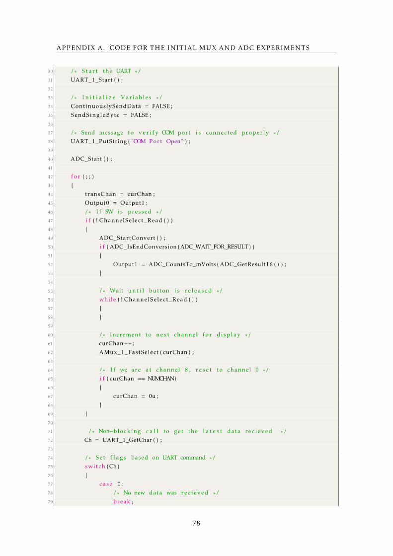
APPENDIX A. CODE FOR THE INITIAL MUX AND ADC EXPERIMENTS
30 /* S t a r t the UART */31 UART_1_Start ( ) ;
32
33 /* I n i t i a l i z e Var iables */34 ContinuouslySendData = FALSE ;
35 SendSingleByte = FALSE ;
36
37 /* Send message to v e r i f y COM port i s connected properly */38 UART_1_PutString ( "COM Port Open" ) ;
39
40 ADC_Start ( ) ;
41
42 fo r ( ; ; )
43
44 transChan = curChan ;
45 Output0 = Output1 ;
46 /* I f SW i s pressed */47 i f ( ! ChannelSelect_Read ( ) )
48
49 ADC_StartConvert ( ) ;
50 i f ( ADC_IsEndConversion (ADC_WAIT_FOR_RESULT) )
51
52 Output1 = ADC_CountsTo_mVolts ( ADC_GetResult16 ( ) ) ;
53
54
55 /* Wait u n t i l button i s r e l e a s e d */56 while ( ! ChannelSelect_Read ( ) )
57
58
59
60 /* Increment to next channel fo r display */61 curChan++;
62 AMux_1_FastSelect ( curChan ) ;
63
64 /* I f we are at channel 8 , r e s e t to channel 0 */65 i f ( curChan == NUMCHAN)
66
67 curChan = 0u ;
68
69
70
71 /* Non−blocking c a l l to get the l a t e s t data rec ieved */72 Ch = UART_1_GetChar ( ) ;
73
74 /* Set f l a g s based on UART command */75 switch (Ch)
76
77 case 0 :
78 /* No new data was rec ieved */79 break ;
78
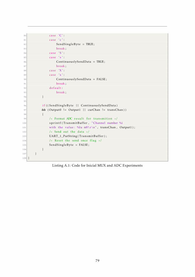
80 case ’C ’ :
81 case ’ c ’ :
82 SendSingleByte = TRUE;
83 break ;
84 case ’ S ’ :
85 case ’ s ’ :
86 ContinuouslySendData = TRUE;
87 break ;
88 case ’X ’ :
89 case ’ x ’ :
90 ContinuouslySendData = FALSE ;
91 break ;
92 defaul t :
93 break ;
94
95
96 i f ( ( SendSingleByte | | ContinuouslySendData )
97 && ( Output0 != Output1 | | curChan != transChan ) )
98
99 /* Format ADC r e s u l t f or transmit ion */100 s p r i n t f ( TransmitBuffer , " Channel number %i
101 with the value : %lu mV\ r \n" , transChan , Output1 ) ;
102 /* Send out the data */103 UART_1_PutString ( TransmitBuffer ) ;
104 /* Reset the send once f l a g */105 SendSingleByte = FALSE ;
106
107
108
Listing A.1: Code for Inicial MUX and ADC Experiments
79

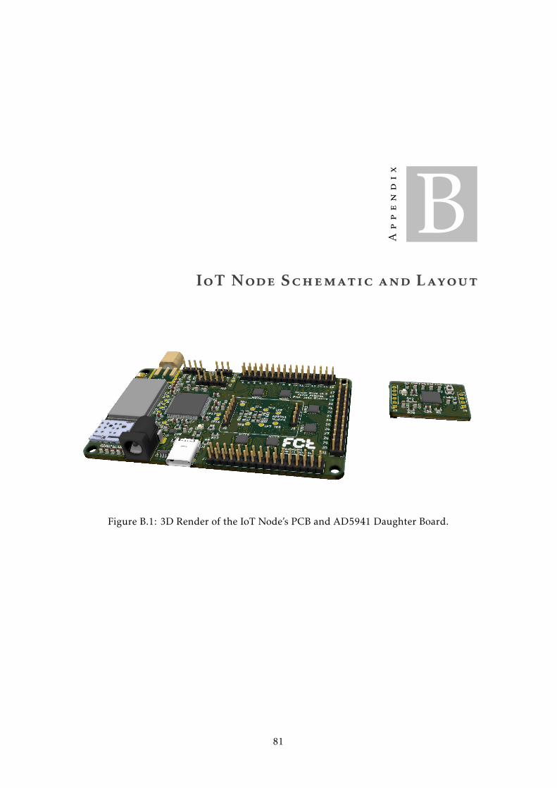
Appendix
BIoT Node Schematic and Layout
Figure B.1: 3D Render of the IoT Node’s PCB and AD5941 Daughter Board.
81
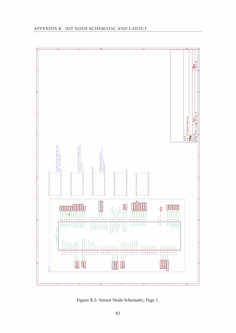
APPENDIX B. IOT NODE SCHEMATIC AND LAYOUT
12
34
56
12
34
56
A B C D
A B C D
Dat
e:
KiC
ad E
.D.A
. ki
cad
(5.1
.5)-
3R
ev:
Siz
e: A
4Id
: 1/6
Tit
le:
File
: IoT
Sen
sor
Nod
e.sc
hS
heet
: /
She
et: I
oT S
enso
r N
ode
HP
FE
File
: IoT
Sen
sor
Nod
e H
PF
E.s
ch
She
et: I
oT S
enso
r N
ode
RF
File
: IoT
Sen
sor
Nod
e R
F.s
ch
She
et: I
oT S
enso
r N
ode
Con
nect
ors
File
: IoT
Sen
sor
Nod
e C
onne
ctor
s.sc
h
She
et: I
oT S
enso
r N
ode
Mux
File
: IoT
Sen
sor
Nod
e M
ux.s
ch
She
et: I
oT S
enso
r N
ode
Pow
er
File
: IoT
Sen
sor
Nod
e P
ower
.sch
TP
17T
estP
oint
TP
16T
estP
oint
P2_
51
VS
SB
10
VD
DIO
210
0
IND
11
VB
OO
ST
12
VB
AT
13
VS
SD
@1
14
XR
ES
15P
5_0
16
P5_
117
P5_
218
P5_
319
P2_
62
P1_
0,S
WD
IO,T
MS
20
P1_
1,S
WD
CK
,TC
K21
P1_
222
P1_
3,S
WV
,TD
O23
P1_
4,T
DI
24
P1_
5,N
TR
ST
25
VD
DIO
126
P1_
627
P1_
728
SIO
,P12
_629
P2_
73
SIO
,P12
_730
P5_
431
P5_
532
P5_
633
P5_
734
US
BD
+,P
15_6
35
US
BD
-,P
15_7
36
VD
DD
@1
37
VS
SD
@2
38
VC
CD
@1
39
SIO
,P12
_44
MH
ZX
OU
T,P
15_0
42
MH
ZX
IN,P
15_1
43
P3_
0,ID
AC
144
P3_
1,ID
AC
345
P3_
2,O
A3-
46
P3_
3,O
A3+
47
P3_
4,O
A1-
48
P3_
5,O
A1-
49
SIO
,P12
_55
VD
DIO
350
P3_
6,O
A1O
UT
51
P3_
7,O
A3O
UT
52
SIO
,P12
_053
SIO
,P12
_154
KH
ZX
OU
T,P
15_2
55
KH
ZX
IN,P
15_3
56
P6_
46
VC
CA
63
VS
SA
64
VD
DA
65
VS
SD
@3
66
SIO
,P12
_267
SIO
,P12
_368
P4_
069
P6_
57
P4_
170
P0_
0,O
A2O
UT
71
P0_
1,O
A1O
UT
72
P0_
2,O
A0+
73
P0_
3,O
A0-
74
VD
DIO
075
P0_
4,O
A2+
76
P0_
5,O
A2-
77
P0_
6,ID
AC
078
P0_
7,ID
AC
279
P6_
68
P4_
280
P4_
381
P4_
482
P4_
583
P4_
684
P4_
785
VC
CD
@2
86
VS
SD
@4
87
VD
DD
@2
88
P6_
089
P6_
79
P6_
190
P6_
291
P6_
392
P15
_493
P15
_594
P2_
095
P2_
196
P2_
297
P2_
398
P2_
499
U1
CY
8C58
88A
XI-
LP09
6
VC
C1
VC
C2
VC
CA
VD
DA
MU
X3_
CS
AD
5941
_CS
MU
X1_
CS
MU
X2_
CS
MU
X6_
CS
MU
X5_
CS
VD
D2
MU
X4_
CS
VS
SA
VD
D1
SP
I_S
CLK
SP
I_M
OS
IS
PI_
MIS
O
SW
DIO
SW
DC
LK
RS
TS
AR
A_T
XD
SA
RA
_RX
DS
AR
A_R
ES
ET
SA
RA
_CT
S
MU
X1_
AV
DD
IO0
VD
DIO
1
I2C
_3V
3_S
DA
I2C
_3V
3_S
CL
VD
DIO
2V
DD
IO3
MU
X3_
AM
UX
4_A
VB
AT
VB
OO
ST
MU
X2_
A
US
B+
US
B-
VS
S4
VS
S3
VS
S2
VS
S1
VS
SB
Con
tain
s al
l the
cap
acito
rs a
ndpo
wer
con
nect
ors
requ
ired
by th
e P
SoC
5LP
to fu
ncio
n.
Con
tain
s th
e 6
avai
labl
e si
gnal
mul
tiple
xers
and
thei
r re
spec
tive
conn
ectio
ns.
Con
tain
s th
e co
nnec
tors
re
quire
d to
inte
rfac
e w
ith th
e an
alog
sen
sors
.
PS
oC IC
Figure B.2: Sensor Node Schematic, Page 1.
82
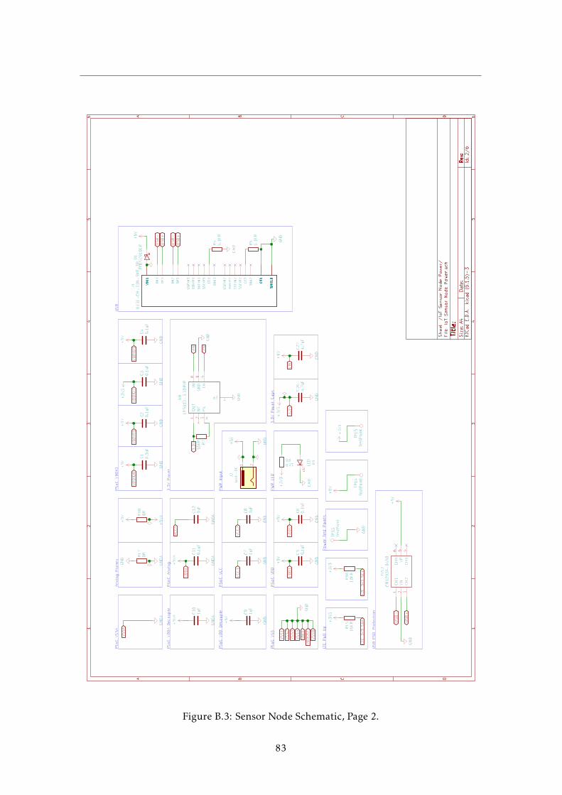
12
34
56
12
34
56
A B C D
A B C D
Dat
e:
KiC
ad E
.D.A
. ki
cad
(5.1
.5)-
3R
ev:
Siz
e: A
4Id
: 2/6
Tit
le:
File
: IoT
Sen
sor
Nod
e P
ower
.sch
She
et: /
IoT
Sen
sor
Nod
e P
ower
/
GN
DA
+5V
GN
DG
ND
GN
D
TP
15T
estP
oint
GN
D
GN
D
GN
D
GN
D
+3V
3
GN
D
GN
DA
GN
D
GN
DA
GN
DA
+5V
A
+3V
3
+5V
A
+5V
A
CH
11
VN
2
CH
23
CH
46
VP
5
CH
34
TV
S2
CM
1293
A-0
4SO
GN
DA
R61KR D
3LE
D
+3V
3
+5V
TP
14T
estP
oint
GN
D
+5V
TP
13T
estP
oint
C3
0.1u
F
GN
D
+3V
3
VB
US
VB
US
VB
US
VB
US
SH
IELD
SH
IELD
SH
IELD
SH
IELD
SH
IELD
SH
IELD
DN
1
DP
1
DN
2
DP
2
GN
DG
ND
GN
DG
ND
SS
RX
N1
SS
RX
P1
SS
TX
N1
SS
TX
P1
CC
1
SB
U1
SS
RX
N2
SS
RX
P2
SS
TX
N2
SS
TX
P2
CC
2
SB
U2
J1U
J31-
CH
-31N
-SM
T-T
R
R4
5.1K
R
R5
5.1K
R
R16
10K
R
R18
0R
+5V
+5V
+5V
+5V
+5V
+5V
+5V
GN
DG
ND
GN
D
GN
D
C7
1uF
D1
PM
EG
2010
ER
1 2
J2Ja
ck-D
C
C4
0.1u
FC
20.
1uF
C1
0.1u
F
C6
0.1u
FC
50.
1uF
C8
1uF
GN
D
C9
1uF
C12
1uF
C11
0.1u
FC
101u
F
+5V
OU
T1
NC
2
PG
3
EP 7
IN6
GN
D5
EN
4
U8
LP59
12-3
.3D
RV
R
GN
DR
710
KR
R17
0R
+3V
3
GN
D
R15
10K
R
C26
4.7u
FC
274.
7uF
+5V
GN
DG
ND
GN
D
+3V
3
I2C
_3V
3_S
DA
I2C
_3V
3_S
CL
US
B+
US
B-
VD
DIO
2
VB
OO
ST
VD
DIO
1
VS
S3
VS
S2
VS
S1
VD
D2
VD
D1
VC
C2
VC
C1
VD
DIO
3
VIN
VD
DIO
0
VC
CA
VD
DA
VS
SA
US
B-
US
B+
US
B-
US
B+
VB
AT
VS
S4
VS
SB
3.3V
VIN
VIN
3.3V
PS
oC A
nalo
gP
SoC
VD
DA
Dec
oupl
e
US
B E
SD
Pro
tect
ion
3.3V
Pow
er
US
B
PW
R In
put
Pow
er T
est P
oint
s
PS
oC V
DD
Dec
oupl
e
I2C
Pul
l Up
PS
oC V
DD
IO
PS
oC V
SS
PS
oC V
DD
PS
oC V
CC
PS
oC V
SS
AA
nalo
g P
lane
s
3.3V
Pow
er C
aps
PW
R L
ED
Figure B.3: Sensor Node Schematic, Page 2.
83
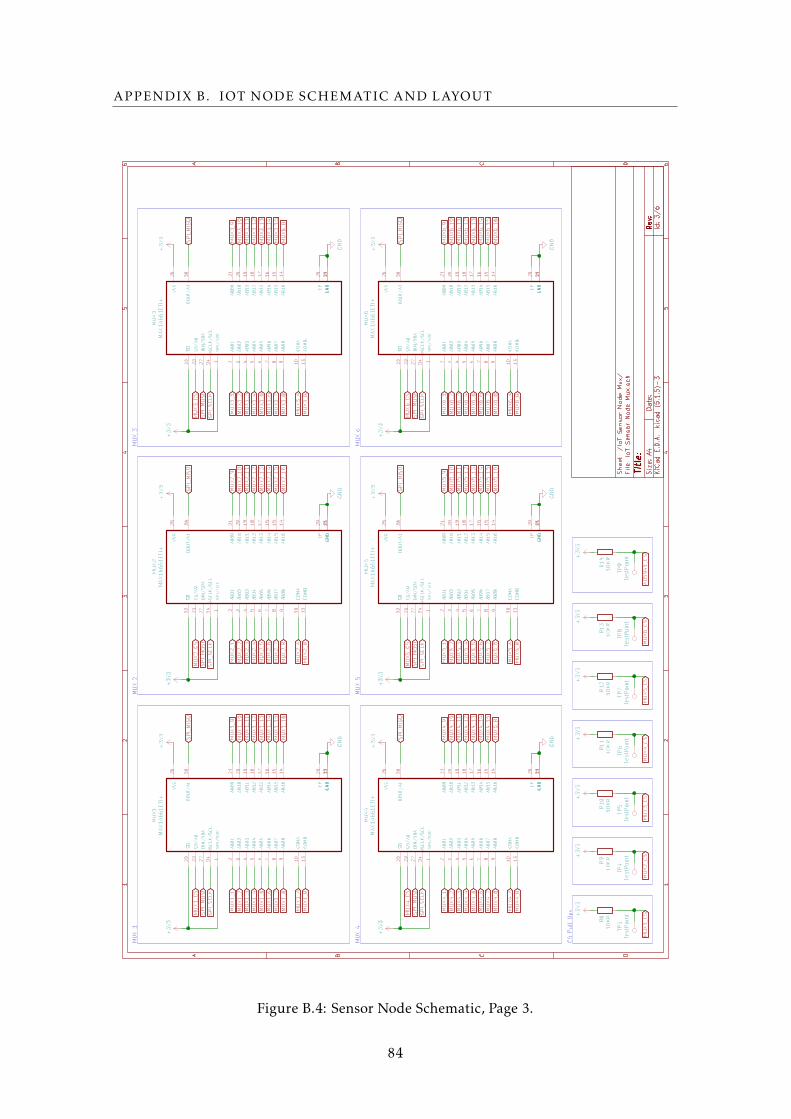
APPENDIX B. IOT NODE SCHEMATIC AND LAYOUT
12
34
56
12
34
56
A B C D
A B C D
Dat
e:
KiC
ad E
.D.A
. ki
cad
(5.1
.5)-
3R
ev:
Siz
e: A
4Id
: 3/6
Tit
le:
File
: IoT
Sen
sor
Nod
e M
ux.s
chS
heet
: /Io
T S
enso
r N
ode
Mux
/
+3V
3
R9
10K
RR
1010
KR
R11
10K
RR
1210
KR
R13
10K
RR
1410
KR
+3V
3+
3V3
+3V
3+
3V3
+3V
3+
3V3
+3V
3
TP
3T
estP
oint
TP
4T
estP
oint
TP
5T
estP
oint
TP
6T
estP
oint
TP
7T
estP
oint
TP
8T
estP
oint
TP
9T
estP
oint
+3V
3
+3V
3+
3V3
+3V
3+
3V3
GN
D
GN
DG
ND
+3V
3
GN
D
SD
22
CS
/A0
23
DIN
/SD
A27
SC
LK/S
CL
24
SP
I/!I2
C1
AB
012
AB
023
AB
034
AB
045
AB
056
AB
067
AB
078
AB
089
CO
MA
10
CO
MB
13
VC
C26
DO
UT
/A1
28
AB
0921
AB
1020
AB
1119
AB
1218
AB
1317
AB
1416
AB
1515
AB
1614
EP
29
GN
D11
GN
D25
MU
X1
MA
X14
661E
TI+
SD
22
CS
/A0
23
DIN
/SD
A27
SC
LK/S
CL
24
SP
I/!I2
C1
AB
012
AB
023
AB
034
AB
045
AB
056
AB
067
AB
078
AB
089
CO
MA
10
CO
MB
13
VC
C26
DO
UT
/A1
28
AB
0921
AB
1020
AB
1119
AB
1218
AB
1317
AB
1416
AB
1515
AB
1614
EP
29
GN
D11
GN
D25
MU
X2
MA
X14
661E
TI+
+3V
3
SD
22
CS
/A0
23
DIN
/SD
A27
SC
LK/S
CL
24
SP
I/!I2
C1
AB
012
AB
023
AB
034
AB
045
AB
056
AB
067
AB
078
AB
089
CO
MA
10
CO
MB
13
VC
C26
DO
UT
/A1
28
AB
0921
AB
1020
AB
1119
AB
1218
AB
1317
AB
1416
AB
1515
AB
1614
EP
29
GN
D11
GN
D25
MU
X3
MA
X14
661E
TI+
SD
22
CS
/A0
23
DIN
/SD
A27
SC
LK/S
CL
24
SP
I/!I2
C1
AB
012
AB
023
AB
034
AB
045
AB
056
AB
067
AB
078
AB
089
CO
MA
10
CO
MB
13
VC
C26
DO
UT
/A1
28
AB
0921
AB
1020
AB
1119
AB
1218
AB
1317
AB
1416
AB
1515
AB
1614
EP
29
GN
D11
GN
D25
MU
X4
MA
X14
661E
TI+
SD
22
CS
/A0
23
DIN
/SD
A27
SC
LK/S
CL
24
SP
I/!I2
C1
AB
012
AB
023
AB
034
AB
045
AB
056
AB
067
AB
078
AB
089
CO
MA
10
CO
MB
13
VC
C26
DO
UT
/A1
28
AB
0921
AB
1020
AB
1119
AB
1218
AB
1317
AB
1416
AB
1515
AB
1614
EP
29
GN
D11
GN
D25
MU
X5
MA
X14
661E
TI+
R8
10K
R
+3V
3
GN
DG
ND
+3V
3
SD
22
CS
/A0
23
DIN
/SD
A27
SC
LK/S
CL
24
SP
I/!I2
C1
AB
012
AB
023
AB
034
AB
045
AB
056
AB
067
AB
078
AB
089
CO
MA
10
CO
MB
13
VC
C26
DO
UT
/A1
28
AB
0921
AB
1020
AB
1119
AB
1218
AB
1317
AB
1416
AB
1515
AB
1614
EP
29
GN
D11
GN
D25
MU
X6
MA
X14
661E
TI+
+3V
3+
3V3
MU
X4_
3
MU
X1_
CS
MU
X2_
CS
MU
X3_
CS
MU
X4_
CS
MU
X5_
CS
MU
X6_
CS
AD
5941
_CS
MU
X2_
15
MU
X3_
3M
UX
3_2
MU
X3_
1
SP
I_M
ISO
SP
I_S
CLK
SP
I_M
OS
IM
UX
3_C
S
MU
X2_
16
MU
X3_
4
MU
X2_
14M
UX
2_13
MU
X2_
12M
UX
2_11
MU
X2_
10M
UX
2_9
MU
X2_
BM
UX
2_A
MU
X3_
10
SP
I_S
CLK
SP
I_M
OS
IM
UX
4_C
S
MU
X3_
15M
UX
3_14
MU
X3_
13M
UX
3_12
MU
X3_
11
MU
X2_
8
MU
X3_
9
MU
X3_
BM
UX
3_A
MU
X3_
8M
UX
3_7
MU
X3_
6M
UX
3_5
MU
X1_
5
MU
X1_
10M
UX
1_9
SP
I_M
ISO
MU
X1_
BM
UX
1_A
MU
X1_
8M
UX
1_7
MU
X1_
6
MU
X1_
11M
UX
1_4
MU
X1_
3M
UX
1_2
MU
X1_
1
SP
I_S
CLK
SP
I_M
OS
IM
UX
1_C
S
SP
I_S
CLK
MU
X2_
7M
UX
2_6
MU
X2_
5M
UX
2_4
MU
X2_
3M
UX
2_2
MU
X2_
1
SP
I_M
ISO
MU
X6_
B
SP
I_M
OS
IM
UX
2_C
S
MU
X1_
16M
UX
1_15
MU
X1_
14M
UX
1_13
MU
X1_
12
MU
X5_
12
SP
I_M
OS
I
MU
X6_
14
MU
X6_
CS
MU
X5_
16M
UX
5_15
MU
X5_
14M
UX
5_13
MU
X6_
15
SP
I_S
CLK
MU
X5_
11M
UX
5_10
MU
X5_
9
MU
X5_
B
MU
X6_
16
MU
X5_
A
MU
X5_
8M
UX
5_7
MU
X6_
6
MU
X6_
12M
UX
6_11
MU
X6_
10M
UX
6_9
MU
X6_
BM
UX
6_A
MU
X6_
8M
UX
6_7
MU
X5_
6M
UX
6_5
MU
X6_
4M
UX
6_3
MU
X6_
13
MU
X6_
2M
UX
6_1
SP
I_M
ISO
MU
X4_
11
MU
X4_
1M
UX
4_2
MU
X4_
4M
UX
4_5
MU
X4_
6M
UX
4_7
MU
X4_
8
MU
X4_
AM
UX
4_B
SP
I_M
ISO
MU
X4_
9M
UX
4_10
MU
X4_
12M
UX
4_13
SP
I_M
ISO
MU
X5_
5
MU
X5_
B
MU
X5_
4M
UX
5_3
MU
X5_
2M
UX
5_1
SP
I_S
CLK
MU
X4_
14
SP
I_M
OS
IM
UX
5_C
S
MU
X4_
15
MU
X 4
MU
X 1
MU
X 5
MU
X 6
MU
X 3
CS
Pul
l Ups
MU
X 2
Figure B.4: Sensor Node Schematic, Page 3.
84
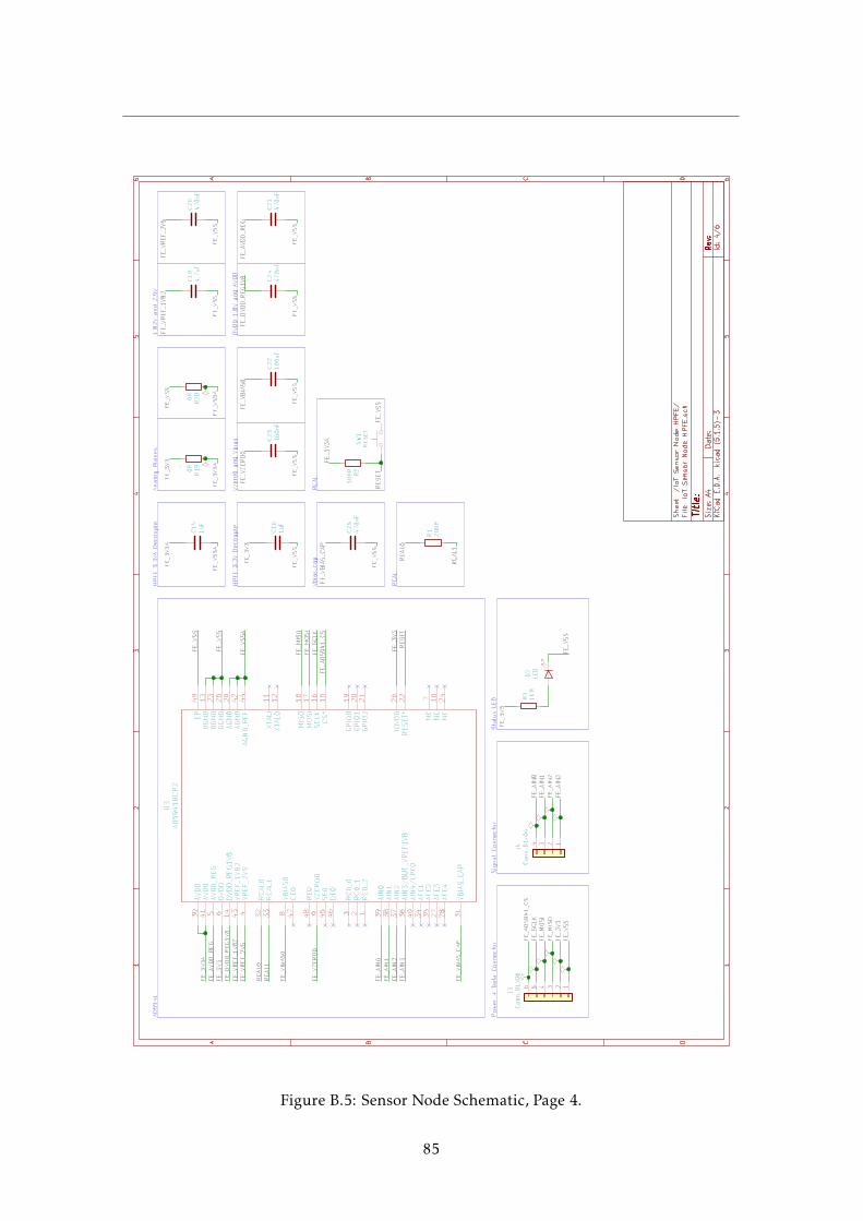
12
34
56
12
34
56
A B C D
A B C D
Dat
e:
KiC
ad E
.D.A
. ki
cad
(5.1
.5)-
3R
ev:
Siz
e: A
4Id
: 4/6
Tit
le:
File
: IoT
Sen
sor
Nod
e H
PF
E.s
chS
heet
: /Io
T S
enso
r N
ode
HP
FE
/
C24
470n
F
C20
470n
F
C25
470n
F
C22
100n
F
D2
LED
RC
0_2
1R
C0_
12
RC
0_0
3
VR
EF
_2V
54
AV
DD
_RE
G5
DV
DD
6
NC
7
VB
IAS
08
VZ
ER
O0
9
NC
10
XT
ALI
11
XT
ALO
12
DG
ND
13
DV
DD
_RE
G1V
814
CS
*15
SC
LK16
MO
SI
17M
ISO
18
GP
IO0
19
GP
IO1
20
GP
IO2
21
RE
SE
T*
22
DG
ND
23
NC
24
DG
ND
25
IOV
DD
26
AF
E3
27
AF
E4
28
AG
ND
29
AV
DD
30
VB
IAS
_CA
P31
RC
AL0
32
RC
AL1
33
AF
E1
34
AF
E2
35
AIN
3/B
UF
_VR
EF
1V8
36A
IN2
37A
IN1
38A
IN0
39
AIN
4/LP
F0
40
AV
DD
41
AG
ND
42V
RE
F_1
V82
43
AG
ND
_RE
F44
SE
045
DE
046
CE
047
RE
048
EP
49
U3
AD
5941
BC
PZ
C16
1uF
C15
1uF
C23
100n
F
R2
10K
R
C19
4.7u
F
C21
470n
F
R200R
1234
J4C
onn_
01x0
4
R1
200R
R190R
SW
1R
ES
ET
123456
J3C
onn_
01x0
6R
31K
R
FE
_VR
EF
_2V
5
RE
SE
T
FE
_AD
5941
_CS
FE
_3V
3
FE
_VB
IAS
0
RE
SE
T
FE
_VS
S
FE
_VS
S
FE
_3V
3A
FE
_VR
EF
_1V
82F
E_D
VD
D_R
EG
1V8
FE
_3V
3F
E_A
VD
D_R
EG
FE
_VZ
ER
O0
FE
_AIN
1F
E_A
IN2
FE
_AIN
3
FE
_MO
SI
RC
AL1
FE
_VS
S
RC
AL0
FE
_VB
IAS
_CA
P
FE
_AIN
0
FE
_3V
3A
FE
_VS
S
FE
_SC
LK
FE
_MIS
O
FE
_MO
SI
FE
_3V
3
FE
_VS
SA
FE
_VS
SA
FE
_VZ
ER
O0
FE
_VS
SF
E_3
V3
FE
_VB
IAS
_CA
P
FE
_3V
3
FE
_3V
3A
FE
_AD
5941
_CS
FE
_SC
LK
FE
_MIS
O
RC
AL1
RC
AL0
FE
_VS
S
FE
_VB
IAS
0
FE
_VS
SF
E_V
SS
FE
_VS
S
FE
_VS
SF
E_V
SS
FE
_VS
SF
E_V
SS
FE
_VS
SF
E_3
V3
FE
_VS
SA
FE
_3V
3A
FE
_AV
DD
_RE
G
FE
_AIN
3
FE
_AIN
0F
E_A
IN1
FE
_AIN
2
FE
_VR
EF
_1V
82F
E_V
RE
F_2
V5
FE
_DV
DD
_RE
G1V
8
Vbi
as_c
ap
Vze
ro0
and
Vbi
as
RC
AL
DV
DD
1.8
V a
nd A
VD
D
Sig
nal C
onne
ctor
AD
5941
RC
AL
HP
FE
3.3
V D
ecou
ple
Pow
er +
Dat
a C
onne
ctor
HP
FE
3.3
VA
Dec
oupl
e1.
82V
and
2.5
V
Sta
tus
LED
Ana
log
Pla
nes
Figure B.5: Sensor Node Schematic, Page 4.
85

APPENDIX B. IOT NODE SCHEMATIC AND LAYOUT
12
34
56
12
34
56
A B C D
A B C D
Dat
e:
KiC
ad E
.D.A
. ki
cad
(5.1
.5)-
3R
ev:
Siz
e: A
4Id
: 5/6
Tit
le:
File
: IoT
Sen
sor
Nod
e R
F.s
chS
heet
: /Io
T S
enso
r N
ode
RF
/
+5V
GN
D
GN
D
C29
33pF
GN
D
C30
33pF
GN
D
C28
0.1u
FC
3133
pF
GN
D
GN
D
C32
33pF
VC
CC
1
RS
TC
2
CLK
C3
GN
DC
5
VP
PC
6
I/OC
7
CS
W1
CS
W1
DS
W1
DS
W1
GN
D1
GN
D1
GN
D2
GN
D2
GN
D3
GN
D3
GN
D4
GN
D4
GN
D5
GN
D5
GN
D6
GN
D6
GN
D7
GN
D7
GN
D8
GN
D8
GN
D9
GN
D9
GN
D10
GN
D10
SIM
1S
F72
S00
6VB
AR
2500
CH
11
VN
2
CH
23
CH
46
VP
5
CH
34
TV
S1
CM
1293
A-0
4SO
GN
D
GN
D
TP
1T
estP
oint
TP
2T
estP
oint
+3V
3
GN
D
C33
100u
FC
340.
1uF
C35
10nF
C36
68pF
C37
15pF
TP
10T
estP
oint
TP
11T
estP
oint
TP
12T
estP
oint
1
2
AN
T1
Con
n_C
oaxi
al
GN
D
GN
D1
GN
D3
GN
D5
GN
D14
GN
D20
GN
D21
GN
D22
GN
D30
GN
D32
GN
D43
GN
D50
GN
D54
GN
D55
GN
D57
GN
D58
GN
D59
GN
D60
GN
D61
GN
D63
GN
D64
GN
D65
GN
D66
GN
D67
GN
D68
GN
D69
GN
D70
GN
D71
GN
D72
GN
D73
GN
D74
GN
D75
GN
D76
GN
D77
GN
D78
GN
D79
GN
D80
GN
D81
GN
D82
GN
D83
GN
D84
GN
D85
GN
D86
GN
D87
GN
D88
GN
D89
GN
D90
GN
D91
GN
D92
GN
D93
GN
D94
GN
D95
GN
D96
V_I
NT
4
RT
S10
CT
S11
TX
D12
RX
D13
GP
IO1
16
RE
SE
T_N
18
GP
IO2
24S
DA
26S
CL
27
RS
VD
_33
33
RS
VD
_31
31
SIM
_CLK
38
SIM
_IO
39
SIM
_RS
T40
VS
IM41
VC
C51
VC
C52
VC
C53
AN
T56
AN
T_D
ET
62
U2
SA
RA
-N21
0S
AR
A_V
SIM TV
S1_
CH
1
SA
RA
_SIM
_CLK
SA
RA
_SIM
_RS
TS
AR
A_S
IM_I
OS
AR
A_S
IM_I
O
SA
RA
_VS
IM
TVS1_CH3
SA
RA
_SIM
_CLK
SA
RA
_SIM
_IO
TV
S1_
CH
4
SA
RA
_SIM
_RS
T
TV
S1_
CH
3
TVS1_CH1
TV
S1_
CH
2
SA
RA
_SIM
_RS
T
TVS1_CH2
SA
RA
_AN
T
SA
RA
_TX
DS
AR
A_R
XD
SA
RA
_CT
S
SA
RA
_RE
SE
T
SA
RA
_VIN
SA
RA
_VIN
SA
RA
_VS
IM
SA
RA
_AN
T
SA
RA
_SIM
_CLK
TVS1_CH4
ES
D P
rote
ctio
n
ES
D P
rote
ctio
n
ES
D P
rote
ctio
n
Ant
enna
Con
nect
or
nano
SIM
Car
d S
lot
ublo
x S
AR
A N
210
ES
D P
rote
ctio
n
SIM
ES
D P
rote
ctio
n
SA
RA
Inpu
t Cap
acito
rs
Figure B.6: Sensor Node Schematic, Page 5.
86
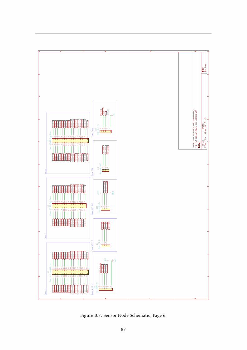
12
34
56
12
34
56
A B C D
A B C D
Dat
e:
KiC
ad E
.D.A
. ki
cad
(5.1
.5)-
3R
ev:
Siz
e: A
4Id
: 6/6
Tit
le:
File
: IoT
Sen
sor
Nod
e C
onne
ctor
s.sc
hS
heet
: /Io
T S
enso
r N
ode
Con
nect
ors/
1
1011
1213
1415
1617
1819
2 2021
2223
2425
2627
28293
3031
3245
67
89
J7C
onn_
02x1
6_O
dd_E
ven
123
J11
Con
n_01
x03
GN
D
+3V
3
1
1011
1213
1415
1617
1819
2 2021
2223
2425
2627
28293
3031
3245
67
89
J5C
onn_
02x1
6_O
dd_E
ven
123456
J8C
onn_
01x0
6
1234
J9C
onn_
01x0
4
1234
J10
Con
n_01
x04
12345
J12
Con
n_01
x05
1
1011
1213
1415
1617
1819
2 2021
2223
2425
2627
28293
3045
67
89
J6C
onn_
02x1
5_O
dd_E
ven
+5V
GN
D
+3V
3
GN
D
SW
DC
LKS
WD
IO
RS
TS
PI_
MIS
OS
PI_
MO
SI
SP
I_S
CLK
MU
X1_
3
I2C
_3V
3_S
DA
I2C
_3V
3_S
CL
MU
X1_
1
MU
X4_
3
MU
X2_
16
MU
X3_
1M
UX
3_2
MU
X1_
6
MU
X3_
3M
UX
3_4
MU
X3_
5M
UX
3_6
MU
X3_
7M
UX
3_8
MU
X4_
1M
UX
4_2
MU
X2_
15
MU
X4_
4M
UX
4_5
MU
X4_
6M
UX
4_7
MU
X4_
8
MU
X4_
9M
UX
4_10
MU
X4_
11M
UX
4_12
MU
X4_
13M
UX
4_14
MU
X4_
15
MU
X2_
3
MU
X1_
8
MU
X1_
9M
UX
1_10
MU
X1_
11M
UX
1_12
MU
X1_
13M
UX
1_14
MU
X1_
15M
UX
1_16
MU
X2_
1
MU
X1_
7
MU
X2_
2M
UX
5_1
MU
X2_
4M
UX
2_5
MU
X2_
6M
UX
2_7
MU
X2_
8
MU
X2_
9M
UX
2_10
MU
X2_
11M
UX
2_12
MU
X2_
13M
UX
2_14
MU
X3_
9M
UX
6_11
MU
X6_
12M
UX
6_13
MU
X6_
14M
UX
6_15
MU
X6_
16M
UX
3_15
MU
X3_
14M
UX
3_13
MU
X3_
12M
UX
3_11
MU
X3_
10
MU
X5_
2
MU
X1_
5M
UX
1_4
MU
X1_
2
AD
5941
_CS
SP
I_S
CLK
SP
I_M
OS
IS
PI_
MIS
O
MU
X1_
BM
UX
2_B
MU
X3_
BM
UX
4_B
MU
X6_
9
MU
X5_
3M
UX
5_4
MU
X5_
5M
UX
5_6
MU
X5_
7M
UX
5_8
MU
X5_
9M
UX
5_10
MU
X5_
11M
UX
5_12
MU
X5_
13M
UX
5_14
MU
X5_
15M
UX
5_16
MU
X6_
1M
UX
6_2
MU
X6_
3M
UX
6_4
MU
X6_
5M
UX
6_6
MU
X6_
7M
UX
6_8
MU
X6_
10
Con
n P
rog
Con
n H
PF
E 2
Con
n S
PI
Con
n I2
C 3
V3
Con
n 1
Con
n 2
Con
n 3
Con
n H
PF
E 1
Figure B.7: Sensor Node Schematic, Page 6.
87
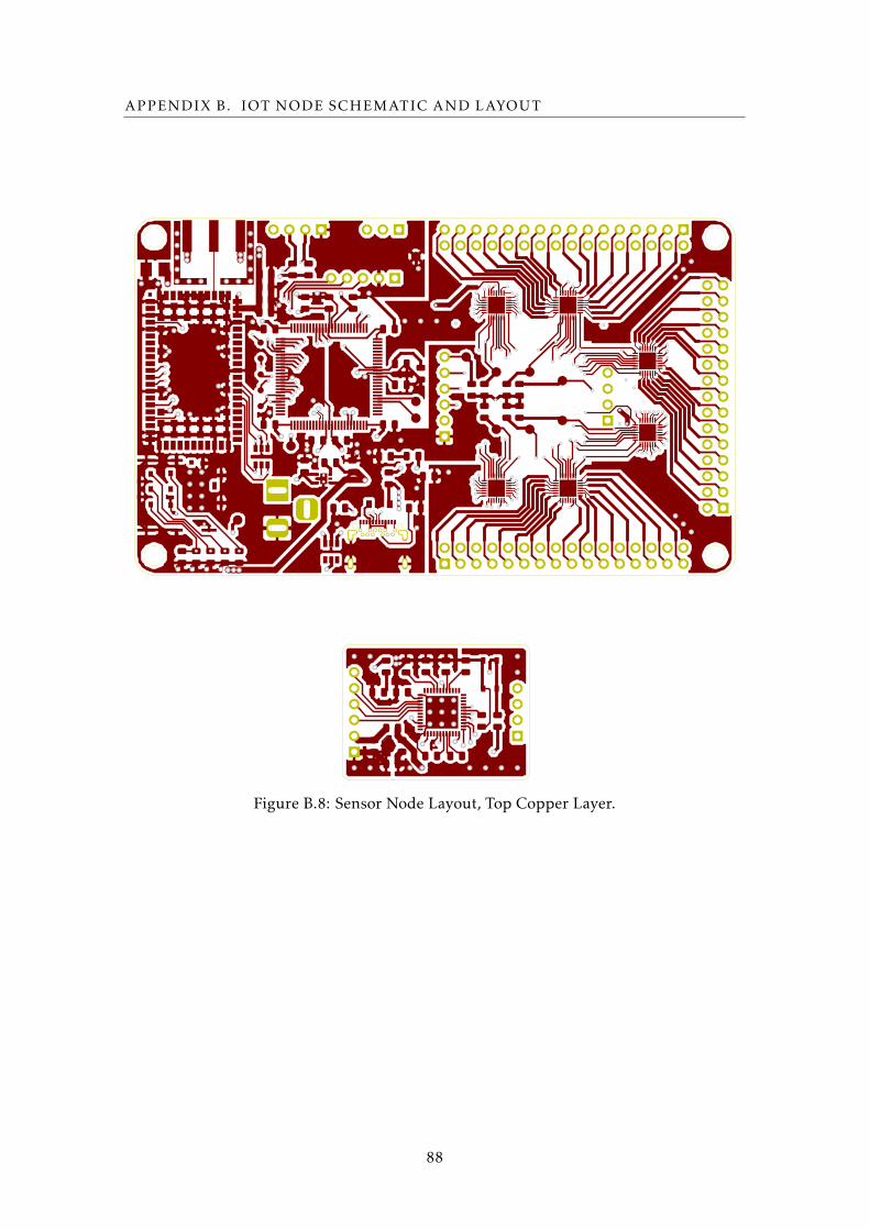
APPENDIX B. IOT NODE SCHEMATIC AND LAYOUT
Figure B.8: Sensor Node Layout, Top Copper Layer.
88

Figure B.9: Sensor Node Schematic, First Inside Copper Layer.
89
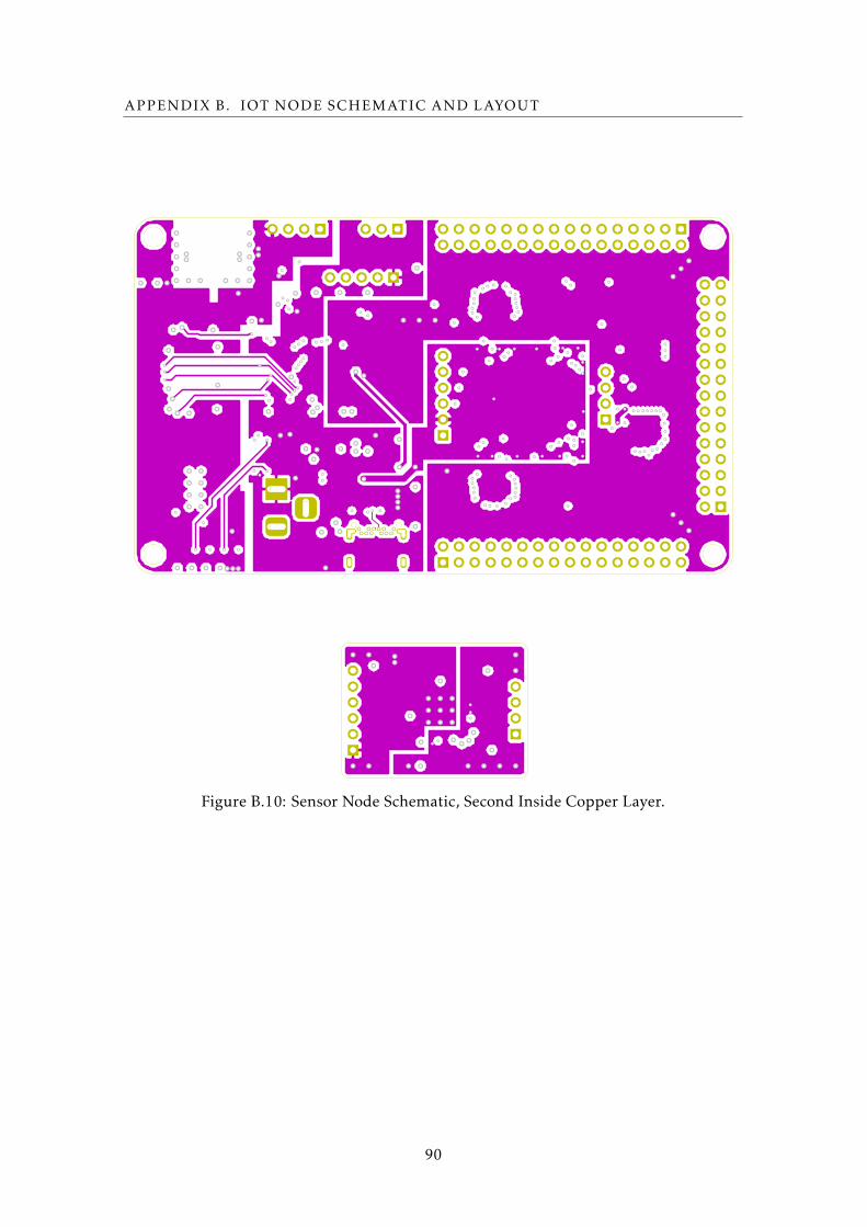
APPENDIX B. IOT NODE SCHEMATIC AND LAYOUT
Figure B.10: Sensor Node Schematic, Second Inside Copper Layer.
90

Figure B.11: Sensor Node Schematic, Bottom Copper Layer.
91
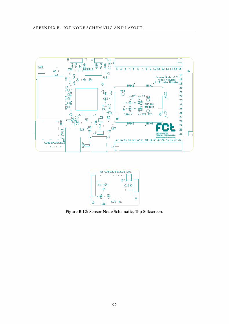
APPENDIX B. IOT NODE SCHEMATIC AND LAYOUT
Figure B.12: Sensor Node Schematic, Top Silkscreen.
92

Figure B.13: Sensor Node Schematic, Bottom Silkscreen.
93

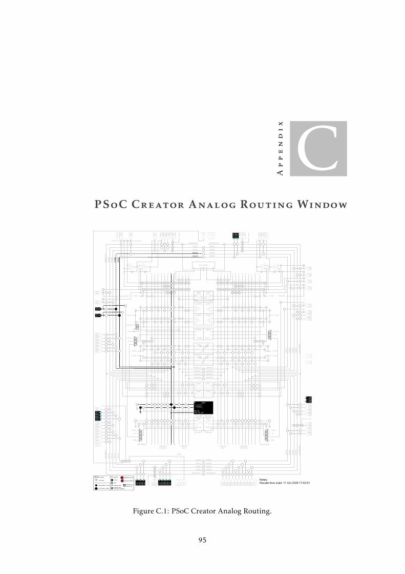
Appendix
CPSoC Creator Analog Routing Window
Figure C.1: PSoC Creator Analog Routing.
95


Appendix
DMATLAB Script for Sampled Data
Processing
1 c l e a r a l l
2 c l o s e a l l
3
4 t i c
5 fo r c = 1:11
6 switch c
7 case 1
8 data = csvread ( ’ 20b_ds_mst_92_bg2_5k . csv ’ ) ;
9 data ( : , 2 ) = [ ] ;
10 n = 0 . 5 ;
11 l s b = 1.024 / 2^21 * 10^6;
12 f i g u r e ( c )
13 s g t i t l e ( ’ 20−b i t DelSig ADC, Multi Sample ( Turbo ) , SR = 92 SPS ,
Buf . Gain = 2 , 5.000 Samples per Measurement ’ , ’ ’ , ’ FontSize ’ , 28) ;
14 case 2
15 data = csvread ( ’ 20b_ds_mst_182_bg1_5k . csv ’ ) ;
16 data ( : , 2 ) = [ ] ;
17 n = 0 . 5 ;
18 l s b = 1.024 / 2^20 * 10^6;
19 f i g u r e ( c )
20 s g t i t l e ( ’ 20−b i t DelSig ADC, Multi Sample ( Turbo ) , SR = 182 SPS ,
Buf . Gain = 1 , 5.000 Samples per Measurement ’ , ’ ’ , ’ FontSize ’ , 28) ;
21 case 3
22 data = csvread ( ’ 18b_ds_mst_1238_bg2_10k . csv ’ ) ;
23 data ( : , 2 ) = [ ] ;
24 n = 1 ;
25 l s b = 1.024 / 2^19 * 10^6;
26 f i g u r e ( c )
97
APPENDIX D. MATLAB SCRIPT FOR SAMPLED DATA PROCESSING
27 s g t i t l e ( ’ 18−b i t DelSig ADC, Multi Sample ( Turbo ) , SR = 1238 SPS ,
Buf . Gain = 2 , 10.000 Samples per Measurement ’ , ’ ’ , ’ FontSize ’ , 28) ;
28 case 4
29 data = csvread ( ’ 18b_ds_mst_2477_bg1_10k . csv ’ ) ;
30 data ( : , 2 ) = [ ] ;
31 n = 1 ;
32 l s b = 1.024 / 2^18 * 10^6;
33 f i g u r e ( c )
34 s g t i t l e ( ’ 18−b i t DelSig ADC, Multi Sample ( Turbo ) , SR = 2477 SPS ,
Buf . Gain = 1 , 10.000 Samples per Measurement ’ , ’ ’ , ’ FontSize ’ , 28) ;
35 case 5
36 data = csvread ( ’ 16b_ds_mst_5505_bg2_20k . csv ’ ) ;
37 data ( : , 2 ) = [ ] ;
38 n = 2 ;
39 l s b = 1.024 / 2^17 * 10^6;
40 f i g u r e ( c )
41 s g t i t l e ( ’ 16−b i t DelSig ADC, Multi Sample ( Turbo ) , SR = 5505 SPS ,
Buf . Gain = 2 , 20.000 Samples per Measurement ’ , ’ ’ , ’ FontSize ’ , 28) ;
42 case 6
43 data = csvread ( ’ 16b_ds_mst_11010_bg1_20k . csv ’ ) ;
44 data ( : , 2 ) = [ ] ;
45 n = 2 ;
46 l s b = 1.024 / 2^16 * 10^6;
47 f i g u r e ( c )
48 s g t i t l e ( ’ 16−b i t DelSig ADC, Multi Sample ( Turbo ) , SR = 11010 SPS ,
Buf . Gain = 1 , 20.000 Samples per Measurement ’ , ’ ’ , ’ FontSize ’ , 28) ;
49 case 7
50 data = csvread ( ’ 14b_ds_mst_14840_bg2_20k . csv ’ ) ;
51 data ( : , 2 ) = [ ] ;
52 n = 2 ;
53 l s b = 1.024 / 2^15 * 10^6;
54 f i g u r e ( c )
55 s g t i t l e ( ’ 14−b i t DelSig ADC, Multi Sample ( Turbo ) , SR = 14840 SPS ,
Buf . Gain = 2 , 20.000 Samples per Measurement ’ , ’ ’ , ’ FontSize ’ , 28) ;
56 case 8
57 data = csvread ( ’ 14b_ds_mst_29681_bg1_20k . csv ’ ) ;
58 data ( : , 2 ) = [ ] ;
59 n = 2 ;
60 l s b = 1.024 / 2^14 * 10^6;
61 f i g u r e ( c )
62 s g t i t l e ( ’ 14−b i t DelSig ADC, Multi Sample ( Turbo ) , SR = 29681 SPS ,
Buf . Gain = 1 , 20.000 Samples per Measurement ’ , ’ ’ , ’ FontSize ’ , 28) ;
63 case 9
64 data = csvread ( ’ 20b_ds_mst_182_bg1_5k_high . csv ’ ) ;
65 data ( : , 2 ) = [ ] ;
66 n = 0 . 5 ;
67 l s b = 1.024 / 2^20 * 10^6;
68 f i g u r e ( c )
98

69 s g t i t l e ( ’ High value r e s i s t o r s , 20−b i t DelSig ADC, Multi Sample (
Turbo ) , SR = 182 SPS , Buf . Gain = 1 , 5.000 Samples per Measurement ’ , ’ ’ ,
’ FontSize ’ , 28) ;
70 case 10
71 data = csvread ( ’ 18b_ds_mst_2477_bg1_10k_high . csv ’ ) ;
72 data ( : , 2 ) = [ ] ;
73 n = 1 ;
74 l s b = 1.024 / 2^18 * 10^6;
75 f i g u r e ( c )
76 s g t i t l e ( ’ High value r e s i s t o r s , 18−b i t DelSig ADC, Multi Sample (
Turbo ) , SR = 2477 SPS , Buf . Gain = 1 , 10.000 Samples per Measurement ’ , ’ ’
, ’ FontSize ’ , 28) ;
77 case 11
78 data = csvread ( ’ 16b_ds_mst_11010_bg1_20k_high . csv ’ ) ;
79 data ( : , 2 ) = [ ] ;
80 n = 2 ;
81 l s b = 1.024 / 2^16 * 10^6;
82 f i g u r e ( c )
83 s g t i t l e ( ’ High value r e s i s t o r s , 16−b i t DelSig ADC, Multi Sample (
Turbo ) , SR = 11010 SPS , Buf . Gain = 1 , 20.000 Samples per Measurement ’ , ’ ’
, ’ FontSize ’ , 28) ;
84 end
85
86 setGlobala ( 1 ) ;
87 s e t ( gcf , ’ P o s i t i o n ’ , [100 , 100 , 1600 , 900] )
88
89 data_1u_22r = data ( 1 : ( n * 10000) ) ;
90 data_1u_465r = data ( ( 1 + n * 10000) : ( n * 20000) ) ;
91 data_1u_992r = data ( ( 1 + n * 20000) : ( n * 30000) ) ;
92
93 data_10u_22r = data ( ( 1 + n * 30000) : ( n * 40000) ) ;
94 data_10u_465r = data ( ( 1 + n * 40000) : ( n * 50000) ) ;
95 data_10u_992r = data ( ( 1 + n * 50000) : ( n * 60000) ) ;
96
97 data_100u_22r = data ( ( 1 + n * 60000) : ( n * 70000) ) ;
98 data_100u_465r = data ( ( 1 + n * 70000) : ( n * 80000) ) ;
99 data_100u_992r = data ( ( 1 + n * 80000) : ( n * 90000) ) ;
100
101 [ n1 , n991 , m1, s1 , nlsb1 ] = process ( data_1u_22r , lsb , 22 , 1) ;
102 [ n2 , n992 , m2, s2 , nlsb2 ] = process ( data_1u_465r , lsb , 465 , 1) ;
103 [ n3 , n993 , m3, s3 , nlsb3 ] = process ( data_1u_992r , lsb , 992 , 1) ;
104 [ n4 , n994 , m4, s4 , nlsb4 ] = process ( data_10u_22r , lsb , 22 , 10) ;
105 [ n5 , n995 , m5, s5 , nlsb5 ] = process ( data_10u_465r , lsb , 465 , 10) ;
106 [ n6 , n996 , m6, s6 , nlsb6 ] = process ( data_10u_992r , lsb , 992 , 10) ;
107 [ n7 , n997 , m7, s7 , nlsb7 ] = process ( data_100u_22r , lsb , 22 , 100) ;
108 [ n8 , n998 , m8, s8 , nlsb8 ] = process ( data_100u_465r , lsb , 465 , 100) ;
109 [ n9 , n999 , m9, s9 , nlsb9 ] = process ( data_100u_992r , lsb , 992 , 100) ;
110
111 m4 = m4 / 10; m5 = m5 / 10; m6 = m6 / 10;
112 s4 = s4 / 10; s5 = s5 / 10; s6 = s6 / 10;
99
APPENDIX D. MATLAB SCRIPT FOR SAMPLED DATA PROCESSING
113
114 m7 = m7 / 100; m8 = m8 / 100; m9 = m9 / 100;
115 s7 = s7 / 100; s8 = s8 / 100; s9 = s9 / 100;
116
117 % f i g u r e ( 1 ) ;
118
119 subplot ( 1 , 3 , 1 )
120 x1 = [m1,m4,m7 ] ;
121 y1 = 1 : 3 ;
122 bar ( y1 , x1 , ’ FaceColor ’ , [ 0 . 2 5 , 0 .25 , 0 . 2 5 ] )
123 x t i c k l a b e l s ( ’ 1\mu’ , ’ 10\mu’ , ’ 100\mu’ )
124 i f ( c < 9)
125 t i t l e ( ’ 22\Omega R e s i s t o r ’ , ’ ( Measured at 21.7\Omega) ’ , ’ FontSize ’ ,
18)
126 end
127 i f ( c > 8)
128 t i t l e ( ’ 3 .3K\Omega R e s i s t o r ’ , ’ ( Measured at 3.28K\Omega) ’ , ’ FontSize
’ , 18)
129 end
130 ylim ( [ 0 5 0 ] ) ;
131 errlow = [2* s1 2* s4 2* s7 ] ;
132 errhigh = [2* s1 2* s4 2* s7 ] ;
133 hold on
134 ax = plot ( xlim , [ 2 1 . 7 2 1 . 7 ] , ’ LineWidth ’ , 2) ;
135 ax . Color = [ 0 , 0.4470 0 . 7 4 1 0 ] ;
136 er = errorbar ( y1 , x1 , errlow , errhigh ) ;
137 er . Color = ’ r ’ ;
138 er . L ineSty le = ’ none ’ ;
139 er . LineWidth = 2 ;
140 hold o f f
141 x l a b e l ( ’ P o l a r i z a t i o n Current (A) ’ , ’ FontSize ’ , 16) ;
142 y l a b e l ( ’ Measured R e s i s t o r Value (\Omega) ’ , ’ FontSize ’ , 16) ;
143 ax = gca ;
144 ax . XAxis . FontSize = 16;
145 ax . YAxis . FontSize = 16;
146
147 subplot ( 1 , 3 , 2 )
148 x2 = [m2,m5,m8 ] ;
149 bar ( y1 , x2 , ’ FaceColor ’ , [ 0 . 2 5 , 0 .25 , 0 . 2 5 ] ) ;
150 x t i c k l a b e l s ( ’ 1\mu’ , ’ 10\mu’ , ’ 100\mu’ )
151 i f ( c < 9)
152 t i t l e ( ’ 470\Omega R e s i s t o r ’ , ’ ( Measured at 465\Omega) ’ , ’ FontSize ’ ,
18)
153 end
154 i f ( c > 8)
155 t i t l e ( ’ 6 .8K\Omega R e s i s t o r ’ , ’ ( Measured at 6.76K\Omega) ’ , ’ FontSize
’ , 18)
156 end
157 ylim ( [ 0 600] ) ;
158 errlow = [2* s2 2* s5 2* s8 ] ;
100
159 errhigh = [2* s2 2* s5 2* s8 ] ;
160 hold on
161 ax = plot ( xlim , [ 4 6 5 465] , ’ LineWidth ’ , 2) ;
162 ax . Color = [ 0 , 0.4470 0 . 7 4 1 0 ] ;
163 er = errorbar ( y1 , x2 , errlow , errhigh ) ;
164 er . Color = ’ r ’ ;
165 er . L ineSty le = ’ none ’ ;
166 er . LineWidth = 2 ;
167 hold o f f
168 x l a b e l ( ’ P o l a r i z a t i o n Current (A) ’ , ’ FontSize ’ , 16) ;
169 y l a b e l ( ’ Measured R e s i s t o r Value (\Omega) ’ , ’ FontSize ’ , 16) ;
170 ax = gca ;
171 ax . XAxis . FontSize = 16;
172 ax . YAxis . FontSize = 16;
173
174 subplot ( 1 , 3 , 3 )
175 x3 = [m3,m6,m9 ] ;
176 bar ( y1 , x3 , ’ FaceColor ’ , [ 0 . 2 5 , 0 .25 , 0 . 2 5 ] )
177 x t i c k l a b e l s ( ’ 1\mu’ , ’ 10\mu’ , ’ 100\mu’ )
178 i f ( c < 9)
179 t i t l e ( ’ 1K\Omega R e s i s t o r ’ , ’ ( Measured at 992\Omega) ’ , ’ FontSize ’ ,
18)
180 end
181 i f ( c > 8)
182 t i t l e ( ’ 10K\Omega R e s i s t o r ’ , ’ ( Measured at 9.90K\Omega) ’ , ’ FontSize ’
, 18)
183 end
184 ylim ( [ 0 1200]) ;
185 errlow = [2* s3 2* s6 2* s9 ] ;
186 errhigh = [2* s3 2* s6 2* s9 ] ;
187 hold on
188 ax = plot ( xlim , [ 9 9 2 992] , ’ LineWidth ’ , 2) ;
189 ax . Color = [ 0 , 0.4470 0 . 7 4 1 0 ] ;
190 er = errorbar ( y1 , x3 , errlow , errhigh ) ;
191 er . Color = ’ r ’ ;
192 er . L ineSty le = ’ none ’ ;
193 er . LineWidth = 2 ;
194 hold o f f
195 x l a b e l ( ’ P o l a r i z a t i o n Current (A) ’ , ’ FontSize ’ , 16) ;
196 y l a b e l ( ’ Measured R e s i s t o r Value (\Omega) ’ , ’ FontSize ’ , 16) ;
197 ax = gca ;
198 ax . XAxis . FontSize = 16;
199 ax . YAxis . FontSize = 16;
200
201 f igHandles = f i n d a l l ( 0 , ’ Type ’ , ’ f i g u r e ’ ) ;
202
203 syms f i g _ b i t ;
204 eqn = 2 == nthroot ( l sb * 10^(−6) , f i g _ b i t ) ;
205 b i t s = so lve ( eqn , f i g _ b i t ) ;
206 b i t s = abs ( round ( b i t s ) ) ;
101
APPENDIX D. MATLAB SCRIPT FOR SAMPLED DATA PROCESSING
207
208 b i t s = double ( b i t s ) ;
209 t ex t3 = [ num2str ( b i t s ) , ’ b i t s ’ ] ;
210 fn = tex t3 ;
211
212
213 % e x p o r t _ f i g ( fn , ’−pdf ’ , f igHandles ( 1 ) )
214 % for i = numel ( f igHandles ) : −1:2
215 % e x p o r t _ f i g ( fn , ’−pdf ’ , f igHandles ( i ) , ’−append ’ )
216 % end
217
218 end
219 toc
220
221 funct ion [ noise , noise99 , m, s , nlsb ] = process ( x , lsb , r , curr )
222 n = length ( x ) ;
223 noise = max( x )−min ( x ) ;
224 m = sum( x ) /n ;
225 s = std ( x ) ;
226 noise99 = 6 * s ;
227 nlsb = s / l s b ;
228
229 t b l = t a b u l a t e ( x ) ;
230 i n d i c e s = t b l ( : , 2 ) == 0 ;
231 t b l ( indices , : ) = [ ] ;
232
233 t b l ( a l l (~ tbl , 2 ) , : ) = [ ] ; %rows
234 t b l ( : , a l l (~x , 1 ) ) = [ ] ; %columns
235
236 t b l = num2cell ( t b l ) ;
237 t = c e l l 2 t a b l e ( tbl , ’ VariableNames ’ , ’ Value ’ , ’ Count ’ , ’ Percent ’ ) ;
238 t . Value = c a t e g o r i c a l ( t . Value ) ;
239
240
241 % a = getGlobala ;
242 % s e t ( 0 , ’ DefaultAxesTitleFontWeight ’ , ’ normal ’ ) ;
243 % f i g u r e ( a +1) ;
244 % bar ( t . Value , t . Count )
245 % s e t ( gcf , ’ P o s i t i o n ’ , [100 , 100 , 1600 , 900] )
246 % y l a b e l ( ’Number of Samples ’ , ’ FontSize ’ , 16) ;
247 % x l a b e l ( ’ Measured Voltage (\muV) ’ , ’ FontSize ’ , 16) ;
248 % t e x t = [ ’ 99.7% Noise = ’ , num2str ( noise99 ) , ’ \muV, RMS Noise = ’ ,
num2str ( s ) , ’ \muV ( ’ , num2str ( nlsb ) , ’ LSB ) ’ ] ;
249 % text2 = [ ’ Pol . Current = ’ , num2str ( curr ) , ’ \muA , R e s i s t o r Value = ’ ,
num2str ( r ) , ’ \Omega ’ ] ;
250 % t i t l e ( text , text2 , ’ ’ , ’ FontSize ’ , 28) ;
251 %
252 % a = a + 1 ;
253 % setGlobala ( a ) ;
254
102
255
256 end
257
258 funct ion setGlobala ( val )
259 global a
260 a = val ;
261 end
262
263 funct ion r = getGlobala
264 global a
265 r = a ;
266 end
Listing D.1: MATLAB Script
103