A Single-Transistor Class C Amplifier 50 Watts Output for 30m CW
23
A Single-Transistor Class C Amplifier 50 Watts Output for 30m CW Stephen E. Sussman-Fort, Ph.D. AB2EW [email protected]
Transcript of A Single-Transistor Class C Amplifier 50 Watts Output for 30m CW

A Single-Transistor Class C Amplifier
50 Watts Output for 30m CW
Stephen E. Sussman-Fort, Ph.D.
AB2EW

Class C Amplifier Design July 29, 2012 2
• QST, Mar. 1983: Doug DeMaw publishes “Go Class B or C with Power
MOSFETS” showing how inexpensive transistors can be used in RF
power amplifiers
• QST, Nov. 1989: Wes Hayward and Jeff Damm publish “Stable HEXFET
RF Power Amplifiers” showing examples of single-device CW amplifiers
yielding up to 50W output on 20 meters
• Design here is motivated by previous results and is for 30 meters
• True class C amplifiers (devices off under quiescent conditions) are
suitable only for CW operation
• Allowing device idling currents (devices on under quiescent conditions) is
closer to class A operation and permits linear amplification for SSB
Introduction

Class C Amplifier Design July 29, 2012 3
Outline
• Explanation of class C operation for an RF amplifier
• Design procedure for 50W, 30m amplifier with VDD=24V
and input power Pin of 5W.
– Note: Amplifier will work with lower VDD and Pin providing lower output
power.
• Emphasis on physical understanding
• Demonstration of constructed circuit

Class C Amplifier Design July 29, 2012 4
Basic Structure of a Class C Amplifier
• With no input signal, transistor is biased at
cutoff (no current through device; i=0)
• Input signal of sufficient magnitude turns
transistor on and allows current pulse i
• Switching action of transistor generates output
voltage across load RL
• Input signal only controls switching of device,
allowing power from battery to be pulsed into
the load
RLi
VDD
L (RFC)
C2
C1
source
resistance
RS
Load (antenna)
D
S
G
Input signal

Class C Amplifier Design July 29, 2012 5
Ideal-Switch Model of a Class C Amplifier
– switch shorts to ground when
input signal is positive
– switch opens when signal is
zero or negative
Original circuit
Ideal-switch model of transistor:

Class C Amplifier Design July 29, 2012 6
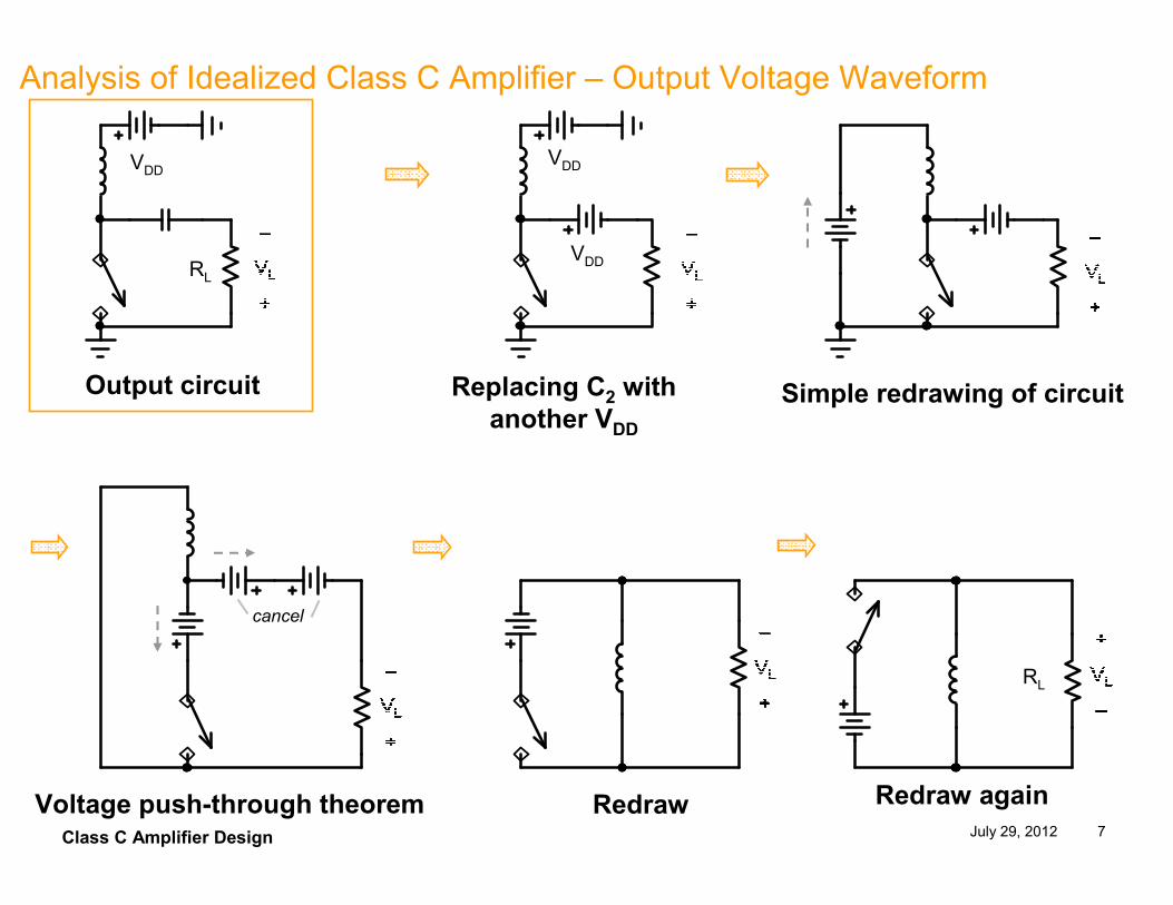
Analysis of Idealized Class C Amplifier – Output Voltage Waveform
• We seek the output voltage
waveform VL across RL
• Positive-valued input signal
closes switch
• We examine the output circuit
• For ease in finding VL, we
develop an equivalent
representation of the output
circuit
output circuit
–
VL
+
RL
Class C Amplifier Design July 29, 2012 7
Analysis of Idealized Class C Amplifier – Output Voltage Waveform
Output circuit Replacing C2 with
another VDD
Simple redrawing of circuit
Voltage push-through theorem Redraw Redraw again
cancel
VDDVDD
VDDRL
RL

Class C Amplifier Design July 29, 2012 8
Output Voltage Waveform of Idealized Class C Amplifier - 1
For t<0, input signal is at zero and switch is open
At t=0, input signal goes positive and switch closes. VL
immediately jumps to +VDD. The inductor current iLquickly but continuously rises from zero to a positive
value over 0<t<t1
At t=t1 input signal drops to zero and the switch opens
Note: The inductor current cannot change
instantaneously so iL continues to flow in the indicated
direction.
For t1<t<t2 (switch open): with a suitably large value
for L, the time constant L/R is large and iL stays
practically constant.
With iL flowing as shown after t=t1, we see that the
voltage VL has changed its polarity to negative
For t>t2 the process begins again.
signal
iL
VL
0 t1 t2 t
VDD
– VDD

Class C Amplifier Design July 29, 2012 9
Output Voltage Waveform of Idealized Class C Amplifier - 2
For t1<t<t2 (switch open):
With iL flowing as shown after t=t1, we
see that the voltage VL has changed
its polarity to negative (i.e. to −VDD)
Why is the waveform for VL
symmetric?
Because the average value (DC
value) of VL must be zero inasmuch
as VL is the voltage across an
inductor.
−iL x RL = −VDD, so iL = VDD/RL
signal
iL
VL
0 t1 t2 t
VDD
– VDD
iL = VDD/RL

Class C Amplifier Design July 29, 2012 10
Efficiency of Ideal Class C Amplifier
Efficiency = RF power out / DC power supplied
= [ VDD2 / RL ] / [ VDD x iL ]
= [ VDD2 / RL ] / [ VDD x VDD/RL ]
= 100%
Practical efficiencies realized: 50% - 80%

Class C Amplifier Design July 29, 2012 11
Simplified Class C Amplifier

Class C Amplifier Design July 29, 2012 12
Class C Amplifier Design Overview - 1
Device Selection
• Seek FETs that simulate ideal switch behavior
• Real devices have substantial input capacitance that limit switching speed
• Stability is also an issue
Input circuit
• Place “small” resistance RP across gate-source terminals
• Effective input impedance to device+shunt ≈ RP
• Input time constant now small enough so switching can occur properly at
signal frequencies
• Use impedance matching to transform source resistance (50Ω) to RP

Class C Amplifier Design July 29, 2012 13
Class C Amplifier Design Overview - 2
Output circuit
• Require additional circuitry (filtering) to cause voltage at load RL to be
sinusiodal
• Best case voltage at load is sinusoid of peak value VDD
• Power to load Pout = ½ [ VDD2 / RL ]
• Hence given power supply VDD, must adjust RL to achieve desired
output power: RL = VDD2 / (2Pout)
• Slight adjustment of formula to compensate for VDS(ON) = ID x RDS (RDS from
data sheet, estimate ID = POUT/VDD) usually negligible
• Instead, use a matching network to transform 50Ω (antenna load) to
the required value
• Additional capacitance at drain eliminates spurious oscillation

Class C Amplifier Design July 29, 2012 14
Complete Practical Class C Amplifier
input match
RP
DC
block
0.1µF
parasitic
suppression
DC
blockoutput match harmonic suppression (LPF)
50Ω
L 25µH
VDD
50Ω
antenna
not shown: RF sensor for T/R switching
50ΩRL
RL = VDD2 / (2Pout)
Select VDD=24V, Pout=50 W
RL= 5.76 Ω
Rule of thumb:
make |Xc|= 1/(ωC) ≈ 4 x RL
I used 770 pF (300+470)
|XC|=20.5Ω
Select
RP= 20 Ω
heatsink required

Class C Amplifier Design July 29, 2012 15
Input Impedance Matching
We need to transform from 50Ω to 20Ω. A ferrite transformer easily
achieves this (binocular core).
− I used type 61 ferrite; type 43 used by
others; both ok
− Selected turns ratio 8:5 (Z ratio 64:25 =
2.56:1) transforms 20Ω to ≈50Ω
− With type 61 and indicated turns, measure
10.2µH and 3.94µH for windings (647Ω
and 250Ω reactance)
− Evaluate the match on 50 Ω side by using
an antenna analyzer – seek minimum
SWR at 10.1 MHz
− Found that matching could be improved
by adding 150pF capacitor – my eventual
SWR was 1.4:1
20Ω
50Ω
for evaluation of match, connect
antenna analyzer here
8 : 5

Class C Amplifier Design July 29, 2012 16
Output Impedance Matching - 1
• Need to transform from 50Ω to 5.76Ω
• Transformer matching does not work well here because of the
relative high impedance ratio required (≈ 9:1) and the low value of
one of the terminating impedances.
• Unsuccessful attempts with both types 43 and 61 ferrite cores
• Better method here: LC impedance matching (narrowband, but
adequate for a given ham band)
• Design by (i) Smith Chart
(ii) computer-aided design tools -or-
(iii) online tools e.g.: http://leleivre.com/rf_lcmatch.html

Class C Amplifier Design July 29, 2012 17
Output Impedance Matching - 2
• Topology selection based on
experience or trial and error (only
4 variations)
• My solution: L = 246.6nH
C = 886pF
• Actual components: T80-6 core
(yellow), 5 turns (≈220nH); 820pF
silver mica capacitor
• Measured SWR < 1.2:1
50Ω from
LPF
5.76Ω
L
C
5.6Ωantenna
analyzer

Class C Amplifier Design July 29, 2012 18
Harmonic Suppression Filter standard LPF design from tables or
online tools e.g.:
http://www.calculatoredge.com/electronics/ch
%20pi%20low%20pass.htm
I used JW Miller solenoidal phenolic core inductors - from data sheet check Q, self-
resonant frequency and power handling capacity

Class C Amplifier Design July 29, 2012 19
RF Actuated T/R Switch
AMP
input
relayoutput
relay
12V (via LM7812 regulator)
820Ω
relay
5V 500Ω
10mA
to input and
output relays
0.01µF
470µF
for delay100k1000pF
0.001µF 1k
from
xmtr
to ant
2n2222a
1n4148

Class C Amplifier Design July 29, 2012 20
30m CW Amplifier – Construction - 1
6”
Complete Circuit
RF Sensor for T/R
Switching
Input Match, FET, Output
Match
Output Lowpass
Filter

Class C Amplifier Design July 29, 2012 21
30m CW Amplifier – Construction - 2
RF Sensor for T/R
Switching
Input Match, FET,
Output Match
Output Lowpass Filter

Class C Amplifier Design July 29, 2012 22
Output Spectrum Measurement
1020 40 60 80 100 140 180 MHz
down ≈40dB,
@ 60MHz
Class C Amplifier Design July 29, 2012 23
Summary and Conclusion
• Stated previous published experience for 20m
class C amplifiers
• Expanded these ideas to 30m
• Explained building-block approach to the design
• Illustrated simple evaluation of the components
• Presented construction and operation