A Predictive Resistive RAM Compact Model with Synaptic ...
4
A Predictive Resistive RAM Compact Model with Synaptic Behavior for Circuit Simulations Jia-Wei Lee, Chun-Hsiang Hsu, and Meng-Hsueh Chiang Department of Electrical Engineering, National Cheng Kung University, Tainan 701, Taiwan [email protected] ABSTRACT As one of the promising candidates of next generation memory, resistive random access memory (RRAM) does not only show good storage capability but also potential of neuromorphic operation. In this paper we introduce a compact model that could predict the bipolar switching behavior of RRAM, and the conductance of low resistance state is programmable which could mimic the synapse behavior. Design insight based on the synaptic plasticity is provided as well. Keywords: bipolar switching, compact model, resistive random access memory, RRAM, synapse 1 INTRODUCTION Artificial intelligence has come to its new era with the fast growth of machine learning algorithm. However, the conventional Von-Neumann architecture could consume excessive energy during the training process. At this moment, the memristor sheds a light on development of non-Von- Neumann architecture and provides semiconductor industry with a better solution for the optimization of certain learning algorithm[1]. Among many of the emerging memory technologies, Resistive Random Access Memory (RRAM) is regarded as one of the most promising candidates for next generation memory with its high density, fast switching speed, nonvolatile storage, low power consumption and its neuromorphic characteristic. Compared with other competitors, RRAM is more compatible with conventional CMOS fabrication environment and process[2]. Operation of RRAM with metal oxide usually contains of forming/set/reset. In the forming process, the conductive filament (CF) is generated in the dielectric layer of the Metal- Insulator-Metal structure of RRAM. Set and reset processes drive the memory to low resistant state (LRS) and high resistant state (HRS), respectively. The formation of CF could be attributed to the generation and recombination of oxygen vacancies (Vo). In order to bring the single RRAM device behavior and performance to higher system level, we provide a compact model of RRAM showing bipolar operation of programming/erase. With the physically based description of RRAM behavior, we could carry out the optimized prediction of timing and biasing in our previous work [3] that is introduced in the second part of this paper. The model is now extended to include the synaptic behavior which is introduced in the third part. 2 COMPACT MODEL The compact model is implemented for circuit simulation. With the connection of each module which is introduced in the following paragraph, this compact model is able to describe the characteristics of the bipolar switching behavior of RRAM and the model card (Table 1) is provided for the device design flexibility. Fig. 1 shows the flow of modules in this work. Forming voltage module first determines the forming voltage. Current calculation module calculates the current in LRS and accounts for the transition in reset process. Memory module switches the memory state during each process. Training module calculates the number of successive pulses (positive or negative sweep) and clears the train effect if the state changes from HRS to LRS or vice versa. Temperature module calculates the thermal effect in the RRAM cell. The model parameters could be straightforwardly calibrated and used in SPICE simulation for circuit level design. How to link the physical mechanism to the compact model is discussed next. Figure 1: Block diagram of the model. 2.1 Forming Voltage Calculation Module Forming for RRAM device is also known as soft breakdown of oxide film by electrical field. The defects cause breakdown phenomenon which could be described by the following probability equation [4]: 0 0 0 exp 1 exp 1 V Vbd S S E E P bd (1) Current calculation module Drift velocity Forming voltage calculation Memory module Temperature module Training module LRS calculation Reset process 232 TechConnect Briefs 2018, TechConnect.org, ISBN 978-0-9988782-5-6
Transcript of A Predictive Resistive RAM Compact Model with Synaptic ...
A Predictive Resistive RAM Compact Model with Synaptic Behavior for Circuit Simulations
Jia-Wei Lee, Chun-Hsiang Hsu, and Meng-Hsueh Chiang Department of Electrical Engineering, National Cheng Kung University, Tainan 701, Taiwan
ABSTRACT As one of the promising candidates of next generation
memory, resistive random access memory (RRAM) does not only show good storage capability but also potential of neuromorphic operation. In this paper we introduce a compact model that could predict the bipolar switching behavior of RRAM, and the conductance of low resistance state is programmable which could mimic the synapse behavior. Design insight based on the synaptic plasticity is provided as well.
Keywords: bipolar switching, compact model, resistive random access memory, RRAM, synapse
1 INTRODUCTION
Artificial intelligence has come to its new era with the fast growth of machine learning algorithm. However, the conventional Von-Neumann architecture could consume excessive energy during the training process. At this moment, the memristor sheds a light on development of non-Von-Neumann architecture and provides semiconductor industry with a better solution for the optimization of certain learning algorithm[1]. Among many of the emerging memory technologies, Resistive Random Access Memory (RRAM) is regarded as one of the most promising candidates for next generation memory with its high density, fast switching speed, nonvolatile storage, low power consumption and its neuromorphic characteristic. Compared with other competitors, RRAM is more compatible with conventional CMOS fabrication environment and process[2].
Operation of RRAM with metal oxide usually contains of forming/set/reset. In the forming process, the conductive filament (CF) is generated in the dielectric layer of the Metal-Insulator-Metal structure of RRAM. Set and reset processes drive the memory to low resistant state (LRS) and high resistant state (HRS), respectively. The formation of CF could be attributed to the generation and recombination of oxygen vacancies (Vo).
In order to bring the single RRAM device behavior and performance to higher system level, we provide a compact model of RRAM showing bipolar operation of programming/erase. With the physically based description of RRAM behavior, we could carry out the optimized prediction of timing and biasing in our previous work [3] that is introduced in the second part of this paper. The model is now extended to include the synaptic behavior which is introduced in the third part.
2 COMPACT MODEL
The compact model is implemented for circuit simulation.
With the connection of each module which is introduced in the following paragraph, this compact model is able to describe the characteristics of the bipolar switching behavior of RRAM and the model card (Table 1) is provided for the device design flexibility.
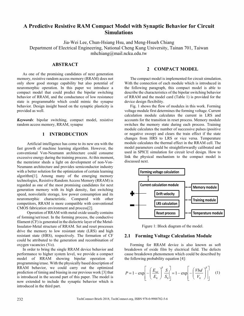
Fig. 1 shows the flow of modules in this work. Forming voltage module first determines the forming voltage. Current calculation module calculates the current in LRS and accounts for the transition in reset process. Memory module switches the memory state during each process. Training module calculates the number of successive pulses (positive or negative sweep) and clears the train effect if the state changes from HRS to LRS or vice versa. Temperature module calculates the thermal effect in the RRAM cell. The model parameters could be straightforwardly calibrated and used in SPICE simulation for circuit level design. How to link the physical mechanism to the compact model is discussed next.
Figure 1: Block diagram of the model.
2.1 Forming Voltage Calculation Module
Forming for RRAM device is also known as soft breakdown of oxide film by electrical field. The defects cause breakdown phenomenon which could be described by the following probability equation [4]:
000
exp1exp1V
Vbd
S
S
E
EP bd (1)
Current calculation module
Drift velocity
Forming voltage calculation
Memory module
Temperature module
Training moduleLRS calculation
Reset process
232 TechConnect Briefs 2018, TechConnect.org, ISBN 978-0-9988782-5-6

where Vbd is the breakdown voltage, Ebd is the breakdown electric field, S is the capacitor surface area, S0 is a reference surface area, and and E0 are the Weibull parameters.
2.2 Current Calculation Module
For drift velocity calculation, we use the equation shown below:
dx
dpqD
dx
dnqDqpqnJ pnxpxn (2)
where J is the total current density with μn (μp) mobility, Dn (Dp) diffusivity, and n (p) is the electron (hole) density.
And the motion of the ions could be described as drift current:
vqNJdrift (3)
where N is the number of ionic charge per unit volume that contributes to the drift current and v is the drift velocity [5]:
)2/sinh( TKqEaafev BTk
U
B
A
(4)
where a is the lattice constant, f is the frequency of escape attempts, UA is the activation energy, and E is the electric field. And the electron density (n) also depends on the lattice constant and electric field following
)exp(0 KT
qEann . (5)
For the LRS resistance (RLow), we apply the following equation [3]:
Limb
Low IRR 0 (6)
where R0 is the initial resistance, b is the current change parameter that affects the filament formation rate, and ILim is the current compliance. 2.3 Memory Module and Training Module
In these two modules, we use the temporary variable as a register to the current state of RRAM. In the memory module, the set_flag and reset_flag would be changed and sent to the current calculation module to desicde which of the calculation module should determine the output current. The set_flag and reset_flag could change between one and zero. In training module, each of the continuous set or reset leaves a record and acts as a factor to influence the conductance of RRAM in LRS state.
2.4 Temperature Module
The thermal dissipation (Wd ) of RRAM is given by the change of thermal energy (Q) in time [6]:
Tkt
QWd (7)
where k is the thermal conductivity and T is the temperature dispersion around the active region. The temperature in the active region (TRRAM) is evaluated with Joule heating (Wj ) and thermal dispersion (Wd ) as [6, 7]
1
0
t
t
djRRAM dt
VC
WWT (8)
where C is the heat capacity, and V is the volume of the active region in the RRAM cell. An equivalent RC model is implemented to model the temperature-dependent behaviors with
k
CVdRC RRAM (9)
where dRRAM is the thickness of the thermal dispersion media.
Parameter Description UnitT0 Temperature of environment K Rini Resistance of initial condition ΩUa Activation energy eVVthl Switching voltage of resistance state V C1 Reset-state equivalent capacitance C A Lattice constant of metal oxide cmL Length of RRAM cmVolume Heated volume in RRAM cm3
f_cr Contact area of conductive filament cm3
dr_T Heat dissipation distance of filament cm
Table 1: Main Parameters of the model card.
Figure 2: Simulated bipolar switching of an RRAM cell.
Informatics, Electronics and Microsystems: TechConnect Briefs 2018 233

3 SYNAPTIC PLASTICITY OF RRAM
The neuron cells in human brain act as message transporter by opening up the chemical channel in the synapse under arrival the electrical signal. Research works that focus on the synaptic behavior of RRAM [8, 9] show that RRAM is able to mimic the function of biological neuron. The analogy of electronic synapse and biological synapse is shown in Figure 3. The biological synapse would open its ion channel while receiving a certain electrical signal. For the RRAM case, oxygen vacancies also create an ionic channel for carriers to transport.
Figure 3: The analogy of electronic synapse and biological
synapse [8].
The HfOx-based RRAM device does not really provide the gradual set but only with gradual reset. So in order to study the synaptic behavior, we could change the current compliance of LRS to create different conductance states.
Another way to train the RRAM device is to apply a repetitively identical pulsing signal. This could also change the conductance state of RRAM [9]. By applying the above mentioned module in section 2, we could simulate how this programming technique affects the conductance change of RRAM devices, as shown in Figures 4 and 5.
Figure 4: Transient response of set operation. The LRS
current linearly changes from 1.2mA to 1.3mA with input pulses. In the module, the conductance change is set as a
linear relation with pulse number. Depending on the device characteristics, the conductance change could be linear or
non-linear.
By applying repetitive pulse treatment (training), the LRS current of the RRAM cell is improved (analogy to synapse conductance). This phenomenon may be caused by the expanded CF. Under a given bias, the chemical reaction between metal and dielectric layer creates oxygen vacancies and each of the successive pulses contributes to the formation of CF.
Figure 5: LRS current changes with repetitively identical
input pulses after 40 cycles.
4 CIRCUIT APPLICATION The application of the model in neuromorphic computing
is briefly described herein. The learning algorithm of the neural network consists of an input layer, a hidden layer and an output layer. The algorithm takes huge amount of energy and time in tuning the weights in the hidden layer in order to get the desired output.
Figure 6: Schematic of a fully connected neural network. RRAM itself is naturally suitable for accelerating the
weight (conductance) tuning in the hidden layer. And the math operation could be constructed as follows:
321
333231
232221
131211
321 III
www
www
www
vvv
. (10)
234 TechConnect Briefs 2018, TechConnect.org, ISBN 978-0-9988782-5-6

The matrix operation could be simply mapped into an RRAM crossbar (Figure 7) showing its efficiency.
Figure 7: The analogy of vector operation in the crossbar consists of RRAM cells. In each of the cross point, it
represents an RRAM device.
In our previous work, this compact model is already able to predict the RRAM array behavior [3]. The construction of the RRAM array can now be further applied to neuromorphic computing with the improved model.
5 CONCLUSION
The compact RRAM model capable of finding optimal
timing and biasing schemes has been implemented with synaptic feature based on the physical description of resistive switching behavior from drift velocity of ions in the dielectric of HRS to compliance dependent LRS. Thermal model for the temperature effect is also considered. Since RRAM is promising for larger scale arithmetic operation, this compact model provides an efficient way for circuit design and evaluation.
ACKNOWLEDGEMENT
The authors would like to thank the National Center for
High-Performance Computing, National Chip Implementation Center and National Nano Device Laboratories for technical support and the Ministry of Science and Technology of Taiwan for funding support. The neural network application was supported by Professor Darsen Lu of National Cheng Kung University.
REFERENCES
[1] T. N. Theis and H.-S. P. Wong, "The end of Moore's Law: A new beginning for information technology," Computing in Science & Engineering, vol. 19, no. 2, pp. 41-50, 2017.
[2] H.-S. P. Wong et al., "Metal–oxide RRAM," Proceedings of the IEEE, vol. 100, no. 6, pp. 1951-1970, 2012.
[3] M.-H. Chiang, K.-H. Hsu, W.-W. Ding, and B.-R. Yang, "A predictive compact model of bipolar RRAM cells for
circuit simulations," IEEE Transactions on Electron Devices, vol. 62, no. 7, pp. 2176-2183, 2015.
[4] C. Sire, S. Blonkowski, M. J. Gordon, and T. Baron, "Statistics of electrical breakdown field in Hf O 2 and Si O 2 films from millimeter to nanometer length scales," Applied Physics Letters, vol. 91, no. 24, p. 242905, 2007.
[5] D. B. Strukov and R. S. Williams, "Exponential ionic drift: fast switching and low volatility ofáthin-film memristors," Applied Physics A, vol. 94, no. 3, pp. 515-519, 2009.
[6] X. Wei et al., "HSPICE macromodel of PCRAM for binary and multilevel storage," IEEE Transactions on Electron Devices, vol. 53, no. 1, pp. 56-62, 2006.
[7] Y.-B. Liao, Y.-K. Chen, and M.-H. Chiang, "An analytical compact PCM model accounting for partial crystallization," in Electron Devices and Solid-State Circuits, 2007. EDSSC 2007. IEEE Conference on, 2007, pp. 625-628: IEEE.
[8] S. Yu, Y. Wu, R. Jeyasingh, D. Kuzum, and H.-S. P. Wong, "An electronic synapse device based on metal oxide resistive switching memory for neuromorphic computation," IEEE Transactions on Electron Devices, vol. 58, no. 8, pp. 2729-2737, 2011.
[9] J. Woo et al., "Improved synaptic behavior under identical pulses using AlO x/HfO 2 bilayer RRAM array for neuromorphic systems," IEEE Electron Device Letters, vol. 37, no. 8, pp. 994-997, 2016.
Informatics, Electronics and Microsystems: TechConnect Briefs 2018 235