
A Perspective of Frontiers in Modern Condensed Matter Physics · modern condensed matter research...
19
AAPPS Bulletin April 2008, Vol. 18, No. 2 11 A Perspective of Frontiers in Modern Condensed Matter Physics A Perspective of Frontiers in Modern Condensed Matter Physics Nai-Chang Yeh Department of Physics, California Institute of Technology, Pasadena, California 91125, USA Articles Modern condensed matter physics has evolved and expanded significantly from the scope of traditional solid state physics and has become a research field highly interdisciplinary in nature. Here we review some important recent developments that have led to conceptual and technological breakthroughs and have made significant impact on other research frontiers and applications. 1. INTRODUCTION Condensed matter physics is a branch of physics that investigates the many-body interactions and collective phenomena in the “condensed” (i.e. liquid and solid) phases of material. The scope of con- densed matter physics has evolved and expanded significantly in recent years, from traditional “solid state physics” that focuses on an effective single-particle de- scription and Landau symmetry-breaking theory for phase transitions in material, to an arena that encompasses frontiers of fundamental sciences as well as interdis- ciplinary research fields with implications on technological applications. Representa- tive examples of new scientific frontiers include: strongly correlated electronic systems, gauge theory, quantum orders and quantum phase transitions, fractional statistics and anyon models, spin liquids, and topological field theory. Regarding interdisciplinary research, some repre- sentative areas include: nano-sciences and nano-technology, spintronics, opto- electronics and organic semiconductors, nano-electronics for beyond CMOS (complementary metal oxide semicon- ductors) applications, biophysics and medical applications, laser cooled atoms and optical lattices, quantum information and computation, precise measurements and metrology, advanced materials, as- trophysics research, and energy research. The objective of this article is to provide a perspective of some of the exciting and important research frontiers in modern condensed matter physics without getting too much into the technical details, so that readers can develop better appreciation for the scope and thriving activities in this rapidly advancing and expanding research field. We shall begin with an overview of several new conceptual developments in modern condensed matter research that defy conventional wisdom, followed by reviews of representative interdisciplinary research areas that have been strongly im- pacted by the advancement in condensed matter physics. In Fig. 1 below we sum- marize the interrelations among various fields of our subsequent discussion. 2. DEFYING THE CONVENTION- AL WISDOM — NON-FERMI LIQUID BEHAVIOR & TOPO- LOGICAL ORDER In the development of modern condensed matter physics, quantum field theory (QFT) and group theory have played an essential role in the description of many-body interactions, symmetries and symmetry-breaking. The foundation of conventional condensed matter physics may be regarded as established on two conceptual cornerstones: the Fermi liquid theory, and the Landau symmetry-break- ing theory of phase transitions [1, 2]. The Fermi liquid theory treats properties of the electronic states in solids as perturbations of a ground state consisting of filling the single-particle energy levels [1, 2]. The Landau theory for phase transitions of matter classifies different phases of matter by their symmetries, so that phase transi- tions are associated with changes in the symmetry of the state of matter. However, these cornerstones no longer hold grounds when put to test against certain emerging phenomena in modern topics of condensed matter physics. For instance, various strongly correlated electronic systems such as high temperature superconductors [3-12], fractional quantum Hall (FQH) liquids in two-dimensional electron gas (2DEG) [2, 13-15], and Luttinger liquids in one-dimensional conducting systems Fig. 1: Schematic overview of fundamental physics and interdisciplinary fields in modern condensed matter research. The interrelations among different fields are indicated by the arrows.
Transcript of A Perspective of Frontiers in Modern Condensed Matter Physics · modern condensed matter research...

AAPPS Bulletin April 2008, Vol. 18, No. 2 11
A Perspective of Frontiers in Modern Condensed Matter Physics
A Perspective of Frontiers in Modern
Condensed Matter Physics
Nai-Chang Yeh
Department of Physics, California Institute of Technology,Pasadena, California 91125, USA
Articles
Modern condensed matter physics has evolved and expanded significantly from the scope of traditional solid state physics and has become a research field highly interdisciplinary in nature. Here we review some important recent developments that have led to conceptual and technological breakthroughs and have made significant impact on other research frontiers and applications.
1. INTRODUCTIONCondensed matter physics is a branch of physics that investigates the many-body interactions and collective phenomena in the “condensed” (i.e. liquid and solid) phases of material. The scope of con-densed matter physics has evolved and expanded significantly in recent years, from traditional “solid state physics” that focuses on an effective single-particle de-scription and Landau symmetry-breaking theory for phase transitions in material, to an arena that encompasses frontiers of fundamental sciences as well as interdis-ciplinary research fields with implications on technological applications. Representa-tive examples of new scientific frontiers include: strongly correlated electronic systems, gauge theory, quantum orders and quantum phase transitions, fractional statistics and anyon models, spin liquids, and topological field theory. Regarding interdisciplinary research, some repre-sentative areas include: nano-sciences and nano-technology, spintronics, opto-electronics and organic semiconductors, nano-electronics for beyond CMOS (complementary metal oxide semicon-
ductors) applications, biophysics and medical applications, laser cooled atoms and optical lattices, quantum information and computation, precise measurements and metrology, advanced materials, as-trophysics research, and energy research. The objective of this article is to provide a perspective of some of the exciting and important research frontiers in modern condensed matter physics without getting too much into the technical details, so that readers can develop better appreciation for the scope and thriving activities in this rapidly advancing and expanding research field. We shall begin with an overview of several new conceptual developments in modern condensed matter research that defy conventional wisdom, followed by reviews of representative interdisciplinary research areas that have been strongly im-
pacted by the advancement in condensed matter physics. In Fig. 1 below we sum-marize the interrelations among various fields of our subsequent discussion.
2. DEFYING THE CONVENTION-AL WISDOM — NON-FERMI LIQUID BEHAVIOR & TOPO-LOGICAL ORDER
In the development of modern condensed matter physics, quantum field theory (QFT) and group theory have played an essential role in the description of many-body interactions, symmetries and symmetry-breaking. The foundation of conventional condensed matter physics may be regarded as established on two conceptual cornerstones: the Fermi liquid theory, and the Landau symmetry-break-ing theory of phase transitions [1, 2]. The Fermi liquid theory treats properties of the electronic states in solids as perturbations of a ground state consisting of filling the single-particle energy levels [1, 2]. The Landau theory for phase transitions of matter classifies different phases of matter by their symmetries, so that phase transi-tions are associated with changes in the symmetry of the state of matter. However, these cornerstones no longer hold grounds when put to test against certain emerging phenomena in modern topics of condensed matter physics. For instance, various strongly correlated electronic systems such as high temperature superconductors [3-12], fractional quantum Hall (FQH) liquids in two-dimensional electron gas (2DEG) [2, 13-15], and Luttinger liquids in one-dimensional conducting systems
Fig. 1: Schematic overview of fundamental physics and interdisciplinary fields in modern condensed matter research. The interrelations among different fields are indicated by the arrows.

12 AAPPS Bulletin April 2008, Vol. 18, No. 2
Articles
[16-18], all involve properties that are beyond the perturbative descriptions of conventional Fermi-liquid theory. Similarly, the notion of broken symme-try associated with phase transitions are no longer applicable to the depiction of systems involving topological orders and their phase transitions. Examples include the FQH states [2, 13-15] and spin liquids [2, 3, 19, 20], where transitions among dif-ferent topological or quantum orders can occur without changing the corresponding symmetries. Hence, new conceptual foun-dations must be established to describe these emerging areas of condensed matter physics.
Throughout the history of condensed matter physics research, new materials development often breaks new grounds and leads to a new research frontier. In this section we discuss several most representative examples of new materials that have led us to a new era of condensed matter physics research that defies the con-ventional wisdom of Fermi liquid theory and Landau’s theory of broken-symmetry phase transitions. The specific examples below all belong to the so-called strongly correlated electrons, including high-tem-perature superconducting cuprates [3-12, 21], colossal magnetoresistive (CMR) manganites [22, 23], FQH states of 2DEG [13-15], electronic states of graphene [24-26], spin liquids [2, 3, 19, 20], and Luttinger liquids in one-dimensional conductors [16-18].
2.1. High-Temperature Superconduc-tivity
High-temperature superconducting cu-prates differ fundamentally from con-ventional superconductors in that they are “doped Mott insulators” [3-12]: the parent state before doping either electrons or holes into the CuO2 planes is an antifer-romagnetic insulator, with half-filling in the outer orbital and a very large on-site Coulomb repulsion that prevents double occupancy of both spin-up and spin-down electrons in the same valence states. The strong on-site Coulomb repulsion of the cuprates is in stark contrast to conven-
tional superconductors with a metallic parent state so that the kinetic energy is much larger than the Coulomb repulsion. The on-site Coulomb repulsion in the cuprates decreases with increasing dop-ing level [3, 4]. The combined effect of decreasing on-site Coulomb repulsion and increasing carrier mobility with increasing doping eventually leads to Cooper pairing and superconductivity.
There are two significant consequences due to the remnant of strong on-site Coulomb repulsion in the cuprates. One consequence is the preference for the dx2-y2-wave pairing symmetry [27-32] because it gives rise to a spatially more extended pair wavefunction relative to the s-wave pairing, so that the strong on-site Coulomb repulsion can be tactfully avoided and the overall energy of the system is lowered [3-6]. The other consequence is the oc-currence of other phases coexisting with superconductivity in the ground state [3-12]. These accompanying ordered phases are known as the competing orders [3-12], and their presence can give rise to un-conventional low-energy excitations and strong fluctuation effects that differ from the Bogoliubov quasiparticles of conven-tional superconductors [4-10]. Moreover, the physical properties at temperatures above the superconducting transition of most cuprates appear to differ significantly from the Fermi-liquid behavior of normal metals [3-10].
In principle, the occurrence of compet-ing orders as the result of strong elec-tronic correlation in the cuprates cannot be treated perturbatively, and the corre-sponding low-energy excitations are sen-sitively dependent on such parameters as the doping level, electronic anisotropy and electronic bandstructures of the system under consideration [3-9]. These problems therefore remain one of the most challeng-ing subjects in modern condensed matter physics. Empirically, different competing orders (such as antiferromagnetism [10], spin density waves [11], charge density waves [12], etc.) for different families of the cuprates have been observed, and they
may be responsible for various unconven-tional and often non-universal phenomena [4-9] that have hindered the progress of a successful microscopic theory.
Recently, new progress has been made in the phenomenology of the cuprates [5-8]. Specifically, the phenomenology incorporates competing orders and cuprate superconductivity exactly (i.e. non-pertur-batively) in the ground state with realistic physical parameters determined from experiments, and then evaluates the cor-responding low-energy quasiparticle exci-tations by allowing quantum fluctuations between coexisting phases and thermal fluctuations for temperature-induced qua-siparticle excitations. A unified descrip-tion for various seemingly non-universal behaviors has emerged [5-8]. For instance, the asymmetric phase diagrams for hole- and electron-type cuprates as illustrated in Fig. 2 as well as the accompanying physical properties (e.g. the quasiparticle spectra) can be consistently accounted for by considering the ratio of the competing order energy relative to the superconduct-ing gap and the competing order wave-vector relative to the superconducting or-der parameter [5-8]. For competing order energy larger than the superconducting gap and a competing order wave-vector parallel to the CuO2 bonding direction (which corresponds to the anti-nodal direc-tion of the dx2-y2-wave pairing potential), a “low-energy pseudogap” phase is found to arise naturally between T*(δ) and Tc(δ), which is consistent with the findings in hole-type cuprate superconductors, and many anomalous phenomena observed in this phase can be accounted for consis-tently. On the other hand, if the competing order energy is significantly smaller than the superconducting gap and if its wave-vector is parallel to the nodal direction of the dx2-y2-wave pairing potential, there is no low-energy pseudogap above Tc(δ), which is consistent with empirical findings in electron-type cuprates. Moreover, this phenomenology has provided consistent and quantitative account for quasiparticle low-energy excitation spectra determined from both angle-resolved photoemission

AAPPS Bulletin April 2008, Vol. 18, No. 2 13
A Perspective of Frontiers in Modern Condensed Matter Physics
Fig. 2: Schematic illustration of the asymmetric phase diagrams of hole-type and electron-type cuprates as a function of the doping level (δ). Here δc is a critical doping level near the optimal doping; “AFM” refers to the antiferromagnetic insulating phase, TN(δ) is the corresponding Néel temperature; “SC” denotes the superconducting phase with a transition temperature Tc(δ); “CO” represents the competing order occurring below T*(δ), which is believed to be responsible for the unconventional low-energy excitations (and therefore non-Fermi liquid behavior) occurring at Tc(δ) < T < T*(δ) of the hole-type cuprates; and TPG(δ) is associated with the onset of the high-energy pseudogap phenomena, whose energy scale is on the order of the nearest neighbor magnetic exchange energy of the Cu2+-ions in the CuO2 planes. The occurrence of different CO’s among different families of cuprates may be responsible for the asymmetric phase diagrams between hole- and electron-type and numerous non-universal properties among the cuprates.
spectroscopy (ARPES) and spatially resolved scanning tunneling microscopy/spectroscopy (STM/STS) [5-8].
Given a working phenomenology, it is natural to ask what the physical implica-tion may be in the context of microscopic pairing mechanism of cuprate supercon-ductivity. A possible route to the solution may lie in the evolution of on-site Cou-lomb repulsion with the doping level and temperature: At low temperatures a finite doping level reduces the on-site Coulomb repulsion and removes the no-double-oc-cupancy constraint in the Mott insulator limit. Hence, the nearest-neighbor antifer-romagnetic coupling favors local pairing of singlet spins (known as the Zhang-Rice singlet [33]) and the finite Coulomb repulsion prefers keeping carries apart. The local pairing of spins may lead to a doped spin-liquid state, with the resonant valence bond (RVB) states [19, 20] as possible examples. These two competing mechanisms can lead to two coexisting “channels” of interactions: one involves particle-particle or hole-hole pair interac-tions, and the other involves particle-hole scattering. Both channels are not mutually exclusive of each other as long as the on-site Coulomb repulsion is finite, and the
growth of one channel leads to the demise of the other. Thus, at low temperatures quantum tunneling of the two channels can give rise to significant quantum fluc-tuations [5-9]. Upon further increase of the carrier doping, the pairing channel expands and eventually becomes itinerant and coherent, leading to the occurrence of superconductivity. On the other hand, for non-vanishing on-site Coulomb repulsion, the particle-hole channel is still present, so that both channels correspond to coexis-tence of superconductivity and competing order. Upon increasing temperature, the low-energy excitations involve both con-tributions from the competing order and superconductivity. The presence of more than one channel of excitations can give rise to an effectively weaker superconduct-ing stiffness [5-9, 34, 35]. Moreover, the resulting quasiparticles are less coherent than those with superconductivity as the unique ground state. In the event that competing order is more dominant, as in the underdoped hole-type cuprates, superconductivity with bulk phase coher-ence will vanish first, while the remaining competing order below the pseudogap temperature T* does not entirely prohibit the occurrence of localized pairs under fluctuation effects. Consequently, the
physical properties of the pseudogap phase differ significantly from the conventional Fermi liquid behavior because there is no one-to-one correspondence between the realistic low-energy excitations and the non-interacting single-particle spectra. At this moment the verification of this scenario awaits further development in microscopic theory to rigorously account for the evolution of on-site Coulomb re-pulsion with increasing doping.
2.2. Colossal Magnetoresistive Man-ganites
Similar to the cuprate superconductors that are structurally variations of the perovskite oxides, the manganese oxides Ln1-xAxMnO3 (Ln: trivalent rare earth ions, A: divalent alkaline earth ions), also known as the manganites, are another interesting class of strongly correlated electronic systems that exhibit drastic decrease in their resis-tivity (up to six orders of magnitude) upon the application of an external magnetic field. This behavior is called the colossal magnetoresistance (CMR) [22].
The ground states of manganites are prone to be inhomogeneous because of their strong tendency to phase separate and the existence of competing orders in the ground state [22]. It is therefore not surprising that the physical proper-ties of manganites cannot be described by Fermi liquid theory. Specifically, the Mn-ions of Ln1-xAxMnO3 consist of Mn4+ and Mn3+ spin configurations; the relative ratio of Mn4+ to Mn3+ is determined by the fraction of divalent ion substitution “x”. The Mn4+ ion consists of three electrons with parallel spins in the degenerate t2g states of (3dxy, 3dyz, 3dzx), and the Mn3+ ion has an additional electron in one of the higher-energy degenerate eg states of (3dx2-y2, 3d3z2-r2). Depending on this ratio x, the ground state of the manganites can evolve from an antiferromagnetic and/or charge and orbital ordered insulator to a ferromagnetic metal [22], as exemplified in Fig. 3 for the system La1-xCaxMnO3
[36]. The strong tendency of the manga-nites to phase separate implies that the relative distribution of Mn4+ and Mn3+

14 AAPPS Bulletin April 2008, Vol. 18, No. 2
Articles
is spatially inhomogeneous for a small fraction of divalent alkaline earth ion substitution, leading to mixed domains of ferromagnetic metal and antiferromagnetic insulator. On the other hand, for 0.2 < x < 0.5, the manganites become highly conducting ferromagnetic “half metals,” with nearly 100% spin polarized majority carriers at the Fermi level [37-39]. Thus, applying an external magnetic field to the ferromagnetic manganites tends to align the ferromagnetic domains and lower the conduction carrier scattering across the domain boundaries. Furthermore, remnant antiferromagnetic insulating do-mains may be aligned by external fields, thereby giving rise to better conductance. Consequently, manganites exhibit CMR characteristics over a large chemical dop-ing range [22]. Indeed, spatially resolved scanning tunneling spectroscopic studies of the manganite La1-xCaxMnO3 below its ferromagnetic transition temperature have confirmed the aforementioned mi-croscopic picture as a function of applied magnetic field [23]. The half-metallic nature and the CMR effect associated with the manganites are in fact useful properties being explored for applications.
The sensitive interplay of the charge, spin and orbital degrees of freedom in the manganites has become a rich platform
for studying strongly correlated electrons [22]. In addition, Mn3+ is known as a Jahn-Teller ion with strong electron-phonon coupling [22]. Hence, lattice distortions also play an important role in determining the ground states and physical properties of the manganites [22].
While the manganites exhibit a rich variety of competing phases in the ground state, it is interesting to note that super-conductivity is never a possibility despite strong similarity in the physical structure and the occurrence of competing orders to the findings in the cuprates. The primary physical differences between the manga-nites and the cuprates may be the result of different spin degrees of freedom. In the manganites multiple valences with higher spin numbers are allowed energeti-cally, and the ground states are sensitively dependent on the interplay of these spin states with other charge/orbital/phonon degrees of freedom. More precisely, theo-retical studies of the manganites have re-vealed that their ground states are primar-ily determined by five contributions [22]: (1) the kinetic energy of the eg-electrons, (2) the Hund coupling energy between the eg-electron spin and the localized t2g-electron spins, (3) the antiferromagnetic coupling between the nearest-neighbor t2g-electron spins, (4) the electron-phonon coupling between the eg-electron spin and the local Jahn-Teller distortion, and (5) the Coulomb interaction among the eg-electrons. These contributions reflect the high-spin nature and the complex spin degrees of freedom. In contrast, in the cuprates the spin configuration of the copper ion is spin-1/2 and holes primar-ily reside on the oxygen site. As stated previously, the interplay of strong on-site Coulomb repulsion and nearest-neighbor antiferromagnetic coupling in the cuprates tend to energetically favor paired singlets as the spin configuration of the many-body system, no matter localized or itinerant. The paired spin singlets are effectively in the form of spin liquids, with supercon-ductivity being a special type of a doped spin liquid. Therefore, comparison of the similarities and differences between the
Fig. 3: Representative phase diagram of one of the manganites, La1-xCaxMnO3, as a func-tion of Ca substitution (x), reproduced from Ref. [36]. The notations for various phases are: FM, ferromagnetic metal; FI, ferromag-netic insulator; AF, antiferromagnetism; CO: charge/orbital ordering, PM: paramagnetism. The FI and CAF phases could be spatially inhomogeneous with coexisting FM and AF states. Moreover, it is interesting to note the singificant particle-hole asymmetry relative to x = 0.5.
manganites and cuprates seems to under-score the importance of spin pairing in cuprate superconductivity.
2.3. Fractional Quantum Hall States & Anyons
The fractional quantum Hall effect (FQHE) was first discovered in 1981 when study-ing 2DEG in a strong magnetic field [13-15]. The electronic states that demonstrate the FQH effect have been shown to contain extremely rich internal structures that are beyond Fermi liquid descriptions. These states in fact belong to a new state of mat-ter called FQH liquids [2]; different FQH states generally have different fractional charges (known as anyons) and fractional statistics, and so they belong to different quantum phases. However, these different FQH states all have the same symmetry, so that they cannot be distinguished by any explicit broken symmetry. Therefore, FQH states constitute a new type of or-der, known as the topological order. The unique properties of anyons in the FQH states have recently been recognized as po-tential candidates for the implementation of topological quantum computation [40-43], to be elaborated in a later section.
To appreciate the uniqueness of 2DEG, we note that in three and higher spatial dimensions the quantum statistics of par-ticles can be generally divided into two categories, the Fermi-Dirac (fermionic) and Bose-Einstein (bosonic) statistics with, respectively, half-integral and inte-gral spin in units of the Planck constant h. The exchange of two indistinguishable particles in these spatial dimensions can be described in terms of the permutation group. On the other hand, in the case of two spatial dimensions, particles can acquire any fractional spin and satisfy any frac-tional statistics that interpolates between the fermionic and bosonic statistics. These particles in two dimensions that obey fractional statistics are known as anyons [44], and the exchange of indistinguish-able particles in two spatial dimensions constitutes the braid group [44], with the basic operations (including the so-called Artin relations) of a braid group illustrated

AAPPS Bulletin April 2008, Vol. 18, No. 2 15
A Perspective of Frontiers in Modern Condensed Matter Physics
in Fig. 4. Specifically, if one takes an abe-lian anyon slowly around the other, (i.e. performing an adiabatic transport of one anyon around the other), the anyon will acquire a phase exp(±iθ) if 0 < θ < π. On the other hand, if θ = 0 or π (modulo 2π), then the particles are bosons or fermions, respectively. Moreover, for non-abelian anyons, the exchange of them results in non-trivial matrix representations. These anyons follow fusion and braiding rules [40, 41, 44], and can be characterized by the Chern-Simons field theory [2].
In general FQH states are classified according to the filling factor ν, which is defined as the ratio of the areal density of particles (n2D) relative to the areal density of flux quanta (B/Φ0) so that ν = n2D/(B/Φ0), where Φ0 = (h/e) is the flux quantum, B is the magnetic induction, and h and e are the Plank constant and the unit electron charge, respectively. Empirically, the fill-ing factor is associated with a measurable quantity, the Hall resistance ρxy = (h/e2)/ν. Therefore, the ρxy vs. B measurements exhibit plateaus at ν = 1, 2, 3,… known as the integer quantum Hall (IQH) states and at ν = 1/3, 2/3, 2/5, 3/5, 3/7,… known as the FQH states.
In the case of IQH effect, the 2DEG
form an incompressible state at integer fill-ing factors, and the occurrence of plateaus in ρxy is in fact associated with the presence of impurities. Given that the Hall con-ductance σxy = ν (e2/h) of the IQH state is associated with integer multiples of funda-mental constants, the IQH effect has been used as the international standard of the fundamental constant (e2/h). On the other hand, the physics of FQHE is more com-plex than the IQHE. The initial discovery of FQHE was associated with the obser-vation of Hall resistance as a function of applied B in high-mobility GaAs/AlGaAs heterostructures taking on a plateau value ρxy = 3h/e2, which corresponds to a filling factor ν = 1/3 for the lowest Landau level. For magnetic field in the plateau interval, the longitudinal resistivity ρxx also drops to zero. Consequently, the FQHE and IQHE are similar, except that the FQHE occurs primarily when the lowest Landau level is only fractionally occupied. The Coulomb repulsion in these states is very strong so that the electrons are strongly correlated. Otherwise, both the IQH and FQH states are associated with a gapped and incompressible quantum liquid. Given that the FQHE is primarily observed in the lowest Landau level, we may construct the electron state by means of a linear com-bination of the ground Landau states. For
Fig. 4: Schematic illustration of braiding group operations for anyons in (2+1) dimensions, with the vertical direction representing the world line: (a) elementary braiding operation σi of the i-th particle with the (i+1)-th particle for a system of N indistinguishable particles; (b) the elementary inverse braiding operation σi
−1; (c) the first Artin relation of a braid group σiσi+1σi = σi+1 σi σi+1 for i = 1, 2, …, (N−2); (d) the second Artin relation σiσj = σjσi for |i − j| ≤ 2; (e) An example illustrating the differences between the braid group and the permutation group.
the fractionally filled ν = m−1 state, with m being an odd integer, the wavefunction of the FQH state is:
ψm(z)=ΠNi < j (zi - zj)
mexp �Ni = 1
14 zi
2( )- ,
where the coordinate of a 2D electron is expressed as z = x + iy in units of a magnetic length lB.
The wave functions of the form in the above equation constitute the foundation for the “primitive FQH states” with m = 3, 5… However, FQHE has been observed for ν = 1/3, 2/3, 1/5, 2/5, 3/5, 2/7, 3/7, 5/7, 4/3, 7/3, 7/5, 8/5…, even at ν = 5/2. The state ν = 1 − m−1 can be considered as the electron-hole conjugate of the state m−1. For instance, the 2/3-state is conju-gate to the 1/3-state. The state ν = m−1 can be considered as the “parent state” of the fractional states ν = p/q, where q is an odd integer. For a stable ψm-state, a slight expansion of the 2DEG under a fixed magnetic field will cause a charge deficiency and cost energy. This expan-sion leads quasiholes and hierarchical FQH states with filling factor given by the following [2]:
ν = 1
m±(1/p2) ,
where p2 is a positive integer. Hence, we can obtain a hierarchy of the fractional states. For instance, for the complete filled state m = 1, if p2 = 2, we have ν = 2/3, which is the electron-hole conjugate state of ν = 1/3. For m = 3 and p2 = 2, we have ν = 2/5, 3/5, and ν = 2/7, 5/7. All these states are spin polarized. We also note that ν = 1/3 corresponds to quantum liquid with e/3 fractional charge. Equivalently, we may say that there are three flux quanta associated with each charged particle. If we no longer restrict the FQH states to the lowest Landau level, we may consider the upper spin-subband, so that ν' ≡ ν-1 , and we find the following associations of the fractional states:
4 / 3 ↔ 1 / 3, 5 / 3 ↔ 2 / 3 ↔ 1 / 3;7 / 5 ↔ 2 / 5, 8 / 5 ↔ 3 / 5 ↔ 2 / 5.
16 AAPPS Bulletin April 2008, Vol. 18, No. 2
Articles
In the case of fractional states with even denominators, such as the ν = 5/2 state [45], they are in fact spin-unpolarized states, in distinction to the ordinary spin-polarized FQH states described earlier. The ordinary spin-polarized FQH states exhibit the maximum spin polarization in high fields, and there is no mixing in Landau levels. In contrast, the FQH states with even denominators may be described as composite Fermions [46].
The FQH states, including the par-ent and the hierarchical states, can be described in terms of an effective theory known as the Chern-Simons gauge theory, which is purely topological [2]. That is, the Chern-Simons theory is only depen-dent on the topology of the manifold, not on the metric used on the manifold; any coordinate transformation involving the Chern-Simons term does not involve the Einstein metric, implying that the theory does not know about the clocks and rulers on the manifold, which is in contrast to the energy-momentum tensor that is defined by the variation of the action with respect to the Einstein metric.
The statistical properties of FQH states can be divided into abelian and non-abelian states. Specifically, non-abelian statistics means that the space of states for a collection of quasiparticles at fixed posi-tions and quantum numbers is degenerate, and when the quasiparticles are exchanged adiabatically (for which we need an energy gap for all excitations so that the non-abe-lian anyons are said to be massive), the effect is a matrix operation on this space of degenerate states. It has been pointed out that a system of non-abelian anyons with suitable properties can efficiently simulate a quantum circuit, and therefore can be applied to quantum computation [40-42]. In particular, the massive nature (or, equivalently, finite energy gaps) of these topological objects ensures robust-ness against standard environmental decoherence effects, and is therefore highly desirable for realizing quantum computation. Among the non-abelian FQH states, the states with ν = 5/2, 7/2 and 12/5
have been considered as prime candidates for employed in topological quantum computation [40-42], which opens up a new research dimension for the studies of strongly correlated electronic systems.
2.4. Luttinger LiquidMany interesting physical phenomena have been predicted for low-dimensional electronic systems. Similar to the afore-mentioned novel phenomena associated with the 2DEG, it has been established since the 1960’s and 1970’s that the electronic properties of one-dimensional conductors cannot be described perturba-tively by Fermi liquid theory [16-18]. The strong interactions in one dimension have led to incoherent motion of electrons that is better described by bosonic excitations. Moreover, the spin and charge degrees of freedom generally acquire different group velocities, leading to the so-called “spin-charge separation.” The exact solutions to this strong interaction and the resulting novel phenomena in one-dimension are
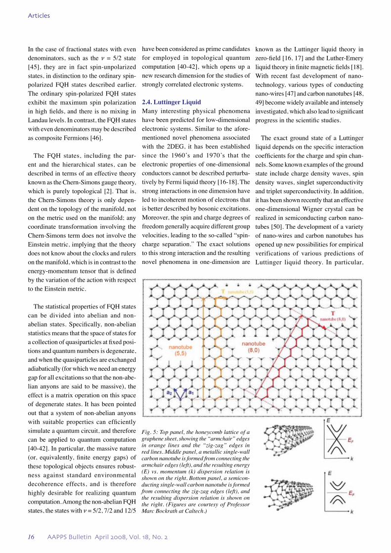
known as the Luttinger liquid theory in zero-field [16, 17] and the Luther-Emery liquid theory in finite magnetic fields [18]. With recent fast development of nano-technology, various types of conducting nano-wires [47] and carbon nanotubes [48, 49] become widely available and intensely investigated, which also lead to significant progress in the scientific studies.
The exact ground state of a Luttinger liquid depends on the specific interaction coefficients for the charge and spin chan-nels. Some known examples of the ground state include charge density waves, spin density waves, singlet superconductivity and triplet superconductivity. In addition, it has been shown recently that an effective one-dimensional Wigner crystal can be realized in semiconducting carbon nano-tubes [50]. The development of a variety of nano-wires and carbon nanotubes has opened up new possibilities for empirical verifications of various predictions of Luttinger liquid theory. In particular,
Fig. 5: Top panel, the honeycomb lattice of a graphene sheet, showing the “armchair” edges in orange lines and the “zig-zag” edges in red lines. Middle panel, a metallic single-wall carbon nanotube is formed from connecting the armchair edges (left), and the resulting energy (E) vs. momentum (k) dispersion relation is shown on the right. Bottom panel, a semicon-ducting single-wall carbon nanotube is formed from connecting the zig-zag edges (left), and the resulting dispersion relation is shown on the right. (Figures are courtesy of Professor Marc Bockrath at Caltech.)

AAPPS Bulletin April 2008, Vol. 18, No. 2 17
A Perspective of Frontiers in Modern Condensed Matter Physics
the availability of carbon nanotubes in both metallic and semiconducting forms [Fig. 5] as well as successfully developed techniques to fill the interior of these tubes with different metals [51-54] has enabled new material parameters for the studies of one-dimensional electronic systems.
2.5. GrapheneGraphene, a form of single atomic layer graphite, has quickly emerged as a promis-ing electronic material since its experimen-tal isolation in 2004 [24-26]. It consists of a single-layer, two-dimensional honey-comb lattice of carbon atoms [left panel of Fig. 6], and is a two-dimensional relative of carbon nanotubes and the buckyball C60 [24-26]. Graphene is a semi-metal, with relativistic dispersion near two Dirac points in the Brillouin zone [right panel of Fig. 6] that correspond to massless parti-cles. The isolation of graphene has ignited new research excitement in part because of its unique physical properties that promise device performance far exceeding that of silicon: (1) it has extremely high mobility (up to 15,000 cm2/Vs in as-prepared, non-optimized samples, compared to ~ 2,000 cm2/Vs for silicon); (2) its unique band structure suppresses back-scattering and enables ballistic charge transport at room temperature over hundreds of nm; (3) its thermal conductivity is expected to be comparable to that of carbon nanotubes, ~ 3,000 W/m-K [55, 56], more than 20 times improvement over silicon (150 W/m-K); (4) it has exceptional current carrying capacity, ~1010 A/cm2.
In addition to great promise in device applications, the unique properties of
graphene and the advancement of modern nano-fabrication and nano-characteriza-tion techniques promise unprecedented opportunities for researchers to investigate various novel physical properties of two- and one-dimensional electronic systems directly without undergoing complicated molecular beam epitaxial (MBE) growth of multilayer semiconductors as in the case of GaAs/AlGaAs heterostructures. Thus, graphene provides a new 2DEG system for studies of the FQH states and related anyon systems.
To date IQHE that manifests the char-acteristics of 2DEG has been observed in graphene [57], whereas observation of FQHE remains elusive. The primary dif-ficulty is likely the presence of defects and impurities incurred during the processing of graphene for measurements. With con-tinuing improvements in the material and processing techniques, research of FQH states in graphene may become realizable in the foreseeable future.
2.6. Spin LiquidsA spin liquid state is defined as an insula-tor with spin-rotation symmetry and with an odd number of electrons per unit cell. Spin liquids are novel states of matter [2] whose existence has not been proven conclusively, although recently there are new encouraging evidences for a spin liquid in the organic system of κ−(BEDT-TTF)2Cu2(CN)3 [58, 59] and generally in the spin-1/2 Heisenberg model on a Kagome lattice [60]. Theoretically, spin liquids are examples of quantum ordered states that cannot be distinguished by their symmetry properties, and the ground states of spin liquids contain topological degeneracy that cannot be related to any specific symmetry [2]. The excitations in bosonic spin liquids always carry frac-tional quantum numbers such as neutral spin-1/2, and some of these excitations also exhibit fractional statistics. Moreover, fluctuations around the ground state of spin liquids are found to consist of gauge bosons and fermions. The physical origin of the gauge fluctuations is due to the slave-boson approach [2] employed in
Fig. 6: Left Panel – Schematic diagram of the honeycomb lattice of a graphene sheet showing a sp2-bonded lattice of carbon atoms. Right Panel – Graphene band structure near one of two Dirac points. The energy-momentum dispersion relation is linear in all directions about the Dirac point.
the description of the mean-field ground state: the slave-boson description of spin liquids involves splitting a bosonic spin operator into a product of two fermionic spinon operators, which leads to a doubled Hilbert space relative to the original physi-cal system, so that gauge fluctuations are introduced to recover the original Hilbert space. This seemingly artificial manipula-tion of the bosonic spin operators (also known as the projective construction [2]) in fact can be reconciled with realistic physical observations. For instance, the physical spin wavefunction can be ex-pressed in terms of a gauge fluctuation or a pair of spinon excitations [2]. Moreover, the projective construction can lead the way to the so-called string-net-condensed state [2], a new type of correlated state with non-trivial quantum orders that are non-symmetry-breaking orders in quan-tum phases. Examples of representative and better studied spin liquids include [2]: the dimer state, RVB state, π-flux state, staggered-flux state, chiral spin state, and Z2-gapped state. Some of these spin liquid states have found interesting applications to the physical description of underdoped cuprate superconductors [3] and FQH states. Furthermore, new schemes of clas-sifying the quantum orders in spin liquids have been developed based on the concept of projective symmetry groups [2], which are analogous to the concept of symmetry groups for symmetry-breaking orders. In this context, quantum orders belonging to the same projective symmetry group exhibit the same universal properties in their ground state wavefunctions, and the universality is determined by the ansatz of the Hamiltonian.
In recent years studies of quantum spin liquids have become one of the most exciting and rapidly developing fronts in theoretical condensed matter physics. This research direction has bridged into a territory that is traditionally known as theoretical particle physics, at the same time the research has been infused with new insights from novel phenomena of condensed matter systems. It is clearly an exciting frontier for further exploration.

18 AAPPS Bulletin April 2008, Vol. 18, No. 2
Articles
3. INTERDISCIPLINARY FRON-TIERS & TECHNOLOGICAL IMPLICATIONS
In this section we touch upon some of the representative interdisciplinary research topics that are highly active in modern condensed matter physics. An overview of the interrelations of these topics can be found in Fig. 1.
3.1. Nanoscience & NanotechnologyIn December 1959, Richard P. Feynman gave a visionary speech at Caltech, entitled “There is Plenty of Room at the Bottom” [61]. This speech was unique and held a defining place in the field now known as nanoscience and nanotechnology. In approximately 7,000 words, Feynman projected a vision that is only beginning to be realized today: “What I want to talk about is the problem of manipulating and controlling things at a small scale… What I have demonstrated is that there is room – that you can decrease the size of things in a practical way. I now want to show that there is plenty of room. I will not now discuss how we are going to do it, but only what is possible in principle – in other words, what is possible according to the laws of physics.” Since the historical speech, there has been significant progress to date in this highly interdisciplinary research area now known as nanosci-ence and nanotechnology. Not only that Feynman’s vision of manipulating and controlling things down to nano- and even atomic scale becomes realizable, but novel nano-scale devices and characterization tools have also revolutionized means to exploring new science and developing new technology in a wide variety of research fields.
While steady progress towards min-iaturizing physical structures and tools has been made since Feynman’s vision-ary speech and collective efforts have reached a new pinnacle since President Bill Clinton gave his special scientific and technological strategic speech at Caltech in 1999, the strong interdisciplinary nature of nanoscience and nanotechnology is still being constant redefined and is full of both
excitement and uncertainties. Generally speaking, nanoscience and technology may be roughly divided into three subar-eas: nano-fabrication, nano-characteriza-tion, and integration of nano-structures. In what follows, we provide an overview of the status in these areas.
3.1.1. Nano-FabricationIn general the nano-fabrication techniques may be categorized into two types: the “top-down” and “bottom-up” approaches. The top-down approach is primarily based on lithographic techniques, including the traditional optical and electron-beam lithography for processing inorganic materials such as semiconductors, met-als and dielectric/ferroelectric materials. The bottom-up approach includes the nano-imprint lithography for cross-bar architecture [62], chemical lithography for self-assembled circuits [63-65], stamping techniques [66,67] for processing organic materials, multilayer soft lithography (MSL) for handling fluidic samples [68, 69], and scanning probe-based lithography (SPL) that offers novel means to manipu-late matter down to molecular and even atomic scale [70-74].
The nano-imprint lithography may in-volve the use of e-beam lithography in the processing of the mold for pattern transfer [62]. Recently nano-scale pitched layers of GaAs/GaAlAs superlattices have been employed for the mold, which enable ef-ficient fabrication of high-density metallic and semiconducting nanowires and cross-bar arrays [62]. The chemical assembly is defined as any manufacturing process whereby various electronic components (such as wires, switches and memory elements) are all chemically synthesized (i.e. “self-assembled”) and also chemically connected (i.e. “self-ordered”) to form a working circuit. Among the chemical as-sembly approaches [63], self-assembled deoxyribonucleic acid (DNA) molecules as templates have proven to be a versatile approach because they can be designed into all types of patterns [64, 65], which are promising as templates for developing large arrays of nano-scale devices, and
they may be removed subsequently after device fabrication [65]. Other naturally available nano-structures such as carbon nanotubes and graphene may also be ex-plored for bottom-up nano-fabrication.
On the other hand, for handling fluidic materials down to nano-scale, multi-layer soft lithography (MSL), a new microma-chining technique [68, 69] that exploits the elasticity and the surface chemistry of silicone elastomers to create monolithic valves within nanofluidic devices, has become a highly effective approach in nano-fabrication for handling fluidic sam-ples. Specifically, a monolithic chip can be made of multiple layers of elastomer channels, each layer having been cast from a micro-fabricated mold. In a typical two-layer system, the bottom layer consists of the fluidic channels for the introduction and manipulation of samples. The top layer has controlled channels that actuate valves pneumatically: when pressurized air or nitrogen is introduced to a controlled channel, the thin membrane between the two layers is deflected downward, which seals off the fluidic channel in the bottom layer. By further incorporating multiplex-ing, the MSL-based approach has enabled new means of handling fluidic samples on the nano-scale [69].
The traditional lithographic techniques for processing inorganic materials have been the most common approach for nano-fabrications, and are widely employed from industrial productions of silicon-based integrated circuits to prototype labo-ratory devices and novel structures (such as quantum dots [75] and single electron transistors [76]) for studying fundamental science issues such as the Kondo effect [77] and for precision measurements and metrology [78, 79]. On the other hand, the processing of organic electronics has mostly employed the soft lithography stamping technique in fabricating devices based on organic semiconductors and polymers [66, 67], because the stamp-ing approach is generally less pervasive on organic materials than conventional lithographic processing. Finally, scanning

AAPPS Bulletin April 2008, Vol. 18, No. 2 19
A Perspective of Frontiers in Modern Condensed Matter Physics
probe-based lithography (SPL) [70-74] has been applied to constructing novel nano-structures for unique scientific inves-tigations. For instance, scanning tunneling microscopy (STM) has been used to image and construct magnetic impurities directly on the surface of noble metals for the investigation of a celebrated many-body effect of magnetic spins interacting with conduction electrons, the Kondo effect [72, 73]. This new approach is in contrast to previous experimental studies that only inferred the role of the Kondo effect indi-rectly from bulk measurements of the re-sistivity and magnetic susceptibility [80]. In addition to observing how one magnetic atom such as cobalt or manganese on the surface of copper or gold may influence the surrounding electronic density of states of the host metal, how multiple magnetic atoms interacting among each other through the host metal as a function of separation have also been investigated. Moreover, artificial structures such as an elliptical “quantum corral” consisting of cobalt atoms surrounding one cobalt atom in one of the two foci of the stadium have been constructed on a copper surface by the STM technique [72, 73]. It is found that the density of states of the cobalt atom at the focal point reveals Kondo resonance. In particular, Kondo resonance is also observed at the other focal point where no cobalt atom is present. This mirror image of the Kondo resonance is referred to as a “quantum mirage” [73]. In addi-tion to STM, another popular lithography technique is the dip-pen nanolithography (DPN) [74], which is a direct-write “con-structive” lithographic tool that utilizes an “ink”-coated atomic force microscope (AFM) tip that allows both soft and hard materials to be printed from the tip onto a surface with high registration and nano-scale resolution [74]. Clearly innovative nano-structures may be devised with the capability of atomic precision in the scan-ning probe lithography.
3.1.2. Nano-CharacterizationThe invention of scanning tunneling microscopy (STM) by G. Binnig and H. Rohrer in 1981 [81] ushered a new epic
of scanning probe microscopy (SPM) that has enabled the study of local properties of materials with unprecedented spatial resolution [71]. The original STM com-bines the principle of quantum tunneling with atomic-scale piezoelectric control to achieve three-dimensional imaging capa-bilities and two-dimensional conductance spectroscopy on conducting materials with atomic resolution. To date a variety of SPM techniques have been developed for investigating other spatially resolved properties besides conductance, and they may be divided into the categories of tun-neling, force, field and hybrid microscopy [71].
The class of tunneling microscopes [71] may be considered as slight varia-tions of the STM, which include the spin-polarized STM (SP-STM) for studying spin-dependent local conductance and images of magnetic materials; ballistic electron emission microscopy (BEEM) for studying the electronic and structural properties of buried interfaces; scanning tunneling optical microscope (STOM); and scanning field emission microscope (SFEM). These tunneling microscopes in general have the best spatial resolution for both imaging and spectroscopy among all types of SPM, although they are restricted to studying conducting surfaces and are generally not suitable for insulating ma-terials. These tunneling type scanning probe microscopes have been employed at cryogenic temperatures to investigate the spatially resolved electronic properties of a wide variety of condensed matter physics systems, ranging from superconductors [31, 32], magnetic materials [23, 39], in-organic and organic semiconductors [71], to thin-film heterostructures [71].
The scanning force microscopy (SFM) is based on the response of a force sen-sor, a cantilever beam with a sharp tip at one end, to various forces. There are two types of SFM. One type is the contact force microscopy, including the atomic force microscopy (AFM) and frictional force microscopy (FFM), where the force detection is accomplished through canti-
lever deflection, which can be measured using various means such as capacitance detection, tunneling detection, laser beam deflection and optical interferometry. The other type is the non-contact force microscopy, such as the magnetic force microscopy (MFM), electrical force mi-croscopy (EFM), and van der Waal force microscopy. This type of microscopy relies on force gradient detection through ac measurements near the resonant frequency of the cantilever by modifying the effec-tive spring constant of the microscope [71]. This type of SPM generally has a spatial resolution 10 ~ 100 nm.
The field-type microscopy takes ad-vantage of the sharp probe used in SPM to achieve high spatial resolution through the near-field detection [71]. For instance, the near-field scanning optical microscope (NSOM) utilizes a sharpened optical
Fig. 7: A representative hybrid scanning probe microscope based on the combination of a cryo-genic scanning tunneling microscope (STM) and a scanning electron microscope (SEM): (a) An overview of the ultra-high vacuum STM/SEM system, including a preparation chamber, an analysis chamber, and a cryo-cooler, to-gether with a vibration isolation system. (b) A side view of the analysis chamber, showing the location of an STM head relative to the SEM electron emitter and detector and surrounded by thermal shields.

20 AAPPS Bulletin April 2008, Vol. 18, No. 2
Articles
aperture brought close (< 10 nm) to and scanned across a sample surface to detect the near-field optical signals transmitted or reflected from the sample under opti-cal illumination. In general, the near-field measurements for a probe-sample distance s <~ λ (λ being the wavelength of the probing light) provide spatial resolution better than λ/25, in contrast to the far-field (s > λ) case with resolution limited to ~ λ/2. However, the intensity of optical signals in the former decays rapidly with distance s, following the general relations of near-field intensity ∝ s−4 and far-field intensity ∝ s−2. Therefore, one of the pri-mary challenges for the field-type SPM is the signal-to-noise ratio, and to implement a servo mechanism to prevent the SPM tip from touching the sample surface.
The development of hybrid-type micros-copy aims at combining complementary techniques in one setting to achieve more versatile capabilities. A better known example is the laser-assisted STM, which employs two laser beams of powers P1 and P2 and frequencies ω1 and ω2 to il-luminate a sample under an STM tip. An ac tunneling current (Iac) of frequency Δω = (ω1 − ω2) as well as an ac voltage (Vac) are induced across the STM junc-tion. The STM response can be detected either by measuring Iac(Δω) directly or by collecting the radiation power P(Δω) ∝ [Iac(Δω)]2 [71].
Another example of a hybrid SPM being constructed by us at Caltech is a combined STM/SEM (SEM: scanning electron mi-croscope) with ultra-high vacuum (UHV) and variable temperature (VT) capabilities from ~ 4 K to room temperature, as sche-matically illustrated in Fig. 7. The ratio-nale for developing such a hybrid system is to take full advantages of both STM and SEM. Specifically, we note that while STM has the best spatial (<~ 10−2 nm) and energy (<~ 1 meV) resolutions among all of the SPM, the field of view is generally very small and the scanning rate is so slow that it is not efficient for studying isolated nano-structures in a large sample or prob-ing individual components from a large ar-
ray of nano-structures. In contrast, SEM is very effective in finding specific structures in a large sample. However, the resolution is typically limited to ~ 10 nm and there is no capability of either spectroscopy or three-dimensional imaging. By combining both STM and SEM in one UHV chamber, we can fast locate specific nano-structures of interest, perform imaging and spectro-scopic characterizations with fine spatial and energy resolution, and even utilize electron beams for in-situ annealing and structural characterization of nano-scale crystalline structures. The availability of cryogenic temperature measurements fur-ther helps improve the resolution through reduction of thermal noises, and enables the capability of studying material prop-erties as a function of temperature, which is particularly useful for investigating the evolution of electronic properties of ma-terials across phase transitions, as well as for surface science studies of such topics as surface growth, diffusion, reaction, catalysis, etc.
3.1.3. Integration of Nano-StructuresA major challenge facing the development of nanotechnology is to devise effective means to integrating a large number of nano-structures and functionalizing the collective behavior of the nanostructures with desirable properties. In recent years various types of nano-scale building blocks have been devised, including two-dimensional assembly of quantum dots with designed periodicity [82], self-assem-bly of molecular electronic circuits [83] into larger circuit elements for interfacing with macroscopic electrical contact, cross-bar architectures with demultiplexers (i.e. electronic circuits designed to separate two or more combined signals) [84], MSL processed “lab-on-a-chip” systems for sorting, transporting and analyzing fluids in small quantities [68, 69], and nano-photonic assembly towards all opti-cal processing components [85-88]. While much progress has been made, the thrust of effective integration of nano-structures remains one of the most difficult barriers to overcome for fully realizing the capacity of nanotechnology.
3.2. Spintronics for Non-Volatile Mem-ories & Logic Electronics
“Spintronics” is a new paradigm of elec-tronics based on spin-dependent properties in magnetic heterostructures [89, 90]. This field has emerged as one of the most active research areas in recent years because of its potential advantages of non-volatility, faster processing speed, and small power dissipation for high device integration densities when compared with conven-tional semiconducting devices [89, 90]. Moreover, the potential for better coher-ence in spintronics relative to typical elec-trical charge-based devices is promising for applications to quantum information technology [89-93].
To date a number of important applica-tions based on spintronics have been real-ized. For instance, in information storage, a spintronic effect known as the giant magnetoresistance (GMR) has been used in hard-drives of laptop computers [89]. Another more advanced storage technol-ogy, the magnetic random access memo-ries (MRAM) [94], can retain the memory even when the power is off and also have the switching rates and rewritability highly competitive with conventional RAM [89]. Current technology of MRAM and read heads are made of ferromagnetic metallic alloys and are based on magnetic tunnel junctions, also known as spin valves. As illustrated in Fig. 8, a magnetic tunnel junction consists of two ferromagnetic metallic layers separated by an insulator. When the two layers of ferromagnets are spin aligned, the electrical currents tunnel-ing through the barrier will exhibit a lower tunneling resistance. On the other hand, when the magnetizations of the two layers are polarized oppositely, the resulting tun-neling magnetoresistance is higher. Thus, the availability of two well defined states can be used as memory elements.
Despite proven success in information storage, further spintronic applications rely on successful incorporation of spins into semiconducting technology, which requires resolving numerous critical technical issues such as efficient injec-

AAPPS Bulletin April 2008, Vol. 18, No. 2 21
A Perspective of Frontiers in Modern Condensed Matter Physics
tion, transport, control, manipulation and detection of spin polarization. Recently progress has been made in the employ-ment of optical methods for spin injection, transport and manipulation [95]. This approach takes advantage of the ability to precisely engineer the coupling of optical photons to electron spins. In addition, developing spintronics-based qubits for quantum information technology is also being explored in spin-confined quantum-dot arrays [91-93]. While many interesting developments have been realized, progress towards a wide range of applications is still limited. In general, to address aforemen-tioned technological issues for spintronic applications requires deeper understand-ing of the fundamental science involving spin interactions with solid-state systems as a function of the electronic bandstruc-tures and dimensionality of the material involved and also with the defects in a system [89]. Therefore, the field of spin-tronics continues to be a fertile ground for scientific exploration and for promising technological advancements.
3.3. Optoelectronics for Communica-tions & Display
Optoelectronic materials and devices have provided the building blocks for rapidly developing optical communications and display technologies. Among optoelec-
Fig. 8: Schematic illustration of the operation of a spin valve based on a tri-layer magnetic tunnel junction. The tunneling junction consists of two ferromagnetic metallic layers (FM1 and FM2) separated by an insulating barrier. The tunneling magnetoresistance (TMR) depends on the relative magnetization of the two FM layers; larger TMR occurs when the magneti-zations of FM1 and FM2 are antiparallel, and smaller TMR occurs when the magnetizations of FM1 and FM2 are parallel. In realistic device applications, one of the two layers is pinned to a specific magnetization while the magnetization of the other “free” layer is controlled by an external magnetic field.
tronic materials, organic semiconductors [96, 97] are relatively new materials being intensively studied in recent years because they are highly adaptable materials with interesting optoelectronic properties that have found such applications as light emitting diodes (LED), color display, mi-cro-cavities, polymer injection lasers [96], and circuits on plastic [97]. In principle, the adaptability, weak spin-orbit interac-tion and strong polaronic properties of organic semiconductors are also suitable for incorporation into spintronics for inter-esting spin-controlled electroluminescent properties and applications [96]. Another class of optoelectronic materials is known as the photonic crystals and microphotonic materials [85]. In these photonic materials, design and engineering of the precise ge-ometry at scales comparable to the wave-length of lights have led to novel optical properties and new devices [86-88]. Some of the representative devices include opti-cally active waveguides, photonic bandgap mirrors [86, 87], micro-lasers [88], high-Q nano-cavity resonators [98], surface plas-mon-mediated light emitting diodes based on metallic nano-photonic structures [99], etc. This research field originating from conventional condensed matter physics has emerged into an important field for biological sensing and imaging. In ad-dition, with advances in lithography and pattern transfer technology, it becomes increasingly promising to overcome the major obstacle of spectral alignment and mode-matching of many optical elements on a chip and to achieve ultimate realiza-tion of nano-photonic integrated circuits. These all-optical integrated circuits on single chips can offer inexpensive wave-length division multiplexing for telecom-munications and high-speed optical data connects for data access in computing.
3.4. Nano-electronics for “Beyond CMOS” Applications
As conventional electronics follows Moore’s law to extremely high densities >~1011 devices/cm2, the traditional silicon-based complementary metal oxide semi-conductor (Si-CMOS) technology faces critical challenges such as self-heating
due to increased dissipated power density, mobility degradation, and leakage cur-rents due to charge tunneling [100]. Thus, alternative electronic materials and device integration must be sought to supplement or replace Si-CMOS technology.
There have been a number of possible beyond-CMOS technologies being ex-plored, including arrays of single-electron transistors [101], cross-bar architectures based on nano-wires [62], molecular logic devices [63, 83], and more recently spin-tronics [89, 90], DNA-templated electri-cal circuits [64, 65], and graphene-based nano-electronics [102]. To date more progress has been made in nano-wire and self-assembly approaches. In the following we focus on an interesting new paradigm, the graphene-based nano-electronics.
As mentioned in Sec. 2.5, graphene has emerged as a promising electronic mate-rial since its isolation in 2004 because of its unique material properties [24-26, 55, 56]. In addition to various highly desir-able material qualities, the geometry of graphene is planar, making it compatible with conventional lithographic techniques [102]. This characteristic resembles the properties of silicon, thus enabling multi-layer device architecture and simplifying future integration with CMOS technology. In the brief three years since its discovery, graphene already displays many properties that mimics or surpasses those of silicon, and is extremely promising as an elec-tronic material that may function as parts of active devices and interconnects.
Graphene may also have special potential in the area of information storage. Non-vol-atile solid-state memory devices comprise a multi-billion dollar market. However, the predominant platform, flash memory, expects to reach scaling limits at critical dimensions of ~ 45 nm. This limitation has strongly motivated a search for novel and non-charge based solid-state information storage that is capable of achieving sub-45 nm critical dimensions. Recent develop-ment of a novel graphene-based atomic switch [103] that likely consists of only a

22 AAPPS Bulletin April 2008, Vol. 18, No. 2
Articles
few atoms and at the same time exhibits promising device characteristics, making it capable of scaling well below the 45 nm regime. The novel switch operates by creating a nano-scale bridge of carbon atoms between two larger sheets using an electrical breakdown technique [103]. The device conductance can be changed reproducibly > 100,000 times using volt-age pulses and maintains its state for long times, making it capable of serving as a non-volatile memory element. These atomic switches can also be integrated into logic gates. Further development of the graphene atomic switches and related devices may lead to revolutionary new schemes of constructing nano-scale arrays of logic components and high-density non-volatile memories. In particular, we note that the processing of planar graphene is compatible with CMOS processing, which facilitates the integration of graphene-based devices and CMOS circuitry. Ad-ditionally, these devices can be integrated into an all-graphene electronics platform. The ultra-compact size of these devices and their potentially more superior charac-teristics make graphene-based electronics an appealing direction of exploration for beyond CMOS technology.
3.5. Laser-Cooled Systems & Optical Lattices
The development of laser techniques to trap atoms and to cool them to ultralow temperatures since 1986 [104] has ushered a new era of research that employs experi-mental techniques traditionally in atomic and molecular physics to investigate topics of many-body interactions in condensed matter physics [105-108]. A milestone in this regard was the experimental mani-festation of Bose-Einstein condensation in trapped diluted gases of alkali atoms [105-107]. Further technical developments lead to condensation of bosons consisting of Fermion pairs with varying pairing strengths tuned by a trapping magnetic field [109]. Rotating the superfluid of such Fermion pairs reveals vortices as in super-fluid helium and superconductors [109]. In addition, refined laser cooling techniques have led to the capability of trapping
atoms to either a three-dimensional [110, 111] or a two-dimensional [112] opti-cal lattice potential. This new capability enables a controlled means of simulating realistic condensed matter systems with parameters such as the lattice constant, periodic potential and particle-particle interaction strength all tunable under con-trolled optical setups. To date, in addition to observation of the Bose-Einstein con-densation in bosons and verification of the Bardeen-Cooper-Schrieffer transitions in fermions [108], a number of fundamental properties of condensed matter physics, such as the bandstructures and the two-di-mensional superfluid and one-dimensional Mott insulator have been demonstrated in the optical lattices [113]. Clearly the application of experimental techniques from atomic and molecular physics to the studies of quantum many-body physics in condensed matter has sparked much excitement and opened up new opportuni-ties for research, particularly in the area of controlled quantum dynamics that was not easily accessible in realistic condensed matter systems.
3.6. Quantum Computation & Infor-mation
The advantage of quantum computing over classical computing was first discussed by Richard Feynman in his observation that some physical phenomena could not be simulated with a classical computer [114]. Subsequently, the seminal works of Shor [115], Grover [116] and others have shown that certain types of mathematical prob-lems may be solved exponentially more efficiently by means of quantum comput-ing algorithms. Today quantum informa-tion processing has emerged as an active and rich research field because of it great promise for much improved computational speed, applications to cryptography, and for designing novel systems for studying fundamental physics issues in areas not accessible before.
Quantum computation differs from traditional computation in its extra com-putational power because it operates on information represented by quantum bits,
or qubits, rather than the classical bits of 0 and 1. A qubit can be in a superposition state that entails proportions of both 0 and 1 coexisting together, thus giving rise to unique capabilities not realizable by clas-sical bits [117].
One of the most difficult challenges in the realization of quantum computation is the dephasing time of qubits. Since the proposal of quantum computation, there has been much effort in the development of qubits. Of the many proposed technolo-gies for quantum bits (qubits), solid-state devices have perhaps the greatest potential for scalability and eventual commer-cialization because of their small sizes, straightforward fabrication methods, and robustness. A number of promising solid-state approaches are being investigated, including the superconducting Josephson junction qubits [118, 119], the spintronic qubits [91-93] based on controlling spins on quantum dots and reading out spin signals using spin polarized electrical currents, single electron transistors (SET) based on coupled low-capacitance Joseph-son junctions and quantum dots [78, 79], and topological qubits using non-abelian anyons [40-43]. Here we briefly discuss the superconducting Josephson junction qubits and theoretical concepts of the topo-logical qubits based on the FQH states.
3.6.1. Superconducting Josephson Junction Qubits for Quantum Computation
Superconducting systems are particularly attractive candidates for qubit develop-ment because of their inherently low dissi-pation, low-temperature operation (which reduces the environmental noises), and access to macroscopic quantum states [119]. Existing superconducting qubits may be classified into three types accord-ing to their relevant degrees of freedom: charge [120-122], flux [123, 124] and phase [125, 126]. Despite the scalability in the size, superconducting qubits have not acquired sufficiently long coherent times to suffice error corrections and scalable quantum computation. It is nonetheless worthwhile to introduce the underlying

AAPPS Bulletin April 2008, Vol. 18, No. 2 23
A Perspective of Frontiers in Modern Condensed Matter Physics
physical principles of operation because many innovative theoretical proposals and experimental approaches have been devised in pursuit of the ultimate prize of quantum information technology [119, 127, 128].
The simplest Josephson junction charge qubit known as a Cooper pair box is il-lustrated in Fig. 9 (a). The qubit consists of a superconducting island with n excess Cooper-pair charges connected by a tun-neling junction of capacitance CJ (typi-cally ≤ 10−15F) and a Josephson energy EJ (typically ~ 100 mK) to a superconducting electrode. A controlled gate voltage Vg is coupled to the Cooper pair box via a gate capacitor Cg. The single electron charging energy EC is determined by the total ca-pacitance of the system EC = e2/2(Cg+CJ), which is typically on the order of 1 K. When the voltage range is limited near a
degeneracy point where only two states (say n = 0 and n = 1) play a role, as shown in Fig. 9(b), while all other states are much higher in energy, the Cooper pair box becomes an effective two-state quantum system, a qubit. If we denote the charge states n = 0 and n = 1 by two effective “spin states” |↑〉 and |↓〉 respectively, it can be shown [119] that the eigenstates |0〉 and |1〉 of the qubit are given by the linear superposition of |↑〉 and |↓〉 by the following relations:
|0〉 = cos η2
|↑〉 + sin η2 |↓〉,
|1〉 = -sin η2 |↑〉 + cos η
2|↓〉,
and the mixing angle η is given by two effective magnetic fields Bx and Bz, η ≡ tan-1(Bx / Bz) , where Bx ≡ EJ and Bz ≡ 4EC(1-2ng) [119]. Hence, we observe that the eigenstates of the qubit indeed contain mixing proportions of the two states |↑〉 and |↓〉 , and the proportion of each state can be tuned by the gate charge ng.
An alternative approach to the charge degree of freedom is the manipulation of the flux degree of freedom in a Josephson flux qubit [123, 124], as schematically shown in Figs. 9(c)–(d). We shall not elaborate further about the flux qubit here, and we refer interested readers to Refs. [119, 127, 128] for further informa-tion. In practice, different variations of superconducting qubits can be devised by adding complexity to the simple de-signs illustrated in Fig. 9. For instance, architectures based on the concept of cavity quantum electrodynamics (CQED) using one-dimensional transmission line resonators coupled with Cooper pair boxes have been empirically investigated [127]. Innovative designs based on variations of Josephson junction qubits in the flux and phase degrees of freedom have also been proposed and/or studied [128]. Although the application of Josephson junction qu-bits as elements of a quantum computer remains a daunting challenge, many as-pects of quantum information processing can be readily tested on simpler quantum circuits using existing technology. It is likely that interesting spinoffs from the de-
Fig. 9: (a) A Josephson charge qubit in its simplest design, which consists of a super-conducting island with n excess Cooper-pair charges connected by a tunneling junction of capacitance CJ and a Josephson energy EJ to a superconducting electrode. A controlled gate voltage Vg is coupled to the Cooper pair box via a gate capacitor Cg. (b) The charging energy EC of the Cooper-pair box is shown as a function of the gate charge ng for different excess Cooper pairs n on the island (dashed parabolas). Near the degeneracy points, the system effectively reduces to a two-state quan-tum system because the Josephson coupling mixes with the charge states and modifies the energy of the eigenstates, as shown by the solid lines. (c) The simplest Josephson flux qubit is based on the rf-SQUID, a simple loop with a Josephson junction. (d) An improved design of a flux qubit. Here Φ denotes the flux enclosed in the rf-SQUID, and ϕ is the flux in the small loop that controls the effective Josephson coupling of the rf-SQUID [119].
velopment of quantum-state engineering can lead us to new and pleasant surprises along the way.
3.6.2. Topological Quantum Computa-tion with Non-Abelian Anyons from FQH States
Recently, proposals to explore non-abelian anyons for topological quantum computa-tion have been first suggested by A. Y. Kitaev (2003) [40] and further discussed by S. Das Sarma et al. (2005) [42] in the context of FQH states. The rationale behind applying non-abelian anyons (which are charge-flux composites) to quantum computation is primarily asso-ciated with the fact that a system of non-abelian anyons with suitable properties can simulate a quantum circuit [41], and that the “robustness” of these topological objects (i.e., the invariance of topological properties, such as the Aharonov-Bohm effect, upon smooth deformation of the system) is highly desirable for realizing effective fault-tolerance in quantum com-putation [40-43]. Specifically, the braid group irreducible representation realized by n non-abelian anyons acts on a “topo-logical vector space” Vn whose dimen-sion increases exponentially with n [41, 44]. Therefore, braiding of non-abelian anyons can simulate quantum computa-tion, because any unitary transformation acting on the exponentially large vector space Vn can be realized with arbitrarily good fidelity by choosing a suitable braid. While non-abelian anyons have great com-putational power and are fault-tolerant, it is interesting to note that abelian anyons are relevant to robust storage of quantum information because of their topological degeneracy [41].
The ability to simulate quantum circuits with non-abelian anyons rely on three capabilities of the anyon models: pair cre-ation and identification, pair annihilation, and braiding [40-42]. Physically, we may consider the general case of flux-charge composite particles in two dimensions, and non-abelian anyons may be described in terms of fluxons in two dimensions, which are flux-carrying and zero-charge

24 AAPPS Bulletin April 2008, Vol. 18, No. 2
Articles
particles. These fluxons take values in a non-abelian finite group G, which may be labeled by the group elements of G, although the labeling is not unique. That is, we may assign group elements a1, …, ak ∈ G to k fluxons, at the same time it is equally fine if we label the k fluxons by ga1g−1, …, gakg−1, where g ∈ G. However, the con-jugacy class of a set of anyons α remains invariant. In addition to fluxons, we have chargeons in two dimensions, which are charge-carrying zero-flux particles and can be labeled by the irreducible representa-tions R(α) of a group G. In general fluxons can be characterized by chargeons through the non-abelian Aharonov-Bohm effect [41]. Therefore, general particles in two di-mensions can be identified by the so-called super-selection sectors (α, R(α)). Moreover, the fusion of two particles must be left behind a localized, detectable excitation if the pair of particles has non-trivial flux/charge. Finally, we may simulate quantum gates by choosing particle world lines that realize specific particle braids. Given these capabilities, we have all the means of constructing a quantum computer from
Fig. 10: The fusion rules and braiding rules of the anyons in the FQH state ν = 5/2, also known as the Moore-Read or Pfaffian state. This state is believed to be a complex p-wave superconducting state, and its excitations can be described by the U(1) × Ising anyon model [129]. (Figures adapted from Ref. [129]).
non-abelian anyons [40-42].
As an example to appreciate the rich structures associated with non-abelian anyon models, we illustrate in Fig. 10 the fusion rules and braiding rules of the non-abelian anyons in the ν = 5/2 FQH state [129], also known as the Moore-Read or the Pfaffian state [130, 131]. This composite-fermion state is believed to be a complex p-wave superconducting state [132], and the excitations are described by the U(1) × Ising anyon model [129]. The U(1) sector consists of abelian statistics with flux/charge composites denoted by (q,Φ), whereas the Ising sector consists of non-abelian statistics with three types of particles: II (vacuum), σ (spin/vortex) and ψ (Majorana fermion). These particles obey the fusion and braiding rules illus-trated in Fig. 10. The non-trivial σ-σ fusion into ψ and the non-abelian σ-σ braiding are essential operations for their applica-tions to quantum computation.
3.7. Biophysics and MedicineOne of the best known applications of condensed matter physics to biophysi-cal and medical research is the magnetic resonant imaging (MRI) widely used in medical diagnosis [133]. The application is based on the unique sensitivity of su-perconducting devices known as SQUIDs (Superconducting QUantum Interference Devices (SQUIDs) to detect extremely small magnetic signals. The SQUIDs take advantage of a unique property of a superconductor, the macroscopic quantum phase coherence, to achieve extreme sen-sitive detection of small magnetic signals [134]. To date MRI has become an indis-pensable technology for medical diag-nostics and for biological research. While most SQUIDs are based on conventional superconductors, substantial progress has been made in SQUIDs and MRI using high temperature superconductors [133], which provides a more cost effective alternative for the technology.
An important recent trend in condensed matter physics is to exploit nanotechnolo-gy for biological and medical applications
[135]. In particular, the “lab-on-a-chip” concept associated with recent nanofluidic developments using the multilayer soft lithography (MSL) [68, 69] is promis-ing for use as miniaturized implants for future intelligent monitor, diagnosis and treatment in medicine, because these chips can simultaneously contain all necessary components on the same chip for such functions as sample handling, mixing, in-cubation, sorting, transportation, recovery, and automation. As described under Sec. 3.1, the lab-on-a-chip design typically constitutes a two-layer nanofluidic sys-tem fabricated with the MSL technique, on which pumps, valves and mixers and multiplexers are all integrated for sorting, transporting and analyzing fluids in as small quantities as pico-liters. This type of nanofluidic devices has been applied to cell sorting [68, 69, 136] and polymer-aze chain reaction (PCR) machines [137, 138]. These new advances are examples of how technical breakthroughs in nano-technology can have important impact on biological research and medicine.
3.8. Precision Measurements & Me-trology
Many experimental techniques spun off condensed matter physics research have played important roles in precision mea-surements and metrology. One of the well known examples is the integer quantum Hall effect (IQHE) that has become the conductance standard (e2/h), which is the ratio of fundamental constants, the square of the electrical charge e over the Plank constant h. Here we discuss two repre-sentative examples, the superconducting cavity-stabilized oscillator (SCSO) for frequency standard and precision mea-surements, and single electron transistors (SET) for metrology.
3.8.1. Superconducting Cavity-stabi-lized Oscillator (SCSO) for Pre-cise Frequency Measurements
The advances of clock (or, equivalently, frequency standard) technology have en-abled new opportunities for testing physics issues that require precise frequency mea-surements. Generally speaking, frequency

AAPPS Bulletin April 2008, Vol. 18, No. 2 25
A Perspective of Frontiers in Modern Condensed Matter Physics
standards can be divided into long-term and short-term oscillators, and their fre-quency stability depends on the rate of energy dissipation and changes induced by the environment. Hydrogen masers and laser-cooled cesium atomic clocks are among the best known secular long-term oscillators, whereas pulsars are Nature’s most stable clocks with unrivalled stabil-ity over years. On the other hand, super-conducting cavity-stabilized oscillators (SCSO) can provide superior frequency stabilities over short-term measurements (up to 103 ~ 104 seconds) [139].
The SCSO technology was first success-fully demonstrated in 1970’s as the best short-term clocks. Modern technological advances have opened up new prospects for further improving the frequency stabil-ity of SCSO to better than one part in 1017 ~ 1018 [139]. Specifically, optimization of SCSO technology demands several stringent technical requirements: (1) high quality-factor (Q) of the superconducting cavity to ensure a low energy dissipation rate and better frequency stability; (2) high-resolution temperature control to ensure stable temperature of the super-
conducting cavity and therefore small variations in the temperature-dependent parameters that influence the frequency stability; (3) high-resolution frequency readout and control, to lock the oscillator frequency to the resonant frequency of the superconducting cavity and to prevent fre-quency drift using the phase-locked-loop (PLL) technique; (4) advanced techniques for vibration isolation and cavity align-ment to prevent accelerations and external mechanical agitations reaching the cavity to cause frequency instability. A schematic illustration of the SCSO system is shown in Fig. 11.
While substantial progress has been made in the development of SCSO tech-niques, more rapid advances in the race for better frequency standards have been re-cently achieved in optical techniques. On the other hand, the SCSO techniques can still be applied to precision measurements of phase transitions of quantum fluids and quantum gases [139], and are also feasible for performing state-of-the-art measure-ments of fundamental constants such as the Boltzmann constant [140]. Therefore, SCSO remains a useful tool for metrology
Fig. 11: Schematic block diagram of the SCSO system at Caltech, illustrating the frequency control/readout components. The system consists of two major parts: the superconducting cav-ity-stabilized phase-locked loop (PLL) and the frequency readout component [139]. The PLL approach is to compare the cavity resonant frequency f0 with the signal output of a low-noise synthesizer at a carrier frequency fc not far from f0. By using the error voltage Verr ∝ (fc − f0) in an active feedback circuit to tune the frequency of the low-noise synthesizer, the resonant frequency f0 can be read and stabilized to high resolution (Δf/f) ~ (10-7/Q). The resolution for the frequency readout depends on the stability of the frequency standard used in the readout system. When using a second resonant mode of the same superconducting cavity as the frequency standard in the readout loop, the ultimate frequency stability on the order of 1017 ~ 1018 may be achieved [139].
and precision measurements.
3.8.2. Single Electron Transistors for Metrology
Similar to the SQUID for ultrasensitive magnetic flux measurements [133], the electrostatic “dual” of SQUID is the single electron transistor (SET), capable of ul-trasensitive charge measurements down to a fraction of a single electron charge [101]. The operation of SET electrom-eters is based on the concept of Coulomb blockade: a double-junction structure with a central metallic island is capacitively coupled (with a capacitance Cg) to an input. Under proper conditions, such a device has an onset current controlled by the potential (Vg) of the island, and the potential is periodic in the gate charge (qg = CgVg) with a periodicity equal to the charge of a single electron, e.
Since the inception [141] and first dem-onstration [142] of SET, further develop-ment of RF-SET [78] that couples the readout of the SET charge state to a reso-nant circuit and incorporates cryogenic amplifiers has improved the sensitivity and measurement speed to an extent that applications to metrology (such as electron counting current standards [143]) and sensitive measurements (such as advanced photo detectors [144]) become feasible. In addition, new physics experiments in single-electron dynamics [141, 145] and schemes of employing superconducting SET devices to generate and manipulate coherent superposition of macroscopic quantum states [119] have also been pro-posed. We expect many innovative ideas to become realizable with steady progress in the noise reduction and measurement speed improvement of the SET.
3.9. Energy Research One of the most challenging and important issues facing scientists in the 21st century is to develop clean and reusable energy, and to find effective means of storing, converting, transporting and generating energy. Here we briefly mention a recent breakthrough in fuel cell technology that is led by condensed matter research.
26 AAPPS Bulletin April 2008, Vol. 18, No. 2
Articles
Fuel cells are systems that directly and effectively convert chemical energy into electrical energy [146]. The principle of operation of fuel cells involves a cathode, an anode and an electrolyte that achieve the following overall reaction:
H2 + 12
O2 → H2O.
Of the various types of fuel cells, solid-oxide fuel cells (SOFCs) are known to yield environmentally friendly power generation and fuel flexibility [147]. However, the necessity for high operat-ing temperatures (800 °C ~ 1,000 °C) has resulted in relatively high costs and chal-lenges in finding compatible materials. As a consequence, in recent years significant efforts have been devoted to the search and development of SOFCs that may operate at lower temperatures, in the range of 500 °C ~ 700 °C. A primary obstacle to reduced-temperature operation of SOFCs is the poor activity of cathode materials for electrochemical reduction of oxygen in the lower temperature range. Specifically, the primary function of the cathode in a fuel cell based on an oxygen conducting electrolyte is to facilitate the multi-step electrochemical reduction of oxygen:
12 O2 (gas) + 2e-(cathode)
→O2-(electrolyte).
Moreover, in a single-chamber fuel cell where anode and cathode reactions take place within the same physical chamber, the cathode must be inactive towards oxidation of fuel. Therefore, operation at reduced temperatures is necessary to minimize undesirable gas phase reactions. Recently, a new cathode material based on a perovskite oxide, Ba0.5Sr0.5Co0.8Fe0.2O3−δ (BSCF), has been found to exhibit many favorable properties when incorporated into a thin-film doped ceria fuel cell with humidified hydrogen gas as the fuel and air as the cathode gas [148], including high power densities, low operating tempera-ture, and single-chamber compatibility. Further studies of the physical properties of BSCF suggest that the high power output of BSCF is the result of high rate
of oxygen diffusion through the material. The favorable characteristics of the BSCF cathode may lead to widespread practical implementation of SOFCs.
3.10. Superconducting Detectors and Mixers for Astrophysics Research
Finding answers to many important prob-lems in astronomy and cosmology rely on spectroscopic studies at millimeter through far-infrared (far-IR) frequencies, and superconducting detectors offer many benefits for research in this frequency range because of their outstanding sen-sitivity, compatibility with lithographic fabrication, and availability in large array sizes with advanced multiplexing tech-niques [149].
Generic astrophysics studies generally reply on two approaches: photometry and spectroscopy [149]. Photometry refers to measurements of a broad spectral range with relatively low spectral resolution, whereas spectroscopy refers to measure-ments of a narrower frequency spectrum with higher spectral resolution. These measurements at millimeter and sub-mil-limeter wavelengths have played a key role in the studies of early universe. Spe-cifically, photometry has been employed in studying the cosmic microwave back-ground (CMB) at millimeter wavelengths, which is the dominant electromagnetic energy of the universe and provides a snapshot of the early universe at ~ 3×10⁵ years after the Big Bang. To date measure-ments of the anisotropy of the CMB radia-tion have provided a wealth of important information, including evidence for a Euclidean universe [150-152], accurate determination of several cosmological parameters [153], and strong support for an inflation-motivated cosmological model that is dominated by dark energy and contains substantial dark matter [149]. Future measurements of the polarization of the CMB are expected to provide detailed information about the universe at the time of inflation [154]. In addition, studies of the scattering of the CMB radiation are ex-pected to help locate thousands of clusters of galaxy at all distances where they exist
[155], thereby yielding information about the history of expansion of the universe and the formation of structures in the uni-verse. A future space mission for studying these important issues associated with the CMB polarization has been planned and has called for the use of superconducting detectors [149]. Additionally, photom-etry at sub-millimeter wavelengths can measure the interstellar dust emission and provide information about the total luminosity of the galaxy, which is related to the rate of star formation [156]. While current detector technology for photom-etry at the sub-millimeter wavelengths is dominated by semiconducting bolometers [149], a new generation of bolometers based on a superconducting transition-edge sensor (TES) technology is being developed [157]. These new and improved superconducting detectors will replace semiconducting bolometers in systems under construction today.
The measurement of spectral lines also plays a critical role in astrophys-ics research. For instance, molecular rotation lines dominate at millimeter and sub-millimeter wavelengths, and atomic fine structure lines are primarily at the far-IR wavelengths. Additionally, sub-millimeter spectroscopy and interferom-etry are important for studying star and planet formation. In general, high spectral resolution (up to one part per million) is needed for detection of Doppler shifts and spectral line profiles, and also for aperture synthesis interferometry with a multiple telescope array to achieve better spatial resolution [158]. The frequency resolution can be realized by means of heterodyne re-ceivers with superconducting mixers as the frequency downconverters [158]. These mixers include superconductor-insula-tor-superconductor (SIS) tunnel junction mixers for wavelengths 3 mm > λ > 0.25 mm, and hot-electron bolometer (HEB) mixers for λ < 0.2 mm. Prior to recent developments, most heterodyne mixers are implemented using semiconductors diodes [159, 160], which generally have non-negligible noises. Recent advances in the superconducting mixer technology as

AAPPS Bulletin April 2008, Vol. 18, No. 2 27
A Perspective of Frontiers in Modern Condensed Matter Physics
well as breakthroughs in multiplexing for large arrays have offered new opportuni-ties in radio astronomy research [149], and this development is yet another example of the broad impact of modern condensed matter physics.
4. CONCLUDING REMARKSThis article provides an overview of rep-resentative aspects of modern condensed matter physics, ranging from new frontiers in fundamental physics to a wide variety of interdisciplinary research fields. From the perspective of fundamental science, we note that certain fronts of modern condensed matter physics have ven-tured into an uncharted territory beyond conventional theory; new conceptual foundations are therefore needed and are being developed. The most noteworthy topics of such research include strongly correlated electrons, spin liquids, any-ons, and topological field theory. In the interdisciplinary research fronts, many conceptual and technological spinoffs from condensed matter physics have made significant impact on other research fields and applications. Some of the most eminent examples include: nano-science and technology, spintronics, quantum computation and information, laser-cooled atoms and optical lattices, biophysics and medicine, precision measurements and metrology, energy research, and astro-physics research. Given the large scope of modern condensed matter physics, the overview described in this article cannot realistically do justice to all of the exciting activities, and are only meant to provide a glimpse into the kaleidoscopic richness of the field. What is clear to us is that the advances in condensed matter phys-ics have been constantly driven by the pursuit of fundamental physics and the unrelenting technological developments. Moreover, the strongly interdisciplinary nature of condensed matter physics will ensure its continuing intellectual vitality in the foreseeable future.
REFERENCES[1] A. A. Abrikosov, L. P. Gorkov, and
I. E. Dzyaloshinski, in Methods of Quantum Field Theory in Statisti-cal Physics.
[2] X.-G. Wen, in Quantum Field The-ory of Many-Body Systems (Oxford University Press, 2004).
[3] P. A. Lee, N. Nagaosa, and X.-G. Wen, Rev. Mod. Phys. 78, 17 (2006).
[4] N.-C. Yeh, Highlight, Bulletin of Association of Asia Pacific Physi-cal Societies (AAPPS), Vol. 12, No. 2, pp. 2-20 (2002). [cond-mat/0210656]
[5] N.-C. Yeh et al., Int. J. Mod. Phys. B 19, 285 (2005).
[6] N.-C. Yeh, C.-T. Chen, A. D. Beyer, and S. I. Lee, Chinese J. of Phys. 45, 263 (2007).
[7] C.-T. Chen, A. D. Beyer, and N.-C. Yeh, Solid State Commun. 143, Fast Communications, 447 (2007).
[8] A. D. Beyer, C.-T. Chen, and N.-C. Yeh, to Physica C 468, 471 (2008).
[9] A. D. Beyer et al., Phys. Rev. B 76, 140506(R) (2007).
[10] S.-C. Zhang, Science 275, 1089 (1997); S.-C. Zhang et al., Phys. Rev. B 60, 13070 (1999).
[11] E. Demler and S.-C. Zhang, Phys. Rev. Lett. 75, 4126 (1995); E. Dem-ler, S. Sachdev, and Y. Zhang, Phys. Rev. Lett. 87, 067202 (2001).
[12] S. A. Kivelson et al., Rev. Mod. Phys. 75, 1201 (2003).
[13] D. C. Tsui, H. L. Stormer, and A. C. Gossard, Phys. Rev. Lett. 48, 1559 (1982).
[14] R. B. Laughlin, Phys. Rev. B 23, 5632 (1981).
[15] B. I. Halperin, Phys. Rev. B 25, 2185 (1982).
[16] S. Tomonoga, Prog. Theor. Phys. 5, 544 (1950).
[17] J. M. Luttinger, J. Math. Phys. 4, 1154 (1963).
[18] A. Luther and V. J. Emery, Phys. Rev. Lett. 33, 589 (1974).
[19] P. W. Anderson, Science 235, 1196 (1987); Science 279, 1196 (1998).
[20] G. Kotliar, Phys. Rev. B 37, 3664 (1988).
[21] J. G. Bednorz and K. A. Muller, Z. Phys. B64, 189 (1986).
[22] E. Dagotto, T. Hotta, and A. Moreo, Phys. Rep. 344, 1 (2001).
[23] M. Fath et al., Science 285, 1540 (1999).
[24] K. S. Novoselov et al., Nature 438, 197 (2005).
[25] K. S. Novoselov et al., Science 306, 666 (2004).
[26] Y. Zhang, Y. W. Tan, H. L. Storm-er, and P. Kim, Nature 438, 201 (2005).
[27] D. Pines, Physica C 235, 113 (1994).
[28] D. Scalapino, Phys. Rep. 250, 329 (1995).
[29] D. J. Van Harlingen, Rev. Mod. Phys. 67, 515 (1995).
[30] C. C. Tsuei and J. R. Kirtley, Rev. Mod. Phys. 72, 969 (2000).
[31] N.-C. Yeh et al., Phys. Rev. Lett. 87, 087003 (2001); Physica C 364-365, 450 (2001).
[32] J. Y. T. Wei et al., Phys. Rev. Lett. 81, 2542 (1998).
[33] F. C. Zhang and T. M. Rice, Phys. Rev. B 37, 3759 (1988).
[34] V. J. Emery and S. A. Kivelson, Nature 374, 434 (1995).
[35] Y. J. Uemura, G. M. Luke, and B. J. Sternleib et al., Phys. Rev. Lett. 62, 2317 (1989).
[36] S.-W. Cheong and H. Y. Hwang, in Contributions to Colossal Magne-toresistance Oxides, Monographs in Condensed Matter Science, ed. by Y. Tokura (Gordon and Breach, London, 1999).
[37] W. E. Pickett and D. J. Singh, Phys. Rev. B 53, 1146 (1996).
[38] N.-C. Yeh et al., J. Phys. Condens. Matter 9, 3713 (1997); J. Appl. Phys. 81, 5499 (1997).
[39] J. Y. T. Wei, N.-C. Yeh, and R. P. Vasquez, Phys. Rev. Lett. 79, 5150 (1997).
[40] A. Y. Kitaev, Ann. Phys. 303, 2 (2003).
[41] J. Preskill, “Topological quantum

28 AAPPS Bulletin April 2008, Vol. 18, No. 2
Articles
computations,” Caltech lecture notes (2004).
[42] S. Das Sarma, M. Freedman, and C. Nayak, Phys. Rev. Lett. 94, 166802 (2005).
[43] G. P. Collins, Scientific America 294, 57 (2006).
[44] A. Khare, Fractional Statistics and Quantum Theory (World Scientific, 2005), 2nd edition.
[45] R. Willett et al., Phys. Rev. Lett. 59, 1776 (1987).
[46] J. K. Jain, Phys. Rev. B 40, 8079 (1989).
[47] C. N. Lau et al., Phys. Rev. Lett. 87, 217003 (2001).
[48] M. Bockrath et al., Science 291, 283 (2001).
[49] H.-Y. Chiu et al., Phys. Rev. Lett. 95, 226101 (2005).
[50] M. Bockrath, private communica-tions.
[51] A. Leonhardt et al., Diamond and related materials 12, 790-793 (2003).
[52] Y. K. Chen et al., J. Mat. Chem. 7, 545-549 (1997).
[53] M. Monthioux, Carbon 40, 1809-1823 (2002).
[54] C. H. Liang et al., J. Crystal Growth 218, 136-139 (2000).
[55] P. Kim, L. Shi, A. Majumdar, and P. L. McEuen, Phys. Rev. Lett. 87, 215502 (2001).
[56] C. H. Yu et al., Nano Lett. 5, 1842 (2005).
[57] C.-N. Lau, private communica-tions.
[58] S.-S. Lee and P. A. Lee, Phys. Rev. Lett. 95, 036403 (2005).
[59] S.-S. Lee, P. A. Lee, and T. Sent-hil, Phys. Rev. Lett. 98, 067006 (2007).
[60] Y. Ran, M. Hermele, P. A. Lee, and X.-G. Wen, Phys. Rev. Lett. 98, 117205 (2007).
[61] R. P. Feynman’s lecture may be seen at the URL http://www.its.caltech.edu/~feynman/.
[62] G. Y. Jung et al., Nano Lett. 6, 351 (2006).
[63] M. C. Petty, M. R. Bryce, and D.
Bloor, eds. for Introduction to Molecular Electronics (Edward Arnold, London, 1995).
[64] P. W. K. Rothemund, Nature 440, 297-302 (2006).
[65] R. D. Barish, P. W. K. Rothemund, and E. Winfree, Nano Lett. 5, 2586-2592 (2005).
[66] B. D. Gates et al., Chem. Rev. 105, 1171 (2005).
[67] Y.-L. Loo, D. V. Lang, J. A. Rog-ers, and J. W. P. Hsu, Nano. Lett. 3, 913 (2003).
[68] M. A. Unger et al., Science 288, 113 (2000).
[69] S. R. Quake and A. Scherer, Science 290, 1536 (2000).
[70] D. M. Eigler and E. K. Schweizer, Nature 344, 524 (1990).
[71] For a comprehensible review of the operation principle, varieties, as well as applications of SPM, see, for example, R. Weisendanger, Scanning Probe Microscopy and Spectroscopy – Methods and Ap-plications (Cambridge University Press, 1994).
[72] M. F. Crommie, C. P. Lutz, and D. M. Eigler, Science 262, 218 (1993).
[73] H. C. Manoharan, C. P. Lutz, and D. M. Eigler, Nature 403, 512 (2000).
[74] K. Salaita, Y. Wang, and C. A. Mirkin, Nature Nanotech. 2, 145 (2007).
[75] L. P. Kouwenhoven and C. M. Marcus, Physics World, June, pp. 35-39 (1998).
[76] D. Goldhaber-Gordon et al., Nature 391, 156 (1998).
[77] L. P. Kouwenhoven and L. Glazman: Physics World, January, pp. 33-38 (2001).
[78] R. J. Schoelkopf et al., Science 280, 1238 (1998).
[79] A. Shnirman and G. Schön, Phys. Rev. B 57, 15400 (1998).
[80] J. Kondo, Prog. Theor. Phys. 32, 37 (1964).
[81] G. Binnig and H. Rohrer, Rev. Mod. Phys. 59, 615 (1987).
[82] R. H. Chen, A. N. Korotov, and K. K. Likharev, Appl. Phys. Lett. 68, 1954 (1996).
[83] C. P. Collier et al., Science 285, 391 (1999).
[84] R. Beckman et al., Science 310, 465 (2005).
[85] E. Yablonovitch and T. J. Gmitter, Phys. Rev. Lett. 63, 1950 (1989).
[86] J. S. Foresi et al., Nature 390, 143 (1997).
[87] O. Painter et al., Science 284, 1819 (1999).
[88] U. Mohideen et al., Appl. Phys. Lett. 64, 1911 (1994).
[89] S. A. Wolf et al., Science 294, 1488 (2001).
[90] D. D. Awschalom, M. E. Flatté, and N. Samarth, Sci. Am. June, pp. 67-73 (2002).
[91] R. K. Kawakami et al., Science 294, 131 (2001).
[92] D. Loss and D. P. DiVincenzo, Phys. Rev. A 57, 120 (1998).
[93] H.-A. Engel and D. Loss, Phys. Rev. Lett. 86, 4648 (2001).
[94] A. Cho, Science 296, 246 (2002).[95] J. A. Gupta, R. Knobel, N. N. Sam-
arth, and D. D. Awschalom, Science 292, 2458 (2001).
[96] R. H. Friend et al., Nature 397, 121 (1999).
[97] S. Forrest, P. Burrows, and M. Thompson, IEEE Spectrum, August , pp. 29-34 (2000).
[98] T. Baehr-Jones, M. Hochberg, C. Walker, and A. Scherer, Appl. Phys. Lett. 85, 3346 (2004).
[99] K. Okamoto et al., Nature Materials 3, 601 (2004).
[100] R. R. Schaller, IEEE Spectrum 34, 53 (1997).
[101] D. V. Averin and K. K. Likharev, in Microscopic Phenomena in Solids, ed. B. Altshuler, P. Lee, and R. Webb (Elsevier Amsterdam, 1991), p. 173.
[102] C. Berger et al., Science 312, 1191 (2006).
[103] M. Bockrath, private communica-tions (2008).
[104] S. Chu and C. Cohen-Tannoudji,

AAPPS Bulletin April 2008, Vol. 18, No. 2 29
A Perspective of Frontiers in Modern Condensed Matter Physics
and W. D. Phillips, Rev. Mod. Phys. 70, 685 (1998).
[105] M. H. Anderson et al., Science 269, 198 (1995).
[106] K. B. Davis et al., Phys. Rev. Lett. 75, 3969 (1995).
[107] C. C. Bradly et al., Phys. Rev. Lett. 75, 1687 (1995); Phys. Rev. Lett. 78, 985 (1997).
[108] C. J. Pethick and H. Smith, Bose-Einstein Condensation in Dilute Gases (Cambridge University Press, 2002).
[109] M. W. Zwierlein et al., Nature 435, 1047 (2005).
[110] A. Kastberg et al., Phys. Rev. Lett. 74, 1542 (1995).
[111] M. Gatzke et al., Phys. Rev. A 55, R3987 (1997).
[112] S. E. Hamann et al., Phys. Rev. Lett. 80, 4149 (1998).
[113] S. Bergkvist et al., Phys. Rev. Lett. 99, 110401 (2007).
[114] R. P. Feynman, “Simulating physics with computers,” Int. J. of Theor. Phys. 21, 467 (1982).
[115] P. W. Shor, SIAM J. Sci. Statist. Comput. 26, 1484 (1997).
[116] L. K. Grover, Proc. 28th Annual ACM Symp. on the Theory of Com-puting, 212 (1996).
[117] M. A. Nielsen, “Rules for a com-plex quantum world,” Sci. Am. November (2002).
[118] M. H. Devoret and J. M. Martinis, Quantum Information Processing 3, 163 (2004).
[119] Y. Makhlin, G. Schön, and A. Shnirman, Rev. Mod. Phys. 73, 357 (2001).
[120] V. Bouchiat et al., Phys. Scr. T76, 165 (1998).
[121] Y. Nakamura, C. D. Chen, and J. S. Tsai, Phys. Rev. Lett. 79, 2328 (1997).
[122] Y. Nakamura, Y. A. Paskin, and J. S. Tsai, Nature 398, 786 (1999).
[123] J. E. Mooij et al., Science 285, 1036 (1999).
[124] J. R. Friedman et al., Nature (Lon-don) 406, 43 (2000).
[125] J. M. Martinis, S. Nam, J. Aumen-tado, and C. Urbina, Phys. Rev. Lett. 89, 117901 (2002).
[126] K. B. Cooper et al., Phys. Rev. Lett. 93, 180401 (2004).
[127] A. Blais et al., Phys. Rev. A 69, 062320 (2004).
[128] J. Koch et al., Phys. Rev. A 76, 042319 (2007).
[129] P. Bonderson, A. Kitaev, and K. Shtengel, Phys. Rev. Lett. 96, 016803 (2006).
[130] G. Moore and N. Read, Nucl. Phys. B 360, 362 (1991).
[131] C. Nayak and F. Wilczek, Nucl. Phys. B 479, 529 (1996).
[132] N. Read and D. Green, Phys. Rev. B 61, 10267 (2000).
[133] J. Clarke, Scientific American 271 (2), 46 (1994); Proc. IEEE 77, 1208 (1989).
[134] M. Tinkham, Introduction to Super-conductivity (McGraw-Hill, New York, 1996), 2nd edition.
[135] M. L. Roukes, Sci. Am. 285, 48 (2001)
[136] P. H. Li and D. J. Harrison, Anal. Chem. 69, 1564 (1997).
[137] L. C. Waters, Anal. Chem. 70, 158 (1998).
[138] M. U. Kopp, A. J. de Mello, and A. Manz, Science 280, 1046 (1998).
[139] T. A. Corcovilos, D. M. Strayer, N. Asplund, and N.-C. Yeh, J. of Low Temp. Phys. 134, 431 (2004); N.-C. Yeh, D. M. Strayer, V. L. Anderson, and N. Asplund, Physica B 280, 557 (2000).
[140] T. A. Corcovilos, Ph.D. thesis, Caltech (2007).
[141] D. V. Averin and K. K. Likharev, J. Low Temp. Phys. 62, 345 (1986).
[142] T. A. Fulton and G. J. Dolan, Phys. Rev. Lett. 59, 109 (1987).
[143] K. K. Likharev, in Granular Elec-tronics, NATO ASI Series B: Phys-ics, ed. D. Ferry (Plenum, New York, 1990), Vol. 251.
[144] A. N. Cleland, D. Esteve, C. Ur-bina, M. H. Devoret, Appl. Phys. Lett. 61, 2820 (1992).
[145] K. K. Likharev and A. B. Zorin, J. of Low Temp. Phys. 59, 347 (1985).
[146] B. C. H. Steele and A. Heinzel, Nature 414, 345 (2001).
[147] N. P. Brandon, S. Skinner, and B. C. H. Steele, Annu. Rev. Mater. Res. 33, 183 (2003).
[148] Z. Shao and S. M. Haile, Nature 431, 170 (2004).
[149] J. Zmuidzinas and P. L. Richards, Proc. IEEE 92, 1597 (2004).
[150] P. de Bernardis et al., Nature 404, 955 (2000).
[151] S. Hanany et al., Astrophys. J. 545, L5 (2000).
[152] N. Halverson et al., Astrophys. J. 568, 38 (2002).
[153] S. Spergel et al., Astrophys. J. (Suppl.) 148, 175 (2003).
[154] M. Kamionkowski and A. Ko-sowsky, and A. Stebbins, Phys. Rev. Lett. 78, 2058 (1997); Phys. Rev. D 57, 685 (1998).
[155] J. E. Carlstrom, G. P. Holder, and E. D. Reeze, Annu. Rev. Astron. Astrophys. 40, 643 (2002).
[156] P. M. Harvey et al., Proc. SPIE, IR Space Telescope Instrum. Vol. 4850, 1097 (2003).
[157] P. L. Richards, Proc. Far-IR Sub-MM and MM Detector Workshop, NASA/P-2003-211408, eds. J. Wolf, J. Farhoomand, and C. R. McCreight (2003), p. 219.
[158] J. Zmuidzinas, Proc. Far-IR Sub-MM and MM Detector Workshop, NASA/P-2003-211408, eds. J. Wolf, J. Farhoomand, and C. R. McCreight (2003), p. 149.
[159] T. Phillips and D. Woody, Annu. Rev. Astron. Astrophys. 20, 285 (1982).
[160] J. Archer, Proc. IEEE 73, 109 (1985).


![Phase Transitions in Condensed Matter Hans … · 2 References [1] Stephen Blundell, Magnetism in Condensed Matter, Oxford University Press [2] Igot Herbut, A Modern Approach to Critical](https://static.fdocuments.net/doc/165x107/5b5db4e47f8b9a16498ea383/phase-transitions-in-condensed-matter-hans-2-references-1-stephen-blundell.jpg)


