A Novel Self-Powered Dynamic System Using a Quasi-Z-Source ...
21
Electronics 2020, 9, 265; doi:10.3390/electronics9020265 www.mdpi.com/journal/electronics Article A Novel Self-Powered Dynamic System Using a Quasi-Z-Source Inverter-Based Piezoelectric Vibration Energy Harvester Wesley Qi Tong Poh *, Muhammad Ramadan Bin Mohamad Saifuddin and Ramasamy Thaiyal Naayagi School of Electrical and Electronics, Newcastle University in Singapore, Newcastle Research and Innovation Institute, Singapore 609607, Singapore; [email protected] (M.R.B.M.S.); [email protected] (R.T.N.) * Correspondence: [email protected] Received: 27 December 2019; Accepted: 3 February 2020; Published: 5 February 2020 Abstract: The use of quasi-Z-source inverters (qZSIs) for DC-DC power conversion applications has gained much recognition when dealing with grid-tied renewable energy resource integrations. This paper proposes a novel self-powered dynamic system (SPDS) involving a piezoelectric vibration energy harvester (PVEH) using qZSI to establish interoperability with a DC load rated at 16.15 mW. Based on uncertain output performances from a piezoelectric cantilever beam (CB), the qZSI-based PVEH serves as a dynamic voltage restoration unit that establishes load-following synchronisation. It uses a proportional-integral based boost controller (PI-based BC) to generate strategic ordering of shoot-through voltage amplification into pulse-width modulation (PWM) gating sequences. The SPDS was modelled using two software based on commercially available product specifications: (i) COMSOL Multiphysics to mechanically design and optimise a CB. (ii) PSCAD/EMTDC to electronically design and integrate the qZSI with the optimised CB, while functioning as a testbed to model the SPDS against arbitrary wind speed and structural vibration frequency data collected from an above-ground mass rapid transit (MRT) train station in Khatib, Singapore. The acquired simulation results have depicted desirable transient responses at respective sub-systems, procuring fast settling-time responses, negligible steady-state error, as well as high efficiencies of 94.07% and 91.64% for the CB and SPDS respectively. Keywords: energy harvesting; self-powered dynamic system; piezoelectric device; DC-DC power converter; voltage-controlled oscillator; integrated circuit modelling 1. Introduction Research efforts on self-powered dynamic systems (SPDSs) involving vibration-based energy harvesting have gained interest due to the relevancy of their deployment to sustainable urban energy planning. They can replicate operational benefits similar to either solar or wind energy harvesting systems that possess compact circuitry design and lower installation costs, whilst achieving greater sensitivity towards environment variations [1–3]. Vibration-based energy harvesting technology is commonly associated with piezoelectric mechanisms that convert mechanical energy into electrical energy based on detected ambient vibrations. Notably, the piezoelectric vibration energy harvester (PVEH) is known for its high power density and high energy conversion efficiency [4–7]. The PVEH typically employs a piezoelectric cantilever beam (CB) with a proof mass mounted at its free end while its other end is fixed to a centralised, vibrating host structure. Whenever ambient vibrations are propagated across the host structure, the CB’s free end resonates in vertical oscillatory motion to
Transcript of A Novel Self-Powered Dynamic System Using a Quasi-Z-Source ...

Electronics 2020, 9, 265; doi:10.3390/electronics9020265 www.mdpi.com/journal/electronics
Article
A Novel Self-Powered Dynamic System Using a Quasi-Z-Source Inverter-Based Piezoelectric Vibration Energy Harvester Wesley Qi Tong Poh *, Muhammad Ramadan Bin Mohamad Saifuddin and Ramasamy Thaiyal Naayagi
School of Electrical and Electronics, Newcastle University in Singapore, Newcastle Research and Innovation Institute, Singapore 609607, Singapore; [email protected] (M.R.B.M.S.); [email protected] (R.T.N.) * Correspondence: [email protected]
Received: 27 December 2019; Accepted: 3 February 2020; Published: 5 February 2020
Abstract: The use of quasi-Z-source inverters (qZSIs) for DC-DC power conversion applications has gained much recognition when dealing with grid-tied renewable energy resource integrations. This paper proposes a novel self-powered dynamic system (SPDS) involving a piezoelectric vibration energy harvester (PVEH) using qZSI to establish interoperability with a DC load rated at 16.15 mW. Based on uncertain output performances from a piezoelectric cantilever beam (CB), the qZSI-based PVEH serves as a dynamic voltage restoration unit that establishes load-following synchronisation. It uses a proportional-integral based boost controller (PI-based BC) to generate strategic ordering of shoot-through voltage amplification into pulse-width modulation (PWM) gating sequences. The SPDS was modelled using two software based on commercially available product specifications: (i) COMSOL Multiphysics to mechanically design and optimise a CB. (ii) PSCAD/EMTDC to electronically design and integrate the qZSI with the optimised CB, while functioning as a testbed to model the SPDS against arbitrary wind speed and structural vibration frequency data collected from an above-ground mass rapid transit (MRT) train station in Khatib, Singapore. The acquired simulation results have depicted desirable transient responses at respective sub-systems, procuring fast settling-time responses, negligible steady-state error, as well as high efficiencies of 94.07% and 91.64% for the CB and SPDS respectively.
Keywords: energy harvesting; self-powered dynamic system; piezoelectric device; DC-DC power converter; voltage-controlled oscillator; integrated circuit modelling
1. Introduction
Research efforts on self-powered dynamic systems (SPDSs) involving vibration-based energy harvesting have gained interest due to the relevancy of their deployment to sustainable urban energy planning. They can replicate operational benefits similar to either solar or wind energy harvesting systems that possess compact circuitry design and lower installation costs, whilst achieving greater sensitivity towards environment variations [1–3]. Vibration-based energy harvesting technology is commonly associated with piezoelectric mechanisms that convert mechanical energy into electrical energy based on detected ambient vibrations. Notably, the piezoelectric vibration energy harvester (PVEH) is known for its high power density and high energy conversion efficiency [4–7]. The PVEH typically employs a piezoelectric cantilever beam (CB) with a proof mass mounted at its free end while its other end is fixed to a centralised, vibrating host structure. Whenever ambient vibrations are propagated across the host structure, the CB’s free end resonates in vertical oscillatory motion to

Electronics 2020, 9, 265 2 of 21
generate electrical power. The proof mass expedites this power generation process by reducing the CB’s resonant frequency to match the ambient vibration frequency [8].
1.1. Cantilever Beam Configurations
Different CB configurations were explored for optimised energy harvesting. Abasian et al. [9] proposed a CB that features a miniature permanent magnet (PM) at the tip of its free end instead of a non-magnetic proof mass. However, this design is only compatible with AC-based systems as the interaction between PM and the magnetic field will induce vibrations across the CB to generate power. Moreover, it was discovered that the narrow operational bandwidth of CBs is generally difficult to overcome using magnetic-based configurations, as the PM only operates optimally at a specific angle for all magnetisation vectors. To overcome this limitation, unimorph-configured CB that was designed with a single piezoelectric layer made of lead zirconate titanate (PZT), fused with an elastic charge conductor layer made of silicon, as well as a proof mass is proposed in [10]. Experimental results proved that by incrementing the dimensions of both layers and volume of the proof mass proportionally, the CB’s resonant frequency will be greatly reduced to match the ambient vibration frequency. Subsequently, [11] suggested a superior unimorph-configured CB concept by proposing an additional PZT layer to form a composite beam known as the bimorph. It improves the tunable effectiveness of the proof mass, since doubled output peak power is observed when compared to the unimorph. Power was transferred to the load with improved electromechanical coupling and impedance matching.
1.2. Power Management Frameworks
Various research works have been initiated into engineering-suitable power conversion systems that can harvest optimal power generation from PVEH technology [12–15]. Typically, it involves a centralised isolated or non-isolated DC-DC converter to perform either buck or boost operations before transferring power to the load. Two major challenges arise whenever conventional DC-DC converters are operated in conjunction with the CB; (i) the piezoelectric material exhibits large capacitance, and a primitive approach requires an impractical-sized inductor on the load, (ii) the CB’s impedance varies according to the environmental condition. Hence, impedance matching methods such as conjugate matching [16] and resistive matching [17] are proposed. Conjugate matching uses switching devices (e.g., insulated-gate bipolar transistors, or IGBTs) and inductors for shaping the output voltage and current waveforms to alter the load impedance, thus enabling a higher power transfer for a wider vibration frequency range as compared to resistive matching. Since the switching devices should be switched synchronously with the displacement of the beam, it is inherently difficult to conform to rigorous timing control with simple circuitry and low power consumption [18,19]. However, resistive matching can only be realised if the impedance of the CB vibrating around the resonant frequency is mostly resistive [17–20]. Existing power management circuits that employ impedance matching methods have not addressed practical concerns such as synchronous switching enablement and efficient power transfer in SPDSs.
In order to alleviate the limitations of conventional power converters, the quasi-Z-source inverter (qZSI) has been proposed in various power systems [21–25]. The qZSI is an improved version of the Z-source inverter (ZSI). It comprises of an impedance network formed by a diode, two inductors and two capacitors, interfaced with an inverter circuit. The passive components allow the qZSI to realise buck-boost inversion and power conditioning in a single stage with greater reliability [25,26]. Unlike conventional voltage-source inverters (VSIs) and current-source inverters (CSIs), it has an extra switching state known as the shoot-through state. The shoot-through state is a phenomenon that occurs in qZSIs when synchronous switching of their inverter legs is enabled, which eliminates dead-time to minimise ripple in output waveforms. Conjointly, it facilitates charging and discharging of the passive components in order to step-up voltage at the qZSI’s DC-link, thus mitigating a system’s reliance on step-up transformers [27]. If shoot-through is attempted in VSIs and CSIs, their respective semiconductor devices will be destroyed due to sudden voltage and current surges (i.e., inrush current) between passive components at start-up [28].

Electronics 2020, 9, 265 3 of 21
1.3. Related Work and Research Gaps
Extensive comparisons between the qZSI and conventional power converters were performed in the recent research trend [26–30]. Results indicated that the qZSI has several unique advantages such as its ability to draw continuous current from an input source, being able to operate at a myriad of input voltages, and possessing a common DC rail between the source and inverter to minimise circuit complexity as well as electromagnetic interference (EMI). Higher overall efficiency was attained at lower component ratings and costs. Several proportional-integral (PI) based, pulse-width modulation (PWM) boost control schemes for qZSIs in power system applications were explored [31–33]. Reference [31] presentsed a multilevel space vector modulation (SVM) scheme for three-phase quasi-Z-source cascaded multilevel inverters (qZS-CMIs) in photovoltaic (PV) power systems. It employed a phase-locked loop (PLL) that detects the grid voltage’s phase angle to ensure that the reference grid current is in phase with the grid voltage. Modulation deficiencies are prevented during boost operations, since the PLL does not require extra references and comparators to generate shoot-through duty cycles for each qZSI module. Reference [32] proposed a new control scheme derived from the simple boost control (SBC) method. It uses a higher modulation index to achieve the same voltage gain. As such, the voltage stress on the qZSI’s network capacitor, switches, and diodes will be minimal. In contrast to the SBC method, the proposed control scheme introduces an additional operating state whereby the inverter switch S5 is turned on during non-shoot-through periods. Reference [33] presented a pulse-width amplitude modulation (PWAM) boost control scheme which is conceived by combining sinusoidal pulse-width modulation (SPWM) with pulse-amplitude modulation (PAM). This control scheme aids in nullifying power losses across the qZSI while producing a varied DC-link voltage. In addition, the qZSI’s network impedance was significantly reduced due to the allowance of second harmonic voltage pulsation at DC-link.
The aforementioned research works [31–33] demonstrated that by actively manipulating the qZSI’s shoot-through duty ratio to attain the desired boost factor, its DC-link voltage will be correspondingly adjusted. Notable advancements in power management were attained through the utilisation of traditional PWM switching sequences involving different types of carrier signals. However, to the authors’ best knowledge, so far no literature has presented the boost control scheme for qZSI-based PVEHs in SPDSs. To date, the research focus has been on the integration of qZSIs with either PV solar panels or wind turbines.
1.4. Contributions
This paper’s contributions are as follows: (i) A novel SPDS using qZSI-based PVEH is proposed to convert mechanical energy from wind-enhanced vibrations into electrical energy at an above-ground mass rapid transit (MRT) train station in Khatib, Singapore. (ii) The SPDS’s design features a CB interfaced with qZSI and three-phase rectifier to provide efficient power transfer to a DC load rated at 16.15 mW in PSCAD/EMTDC testbed environment. (iii) Prior to the SPDS’s development, COMSOL Multiphysics was employed to optimise the CB’s design based on varied conditions such as resonant frequency, load resistance, the length-width ratio of piezoelectric layers, the width of proof mass and thickness of piezoelectric layers. (iv) Optimised parameters including maximum output voltage and power were acquired as reference PSCAD/EMTDC inputs for the SPDS. (v) A modified PI-based control scheme derived from the SBC method is utilised to resolve input voltage inadequacies during fluctuating ambient conditions through autonomous voltage step-up operations. (vi) This is an extended work of the authors’ previous works [7,26]; which investigated the physical properties of a CB for optimal energy harvesting, and the differences between the ZSI and qZSI in terms of transient performance. From these investigations, it was found that a bimorph-configured CB made of lead zirconate titanate 5A (PZT-5A) is able to maximise its electromechanical coupling ability to generate substantial power in a typical urban environment, whilst the qZSI exhibited several unique traits that allow it to overcome the limitations of the ZSI. This includes lower inrush current at start-up, reduced capacitor voltage stress, smaller ripple, negligible clipping of DC-link voltage, lower EMI, and the ability to draw continuous input current. Hence, this paper aims to

Electronics 2020, 9, 265 4 of 21
harness the benefits offered by the CB and qZSI topologies through implementation of the SPDS, using model-based integration and experimentation approaches.
The remainder of this paper is organised as follows: Section 2 presents the CB’s proposed fundamental design and circuit model analysis. Section 3 presents the results and parameters acquired from the CB’s optimisation. Section 4 presents the SPDS’s proposed framework, control scheme, impedance network components’ design, and simulation model specifications. Section 5 presents the corresponding simulation results and performance analyses. Finally, Section 6 concludes the paper.
2. Fundamental Design and Modelling of the Cantilever Beam
The proposed CB is illustrated in Figure 1. Its bimorph-configured design mainly consists of two identical piezoelectric layers made of PZT-5A and a flexible, charge conductor layer made of copper. A tungsten proof mass is mounted at the tip of the upper PZT-5A layer for improved vibration sensitivity. Both PZT-5A layers are series-connected with opposite polarisation directions in order to sustain large displacements and high reliability whenever the CB’s operational threshold exceeds its coercive electric field. The piezoelectric constant d31 is selected for the CB as its primary operating mode, therefore enabling maximisation of its power generation potential with respect to low matching impedance.
(a) (b)
Figure 1. Proposed CB: (a) Structural composition. (b) Equivalent circuit with AC-to-DC rectification.
Hence, if both PZT-5A layers of the CB are physically deformed by applied mechanical stress such as vibration or pressure, electric charges will be generated to form an electric field. This process of converting mechanical energy into electrical energy is known as the forward piezoelectric effect, which can be defined by its constitutive equations [7]:
S1 = s11T1 + d31E3 (1)
D3 = d31T1 + ε33E3 (2)
where S1 and T1 are the mechanical strain and stress in length direction of the PZT-5A layers. E3 is the electric field. D3 is the electric displacement, or electric charge density. s11 is the elastic compliance in a constant electric field. d31 is the piezoelectric constant. ε33 is the permittivity constant of the PZT-5A layers under constant stress.
Since the PZT-5A layers are assumed to be identical, the voltage across the electrodes of each layer is vp(t)/2 when connected in series. Due to opposite polarisation directions in d31 mode, the instantaneous electric fields of the PZT-5A layers are in the same direction, and can be defined as:
E3(t) = −vp(t)2hp
(3)
where hp is the thickness of each PZT-5A layer. Based on the Euler-Bernoulli beam theory [11], the CB is modelled as a uniform composite beam. As such, when the CB vibrates, the effects of rotary inertia and shear deformation are neglected, while its plane sections are assumed to remain plane.

Electronics 2020, 9, 265 5 of 21
This is a reasonable assumption since commercially available CBs are typically manufactured using relatively thin piezoelectric layers.
To maximise the output power of the CB, it has to be operated at a resonant frequency that matches the vibration frequency of its intended application. Hence, it is crucial to attenuate the resonant frequency, where its angular form ωr and regular form fr can be defined as [34,35]:
ωr = k
meff =
3YpIp lp -3
0.24mlp + mt (4)
fr = ωr 2π (5)
where k is the coupling coefficient, meff is the effective mass of the CB, Yp Ip is the flexural rigidity of the CB, lp is the length of each PZT-5A layer, m is the mass per unit length, and mt the proof mass. The numeric constant 0.24 denotes that 24% of the CB’s mass is participative in vertical displacements. From (4), it is deduced that the CB’s resonant frequency can be attenuated by changing either the coupling coefficient or the aforementioned geometric parameters.
For oscillating devices such as the CB, it is mandatory to implement damping measures that mitigate excessive vibrations and protect the system which incorporates it. Thus, unnecessary power losses can be avoided while the CB operates at an optimal resonant frequency. In this case, the mechanical damping ratio ζ is used to gauge the CB’s oscillatory behaviour based on (4). It can be expressed using the following equation [36]:
ζ = c
2meffωr (6)
where c is the damping coefficient of PZT-5A. Succeedingly, the DC output voltage of the CB under vibration-induced vertical displacements can be analytically determined as follows [36]:
Vp = −jω
Ypd31hpSzε33
Ain2
ωr2
RpCp − ω2
RpCp − 2ζωrω2 + jω ωr
2 + ωr2k2 + 2ζωr
RpCp − ω2
(7)
in which:
Sz = 0.5T1
Ypz (8)
Cp = 2ε33bple
hp (9)
where ω is the ambient vibration frequency (in rad/s), Yp is the Young’s modulus of PZT-5A, Sz is the strain relative to the vertical displacement of the CB, Ain is the input acceleration, Rp is the load resistance, Cp is the internal capacitance of the CB, z is the vertical displacement, bp is the width of the PZT-5A layers, and le is the electrode length relative to the length of the PZT-5A layers.
Assuming that the CB’s resonant frequency ωr matches the ambient vibration frequency ω, equation (7) can be simplified to:
Vp = −j
Ypd31hpSzε33
Ain2
2ζω2 + j ω2k2 + 2ζωRpCp
(10)
hence maximising output power in conjunction with impedance matching, where the CB’s source resistance is equivalent to the load resistance. The output power P can be computed as a function of the output voltage Vp and the load resistance Rp [37–39]:

Electronics 2020, 9, 265 6 of 21
P = Vp
22Rp
(11)
Through analyses of equations (7–11), it is deduced that the key parameters which dictate the CB’s electrical output performance are its resonant frequency and load resistance, as both require concise formulation with respect to the CB’s geometric parameters (i.e., length, width, thickness and mass).
To perform design optimisation of the CB in COMSOL Multiphysics, its fundamental design is defined as input parameters for the software’s simulation model interface. These parameters [40,41] are shown in Tables 1–3. The selected materials’ relatively high Young’s modulus and Poisson’s ratio indicate that the CB is capable of exhibiting high bending strength while supporting the weight of its proof mass if exposed to large, vibration-based excitation forces. Notably, PZT-5A was selected for its highly flexible yet robust nature, and for its renowned ability to detect low-level vibrations.
Table 1. Initial geometric parameters of the CB.
Geometric Parameters Symbols Values PZT-5A dimensions lp × bp × hp 10 mm × 5 mm × 0.2 mm Copper dimensions lc × bc × hc 10 mm × 5 mm × 2 mm
Proof mass dimensions lt × bt × ht 5 mm × 5 mm × 5 mm Proof mass mt 0.0024 kg
Table 2. Material properties of the CB.
Material Properties Symbols Values PZT-5A
Piezoelectric constant d31 -10.4 C/m2 Permittivity constant ε33 13.3 nF/m
Young’s modulus Yp 61 GPa Poisson’s ratio vp 0.31
Density ρp 7750 kg/m3 Copper
Young’s modulus Yc 119 GPa Poisson’s ratio vc 0.33
Density ρc 8960 kg/m3 Tungsten
Young’s modulus Yt 411 GPa Poisson’s ratio vt 0.28
Density ρt 19300 kg/m3
Table 3. 1N5822 Schottky diode (D1-D4) specifications.
Parameters Symbols Values Absolute maximum ratings Repetitive reverse voltage VRRM 40 V
Forward continuous current IF,CO 3 A Power dissipation PD 3.6 W
Electrical characteristics Reverse breakdown voltage VBR 40 V
Forward voltage VF 0.53 V Reverse current IR 0.5 mA

Electronics 2020, 9, 265 7 of 21
3. Optimisation of the Cantilever Beam
As part of the optimisation process of the CB in COMSOL Multiphysics, the finite element method (FEM) is used to evaluate it for stress distribution within a real-time environment based on structural vibrations from common ambient vibration sources. Through FEM, the CB is initially developed using the proposed input parameters (i.e., Tables 1–3) and triangular mapped meshing to facilitate discretisation. Eigenfrequency analysis is conducted to identify the range of resonant frequencies that the CB is able to operate in, while verifying against equations (4) and (5). Thus, a range of 20-220 Hz has been identified, which is relatively similar to the vibration frequency range of common ambient vibration sources. Extensive optimisation of the CB is performed through frequency domain analysis, where simulated output power responses are acquired with respect to varying input parameters. These parameters are resonant frequency, load resistance, the length-width ratio of PZT-5A layers, the width of proof mass and thickness of PZT-5A layers. Figures 2–5 present the respective simulation-based optimisation results.
Figure 2. Output power at varying load resistances.
Figure 3. Output power at varying length-width ratios of PZT-5A.
From the results, it is observed that the CB’s output power tend to increase steadily before decreasing at a relatively proportional rate once it reaches its peak value, which indicates that the CB has a performance threshold for each input parameter. Hence, its design is modified according to the parameters that allowed it to achieve maximum output power. Figure 2 has indicated peak performance of the CB at 120 Hz resonant frequency with an ideal operating load condition of 4 kΩ. Using results from Figure 2 as the basis for subsequent optimisations, the length-width ratio of the PZT-5A layers is varied from 2 to 20, as shown in Figure 3. It is discovered that as the length increases, vertical displacements of the CB will increase, therefore sharply increasing its output power.
Electronics 2020, 9, 265 8 of 21
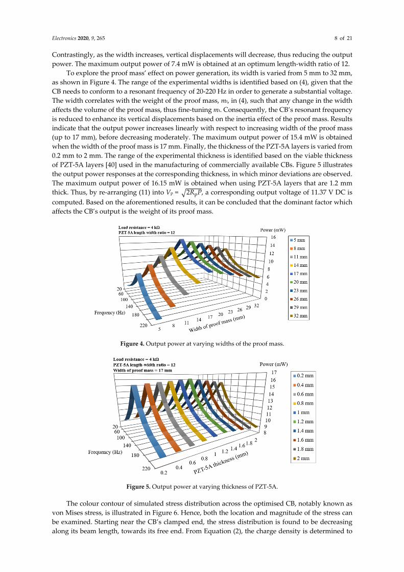
Contrastingly, as the width increases, vertical displacements will decrease, thus reducing the output power. The maximum output power of 7.4 mW is obtained at an optimum length-width ratio of 12.
To explore the proof mass’ effect on power generation, its width is varied from 5 mm to 32 mm, as shown in Figure 4. The range of the experimental widths is identified based on (4), given that the CB needs to conform to a resonant frequency of 20-220 Hz in order to generate a substantial voltage. The width correlates with the weight of the proof mass, mt, in (4), such that any change in the width affects the volume of the proof mass, thus fine-tuning mt. Consequently, the CB’s resonant frequency is reduced to enhance its vertical displacements based on the inertia effect of the proof mass. Results indicate that the output power increases linearly with respect to increasing width of the proof mass (up to 17 mm), before decreasing moderately. The maximum output power of 15.4 mW is obtained when the width of the proof mass is 17 mm. Finally, the thickness of the PZT-5A layers is varied from 0.2 mm to 2 mm. The range of the experimental thickness is identified based on the viable thickness of PZT-5A layers [40] used in the manufacturing of commercially available CBs. Figure 5 illustrates the output power responses at the corresponding thickness, in which minor deviations are observed. The maximum output power of 16.15 mW is obtained when using PZT-5A layers that are 1.2 mm thick. Thus, by re-arranging (11) into Vp = 2RpP, a corresponding output voltage of 11.37 V DC is computed. Based on the aforementioned results, it can be concluded that the dominant factor which affects the CB’s output is the weight of its proof mass.
Figure 4. Output power at varying widths of the proof mass.
Figure 5. Output power at varying thickness of PZT-5A.
The colour contour of simulated stress distribution across the optimised CB, notably known as von Mises stress, is illustrated in Figure 6. Hence, both the location and magnitude of the stress can be examined. Starting near the CB’s clamped end, the stress distribution is found to be decreasing along its beam length, towards its free end. From Equation (2), the charge density is determined to

Electronics 2020, 9, 265 9 of 21
be proportional to the distributed stress, therefore maximum charge density can be found near the clamped end. Minimum stress is indicated at the tip of the free end with a magnitude of 16.2 N/m2, whereas maximum stress is indicated near the clamped end, with a magnitude of 1.98 × 10⁷ N/m2. As such, both magnitudes depict a positive response towards dynamic loading.
Figure 6. Stress distribution of the optimised CB at 120 Hz.
Table 4 presents the optimised parameters that have been acquired from the CB’s simulation-based optimisation. They will be utilised as reference data for setting the input conditions of the proposed SPDS in PSCAD/EMTDC.
Table 4. Parameters of the optimised CB.
Parameters Symbols Values Geometric
PZT-5A dimensions lp × bp × hp 84 mm × 7 mm × 1.2 mm Copper dimensions lc × bc × hc 84 mm × 7 mm × 2 mm
Proof mass dimensions lt × bt × ht 5 mm × 17 mm × 5 mm Proof mass mt 0.0082 kg Mechanical
Input acceleration Ain 9.81 m/s2 Damping ratio ζ 0.001
Resonant Frequency fr 120 Hz Von Mises stress (max.) σy,max 1.98 × 10⁷ N/m2 Von Mises stress (min.) σy,min 16.2 N/m2
Electrical Output voltage Vp 11.37 V DC Output power P 16.15 mW
4. Proposed Self-Powered Dynamic System
4.1. System Overview
Figure 7 presents the proposed SPDS for mechanical-to-electrical energy conversion based on wind-enhanced vibration of the optimised CB. Its design is conceived with respect to Table 4 and deployment feasibility at an above-ground MRT train station in Khatib, Singapore, where the wind speed ranges from 6 m/s to 8 m/s, and the structural vibration frequency is 119.58 Hz during non-peak operating hours [42,43]. The CB is interfaced with the impedance (qZS) network’s input to provide an input power of 16.15 mW and an initial input voltage of 11.37 V DC. Using a proportional-integral based boost controller (PI-based BC), line RMS voltage at the three-phase inverter’s output is detected for feedback control to tune the shoot-through duty ratio of the qZSI-based PVEH, consequently tuning its DC-link voltage (Vboost) to obtain the boost factor.

Electronics 2020, 9, 265 10 of 21
Figure 7. Block diagram of the proposed SPDS.
Hence, the fluctuating voltage from the qZS network’s input will be stepped up with respect to a reference line RMS voltage of 40.28 V AC at the three-phase inverter’s output by utilising the obtained boost factor. A rectifier circuit is interfaced with the three-phase inverter for AC-to-DC rectification before transferring power to a 16.15 mW DC load through a filter capacitor. The SPDS adopts the non-isolated DC-DC converter topology so that the input and output of the power stage will share a common ground, allowing current to flow between them. Thus, the entire SPDS circuitry, including PI-based BC, is capable of being self-powered by the rectified voltage from the CB upon detecting vibrations. The designated 16.15 mW rating is suitable for powering miniature electronic devices used in the MRT train station; notably the infrared (IR) diode laser modules [44] that are installed at entry-exit gantries for motion detection of train commuters.
4.2. Control Methodology
The proposed PI-based BC for the SPDS is sub-divided into three control units, namely the inverter control unit, boost control unit and shoot-through control unit. Figure 8 illustrates the functionality of the inverter control unit. A PI controller is engaged to compare the three-phase inverter’s output voltage (Vq) with its desired line RMS value, namely the reference voltage (Vq,ref) before deriving an error signal (Vq,err) for required adjustments. Vq is also assigned at the PI controller’s output as a controller bias to serve as a constant offset for the adaptive proportional and integral gains (Kp and Ki). This ensures consistency in the adjusted voltage (Vq,adj) throughout the SPDS’s operation.
Figure 8. Inverter control unit of the PI-based BC.
Figure 9 illustrates the functionality of the boost control unit, which aims to obtain the boost factor (B) required for voltage step-up through DC-link voltage (Vboost) management. Firstly, Vq,adj is converted into Vboost using the line RMS-to-DC voltage conversion algorithm. Vboost is then divided by the qZS network’s input voltage (Vin) to obtain B, which is curtailed through a limiter. The limiter’s usage is attributed to the need to maintain a constant Vboost in order to attain the desired load (output)

Electronics 2020, 9, 265 11 of 21
voltage. Hence, regardless of Vin deviation from its initial value of 11.37 V DC during wind-enhanced vibration of the CB, B will vary accordingly to perform voltage step-up.
Figure 9. Boost control unit of the PI-based BC.
Equation (12) elaborates on B curtailment, where the minimum boost factor (Bmin) and maximum boost factor (Bmax) have been identified against the available Vin region before Vboost was finalised:
(Bmin) 1 B 5 (Bmax). (12)
Using the shoot-through control unit shown in Figure 10, B is engaged as a determinant of the shoot-through duty ratio (DZ) in order to initiate the SBC method for shoot-through pulse generation. The SBC method involves traditional PWM switching sequences, whereby square wave is used as a reference signal (Vref) while the triangular wave is used as a carrier signal (Vcarrier). These signals are compared with each other using two horizontal lines known as the upper limit (Vupp) and lower limit (Vlow) respectively. If Vcarrier is greater than Vupp or lower than Vlow, the IGBTs in each of the three-phase inverter’s leg will be shorted synchronously to generate shoot-through pulses, hence adjusting DZ autonomously. As such, Vboost constancy is enforced to influence B.
Figure 10. Shoot-through control unit of the PI-based BC.
Equation (13) depicts the corresponding logic-based algorithm for generating shoot-through pulses, which will be combined with the respective phases of Vref to form the IGBTs’ gate switching pulses:
Shoot-Through Pulse = ⎩⎨⎧ 1, Vcarrier Vupp
1, Vcarrier Vlow1, Vref = 1
0, Otherwise
. (13)
Figure 11 projects the qZSI’s PWM switching sequences derived from the SBC method. Assuming that the switching period is Tsw, the shoot-through period is TZ and non-shoot-through period is TNZ, DZ can be expressed as:
DZ = B − 12B =
TZ
Tsw (14)
in which:
Tsw = 1
fsw = TZ + TNZ (15)
where fsw is the corresponding switching frequency to determine Tsw.

Electronics 2020, 9, 265 12 of 21
Figure 11. PWM switching sequences for qZSI operation.
4.3. Design of qZS Network Inductors and Capacitors
Formulations to determine inductor and capacitor ratings in the qZS network are strictly dependent on compatibility with Vin, where B, current stress and voltage stress might become maximised during voltage step-up operations, affecting Vboost stability. Conjointly, maximum shoot-through period (TZ,max) tend to occur, allowing maximum current (IL,max) to pass through the inductors, hence establishing maximum current ripple. To address the aforementioned practical concerns, 10% peak-to-peak current ripple is strategically selected for the inductors (rc% = 10%). Since the capacitors tend to charge the inductors through their current during the shoot-through state, current ripple will be mostly absorbed while voltage ripple is minimised on the three-phase inverter bridge in order to stabilise Vboost. Therefore, 0.9% voltage ripple is strategically selected for the capacitors (rv% = 0.9%).
Equation (16) defines the relation between the inductors’ average current (IL), load power (Pload) and Vin. Of which, IL is used to identify the permissible value of IL,max in the qZS inductors by engaging rc% in Equation (17):
IL = Pload
Vin (16)
IL,max = IL + ILrc%
2 (17)
Through equations (16–20), a trend is observed in the qZS network’s efficiency, where it is possible to retain inductance and capacitance values without attenuating rc% and rv%. Contrastingly, attenuation of rc% and rv% requires an impractical approach whereby the inductors and capacitors have to be interchanged in conjunction with Vin fluctuations. Therefore, the key approach is to identify the permissible value of TZ,max:
TZ,max = 1 − Bmax
-1
TZ -1 (18)
which constitutes:
L1 = L2 = TZ,max
2MVin
IL,maxrc% (19)
C1 = C2 = TZ,max
22IL
BmaxVinrv% (20)
in which:

Electronics 2020, 9, 265 13 of 21
M = TNZ
TNZ − TZ (21)
where M is the modulation index of Vcarrier, thus correlating with SBC formulations in (14) and (15) due to TZ and TNZ involvement. From equations (19) and (20), it is clear that determining the inductor ratings (L1, L2) and capacitor ratings (C1, C2) involves the concise formulation of TZ,max, since it also affects the transient response of the qZSI [21–26]. Undesirable TZ,max precipitates increased ripple in inductor currents and capacitor voltages, as well as severe clipping of Vboost. From Equation (18), it is determined that the exceedance of Bmax will cause Vboost to be forcibly constrained, thus propagating severe clipping.
4.4. Simulation Model Specifications
Tables 5–7 present the respective simulation model specifications [45,46] of the proposed SPDS in PSCAD/EMTDC. Notably, the Vin available range (11.37-20.31 V DC) was identified with reference to Table 4 and the voltage generation potential of the CB during wind-enhanced vibrations, as validated by simulation evaluations in Section 5. To emulate arbitrary wind speed at the above-ground MRT train station in Khatib, Singapore, a wind source is interfaced with the CB through a limiter as shown in Figure 12, functioning as an external input. The limiter is engaged to maintain the arbitrary wind speed at 6-8 m/s, therefore matching actual arbitrary wind speed. Moreover, the wind source is configured to generate variegated wind components that constitute the arbitrary wind speed; namely mean wind speed, gust, ramp, and noise. Table 8 provides a formalised depiction of these wind components using data collected from the above-ground MRT train station [42].
Table 5. Specifications of the SPDS.
Parameters Symbols Values Load power Pload 16.15 mW
Input voltage Vin 11.37-20.31 V DC DC-link voltage Vboost 56.85 V DC Output voltage Vout 54.4 V DC
Switching frequency fsw 45 kHz qZS inductors L1, L2 81 uH qZS capacitors C1, C2 20 nF
Current ripple of qZS inductors rc% 10% Voltage ripple of qZS capacitors rv% 0.9%
Output filter capacitor Cout 1 mF
Table 6. 1N5711 Schottky diode (D0) specifications.
Parameters Symbols Values Absolute maximum ratings Repetitive reverse voltage VRRM 70 V
Forward continuous current IF,CO 15 mA Power dissipation PD 430 mW
Electrical characteristics Reverse breakdown voltage VBR 70 V
Forward voltage VF 0.41 V Reverse current IR 0.2 uA

Electronics 2020, 9, 265 14 of 21
Table 7. FGD3325G2-F085 IGBT (S1-S6) specifications.
Parameters Symbols Values Absolute maximum ratings
Collector-emitter breakdown voltage VCE,BR 250 V Emitter-collector reverse voltage VCE,R 28 V Gate-emitter continuous voltage VGE,CO ±10 V
Collector continuous current IC,CO 41 A Power dissipation PD 150 W
Electrical characteristics Collector-emitter saturation voltage VCE,SAT 1.68 V
Collector-emitter leakage current ICE,LK 1 mA Emitter-collector leakage current IEC,LK 1 mA
Gate charge QG 21 nC
Figure 12. qZSI-based PVEH adopting wind source in PSCAD/EMTDC.
Table 8. Arbitrary wind speed data input for the wind source.
Parameters Values Arbitrary wind speed 6-8 m/s
Mean wind speed 7 m/s Gust
Gust peak velocity 0.2 m/s Gust period 0.13 s
Gust start-time 0.05 s Ramp
Ramp maximum velocity 0.45 m/s Ramp period 0.12 s
Ramp start-time 0.1 s Noise
Number of noise components 50 Surface drag coefficient 0.02
Turbulence scale 0.03 m 5. Simulation Results and Analyses
Using PSCAD/EMTDC as a testbed to model the proposed SPDS, simulation evaluations are presented to observe corresponding transient responses and load-following performances where Vin fluctuates in conjuncture with arbitrary wind speed directed at the CB during vibration-based operation. The aforementioned proceedings constitute wind-enhanced vibration effects that emulate the SPDS’s deployment at the above-ground MRT train station in Khatib, Singapore, where its daily

Electronics 2020, 9, 265 15 of 21
recorded ambient data depicts an arbitrary wind speed of 6-8 m/s and a structural vibration frequency of 119.58 Hz during non-peak operating hours. In order to demonstrate the dynamic responsiveness of the SPDS, it is modelled at a simulation run-time of 5 seconds.
Figure 13 depicts the transient response of the three-phase inverter’s output voltage (Vq) and adjusted voltage (Vq,adj) when matching the reference voltage (Vq,ref) during feedback control. It is apparent that the adaptive proportional and integral gains (Kp = 0.03, Ki = 90.91 × 10⁻⁶) of the PI-based BC have piloted fast settling-time response with negligible steady-state error, defining respective scalar gain at different time-step to quickly secure 49 V AC for Vq,adj. Notably, Vq,adj is strategically attenuated to anticipate accumulated losses (i.e., conduction loss and switching loss), hence attributing the desired 40.28 V AC for Vq after incurring these losses. Conjointly, maximum peak overshoot is decreased due to low Kp, while residual errors are mitigated using Ki to complement Kp.
Figure 13. Voltage transients at the three-phase inverter’s output.
Figure 14 depicts the fundamental operation of the qZSI-based PVEH when the CB is controlled to wind-enhanced vibrations. It is observed that the boost factor (B) consistently attenuates to step-up the input voltage (Vin) which randomly deviates from 11.37 V DC to 20.31 V DC due to variegated wind components of the arbitrary wind speed. As evidenced in Figure 14(b), B manages to conform to its respective limits in (12) with respect to the DC-link voltage (Vboost) attained from Vq,adj conversion in the PI-based BC’s boost control unit. Such attenuation involving B aims to secure a constant Vboost of 56.85 V DC despite Vin fluctuation during uncertain output performances of the CB. Figure 15 validates this analogy to a large extent since minor clipping (i.e., 2.4%) is found in Vboost when observing its voltage transient. Moreover, minimisation of clipping is attributed by low inductor and capacitor ratings in the qZS network; which were determined based on the permissible maximum shoot-through period (TZ,max), since TZ,max prevents Vboost from being forcibly constrained.

Electronics 2020, 9, 265 16 of 21
Figure 14. qZSI-based PVEH operation during uncertain output performances of the CB: (a) Fluctuation of input voltage. (b) Corresponding boost factor for voltage restoration at DC-link.
Figure 15. DC-link voltage: (a) Voltage waveform. (b) Zoomed-in voltage transient of the waveform.
Figure 16 depicts the transient response of the inductors (L1, L2) and capacitors (C1, C2) in the qZS network, specifically their ripple characteristics. It is evident that the determined ratings for these components have rendered consistency in the inductor currents (IL1, IL2) and capacitor voltages (VC1, VC2), strictly conforming to the selected 10% peak-to-peak inductor current ripple and 0.9% capacitor voltage ripple respectively. Furthermore, it is observed in Figure 16(a) that the measured average inductor current (IL) and maximum inductor current (IL,max) correlates with their theoretical formulations in equations (16) and (17). The strategic acquisition of both currents synchronises

Electronics 2020, 9, 265 17 of 21
optimised charging and discharging sequences between the capacitors and inductors as depicted. Therefore, Vboost stability is enforced throughout the shoot-through and non-shoot-through periods initiated by the aforementioned sequences.
Figure 16. Transient response of respective passive components in the qZS network: (a) Inductor currents. (b) Capacitor voltages.
Figure 17 presents the measured output voltage (Vout) and load power (Pload) of the SPDS. Both measurements proved that successful integration of the PI-based BC in the SPDS has established viable load-following synchronisation across all sub-systems to secure 54.4 V DC for Vout, which constitutes Pload measured value of 14.8 mW. Given that the SPDS’s input power is equivalent to Pload rated value of 16.15 mW, its computed efficiency ƞ is 91.64% based on: ƞ = [Pload (measured) / Pload (rated)] × 100%. It is also apparent that there is almost no distortion of Vout and Pload, thus further validating the PI-based BC’s excellent control functionality. Figure 18 illustrates the efficiency characteristics of the CB and SPDS when experimented against different DC load sizes. It is observed that the respective efficiencies are proportional to each other due to synchronised operations from the CB to the entirety of the SPDS, peaking at the rated load power of 16.15 mW before deteriorating. This is attributed by the limited B, which impairs the SPDS’s output power since Vout is required to be increased at larger loads. Furthermore, the SPDS tend to have lower efficiency in comparison to the CB as a result of cumulative losses across its circuitry.

Electronics 2020, 9, 265 18 of 21
Figure 17. Measured electrical outputs of the SPDS: (a) Output voltage. (b) Load power.
Figure 18. Computed efficiency versus rated power of different loads.
6. Conclusions
This paper has presented analytical modelling, control, and performance evaluations on perceiving the operability of a novel SPDS that incorporates qZSI-based PVEH in its framework. Extensive optimisation of a CB was performed in COMSOL Multiphysics to maximise its power generation capability, followed by the conceptualisation of the SPDS’s specifications in respect of the CB’s optimised parameters. Conjointly, a modified control scheme (i.e., PI-based BC) derived from the SBC method was devised to resolve voltage inadequacies at the qZSI-based PVEH during uncertain output performances of the CB, establishing interoperability across the SPDS to maximise power transfer to a DC load. The acquired simulation results from PSCAD/EMTDC have validated theoretical-based design formulations of the SPDS when it was tested for deployment feasibility. Fast settling-time, negligible steady-state error, minimal distortion, minor clipping as well as adherence to pre-set ripple characteristics were observed at respective simulated transient outputs. Thus, high efficiencies of 94.07% and 91.64% were attained by the CB and SPDS respectively, after alleviating cumulative losses in the qZSI-based PVEH. Due to the novelty of the qZSI-based PVEH in SPDSs,

Electronics 2020, 9, 265 19 of 21
future extension of this work may include devising a control scheme that allows higher boost factor manipulation without inducing increased clipping across the DC-link voltage.
Author Contributions: Conceptualisation, W.Q.T.P.; methodology, W.Q.T.P.; software, W.Q.T.P.; validation, W.Q.T.P. and M.R.B.M.S.; formal analysis, W.Q.T.P.; investigation, W.Q.T.P.; resources, R.T.N.; data curation, M.R.B.M.S.; writing—original draft preparation, W.Q.T.P.; writing—review and editing, M.R.B.M.S. and R.T.N.; visualisation, W.Q.T.P.; supervision, R.T.N.; project administration, M.R.B.M.S. All authors have read and agreed to the published version of the manuscript.
Funding: This research received no external funding. The APC for this paper is waived as it is a Feature Paper invited by the guest editor.
Conflicts of Interest: The authors declare no conflict of interest.
References
1. Podder, P.; Constantinou, P.; Mallick, D.; Amann, A.; Roy, S. Magnetic Tuning of Nonlinear MEMS Electromagnetic Vibration Energy Harvester. J. Microelectromech. Syst. 2017, 26, 539–549.
2. Xia, H.; Xia, Y.; Ye, Y.; Qian, L.; Shi, G. Simultaneous Wireless Strain Sensing and Energy Harvesting From Multiple Piezo-Patches for Structural Health Monitoring Applications. IEEE Trans. Ind. Electron. 2019, 66, 8235–8243.
3. Yan, B.; Zhang, C.; Li, L. Design and Fabrication of a High-Efficiency Magnetorestrictive Energy Harvester for High-Impact Vibration Systems. IEEE Trans. Magn. 2015, 5, 1–4.
4. Zhang, Z.; Kan, J.; Wang, S.; Wang, H.; Yang, C.; Chen, S. Performance Dependence on Initial Free-End Levitation of a Magnetically Levitated Piezoelectric Vibration Energy Harvester with a Composite Cantilever Beam. IEEE Access, 2017, 26, 27563–27572.
5. Nabavi, S.; Zhang, L. Nonlinear Multi-Mode Wideband Piezoelectric MEMS Vibration Energy Harvester. IEEE Sensors J. 2019, 19, 4837–4848.
6. Sriramdas, R.; Pratap, R. Scaling and Performance Analysis of MEMS Piezoelectric Energy Harvesters. J. Microelectromech. Syst. 2017, 26, 679–690.
7. Poh, W.Q.T.; Saifuddin, M.R.B.M.; Logenthiran, T. Design and Simulation of a Piezoelectric Cantilever Beam for Mechanical Vibration Energy Harvesting. In Proceedings of the 2018 IEEE Innovative Smart Grid Technologies Asia Conference, Singapore, 22–25 May 2018.
8. Jia, Y.; Seshia, A.A. Power Optimization by Mass Tuning for MEMS Piezoelectric Cantilever Vibration Energy Harvesting. J. Microelectromech. Syst. 2016, 25, 108–117.
9. Abasian, A.; Tabesh, A.; Nezhad, A.Z.; Rezaei-Hosseinabadi, N. Design Optimization of an Energy Harvesting Platform for Self-Powered Wireless Devices in Monitoring of AC Power Lines. IEEE Trans. Power Electron. 2018, 33, 10308–10316.
10. Lei, A.; Xu, R.; Borregaard, L.M.; Guizzetti, M.; Hansen, O.; Thomsen, E.V. Impedance Based Characterization of a High-Coupled Screen Printed PZT Thick Film Unimorph Energy Harvester. J. Microelectromech. Syst. 2014, 23, 842–854.
11. Zheng, X.; Zhang, Z.; Zhu, Y.; Mei, J.; Peng, S.; Li, L.; Yu, Y. Analysis of Energy Harvesting Performance for d15 Mode Piezoelectric Bimorph in Series Connection Based on Timoshenko Beam Model. IEEE/ASME Trans. Mechatronics, 2015, 2, 728–739.
12. Ghoddus, H.; Kordrostami, Z. Harvesting the Ultimate Electrical Power from MEMS Piezoelectric Vibration Energy Harvesters: An Optimization Approach. IEEE Sensors J. 2018, 18, 8667–8675.
13. Yang, Z.; Zu, J.; Xu, Z. Reversible Nonlinear Energy Harvester Tuned by Tilting and Enhanced by Nonlinear Circuits. IEEE/ASME Trans. Mechatronics, 2016, 21, 2174–2184.
14. Chamanian, S.; Ulusan, H.; Koyuncuoglu, A.; Muhtaroglu, A.; Kulah, H. An Adaptable Interface Circuit with Multistage Energy Extraction for Low-Power Piezoelectric Energy Harvesting MEMS. IEEE Trans. Power Electron. 2019, 34, 2739–2747.
15. Miller, L.M.; Elliot, A.D.T.; Mitcheson, P.D.; Halvorsen, E.; Paprotny, I.; Wright, P.K. Maximum Performance of Piezoelectric Energy Harvesters when Coupled to Interface Circuits. IEEE Sensors J. 2016, 16, 4803–4815.
16. Sankman, J.; Ma, D. A 12-µW to 1.1-mW AIM Piezoelectric Energy Harvester for Time-Varying Vibrations with 450-nA IQ. IEEE Trans. Power Electron. 2015, 30, 632–643.

Electronics 2020, 9, 265 20 of 21
17. Kong, N.; Ha, D.S. Low-Power Design of a Self-Powered Piezoelectric Energy Harvesting System with Maximum Power Point Tracking. IEEE Trans. Power Electron. 2012, 27, 2298–2308.
18. Du, S.; Amaratunga, G.A.J.; Seshia, A.A. A Cold-Startup SSHI Rectifier for Piezoelectric Energy Harvesters with Increased Open-Circuit Voltage. IEEE Trans. Power Electron. 2019, 34, 263–274.
19. Savarimuthu, K.; Sankararajan, R.; Murugesan, S. Analysis and Design of Power Conditioning Circuit for Piezoelectric Vibration Energy Harvester. IET Sci., Measurement & Technol. 2017, 11, 723–730.
20. Chen, N.; Wei, T.; Ha, D.S.; Jung, H.J.; Lee, S. Alternating Resistive Impedance Matching for an Impact-Type Microwind Piezoelectric Energy Harvester. IEEE Trans. Ind. Electron. 2018, 65, 7374–7382.
21. Zdanowski, M.; Peftitsis, D.; Piasecki, S.; Rabkowski, J. On the Design Process of a 6-kVA Quasi-Z-Inverter Employing SiC Power Devices. IEEE Trans. Power Electron. 2016, 31, 7499–7508.
22. Liu, Y.; Abu-Rub, H.; Ge, B. Front-End Isolated Quasi-Z-Source DC-DC Converter Modules in Series for High-Power Photovoltaic Systems-Part 1: Configuration, Operation, and Evaluation. IEEE Trans. Ind. Electron. 2017, 64, 347–358.
23. Zhang, Y.; Shi, J.; Zhou, L.; Li, J.; Sumner, M.; Wang, P.; Xia, C. Wide Input-Voltage Range Boost Three-Level DC-DC Converter with Quasi-Z-Source for Fuel Cell Vehicles. IEEE Trans. Power Electron. 2017, 32, 6728–6738.
24. Chub, A.; Husev, O.; Blinov, A.; Vinnikov, D. Novel Isolated Power Conditioning Unit for Micro Wind Turbine Applications. IEEE Trans. Ind. Electron. 2017, 64, 5984–5993.
25. Shinde, U.K.; Kadwane, S.G.; Gawande, S.P.; Reddy, M.J.B.; Mohanta, D.K. Sliding Mode Control of Single-Phase Grid-Connected Quasi-Z-Source Inverter. IEEE Access, 2017, 5, 10232–10240.
26. Poh, W.Q.T.; Saifuddin, M.R.B.M.; Logenthiran, T. A Comparative Analysis between Z-Source and Quasi-Z-Source Inverters for Boost Operation. In Proceedings of the 2018 Asian Conference on Energy, Power and Transportation Electrification (ACEPT), Singapore, 30 October 2018 – 2 November 2018.
27. Noroozi, N.; Zolghadri, M.R. Three-Phase Quasi-Z-Source Inverter with Constant Common-Mode Voltage for Photovoltaic Application. IEEE Trans. Ind. Electron. 2018, 65, 4790–4798.
28. Jagan, V.; Kotturu, J.; Das, S. Enhanced-Boost Quasi-Z-Source Inverters with Two-Switched Impedance Networks. IEEE Trans. Ind. Electron. 2017, 64, 6885–6897.
29. Naayagi, R.T.; Panda, S.K. Fault-Tolerant Converter for Future Offshore Wind Farm HVDC Networks. In Proceedings of the 2017 IEEE Innovative Smart Grid Technologies Asia Conference, Auckland, New Zealand, 4–7 December 2017.
30. Nguyen, M-K.; Lim, Y-C.; Park, S-J. A Comparison between Single-Phase Quasi-Z-Source and Quasi-Switched Boost Inverters. IEEE Trans. Ind. Electron. 2015, 62, 6336–6344.
31. Liu, Y.; Ge, B.; Abu-Rub, H.; Peng, F.Z. An Effective Control Method for Three-Phase Quasi-Z-Source Cascaded Multilevel Inverter Based Grid-Tie Photovoltaic Power System. IEEE Trans. Ind. Electron. 2014, 61, 6794–6802.
32. Nguyen, M-K.; Choi, Y-O. PWM Control Scheme for Quasi-Switched-Boost Inverter to Improve Modulation Index. IEEE Trans. Power Electron. 2018, 33, 4037–4044.
33. Liang, W.; Liu, Y.; Ge, B.; Abu-Rub, H. Investigation on Pulse-Width Amplitude Modulation-Based Single-Phase Quasi-Z-Source Photovoltaic Inverter. IET Power Electron. 2017, 10, 1810–1818.
34. Kang, M-G.; Jung, W-S.; Kang, C-Y.; Yoon, S-J. Recent Progress on PZT Based Piezoelectric Energy Harvesting Technologies. Actuators, 2016, 5, 1–17.
35. Dechant, E.; Fedulov, F.; Fetisov, L.Y.; Shamonin, M. Bandwidth Widening of Piezoelectric Cantilever Beam Arrays by Mass-Tip Tuning for Low-Frequency Vibration Energy Harvesting. Applied Sciences, 2017, 7, 1–16.
36. Thein, C.K.; Ooi, B.L.; Liu, J-S.; Gilbert, J.M. Modelling and Optimisation of a Bimorph Piezoelectric Cantilever Beam in an Energy Harvesting Application. J. Eng. Sci. Technol. 2016, 11, 212–227.
37. Hao, B.; Zhu, Z.; Zhou, P.; Li, W. A Study of the Properties of a Piezoelectric Ceramic Plate in the Symmetric Fixation Mode. IEEE Access, 2018, 6, 36863–36873.
38. Raju, G.K.S.P.; Kumar, P.A.; Rao, K.S.; Aravapalli, V. Design and Simulation of a Cantilever Beam Based MEMS Bimorph Piezoelectric Energy Harvester. Mechanics, Material Sci. Eng. J. 2017, 9, 1–7.
39. Constanzo, L.; Schiavo, A.L.; Vitelli, M. Power Extracted From Piezoelectric Harvesters Driven by Non-Sinusoidal Vibrations. IEEE Trans. Circuits Syst. I, Reg. Papers 2019, 66, 1291–1303.

Electronics 2020, 9, 265 21 of 21
40. Piezoelectric Sheets and Plates, Mide Technology. Available online: https://piezo.com/collections/piezo-sheets-plates?_=pf&pf_t_quantity=Quantity__1&pf_t_piezo_material=Piezo%20Material__PZT%205A (accessed on 16 July 2019).
41. Mouser Electronics Singapore. Available online: https://www.mouser.sg/datasheet/2/308/1N5822-1305059.pdf (accessed on 21 October 2019).
42. Singapore Land Transport Authority. Available online: https://www.mytransport.sg/content/mytransport/home/dataMall.html (accessed on 9 August 2019).
43. Singapore Mass Rapid Transit (SMRT) Corporation Ltd. Available online: http://www.smrttrains.com.sg/News-Room/Statistics-Data (accessed on 9 August 2019).
44. MXTLASER Technology Corporation. Available online: http://www.mxtlaser.com/product/830nm-IR-Diode-Laser-Module.html (accessed on 5 October 2019).
45. Mouser Electronics Singapore. Available online: https://www.mouser.sg/datasheet/2/389/1n5711-954385.pdf (accessed on 21 October 2019).
46. Mouser Electronics Singapore. Available online: https://www.mouser.sg/datasheet/2/308/FGD3325G2_F085-1123649.pdf (accessed on 13 November 2019).
© 2020 by the authors. Licensee MDPI, Basel, Switzerland. This article is an open access article distributed under the terms and conditions of the Creative Commons Attribution (CC BY) license (http://creativecommons.org/licenses/by/4.0/).


![QUASI-BIGEBRES DE LIE ET ALGEBRES QUASI-BATALIN ...streaming.ictp.it/preprints/P/99/174.pdf3 Quasi-bigebres de Lie Les quasi-bigebres de Lie [6] (appelees quasi-bigebres jacobiennes](https://static.fdocuments.net/doc/165x107/60aa5fd4a787df4f051abfc1/quasi-bigebres-de-lie-et-algebres-quasi-batalin-3-quasi-bigebres-de-lie-les.jpg)