A New Thermal Management Material for HBLEDs based · PDF fileA New Thermal Management...
7
A New Thermal Management Material for HBLEDs based on Aluminum Nitride Ceramics Thermal Management Challenges in HBLED Excess heat leads to a whole range of performance and reliability issues for high power semiconductor applications such as high brightness LEDs (HBLED). Because HBLED light output is sensitive to heat, as an LED gets too hot, more input energy is converted to heat instead of light, which further increases the LED temperature leading to the potential of catastrophic failure. Figure 1 from Cary Escow at Lightspeed 1 shows the degradation of light output as a function of HBLED junction temperature. L 70 refers to the point where the current light output of the LED is 70% of the original light output (at L 50 the light output falls to 50%). This example illustrates clearly the critical importance of pulling heat away from the HBLED in order to ensure a low junction temperature and stable light output. Role of Packaging and Packaging Materials From the view point of z direction thermal conduction (direction from the diode junction heat source toward the heat sink) and x,y direction heat spreading, the closer to the semiconductor junction, the more critical the material’s role in heat management. Thus, in order of importance, we can roughly rank device and packaging material thermal conductivity requirements: 1.Semiconductor material below the junction (for non-flip chip applications) 2.Die attach material 3.First level of packaging (conduction and heat spreading) 4.TIM or solder between first level of packaging and board level 5.Board level packaging (conduction and heat spreading) 6.TIM or solder between board and heat sink 7.Heat sink or heat spreader 1 1 Cary Escow, Avnet Lightspeed Newletter
Transcript of A New Thermal Management Material for HBLEDs based · PDF fileA New Thermal Management...

A New Thermal Management Material for HBLEDs based on Aluminum Nitride Ceramics
Thermal Management Challenges in HBLEDExcess heat leads to a whole range of performance and reliability issues for high power semiconductor applications such as high brightness LEDs (HBLED).
Because HBLED light output is sensitive to heat, as an LED gets too hot, more input energy is converted to heat instead of light, which further increases the LED temperature leading to the potential of catastrophic failure. Figure 1 from Cary Escow at Lightspeed1 shows the degradation of light output as a function of HBLED junction temperature. L70 refers to the point where the current light output of the LED is 70% of the original light output (at L50 the light output falls to 50%).
This example illustrates clearly the critical importance of pulling heat away from the HBLED in order to ensure a low junction temperature and stable light output.
Role of Packaging and Packaging MaterialsFrom the view point of z direction thermal conduction (direction from the diode junction heat source toward the heat sink) and x,y direction heat spreading, the closer to the semiconductor junction, the more critical the material’s role in heat management. Thus, in order of importance, we can roughly rank device and packaging material thermal
conductivity requirements:1.Semiconductor material below the junction (for non-flip chip applications)2.Die attach material3.First level of packaging (conduction and heat spreading)4.TIM or solder between first level of packaging and board level5.Board level packaging (conduction and heat spreading)6.TIM or solder between board and heat sink7.Heat sink or heat spreader
1
1 Cary Escow, Avnet Lightspeed Newletter

This simple discussion makes it very clear how critical the first level of packaging is to thermal management of high power devices, which helps to explain the significant use of ceramic
materials as a first level packaging material for HBLED. Figure 2(a)2 shows the basic packaging configuration for HBLED with a ceramic material as the first level package.
Figure 2(b)3 shows a schematic of the packaged HBLED bonded to a metal core printed circuit board (MCPCB) and heat sink which illustrates the entire thermal path starting with the HBLED junction.
Table 1 below shows the different types of ceramics used for LED applications as well as some of the basic thermal properties of these ceramic materials.
2
2 Luxeon from Philips Lumileds
3 Luxeon mounting guide from Philips Lumileds

Application Ceramic Thermal Conductivity
(W/m-K)
Packaging Technology
Ceramic Cost Factor
First level HBLED
package
Al2O3 (96%) 20 W/m-K Direct Plated Copper (DPC)
1
AlN (95%) 170 W/m-K minimum
Direct Plated Copper (DPC)
>8
For this table, the cost multiple of the various ceramic technologies compared to alumina is provided. Note that this is not the package cost but the cost of the ceramic component of the package.
Aluminum Nitride- Right Technical Solution But Too ExpensiveAluminum Nitride (AlN) is an ideal choice for high thermal demand applications because of its combination of high thermal conductivity and mid range CTE of 4.5 ppm/C; but AlN’s >8 times cost factor relative to aluminum oxide limits its application significantly. AlN is currently used in HBLED packaging, but only in situations where there is no other feasible alternatives. The high cost pressure in the HBLED market and the significant portion of total device cost that packaging entails, increases the pressure to minimize high cost AlN usage.
AlN’s high cost comes from a number of factors. Some of the most significant are listed in the table below:
Cost Factor Comparison to Alumina Comments
AlN ceramics are fabricated from AlN powder, and AlN powder cost for typical electronic grade material is extremely high
AlN powder is 15 to 25 times more expensive then alumina powder
Electronic applications almost exclusively utilize high cost “carbo-thermally reduced” AlN powder
AlN ceramics are processed at very high temperatures. High temperature furnaces increase capital costs and decrease furnace throughput
Alumina is processed at 1450C to 1620C, AlN is processed at 1825C.
For alumina, continuous furnaces are available. For AlN, only batch graphite or refractory metal furnaces are available.
3
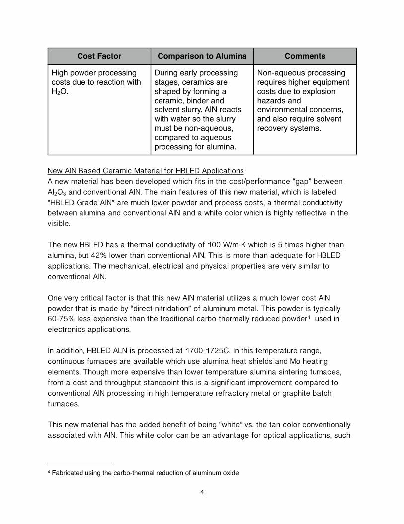
Cost Factor Comparison to Alumina Comments
High powder processing costs due to reaction with H2O.
During early processing stages, ceramics are shaped by forming a ceramic, binder and solvent slurry. AlN reacts with water so the slurry must be non-aqueous, compared to aqueous processing for alumina.
Non-aqueous processing requires higher equipment costs due to explosion hazards and environmental concerns, and also require solvent recovery systems.
New AlN Based Ceramic Material for HBLED ApplicationsA new material has been developed which fits in the cost/performance “gap” between Al2O3 and conventional AlN. The main features of this new material, which is labeled “HBLED Grade AlN” are much lower powder and process costs, a thermal conductivity between alumina and conventional AlN and a white color which is highly reflective in the visible.
The new HBLED has a thermal conductivity of 100 W/m-K which is 5 times higher than alumina, but 42% lower than conventional AlN. This is more than adequate for HBLED applications. The mechanical, electrical and physical properties are very similar to conventional AlN.
One very critical factor is that this new AlN material utilizes a much lower cost AlN powder that is made by “direct nitridation” of aluminum metal. This powder is typically 60-75% less expensive than the traditional carbo-thermally reduced powder4 used in electronics applications.
In addition, HBLED ALN is processed at 1700-1725C. In this temperature range, continuous furnaces are available which use alumina heat shields and Mo heating elements. Though more expensive than lower temperature alumina sintering furnaces, from a cost and throughput standpoint this is a significant improvement compared to conventional AlN processing in high temperature refractory metal or graphite batch furnaces.
This new material has the added benefit of being “white” vs. the tan color conventionally associated with AlN. This white color can be an advantage for optical applications, such
4
4 Fabricated using the carbo-thermal reduction of aluminum oxide

as HBLED, because the reflection of visible light is much higher. This reflection data across the visible spectrum is shown in Figure 3 below.
This figure shows Reflectance factor vs. wavelength for #1-Tan and #2-Grey conventional AlN ceramic samples and #3-White, HBLED grade AlN. Note the HBLED grade AlN reflects 70-80% through the visible spectrum, compared to about 30% for conventional material.
Figure 4 shows the white color of the HBLED AlN compared to conventional AlN substrates.
5

Table 3 below has more details about the properties of HBLED grade AlN. The mechanical and electrical properties of HBLED AlN is very similar to conventional higher cost AlN ceramics.
Property Value Comments
Thermal Conductivity (W/m-K)
100 (typical) Measured by laser flash
Electrical Resistivity (Ohm-cm)
>1012 (1014 is typical)
Flexural Strength (Mpa) 300 (typical) Four point bend test
Density (%) >97% (typical)
Visible Light Reflectivity (%) 70-80%
A comparison of the thermal performance of available ceramic packaging materials, (and undoped silicon for reference) measured using Laser Flash, including HBLED Grade AlN is shown in Figure 4 below.
6

What is Next?This article focusses on a new AlN ceramic technology that results in a material that from a cost/performance standpoint bridges the current wide gap between high thermal conductivity, high cost AlN; and lower thermal performance, lower cost aluminum oxide.
For the focus applications of this technology, specifically HBLED tiles, the 100W/m-K thermal performance is more than adequate. Due to the highly cost competitive nature of these applications, and the current high packaging costs for HBLED devices, there is a strong fit for a new material with significantly lower cost structure. As this material is adapted more widely, it is expected that it will compete favorably for many applications that are now served exclusively by aluminum oxide.
About CMCCMC Laboratories, Inc. (www.cmclaboratories.com) is an advanced materials development firm located in Tempe, Arizona. CMC specializes in developing new materials for electronic interconnect and packaging applications. CMC has applied for a patent to cover the technology described in this article and is now actively licensing this technology to interested manufacturers.
0
50
100
150
200
Alumina (96) Si3N4 AlN HBLED AlN Silicon
Ther
mal
Con
duct
ivity
W/m
-K
7