A NEW CONCEPT FOR THE REALIZATION' OF DATA … Bound... · OF DATA MODEMS WITH INTEGRATED DIGITAL...
21
R 796 , Philips Res. Repts 27, 223-243, 1972 A NEW CONCEPT FOR THE REALIZATION' OF DATA MODEMS WITH INTEGRATED DIGITAL FILTERS AND MODULATORS by P. E. LEUTHOLD Abstract The theory of a new kind of digital networks is outlined which are , composed of active elements and resistors only. The structures resemble a framework of digital transversal filters the taps of which are inter- connected by means of logic gates followed by weighing devices. The relations between input and output signals are described by convolu- tion integrals with multiple kernels or by corresponding multiple sums respectively. After a brief summary of nonrecursive digital-filter tech- niques the theory and the realization of digital networks with two-dimen-' sional convolution kernels are discussed. It is shown that this concept permits the design of fully integrated data transmitters (AM, SSB, PM, FM) with interesting properties. Some details of system errors are out- lined. An experimental single-sideband data transmitter is described, 1. Introduction The rapid increase in the use of digital circuits is due to the advances in integrated-circuit technology. Digital circuits require a fairly large number of elements. It is possible, however, to design these circuits by the only use of active elements and resistors, components that are well suited for monolithic construction in an integrated circuit. For that reason it is now possible to realize important parts of modern communication systems by means of large- scale integrated circuits (LS!). ! Indispensable parts of a transmission system are filters and modulators. In the last years much 'effort has been devoted to the use of digital circuits in filter design. A basic concept is the digitalized versio~ of the so-called "transversal filter" 1). It consists of a delay line which is tapped with resistors at fixed spots. The relation between the input voltage of the delay line and the sum of the resistively tapped currents depends on the values of the resistors, on the time intervals between adjoining taps, and on the number of taps. In such a manner it is possible to approximate any given transfer function in a certain frequency interval. Especially the realization of filters with exactly linear phase characteristic, a requirement to be often met in pulse-transmission sys- tems, can be easily achieved. The replacement of the delay line by a digital shift register yields the digital transversal filter 2.3): Naturally, the treatment of analog signals requires an analog-digital conversion preceding the digital filter. ,. The realization of modulators by means of digital circuits is rather simple
Transcript of A NEW CONCEPT FOR THE REALIZATION' OF DATA … Bound... · OF DATA MODEMS WITH INTEGRATED DIGITAL...

R 796,
Philips Res. Repts 27, 223-243, 1972
A NEW CONCEPT FOR THE REALIZATION'OF DATA MODEMS WITH INTEGRATEDDIGITAL FILTERS AND MODULATORS
by P. E. LEUTHOLD
AbstractThe theory of a new kind of digital networks is outlined which are, composed of active elements and resistors only. The structures resemblea framework of digital transversal filters the taps of which are inter-connected by means of logic gates followed by weighing devices. Therelations between input and output signals are described by convolu-tion integrals with multiple kernels or by corresponding multiple sumsrespectively. After a brief summary of nonrecursive digital-filter tech-niques the theory and the realization of digital networks with two-dimen-'sional convolution kernels are discussed. It is shown that this conceptpermits the design of fully integrated data transmitters (AM, SSB, PM,FM) with interesting properties. Some details of system errors are out-lined. An experimental single-sideband data transmitter is described,
1. Introduction
The rapid increase in the use of digital circuits is due to the advances inintegrated-circuit technology. Digital circuits require a fairly large number ofelements. It is possible, however, to design these circuits by the only use ofactive elements and resistors, components that are well suited for monolithicconstruction in an integrated circuit. For that reason it is now possible torealize important parts of modern communication systems by means of large-scale integrated circuits (LS!). !
Indispensable parts of a transmission system are filters and modulators. Inthe last years much 'effort has been devoted to the use of digital circuitsin filter design. A basic concept is the digitalized versio~ of the so-called"transversal filter" 1). It consists of a delay line which is tapped with resistorsat fixed spots. The relation between the input voltage of the delay line and thesum of the resistively tapped currents depends on the values of the resistors,on the time intervals between adjoining taps, and on the number of taps. Insuch a manner it is possible to approximate any given transfer function in acertain frequency interval. Especially the realization of filters with exactly linearphase characteristic, a requirement to be often met in pulse-transmission sys-tems, can be easily achieved. The replacement of the delay line by a digitalshift register yields the digital transversal filter 2.3): Naturally, the treatmentof analog signals requires an analog-digital conversion preceding the digitalfilter. ,.The realization of modulators by means of digital circuits is rather simple

224 P. E. LEUTHOLD
if the modulating signal consists of a binary pulse sequence. For a square-wave-carrier pulse train one can show that amplitude modulation (AM), phase modu-lation (PM) or frequency modulation (FM) results from common logic gates 4).
The combination of digital transversal filters and digital modulators offersthe possibility to incorporate transmitters and receivers of binary-pulse-trans-mission systems in one crystal chip by means of LSI techniques 4). But thereare some disadvantages. Digital modulators of this type do not only generate'signals in the desired frequency band but also harmonics of the carrier fre-quency and signal components in corresponding frequency bands. Thus in manyapplications .it is necessary to add a conventional filter for the selection of themodulated signal, Another disturbing effect arises from the so-called "fold-over" 5). If the carrier frequency is relatively small compared to the infor-mation pulse rate the lower frequency band is "reflected" into the band ofthemodulated signal. This modulation distortion can only be compensated if thecarrier frequency is chosen to be a multiple of half the information pulse rate.
Hence the question arises whether it would be possible 'to find a new principle'of designing integrable networks for the same purpose without the disadvan-tages mentioned above. "
The present paper describes ~ novel kind of digital network structures whichcan be used for the realization of transmitters and receivers of pulse-trans-mission systems. Although the consumption of active elements and resistors isfairly high, the networks are well-adapted to LSI techniques due to their homo-geneous structures.
After a short survey of the properties of transversal filters with quantizedsignal delay the theory of networks for two-dimensional convolution operationsis introduced. The description of possible applications in data-transmissionsystems is followed by a brief discussion of an experimental single-si debanddata transmitter.
2. Transversal filters with quantized signal delay
The relation between the output signal fit) and the input signal f1 (t) of anideal filter or a causal, linear, passive and time-invariant network respectivelyis given by the convolution integral
co(1)
-co
where h(t) means the corresponding time response.The attempt of a physical realization of (1) leads to the principle of trans-
versal filters. One recognizes that the most important part of a transversal filteris an ideal delay line continuously tapped by a weighing function which cor-responds to the time response h(t). The sum of the partial signals generated

DATA MODEMS BY INTEGRATED DIGITAL FILTERS AND MODULATORS 225
byeach infinitely small interval of the tapped delay line yields the outputfunction fit). The realization of transversal filters is limited by two restric-tions:(1) Real delay lines have a finite length.(2) Future values of the functicn j'[Iz) are unknown (causality).As a consequence of these two restrictions a given frequency characteristic can _only be approximated and a certain time delay is indispensable. Hence oneobtains an adequate modification of (1):
a
fit') = J h(7:)fl (t' - 7:) dr, t' = t- a. (2)-a
The symbol a denotes the translation of the time origin caused by the realdelay of the network; 2a is the finite duration of the total signal delay in thedelay line.
The physical realization of continuous tapping is rather difficult 6). There-fore the standard form of transversal filters consists of a delay line which istapped on fixed spots. Expression (2) changes now to the finite sum
m
12(t') = 2: T h(p,T)fl(t' - !tT), mT = a,Il=-m
(3)
where T is the constant transit time interval between adjoining taps. Theweighing function het) degenerates to a set of discrete weighing factors
Cil = T h(p,T). (4)
This simplification gives rise to an additional approximation error and a periodiccontinuation of the frequency characteristic. The last fact can easily be identifiedifwe calculate the transfer function .H(w) applying the Fourier transform to (3):
m
.H(w) = .2: cil exp (-jp,Tw).Jl=-m
(5)
Due to the translation of the time origin a frequency-independent delay factorexp (-jaw) or exp (- jmTw) respectively is omitted. This factor will also beneglected in what follows, since a signal delay is of no importance with respectto the applications presented here. Splitting off the weighing factors in evenand odd parts
Cil = all- bil'
c-Il = a_ll- b-;Il = all + bil'
all = t (c-Il + cll),bil = t (c-Il - cll),
(6)

226 P. E. LEUTHOLD
we derive from (5) the expressions
H(w) = A(w) +j B(w), (7)
'"À(w) = ao + 2 ~ ap'cos (p,Tw),
. p.=1(8)
'"B(w) = 2 ~bp. sin (p,Tw).
p.=1(9) .
Thus the real part .A(w) and the imaginary part B(w) are represented by aneven or odd Fourier sum respectively. The periodicity wp is determined by thereciprocal value of the transit time interval T:
wp = 2njT. (10)
In general the transfer function H(w) is complex; it can also be real (bp. = 0)or imaginary (ap. = 0). A vanishing imaginary part refers to a filter with abso-lutely linear phase whereas a vanishing real part gives rise to an additionalfrequency-independent 90° phase shift.
From (8) and (9) it is clear that we can approximate given characteristicsA(w) and B(w) by means of Fourier series. The coefficients ap'and biL are cal-culated from
2 CJp/2
ap'= - f A(w) cos (,uTw) dw,wp 0
(11)
2 CJp/2
bp. = - f B(w) sin (,uTw) dw.Wp 0
(12)
The functions A(w) and B(w) can only be prescribed in the interval0::;;; w ::;;;wpj2. The corresponding Fourier sums .A(w) and B(w) converge ifA(w) and BCw) are limited and have ?- finite number of discontinuities only.
As mentioned in thé introduetion the replacement of the delay line by adigital shift register is possible provided that the signal to be filtered consistsof a train of binary pulses. Analog signals have to be sampled first acêordingto the sampling theorem and then have to be coded into binary-pulse trains.In this way a quantized signal delay is introduced. This means that the digitalizedsampling values are shifted step by step from one stage to the next stage of theshift register with the shift frequency Wp' Each sta~e is connected with a decoder
r:
DATA MODEMS BY INTEGRATED DIGITAL FILTERS AND MODULATORS 227
followed by a weighing device with an amplification factor proportional to theweighing factor cll"The sum of the partial signals generated by the weighingdevices is a staircase function. This fact gives rise to a distortion' of the transferfunction H(w) by a factor si (n wjwp) 2) where si (x) denotes the function(sin x)jx. No distortion occurs if the input signal is already a staircase functionwith the step length 'i, and T equals 'i or a multiple of 'i. This statement isespecially valid for binary data pulses provided that the shift frequency Wp isa multiple of the data clock frequency Wt. In this case we also have rio needof coding and decoding devices, and the shift register can be realized by-asimple chain of binary flip-flops.Finally we mention the possibility of using a shift register with different
transit time intervals between adjoining taps 3). This modification permits areduction of the number of taps in certain cases without serious increase of theapproximation error.
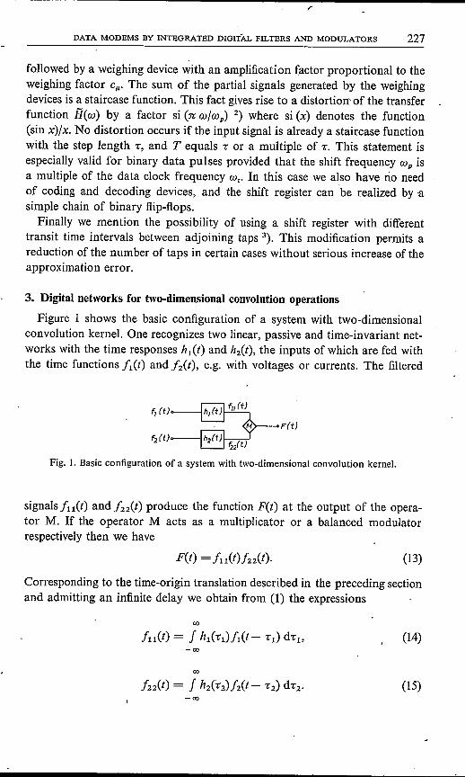
3. Digital networks for two-dimensional convolution operations
Figure 1 shows the basic configuration of a system with two-dimensionalconvolution kernel. One recognizes two linear, passive and time-invariant net-works with the time responses It 1(t) and hz(t), the inputs of which are fed withthe time functions II(t) and 12(t), e.g. with voltages or currents. The filtered
F(t)
Fig. 1. Basic configuration of a system with two-dimensional convolution kernel.
signals lu (t) and f22(t) produce the function F(t) at the output of the opera-tor M. If the operator M acts as a multiplicator or a balanced modulatorrespectively then we have
F(t) = 111(t)/22(t). (13)
Corresponding to the time-origin translation described in the preceding sectionand admitting an infinite delay we obtain from (1) the expressions
00
(1.4)-00
00
(15)-00

228 P. E. LEUTHOLD
Hence from (13) the output function F(t) can be written as follows:
co co
-co -coco co
-eo -ct:)
The introduetion of the two-dimensional kernel
(17)in (16) yields
co co
-00 -co
A physical interpretation of the last double integral shows that the functions11(t) and/it) have to be stored in two delay lines which are tapped in infinites-imal sections. Each tapped partial signalof one line is multiplied byeachtapped partial signalof the other line. The generated products are now weighedin accordance with the two-dimensional kernel h(-c1, -C2)' The integration cor-responds to the summation of all such weighed products.
In the frequency domain expression (18) becomes
(19)
where cfo(w),F1(w) and F2(w) denote the Fourier spectra of the functions F(t),f1(t) and/2(t) respectively, and H1(w) and Hiw) are the transfer functions ofthe networks with the time responses h1(t) and hit) respectively. The sign *stands for the convolution operation. The convolution in (19) corresponds tothe multiplication in (13).The transfer functions H1(W) and Hiw) exist provided that the conditions
00
(20)-00
and00
(21)-00
hold. Consequently the condition00 00
(22)-eo -to

DATA MODEMS BY INTEGRATED DIGITAL FILTERS AND MODULATORS 229
is also valid. Thus the kernel h('r:l> "C2) represents a bowed area over the "Cl> "C2-plane the contours of which vanish for "Cl --+ co and/or "C2 --)- co.
F(t)
Fig. 2. System of paralIel basic configurations.
Figure 2 shows a system of paraIIel basic configurations as depicted in fig. 1.The output signal F(t) can be written as the sum of the outputs of the differentbasic configurations calculated from (16):
-00 -co
-00 -co
-00 -00
This expression assumes the same form as (18) if the two-dimensional kernel
h("Cl> "C2) = hl("Cl) h2("C2) + h3("Cl) h4("C2) + ... + hq("Cl) hq+1("C2) (24)
is introduced. Now the kernel h("Cl, "C2) no longer can be split off in factors ofone variable according to (17). Thus in general it is not possible to reduce theparaIIel system to the basic configuration.It seems to be evident that a physical realization of continuous tapping,
multiplying and weighing is nearlyimpossible. Hence the two delay lines fedwith the input signals fl (t) and fit) have to be tapped at fixed spots. Thetransit time intervals between adjoining taps of the two lines are denoted byTl and T2 respectively. The tapped signals of one line are each multiplied withall tapped signals of the other line by means of a set of modulation elements.The generated products are weighed in accordance with discrete values of the

230 P. E. LEUTHOLD
kernel h(7:1' 7:2), The sum of the weighed products yields the output signal F(t).Corresponding to (3) we. obtain from (18) the finite double sum
m n
F(t) = ~ ~ Tl T2 h(fJ,Tl, vT2)!1(t- fJ,Tl)!it- vT2), (25)JJ=-m v=-n
where 2mTI and 2nT2 are the total delay times of the two lines. From (25) thetwo-dimensional weighing factors can be written as
CJlV = Tl T2 h(fJ,Tl>vT2).
The corresponding relation to (25) in the frequency domain is given by
(26)
In n
JJ.=-m v=-n
If this expression belongs to the basic configuration as shown in fig. 1 theweighing factors cJlV may be split off as follows:
(28)
(29)
(30)
CJl = Tl hl(fJ,Tl),
Cv = T2 h2(vT2) •
Thus (27) can be modified into
In n
Jl=-m v=-n
In accordance with (5) we recognize that cJl and Cv are the coefficients of theFourier series Bl(W) and Biw) approximating the transfer functions Hl(W)and H2(W) defined by the Fourier transforms of the time responses hl(t) andhit). The periodicities of the two Fourier sums are given by wpl = 2n/Tland Wp2 = 2n/T2 respectively. Thus we have
(32)
A comparison of the last expression with 09) shows that such a configurationwith two discretely tapped delay lines has more or less the same properties asa system with continuous tapping. It has only to be borne in mind that the

DATA MODEMS BY INTEGRATED DIGITAL FILTERS AND MODULATORS 231
transfer functions Bl(w) and B2(w) have a periodicity which depends on thechoice of the transit time intervals Tl and T2• The approximation error in theinterval 0 ~ co ~ wpd2 and 0 ::::;;to ::::;;wp2/2 respectively is determined by thenumber 2m + 1 and 2n + 1 of taps. An even number of taps can also beeasily achieved if the weighing factors c21L and C2v are omitted.
:,I I I I I I I I:: ::: : ti' t,
j S21-:---i l_ó-ip------jp;;;-- ' ,~----M:j7------ ,I I I I I JIV, I::: ::: : il:'i i--:---i iPt?------tr---- '~-----4 ..----
F(t)
Fig. 3. Block diagram of a digital network for two-dimensional convolution operations.
Figure 3 shows the block diagram of a digital network for two-dimensionalconvolution operations equipped with -two samplers Al and A2 and twoanalog-digital converters ADC 1 and ADC 2 to process analog input signalsfl (t) and fit). The analog-digital converters are followed by the shift registersSI and S2with the stages ZIL and Z; respectively. Each modulation element MlLv
is fed with the output signals of a stage ZJLand a stage Z; of the two shiftregisters. Due to the fact that these signals are digital the modulation operationcan also be done by digital means. Each modulation element MJLV contains a -decoder. The decoded products are weighed by the factor clLV and the outputsignal F(t) results from a summation of the weighed products. The generatorsPG I and PG 2 produce the pulse trains for the control of the shift registers,analog-digital converters and sampling circuits. There is no condition to bemet by the two shift frequencies Wpl and Wp2' but each shift frequency has tobe chosen equal to the sampling rate Wt! and Wt2 respectively or equal to amultiple of them.Since the application of such networks to analog signal processing is beyond
the scope of.this paper the different methods of quantization, coding and de-coding will not be discussed here. We assume that both input signalsfl(t) and

232 P. E. LEUTHOLD
fit) are binary-pulse trains and Wd and W'2 represents the corresponding clockfrequencies. The shift registers are now simple chains of binary flip-flops con-trolled by the shift frequencies Wpl and Wp2. The modulation elements dege-nerate to simple logic gates (AND, EXCL.-OR, etc.). The weighing devicescan be realized by means of resistors only which are inserted between the out-puts of the modulation elements and a fixed common potential. The con-ductance of the resistors have to be chosen in accordance to the weighingfactor Cpv. Negative weighing factors appear if we use the inverse output of themodulation element. The sum of the currents generated by the resistors yieldsthe desired signal F(t).
For completeness it should be mentioned at this point that the theory out-lined above may be enlarged to more-complicated network structures withmultidimensional convolution kernels 10).
4. The realization of data transmitters by means of digital networks for two-dimensional convolution operations
The basic configuration shown in fig. 1 may be interpreted as a modulatorwhere f11(t) is the band-limited information signal and f22(t) represents thecarrier. When the operator M is a multiplier then we get an amplitude-modu-lated signal F(t) at the output. The network with the time response hl(t) hasto be chosen in such a manner that the binary input data signalfl(t) is band-limited to an upper bound related to the bit rate. The application of meredigital shift registers also requires a binary input carrier signalf2(t) representedby a symmetrical square-wave function. The network with the time responsehit) has now the task to suppress the harmonics of the square-wave carrier.Since the spectrum of the square-wave function consists of a fundamental fre-quency or carrier frequency Wc and a series of harmonics, the suppressingtransfer function H2(w) must have zeros at the positions of the harmonics.For all other frequencies H2(W) may be arbitrary.A finite Fourier series which guarantees an exact position of the zeros results
from the approximation ofthe real part A2(W) and/or the imaginary part Biw)given by
Calculating the time responses of (33) and (34) and using (4) we obtain theFourier coefficients

DATA MODEMS BY INTEGRATED DIGITAL FILTERS AND MODULATORS 233
Wc ( Wc )' Wp22-cos 2nv- , Ivl<-,Wp2 Wp2 2wc
Wc ( Wc) Wp2ä; = -cos 2nv- , lvi=-, (35)
Wp2 Wp2 2wc
0,Wp2
Ivl>-;2wc
\ Wo ( Wo) Wp22- sin 2nv- , Ivl<-,Wp2 Wp2 2wc
Wc ( Wc ) Wp2
b, ~ ( - sin 2nv - , Ivl=-, (36)Wp2 Wp2 2wc
0,Wp2
Ivl>-;2wc
Wp2 is the shift frequency of the carrier shift register. Referring to sec. 2 werecognize that the finite Fourier sum Aiw) with the coefficients a; producesa cosine carrier wavè and the finite Fourier sum B2(W) with the coefficients b;generates a sine carrier wave. Of course the periodic continuation ofthe char-acteristics gives rise to higher-frequency components. One can show, however,that all the harmonics within the interval Wc< W < (Wp2 - wc) are com-pletely suppressed if the space between the pulses of the square-wave carrierequals the pulse length and if the condition
Wp2- = k, k = 2, 3, 4, 5, ...Wc
(37)
holds.For completeness it should be mentioned at this point that the application
of a digital shift register requires an integer ratio of the carrier pulse lengthl"2 = n/wc and the storage time T2 = 2n/wp2 of one register stage. This state-ment is incompatible with (37) if k represents an odd number. In order to solvethis problem we have to use a shift register of double size, the stages of whichproduce a delay of T2/2 only. On the other hand the transit time interval be-tween adjoining taps remains T2•Furthermore the carrier shift register may be replaced by a ring counter 7)
which generates the delayed square-wave carrier. Using register stages withadditional inverse outputs one can reduce their number into half.

234 P. E. LEUTHOLD
4.1. Amplitude modulation (AM)
Figure 4 shows the basic block diagram of the data transmitters which willbe described in the following sections.The binary pulses of the data source Q coincide with a train of synchroniza-
tion pulses produced by the pulse generator PG I of repetition frequency WTI.
,,I I I I I I I II I I I I I I I
" I " I 41is, ~ i jp-jp-------jp;;;-- : ,~---M::r----- ,I I I I I I uv I I ~
:: :.:: : ~:'II: : I: : -----~----: i~~.:::::._.-:~::.:.:....- . .I
" RF(I)
Fig. 4. Basic block diagram of a data transmitter.
The data pulses are fed into the shift register SI which consists of a chain ofbinary flip-flops Zw The shift frequency wp1 is a multiple of the pulse fre-quency Wtl (multiplier VI). The pulse generator PG 2 produces another trainof carrier pulses which are stored in the shift register S2 realized by a chainof binary flip-flops Zv. The shift frequency Wp2 is a multiple of the carrierpulse frequency Wc (multiplier V2). .The output signals ofthe flip-flops ofthe two shift registers supply a matrix W
'defined as a lattice with at least two rows and two c-olumns. The nodes areformed by the crossings of the taps of the two shift registers SI and S2. Eachnode contains a modulation element MlLv which performs a multiplication ofthe output signals of the corresponding flip-flops. In this case all the modula-tion elements Mp.v are logic AND-gates. Their output signals are weighed bymeans of a potentiometer composed of the resistors ruv and R. Addition ofthe weighed voltages on R yields the output signal F(t). With R «ruv theweighing factors are determined by
R(38)

DATA MODEMS BY INTEGRATED DIGITAL FILTERS AND MODULATORS 235
In practice the summation of the currents produced by the resistors ril. can beperformed by an operational amplifier.The transfer function Hl(ro) has to limit the bandwidth of the data signal
/l(t). Approximating an ideallow-pass filter with the cut-off frequency Woweobtain from (11) the Fourier coefficients
(39)
where ropl is the chosen periodicity and si (x) has again the meaning of(sin x)fx. Combining (28), (35) and (39) we get the two-dimensional weighingfactors
(40)
0,
It is now evident why the so-called foldover can be avoided. Contrary to thesystem described in ref. 4 the modulation of the carrier is performed by thealready band-limited data signal. Moreover the carrier is nearly free of har-monics. Obviously these favourable properties result both from a combinationand a local distribution of the digital modulation and filter processes.
4.2. Orthogonal modulationA combination of (28), (36) instead of (35) and (39) yields a set of weighing
factors Y 11. which produces an AM signal orthogonal to the AM signal describedin the preceding section. Hence the orthogonal data transmitter consists of twomatrices with AND-gates and with a respective set of weighing factors ell. andYllv- Each matrix is fed by the taps of a digital shift register which delays thebinary data signal/let) orf2(t) respectively. The taps ofthe carrier shift registerare connected with both the matrices.
4.3. Single-sideband modulation (SSB)
Four different methods are known to generate SSB signals whereofthe phase-shift method 8) and the method of Weaver 9) are well suited to constitute the.basic concept of digital networks for multidimensional convolution operations.
Especially the phase-shift method can be employed to realize an SSB data

236 P. E. LEUTHOLD
transmitter the configuration of which is depicted in fig. 4. If we choose a setof coefficients ell. corresponding to (40) then an ordinary AM signal is pro-duced. Now a second system as shown in fig. 4 has to be used. Combining (34)and the formula
Wo ( WO)(Jll = 2-ci 2'.TCf.J,-,Wp1 Wp1
(41)
which denotes the coefficients of the Fourier series of an ideal low-pass filtercharacteristic with the cut-off frequency Wo and an additional 90° phase shift,we obtain a new set of coefficients 'Yll. in accordance with (40) wheresi (2'.TCf.l wo/wp1) cos (2'.TC'V WC/wp2) is replaced by ei (2'.TCf.l WO/Wp1) sin (2'.TC'V Wc/Wp2)
The abbreviation ei (x) denotes the ratio (1- cos x)/x.This second system generates an orthogonal AM signal modulated by an
approximation of the Hilbert transform of the band-limited information signalf1(t). Now the sum or the difference of the orthogonal AM signals of the twosystems yields the desired SSB signal in the lower or upper sideband respec-tively.From (24) it follows that we have only to use one digital configuration as
depicted in fig. 4 if a new set of weighing factors is defined as the sum or thedifference of the factors ell. and ril. of the two separate systems:
(42)
4.4. Phase modulation (PM)
Binary phase-shift keying and binary AM with suppressed carrier are iden-tical. Thus we can also use the digital configuration of fig. 4, but an additionalsubtraction of the carrier is necessary. This may be easily performed by meansof an additional tapping of the carrier shift register with weighing faètors cor-responding to (35), but with negative sign and half the size, provided that thedata pulses have the standardized amplitudes 0 and 1.One can also show that no additional tapping is required if the AND-gates
of the modulation elements are replaced by modulo-2 adders 10). Hence it isevident that not only a multiplication but also other logic operations may beassigned to the modulation elements. This fact permits a remarkable increasein the versatility of these digital network structures.
4.5. Frequency modulation (FM)
A transmitter with binary frequency-shift keying can be based on the single-sideband system described in sec. 4.3. Thus we have the same configuration asshown in fig. 4, with the exception of an additional OR-gate inserted betweenthe data source Q and the shift register SI' The second input signal ofthe OR-

DATA MODEMS BY INTEGRATED DIGITAL FILTERS AND MODULATORS 237
gate consists of a square-wave function the frequency of which corresponds tothe difference in frequency of the two frequency positions of the binary FMsignal. For a logic 1 of the data signal the digital network generates an outputfrequency equal to the carrier frequency and for a logic 0 the output frequencyis shifted by the difference frequency. Of course the change of logic symbolsoriginates transient frequency components dependent on the slopes of theapproximated frequency characteristics. An additional tapping of the carriershift register for carrier suppression can also be avoided if the modulationelements are equipped with modulo-2 adders.
5. Some genera] remarks on the properties of the digital data transmitter matrix
From the analysis of the equations (35), (36), (39) and (41) which constitutethe expressions (40) and (42) for the two-dimensional weighing factors cjLV werecognize a strong relation to the modulated signals to be produced. Thus, forexample, the coefficients cjLV of (40) result as a product of the sampling valuesof the time response of the low-pass filter and the sampling values of thecarrier wave. In the time domain an AM signal is generated corresponding tothe product of a band-limited information signal and the carrier if harmonicsare neglected. The general validity of these statements can also be shown forthe weighing factors cjLV of the single-sideband transmitter when (42)"is in-terpreted in the same manner.Referring to (26) the coefficients cllV have to be considered as the sampling
values of the two-dimensional kernel h( 7: 1> 7:2) which represents a curved areain the 7:1, 7:2-plane. A study of this area yields some interesting facts aboutsymmetry.Figure 5 shows a map of the kernel h(7:1> 7:2) of a network which produces
i---
Io!-o.,o
I1: \
{ \f r>. ~
_.. \
f r-.\
i() !-0,' I
i
........\i. ···0···.·'/ \ "--'!':-0,2;I <:>i -0,'
o
\.~~:9oI TI
-0,'o
oI
!oi-O.'~._-
Fig. 5. Map of the kernel 1I(-C1' -C2) for the generation of AM signals.

238 P. E. LEUTHOLD
an AM signal, The weighing factors or sampling values cllV = Tl T2 h(~lTl>vT2)
respectively result from (40). The frequency ratios wo//vp1 and WC/wp2 havebeen chosen 1/4 and 1/10. The contour curves are obtained approximativelyby means of an interpolation between the sampling values. Only the interval-mT1 ~?:1 ~ mT1 and -nT2 ~ ?:2 ~ nT2 is depicted with m = n = 5. Thescales for ?:1 and ?:2 are chosen equal; hence the time intervals Tl and T2 havethe same length. We recognize that the area h(?:l' ?:2) is divided into rectangularsegments each ofwhich contains an extremum. Adjacent extrema have oppositesigns. The area has a central symmetry as well as a symmetry relative to theaxes ?:1 and ?:2'
Fig. 6. Map of the kernellz("r:1>"1:2) for the generation of SSB signals (upper sideband).
Figure 6 shows a map of the kernel h(?:l' ?:2) of a network which producesa single-sideband signal. Here the sampling values cllV result from (42) wherethe negative sign has been chosen. This means that the generated signal coversthe upper sideband. The frequency ratios and the time scales are the same asin fig. 5. Contrary to the area in:fig. 5 the rectangular segments have disappeared.The map shows a general structure from the lower left side to the upper right ,side. Adjacent extrema also have opposite signs.The map of the kernel h(?:1' 0"2) of the experimental SSB data transmitter
described in sec. 7 is depicted in fig. 7. The sampling values cllV result from(43) where the positive sign has been chosen. Consequently the lower sidebandappears. The map corresponds to that of fig. 6 but there is a general structurefrom the upper left side to the lower right side. It is therefore interesting tonote that a map structure from down left to up right belongs to an SSB signalin the upper sideband and a map structure from up left to down right belongsto an SSB signal in the lower sideband.
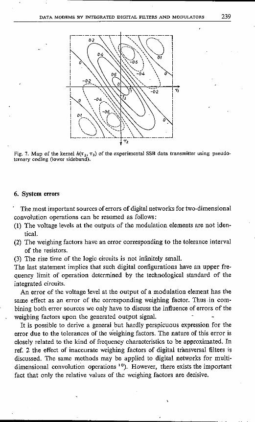
DATA MODEMS BY INTEGRATED DIGITAL FILTERS AND MODULATORS 239
Fig. 7. Map of the kernel h(T1' T2) of the experimental SSB data transmitter using pseudo-ternary coding (lower sideband).
6. System errors
. The most important sources of errors of digital networks for two-dimensionalconvolution operations can be resumed as follows:(1) The voltage levels at the outputs of the modulation elements are not iden-
tical.(2) The weighing factors have an error corresponding to the tolerance interval
of the resistors.(3) The rise time of the logic circuits is not infinitely small.The last statement implies that such digital configurations have an upper fre-quency limit of operation determined by the technological standard of theintegrated circuits.An error of the voltage level at the output of a modulation element has the
same effect as an error of the corresponding weighing factor. Thus in com-bining both error sources we only have to discuss the influence of errors of theweighing factors upon the generated output signal.It is possible to derive a general but hardly perspicuous expression for the
error due to the tolerances of the weighing factors. The nature of this error isclosely related to the kind of frequency characteristics to be approximated. Inref. 2 the effect of inaccurate weighing factors of digital transversal filters isdiscussed. The same methods may be applied to digital networks for multi-dimensional convolution operations 10). However, there exists the importantfact that only the relative values of the weighing factors are decisive.

240 P. E. LEUTHOLD
7. An experimental SSB data transmitter
In order to confirm the theory developed in the preceding chapters an ex-perimental SSB data transmitter has been realized based on the principle de-scribed in sec. 4.3. The corresponding block diagram is shown in fig. 4. Usingpseudo-ternary coding of the binary data signal we obtain the weighing factorsCjlV in accordance with (42):
0,
(43)
A detailed discussion of the frequency characteristics to be approximated isgiven in ref. 11.The SSB transmitter intended for data transmission over telephone channels
with 1200 bit/s has the following specifications:
carrier frequency:WcIc = -= 2·1 kHz,2:n
data clock frequency:Wtl
fel = - = 1·2kHz,2:n
cut-off frequency:Wo
fo = -= 0·6 kHz,2:n
shift frequency:Wpl .
fpl = - = 2·4 kHz,2:n
shift frequency:. Wp2fp2 = - = 21 kHz.2:n
Using the plus sign in (43) we get a SSB signal in the lower sideband between1·5 kHz and 2·1 kHz.

DATA MODEMS BY INTEGRATED DIGITAL FILTERS AND MODULATORS 241
The two digital shift registers SJ and S2 (fig. 4) are composed each of 11stages only. Hence a quadratic matrix W with 11 X 11 = 121 nodes results.The currents produced by the AND-gates of the modulation elements Mlly
connected to the weighing resistors rlly are summed up by means of an opera-tional amplifier which generates the SSB output voltage.
Fig. 8. Output signa! of the SSB transmitter. Above: unrnodulated carrier, below: SSB signal.
Figure 8 shows the unmodulated carrier and the SSB signal at the output ofthe transmitter. Naturally these signals appear in the form of staircase voltages.Since in general the ratio wjwtJ is not an integer the step length changes atcertain moments. The spectrum of the SSB signal shown in fig. 8 is given infig. 9. Since the modulating signal consists of a periodically repeated data pulsetrain of 16 bits the space between adjoining spectrallines is 1/16 of the dataclock frequency Irt = 1·2 kHz, that is 75 Hz. One recognizes the lower side-band and the suppressed upper sideband. The magnitude of suppression liesin the range of 25 dB. The higher-order spectra on the right side and on theleft side of the lower sideband results from the periodicity of the low-passcharacteristic which limits the data signal band. Contrary to the SSB trans-mitter described in ref. 11 we have ony little suppression of the carrier. Thisfollows from the poor approximation of the 90° wideband phase-shifter char-acteristic by means of finite Fourier sums at low frequencies and from theconstraint to use direct-current coupling.
With a total tolerance of 1·5% for the weighing factors measurements of thefrequency components in the lower sideband reveal that the influence of fold-over produces an error of less than 2%.

242 P. E. LEUTHOLD
Fig. 9. Frequency spectrum of the SSB signal produced by the periodically repeated datapulse train" 1011101001000010". Scale: centre frequency 2'1 kHz, origin of the frequencyabscissa marked by the single peak on the left side.
Clearly the suppression of the upper sideband and of the carrier can beimproved if we enlarge the number of stages of the shift register S I (fig. 4).For instance an increase of 50% yields an improvement of about 10 dB J1).Also, the space between the signalling band used and the higher-order spectramay be increased if we enlarge the shift frequency Wp1' Obviously the corre-sponding reduction of the approximation quality of the given low-pass char-acteristic has also to be compensated by an increase of the number of shift-register stages.
8. Conclusions
It has been shown that digital networks for two-dimensional convolutionoperations offer the possibility to realize parts of communication systems.Such networks lend themselves also to applications in the field of measuringtechniques and of control systems.
An inherent property of these digital networks is a homogeneous structurecomposed of only three elements: storage elements (flip-flops), modulationelements (logic gates) and weighing elements (resistors). From this it followsthat large-scale integration of the entire networks can be achieved.
The relation between the input signals and the output signal is simply givenby the type of logic gates used as modulation elements and by the magnitudeof the weighing factors. The modulation elements mayalso drive more than

DATA MODEMS BY INTEGRATED DIGITAL FILTERS AND MODULATORS 243
one set of weighing elements. In this case various systems can be incorporatedin a single digital network. \Due to the possibility of using convolution integrals the theory remains
relatively simple and transparent. The weighing factors are determined by'discrete values of the two-dimensional kernel functions.Various applications of digital networks for two-dimensional convolution
operations in data-transmission systems are discussed. Data transmitters real-ized in this way are well suited for large-scale integration. They are nearly freeof modulation distortion particularly caused by harmonic components andfoldover. Furthermore they permit a change of the data clock frequency and/orthe carrier frequency over a wide frequency range without any modificationof the digital network employed.Data receivers can also be constructed from digital networks for two- or
multidimensional convolution operations when the analog-modulated signal atthe channel exit is first processed by means of an analog-digital converter.
. Acknowledgement
The author wishes to acknowledge the support and stimulation given to hiswork by Prof. Dr F. E. Borgnis, Director of the Institute of High FrequencyElectronics at the Federal Institute of Technology in Zurich. Special apprecia-tion is also expressed to W. Widmer who built the experimental data trans-mitter described above with skill and perseverance.
Fede~alInstitute of Technology Zürich, July 1971
REFERENCES1) H. E. Kallmann, Proc. IRE 2S, 302-310, 1940.2) P. E. Leuthold, Philips Res. Repts Suppl. 1967, No. 5.3) H. B. Voelcker, IEEE Trans. Comm. Techn. Com-16, 81-93, 1968.4) P. J. van Genven and P. van der Wurf, Trans. Comm. Techn. Com-lS, 214-222,1970.5) W. R. Bennett and J. R. Davey, Data transmission, McGraw-Hill, New York, 1965,
p.134.6) E. R. Hafner and P. E. Leuthold, Proc. IEEE 57,2114-2122, 1969.7) J. Millman and H. Taub, Pulse, digital, and switching waveforms, McGraw-HiII, New
York, 1965, pp. 693-698.8) n, E. Norgaard, Proc. IRE 44,1718-1735,1956.9) D. K. Weaver, Proc. IRE 44, 1703-1705,1956.
10) P. E. Leuthold, Digitale Netzwerkstrukturen zur Durchführung von Faltungsoperatio-nen mit mehrdimensionalen Kernen, Habilitationsschrift, Institut für Hochfrequenz-technik, Eidgenössische Technische Hochschule Zürich, Februar 1970.
11) P. E. Leu thold and F. Tisi, Archiv el. Uebertr. 21, 354-362, 1967.