A New CMOS Topology for Low-Voltage Null Convention...
8
A New CMOS Topology for Low Voltage Null Convention Logic Gates Design Matheus Trevisan Moreira, Michel Evandro Arendt, Ricardo Aquino Guazzelli, Ney Laert Vilar Calazans GAPH – FACIN – Potifical Catholic University of Rio Grande do Sul Porto Alegre, Brazil {matheus.moreira, ney.calazans}@pucrs.br, {michel.arendt, ricardo.guazzelli}@acad.pucrs.br Abstract—This paper proposes a new transistor topology to design gates required by Null Convention Logic for low voltage operation. The new topology enables implement all functionalities required by this design style. Extensive simulation results con- ducted in a 65 nm CMOS technology allow comparing the new topology to popular static and semi-static ones and indicate that the former presents better speed, energy and leakage trade-offs for different voltage levels, demonstrating the suitability of the new topology for low voltage applications. Drawbacks are an area of 4 minimum size transistors and reduced robustness against soft errors, when operating at non-minimum voltages. Keywords—Null Convention Logic, static, low-power. I. INTRODUCTION Asynchronous or clockless circuit design can cope better with inherent problems of current technologies that make syn- chronous design over constrained, like susceptibility to PVT variations and excessive power dissipation in clock trees. Albe- it asynchronous circuits can be implemented using many dif- ferent templates, the quasi-delay-insensitive (QDI) [1] template is attractive for several reasons, but especially because it allows wire and gate delays to be ignored, given that the isochronic fork [2] delay assumption is respected. This allows QDI cir- cuits to better accommodate delay discrepancies caused by PVT variations, making them more robust than circuits based on templates that rely on complex timing assumptions. Also, with QDI, design complexity can be considerably reduced, facilitating timing closure and analysis. The definition of a specific QDI template requires the choice of a handshake protocol and a delay-insensitive (DI) data encoding. According to Martin and Nyström [3], the 4- phase handshaking protocol coupled to either 1-of-2 or 1-of-4 codes comprises almost the entirety of options in practical QDI design. For such templates, various logic styles support sequen- tial and combinational logic implementations. Of the styles proposed to date, the Null Convention Logic (NCL) [4] is one that enables power-, area- and speed-efficient design [5]-[11] based on standard cells. In fact, NCL has been successfully employed in the design of many fabricated chips, as discussed in [12]. Also, several design flows have been proposed to date to help automating NCL design, as described in [12]-[15]. In this paper we propose a new CMOS topology for imple- menting gates required by NCL design at the standard-cell lev- el. The topology is compared to the classic static and semi- static topologies in the following aspects: Post-layout extraction input capacitance and internal para- sitics; Area, speed and power tradeoffs; Vulnerability to PVT variations; Applicability to voltage scaling applications; Robustness against single event effects. For the sake of comparison, 27 case study gates were de- signed to layout level targeting a 65nm bulk CMOS technology from STMicroelectronics. These gates employed 3 different NCL functionalities implemented using 3 different topologies (static, semi-static and the proposed one) for 3 different driving strengths. Results indicate that the proposed topology is suited for voltage scaling applications and presents better speed, ener- gy and power tradeoffs for the increased silicon area cost. This cost is fixed: 4 minimum sized transistors per gate. Also, the proposed topology is generally more robust against PVT varia- tions and presents lower input and parasitic capacitances. II. NULL CONVENTION LOGIC Theseus Logic, Inc. [4] proposed NCL, a logic that has been employed to implement QDI asynchronous systems on silicon. NCL is an alternative to other design styles like delay insensi- tive minterm synthesis (DIMS) [16] and was applied to cope with power problems [5]-[7], to design high speed circuits [8] [9] and to fault tolerant schemes [10] [11], as well as other ap- plications such as ternary logic [17]. One of its advantages is to enable power-, area- and speed-efficient QDI design with a standard-cell-based approach, while other asynchronous tem- plates require recourse to full-custom approaches. NCL gates are sometimes called threshold gates, but this is imprecise. In fact, NCL gates couple a threshold function [18] with positive integer weights assigned to inputs to the use of a hysteresis mechanism. This is required to support DI circuit design using 1-of-n data encoding. Figure 1 shows a generic NCL gate symbol. I 1 I 2 I 3 I N ... MWw1..wn Q Figure 1 – Basic NCL gate symbol. In NCL gates N is the number of gate inputs, M is the gate threshold or a threshold function, and each input has a weight (wi). Wherever no weight is specified, weight 1 is assumed. Weights come after the W specifier. The output switches to 0 when all N inputs are 0 and to 1 when the sum of weights for 2014 20th IEEE International Symposium on Asynchronous Circuits and Systems 1522-8681/14 $31.00 © 2014 IEEE DOI 10.1109/ASYNC.2014.20 93
Transcript of A New CMOS Topology for Low-Voltage Null Convention...
A New CMOS Topology for Low Voltage Null Convention Logic Gates Design
Matheus Trevisan Moreira, Michel Evandro Arendt, Ricardo Aquino Guazzelli, Ney Laert Vilar Calazans GAPH – FACIN – Potifical Catholic University of Rio Grande do Sul
Porto Alegre, Brazil {matheus.moreira, ney.calazans}@pucrs.br, {michel.arendt, ricardo.guazzelli}@acad.pucrs.br
Abstract—This paper proposes a new transistor topology to
design gates required by Null Convention Logic for low voltage operation. The new topology enables implement all functionalities required by this design style. Extensive simulation results con-ducted in a 65 nm CMOS technology allow comparing the new topology to popular static and semi-static ones and indicate that the former presents better speed, energy and leakage trade-offs for different voltage levels, demonstrating the suitability of the new topology for low voltage applications. Drawbacks are an area of 4 minimum size transistors and reduced robustness against soft errors, when operating at non-minimum voltages.
Keywords—Null Convention Logic, static, low-power.
I. INTRODUCTION Asynchronous or clockless circuit design can cope better
with inherent problems of current technologies that make syn-chronous design over constrained, like susceptibility to PVT variations and excessive power dissipation in clock trees. Albe-it asynchronous circuits can be implemented using many dif-ferent templates, the quasi-delay-insensitive (QDI) [1] template is attractive for several reasons, but especially because it allows wire and gate delays to be ignored, given that the isochronic fork [2] delay assumption is respected. This allows QDI cir-cuits to better accommodate delay discrepancies caused by PVT variations, making them more robust than circuits based on templates that rely on complex timing assumptions. Also, with QDI, design complexity can be considerably reduced, facilitating timing closure and analysis.
The definition of a specific QDI template requires the choice of a handshake protocol and a delay-insensitive (DI) data encoding. According to Martin and Nyström [3], the 4-phase handshaking protocol coupled to either 1-of-2 or 1-of-4 codes comprises almost the entirety of options in practical QDI design. For such templates, various logic styles support sequen-tial and combinational logic implementations. Of the styles proposed to date, the Null Convention Logic (NCL) [4] is one that enables power-, area- and speed-efficient design [5]-[11] based on standard cells. In fact, NCL has been successfully employed in the design of many fabricated chips, as discussed in [12]. Also, several design flows have been proposed to date to help automating NCL design, as described in [12]-[15].
In this paper we propose a new CMOS topology for imple-menting gates required by NCL design at the standard-cell lev-el. The topology is compared to the classic static and semi-static topologies in the following aspects:
� Post-layout extraction input capacitance and internal para-sitics;
� Area, speed and power tradeoffs; � Vulnerability to PVT variations; � Applicability to voltage scaling applications; � Robustness against single event effects.
For the sake of comparison, 27 case study gates were de-signed to layout level targeting a 65nm bulk CMOS technology from STMicroelectronics. These gates employed 3 different NCL functionalities implemented using 3 different topologies (static, semi-static and the proposed one) for 3 different driving strengths. Results indicate that the proposed topology is suited for voltage scaling applications and presents better speed, ener-gy and power tradeoffs for the increased silicon area cost. This cost is fixed: 4 minimum sized transistors per gate. Also, the proposed topology is generally more robust against PVT varia-tions and presents lower input and parasitic capacitances.
II. NULL CONVENTION LOGIC Theseus Logic, Inc. [4] proposed NCL, a logic that has been
employed to implement QDI asynchronous systems on silicon. NCL is an alternative to other design styles like delay insensi-tive minterm synthesis (DIMS) [16] and was applied to cope with power problems [5]-[7], to design high speed circuits [8] [9] and to fault tolerant schemes [10] [11], as well as other ap-plications such as ternary logic [17]. One of its advantages is to enable power-, area- and speed-efficient QDI design with a standard-cell-based approach, while other asynchronous tem-plates require recourse to full-custom approaches. NCL gates are sometimes called threshold gates, but this is imprecise. In fact, NCL gates couple a threshold function [18] with positive integer weights assigned to inputs to the use of a hysteresis mechanism. This is required to support DI circuit design using 1-of-n data encoding.
Figure 1 shows a generic NCL gate symbol. I1I2I3IN
...MWw1..wn
Q
Figure 1 – Basic NCL gate symbol.
In NCL gates N is the number of gate inputs, M is the gate threshold or a threshold function, and each input has a weight (wi). Wherever no weight is specified, weight 1 is assumed. Weights come after the W specifier. The output switches to 0 when all N inputs are 0 and to 1 when the sum of weights for
2014 20th IEEE International Symposium on Asynchronous Circuits and Systems
1522-8681/14 $31.00 © 2014 IEEE
DOI 10.1109/ASYNC.2014.20
93

inputs at 1 reaches threshold M or satisfies the threshold func-tion. Otherwise, the previous output value is maintained.
There are different manners of implementing NCL gates as standard-cells. Some rely on the usage of differential logic, as discussed in [19] and [20]. However, this requires structural modifications in the design and is not compatible with state-of-the-art methods and tools for NCL design automation. Others rely on the usage of multi-threshold CMOS technologies, as discussed in [21]. However, these also require the availability of specific technologies and are not directly compatible with methods and tools proposed to date. Therefore we do not con-sider differential or multi-threshold topologies in this work. We also discard the topology proposed in [22] as it does not present a general schematic and requires gate specific designs.
In fact, this work considers the static and semi-static topol-ogies [23], which are most referred in literature and have been successfully fabricated on silicon. Note that we also discarded dynamic topologies [23] as these are not suited to QDI design. In the classic semi-static topology, presented in Figure 2 (a), the reset and set functions correspond to pull-up (RESET) and pull-down (SET) networks, followed by an output inverter. RESET detects when all inputs are 0, corresponding to a series of N PMOS transistors. Note that the output Q is then inverted by output inverter composed by P0 and N0. SET depends on the gate threshold M. Also, to ensure delay insensitivity, the gate keeps its output value when neither RESET nor SET func-tions are true. Since these are not complementary, the static gate requires a feedback inverter, composed by P1 and N1. Note that this inverter is typically minimum size, as it is not required for output switching, being used just for keeping the output stable (a memory effect). In fact, using a minimum size inverter allows reducing interference during gate switching.
The static topology, presented in Figure 2 (b) is similar to the semi-static one. However, its feedback inverter is con-trolled by pull-up (HOLD0) and pull-down (HOLD1) net-works. The former is the complement network of SET and the latter is the complement network of RESET. This allows avoid-ing that the feedback inverter interferes during output switch-ing. Note that for both static and semi-static topologies, the output inverter transistors are sized to be able to drive the out-put load. Transistors of the RESET and SET functions are di-mensioned to drive the equivalent input capacitance of the out-put inverter. All remaining transistors can be minimum size.
It is common knowledge that static topologies are typically more power efficient, while semi-static ones are more area efficient [24] [25]. Also, according to Moreira and Calazans [26] and Bastos et al. [27], the static topology is more suited to voltage scaling applications, while the semi-static one is more robust to single event effects. These works explored static and semi-static C-Element topologies that are compatible with NCL gates, since basic C-Elements are the special case of NCL gates where threshold M is equal to the number of inputs N, with inputs weights all equal to 1.
III. THE PROPOSED TOPOLOGY This work proposes the alternative NCL topology displayed
in Figure 2 (c). In it, output Q switches to 1 or 0, according to the set and reset transistors P0 and N0, respectively. Dimen-
sioning of these follows a process similar to that of the output inverter for the topologies previously mentioned. The same RESET and SET networks control these transistors. However, the latter are respectively connected to their complements HOLD1 and HOLD0 networks. Accordingly, the P0 and N0 driving transistors are both turned off by a hold state input combination. This state uses transistors P1 to P3 and N1 to N3 to maintain the output stable. All these are minimum sized and the mechanism employs a loop of two inverters (P1-N1 and P3-N3), where the driving inverter (P3-N3) is controlled by HOLD1/RESET or by HOLD0/SET (through P2 and N2). Note that HOLD0 and HOLD1 transistors are also minimum size and transistors used for SET and RESET are dimensioned for driv-ing P0 and N0 input capacitance loads. Also, since C-elements are special NCL gates the new scheme is also a new topology for C-elements.
VDD
QRE
SE
TS
ET
P0
N0
P1
N1
VDD
Q
RESET
HOLD 1
P0
P2
P3 P1
N0
N2
N3 N1VDD
HOLD 0
SET
VDD
(a) VDD
QRES
ETSE
T
HOLD 1
HOLD 0
P0
N0
P1
N1
(b) (c)
Figure 2 – NCL topologies: (a) semi-static; (b) static; (c) proposed.
The new scheme guarantees that P0 and N0 will never be on simultaneously, since the RESET network is on only when all inputs are 0, while SET requires that at least one input be 1. Practical SET functions require at least 2 inputs to be 1. This renders the proposed topology even more interesting, because momentary shorts present in the output inverter of the static topology are avoided. In fact, before making either P0 or N0 on, both transistors are always turned off, because as soon as SET and RESET are off, their complements HOLD0 or HOLD1 will be on, and a minimum of two inputs are required to switch from an on SET network to an on RESET network and vice-versa. Also, because input capacitances of P0 and N0 are de-coupled, contrary to what happens in the classical static and semi-static topologies, SET and RESET networks need to drive smaller capacitances to switch the output. In this way, better power and delay tradeoffs are expected as characteristics of the new topology.
IV. EXPERIMENTS AND DISCUSSION
A. Gates Design In order to compare the discussed topologies, 3 different
NCL functionalities were implemented until the layout level
94
for 3 different driving strengths (X2, X7 and X13) for the stat-ic, semi-static and proposed topologies. This produced a total of 3*3*3=27 case study gates. The target technology was the STMicroelectronics 65nm bulk CMOS and gate design fol-lowed the flow proposed by the authors in [28]. This flow re-lies on the use of specially designed design automation tools as well as on the Cadence Framework and Mentor Calibre for layout verification and extraction. Selected functionalities were1: 2-of-2 (M=2, N=2 and weights=1 1); AO2-of-4 (M=AndOr, N=4 and weights=1 1 1 1); 3W22-of-4 (M=3, N=4 and weights=2 2 1 1). This choice allows evaluating trade-offs of topologies for low (2-of-2), medium (AndOr2-of-4) and high (3W22-of-4) complexity gates. Also, in the authors expe-rience these functionalities are widely used in NCL design. After layout extraction, analog simulation allows evaluating the case study gates. All results presented herein are based on worst case RC parasitics extraction.
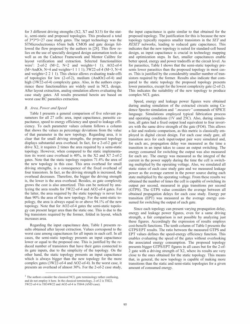
B. Area, Power and Speed Table I presents a general comparison of five relevant pa-
rameters for all 27 cells: area, input capacitance, parasitic ca-pacitance, speed to energy efficiency and speed to leakage effi-ciency. To each parameter values column follows a column that shows the values as percentage deviations from the value of that parameter in the new topology. Regarding area, it is clear that for small driving strengths, the proposed topology displays substantial area overhead. In fact, for a 2-of-2 gate of drive X2, it requires 2 times the area required by a semi-static topology. However, when compared to the static implementa-tion its worst case overhead is 40%, in the X2 and X7 2-of-2 gates. Note that the static topology requires 71.4% the area of the new topology in this case. This area overhead for small driving strengths, is a consequence of the fixed overhead of four transistors. In fact, as the driving strength is increased, the overhead decreases. Therefore, the bigger the driving strength is, the lower is the area overhead. Besides, as gate complexity grows the cost is also amortized. This can be noticed by ana-lyzing the area results for 3W22-of-4 and AO2-of-4 gates. For the latter, the area required by the static topology is never less than 90% the area of the new topology. For the semi-static to-pology, the area is always equal to or above 94.1% of the new topology. Note that for AO2-of-4 gates the semi-static topolo-gy can present larger area than the static one. This is due to the big transistors required by the former, folded in layout, which increases area.
Regarding the input capacitance data, Table I presents re-sults obtained after layout extraction. Values correspond to the worst case among capacitances for all inputs in each cell. In all cases, the semi-static topology presents an input capacitance lower or equal to the proposed one. This is justified by the re-duced number of transistors that have their gates connected to its gate inputs, due to the simplicity of the topology. On the other hand, the static topology presents an input capacitance which is always bigger than the new topology for the more complex gates (3W22-of-4 and AO2-of-4). In the worst case, it presents an overhead of almost 30%. For the 2-of-2 case study,
1 The authors consider the classical NCL gate terminology rather confusing, and do not employ it here. In the classical terminology, 2-of-2 is TH22, 3W22-of-4 is TH34W22 and AO2-of-4 is TH44 (AND case).
the input capacitance is quite similar to that obtained for the proposed topology. The justification for this is because the new topology typically requires smaller transistors in the SET and RESET networks, leading to reduced gate capacitance. This indicates that the new topology is suited for standard-cell based design, as input capacitance is crucial in technology mapping and optimization steps. In fact, smaller capacitances enable better speed, energy and power tradeoffs at the circuit level. As for parasitics, Table I shows that the semi-static topology pre-sents lower parasitics than the proposed topology in most cas-es. This is justified by the considerably smaller number of tran-sistors required by the former. Results also indicate that com-pared to the static topology the proposed topology presents lower parasitics, except for the lowest complexity gate (2-of-2). This indicates the suitability of the new topology to produce complex NCL gates.
Speed, energy and leakage power figures were obtained during analog simulation of the extracted circuits using Ca-dence Spectre simulation and “.measure” commands of SPICE language. Simulations employed typical fabrication process and operating conditions (1V and 25C). Also, during simula-tion, all gates had a fixed output load equivalent to four invert-ers with the same drive strength of the gate (FO4). This allows a fair and realistic comparison, as this metric is classically em-ployed in digital circuit design. For each case study gate, all transition arcs for each input/output pair were simulated and, for each arc, propagation delay was measured as the time a transition in an input takes to cause an output switching. The energy consumed for switching the output was also measured for each arc. The energy was measured as the integral of the current in the power supply during the time the cell is switch-ing multiplied by the operating voltage. Also, we simulated all static states of each case study gate and we measured leakage power as the average current in the power source during each state multiplied by the operating voltage. From these results we obtained the number of times the cell is capable of switching its output per second, measured in giga transitions per second (GTPS). The GTPS value considers the average between all obtained propagation delays for each case study. Energy per transition (EPT) was measured as the average energy con-sumed for switching the output of each gate.
Since each topology can present varying propagation delay, energy and leakage power figures, even for a same driving strength, a fair comparison is not possible by analyzing just these figures. Accordingly the expression of results employs cost-benefit functions. The tenth column of Table I presents the GTPS/EPT results. The ratio between the measured GTPS and EPT values defines the speed-energy efficiency function. This enables evaluating the speed of the gates without overlooking the associated energy consumption. The proposed topology presents bigger GTPS/EPT figures in all cases but for the 2-of-2 gate with a driving strength of X2, where its results are very close to the ones obtained for the static topology. This means that, in general, the new topology is capable of making more transitions than the static and semi-static topologies for a given amount of consumed energy.
95

Table I – Area, input and parasitic capacitances, speed-energy and speed-leakage tradeoffs for the case study gates. All-bold columns are rela-tive comparisons between the proposed topology and the others.
NCL Function Drive Topology Area
(µm²) % of Pro-
posed Input
Cap. (fF) % of Pro-
posed Parasitic Cap. (fF)
% of Pro-
posed GTPS /
EPT % of Pro-
posed
GTPS / Avg. Leak-
age
% of Pro-
posed 2-
of-2
X2 Proposed 7.28 100.0 0.61 100.0 3.760 100.0 5.74 100.0 0.12 100.0 Static 5.2 71.4 0.6 98.4 3.084 82.0 5.87 102.3 0.13 108.3 Semi Static 3.64 50.0 0.36 59.0 1.766 47.0 3.35 58.4 0.07 58.3
X7 Proposed 7.28 100.0 0.62 100.0 3.662 100.0 3.82 100.0 0.08 100.0 Static 5.2 71.4 0.66 106.5 3.40 92.8 2.86 74.9 0.06 75.0 Semi Static 3.64 50.0 0.36 58.1 1.966 53.7 2.46 64.4 0.05 62.5
X13 Proposed 8.32 100.0 0.78 100.0 4.98 100.0 2.19 100.0 0.05 100.0 Static 6.76 81.3 0.69 88.5 3.821 76.7 1.52 69.4 0.03 60.0 Semi Static 5.72 68.8 0.78 100.0 4.32 86.7 1.64 74.9 0.04 80.0
3W22
-of-4
X2 Proposed 11.44 100.0 1.2 100.0 7.190 100.0 3.36 100.0 0.31 100.0 Static 9.36 81.8 1.34 111.7 7.986 111.1 3.33 99.1 0.47 151.6 Semi Static 8.84 77.3 0.77 64.2 5.77 80.3 1.58 47.0 0.27 87.1
X7 Proposed 11.44 100.0 1.18 100.0 7.723 100.0 2.30 100.0 0.25 100.0 Static 9.36 81.8 1.53 129.7 8.44 109.3 1.80 78.3 0.28 112.0 Semi Static 8.84 77.3 0.77 65.3 6 77.7 1.32 57.4 0.21 84.0
X13 Proposed 13 100.0 0.93 100.0 8.657 100.0 1.36 100.0 0.17 100.0 Static 10.92 84.0 1.2 129.0 8.7 100.5 0.99 72.8 0.16 94.1 Semi Static 9.36 72.0 0.81 87.1 6.544 75.6 0.88 64.7 0.14 82.4
AO
2-of
-4
X2 Proposed 8.84 100.0 0.77 100.0 5.754 100.0 3.43 100.0 0.35 100.0 Static 8.32 94.1 0.94 122.1 6.344 110.3 3.21 93.6 0.49 140.0 Semi Static 8.84 100.0 0.64 83.1 4.83 83.9 1.37 39.9 0.29 82.9
X7 Proposed 9.36 100.0 0.77 100.0 5.938 100.0 2.56 100.0 0.30 100.0 Static 8.84 94.4 0.91 118.2 6.24 105.1 1.68 65.6 0.28 93.3 Semi Static 8.84 94.4 0.64 83.1 4.83 81.3 1.24 48.4 0.23 76.7
X13 Proposed 10.4 100.0 0.76 100.0 6.73 100.0 1.61 100.0 0.20 100.0 Static 9.36 90.0 0.97 127.6 6.938 103.1 0.94 58.4 0.16 80.0 Semi Static 9.88 95.0 0.67 88.2 7.27 108.0 0.89 55.3 0.16 80.0
Note that the bigger the driving strength is the bigger is the gain in delay-energy efficiency of the proposed topology. In the best case, an improvement of over 150% is observed when compared to the static topology. E.g. for the AO2-of-4 gate, the static topology has a value of GTPS/EPT that is just 39.9% of the new topology value. This is justified by the fact that the new topology has typically lower capacitances to drive when switching the output. Note that in this topology (refer to Figure 2(c)) the gate capacitances of the PMOS and NMOS transistors of the output inverter (P0 and N0) are decoupled. In this way, the proposed topology is suited for energy efficient applica-tions. Also, the proposed topology is well suited for standard-cell-based design, as its speed-energy efficiency does not decay as in the static and semi-static topologies as driving strength increases. This allows design optimizations to take place with-out compromising low power operation.
Table I also shows speed-leakage efficiency results. GTPS/Average Leakage was measured as the obtained GTPS for each gate divided by the average leakage power. This cre-ates a cost function to evaluate speed-leakage tradeoffs and enables analyzing the speed of the gates without overlooking leakage power. In this case, improvements were not as substan-tial as in delay-energy tradeoffs. In fact, for X2 gates, our to-pology presented worse GTPS/Average Leakage tradeoffs in all cases. However, as the driving strength increases, our topol-ogy proves to be more efficient in terms of the speed-leakage power tradeoff. In the best case, improvements were of more than 70%. This corroborates the previous results that indicate the suitability of the topology for cell-based design.
C. Process, Voltage and Temperature Variations Another desirable feature for contemporary integrated cir-
cuits is increased tolerance to process, voltage and temperature (PVT) variations. In fact, process variations are a critical prob-lem in current technologies. A second set of experiments ena-bled to measure the variability in the observed performance figures for the case study gates while varying operating volt-age, temperature and process fabrication parameters. Note that, because leakage variations were not significant and there were little discrepancies between the analyzed gates, the paper pre-sent only results obtained for propagation delay and energy per transition.
Firstly, we submitted the gates to variations in operating voltage and temperature. We simulated these for a range from 90% to 110% of the nominal values (1V and 25C) in steps of 1%, combining all possible values. This means 21 distinct volt-ages and temperatures that combined lead to 21*21=441 simu-lation scenarios for each gate. Figure 3 shows the variations observed in measured energy per transition. In the Figure, case study gates are distributed along the horizontal axis. A PR pre-fix indicates the gate employs the proposed topology; an ST prefix indicates it employs the static topology and an SS prefix indicates it employs the semi-static topology. Also, 22 stands for a 2-of-2 gate, 3W22 is a 3W22-of-4 gate and AO24 is an AO2-of-4 gate. Gate names were abbreviated to allow a more compact representation in the charts. In these, variations can be either positive or negative and they are measured from the base value obtained for nominal voltage and temperature, represent-ed by the 0 value in the vertical axis in the charts. Note that in
96

most cases the proposed topology presents smaller amplitude in energy per transition variations, when compared to the other topologies. Also, as driving strength is increased, susceptibility to voltage and temperature variations is worsened in all topolo-gies. However, for the proposed topology, the increase is not as substantial as in for the static and semi-static topologies.
Concerning variations in propagation delay, Figure 4 shows that all topologies present similar susceptibility to voltage and temperature variations. However, for the biggest simulated driving strength, the proposed topology always presents small-er variations. In this way, charts of Figure 3 and Figure 4 con-firm the suitability of the proposed topology for standard-cell-based design.
Figure 3 – Energy variation distribution for varying operating voltage
and temperature.2
Figure 4 – Propagation delay variation distribution for varying oper-
ating voltage and temperature.
A second set of simulations allowed evaluating the effect of process variations in gate performance figures. To do this, we proceeded to a process and mismatch Monte Carlo analysis with 5000 samples and measured energy per transition and average propagation delay for each simulated scenario. The charts in Figure 5 and Figure 6 summarize the results. Figure 5 shows the proposed topology presents smaller variations in energy per transition than the other topologies for X7 and X13 driving strengths. For X2, the results observed are comparable to those of the static topology. As for the observed propagation delay variations, the proposed topology presents values compa-rable to the ones observed for the static topology in most cases. Note that PVT variations are more significant in the semi-static topology. This is expected, as this topology relies on the usage
2 Note that, for Figures 3-6, data were divided into 10 sets (5 positive and 5 negative). Each color represents a quintile of positive sets (in red) and nega-tive sets (in blue), where darker colors represent lower quintiles and brighter colors represent upper quintiles.
of a weak inverter for maintaining the output stable, which imposes a resistance when switching the output, while the other topologies employ a more sophisticated and expensive mecha-nism (see Figure 2). Also, in general, the proposed topology is the most robust against PVT variations.
Figure 5 – Energy variation distribution observed from Monte Carlo
analysis.
Figure 6 – Propagation delay variation distribution observed from
Monte Carlo analysis.
D. Voltage Scaling Another very important aspect for contemporary technolo-
gies is the ability to operate at voltage levels lower than the nominal. In fact, according to Hanson et al. [29], voltage scal-ing is the most effective solution to cope with increasing power constraints. Accordingly, we performed a set of experiments to evaluate the impact of voltage scaling in the case study gates. The first experiment detected the minimum voltages that can be applied to each gate without interfering in their correct be-havior. The experiment investigated scenarios for varying tem-peratures and a fixed fan-out of four (FO4) output load. Mini-mum voltages were estimated by simulating all transition arcs and static states of each gate for each temperature/voltage sce-nario. When at least one arc does not generate the correct out-put or a static state is not able to maintain correct functionality, the scenario is defined as not functional. Also, the signals gen-erated must have voltages in well defined regions, for logic ‘1’ (from 90% to 100% of the power supply) or for logic ‘0’ (from 0% to 10% the power supply). If a signal presents a voltage level in the undefined region (from 10% to 90%), the scenario is also defined as not functional. In summary, the minimum voltage is defined as the lowest voltage at which the gates can operate without jeopardizing their correct logical/electrical behavior. Figure 7 summarizes the results obtained.
97
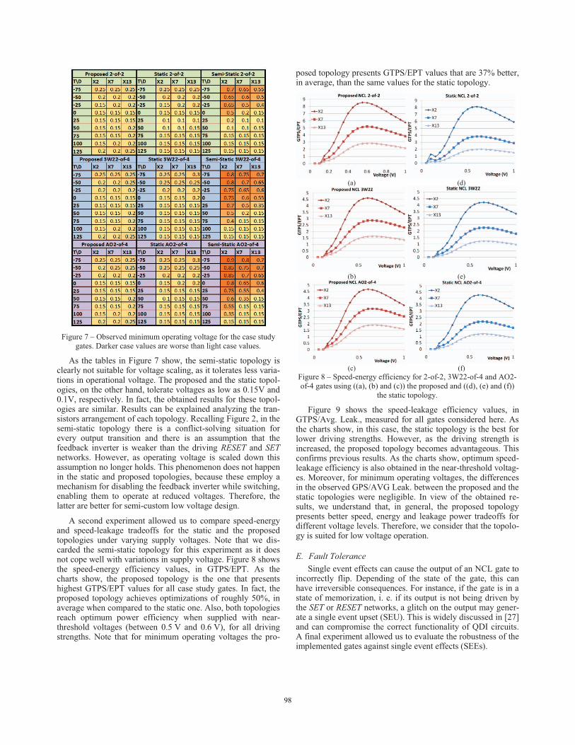
Figure 7 – Observed minimum operating voltage for the case study
gates. Darker case values are worse than light case values.
As the tables in Figure 7 show, the semi-static topology is clearly not suitable for voltage scaling, as it tolerates less varia-tions in operational voltage. The proposed and the static topol-ogies, on the other hand, tolerate voltages as low as 0.15V and 0.1V, respectively. In fact, the obtained results for these topol-ogies are similar. Results can be explained analyzing the tran-sistors arrangement of each topology. Recalling Figure 2, in the semi-static topology there is a conflict-solving situation for every output transition and there is an assumption that the feedback inverter is weaker than the driving RESET and SET networks. However, as operating voltage is scaled down this assumption no longer holds. This phenomenon does not happen in the static and proposed topologies, because these employ a mechanism for disabling the feedback inverter while switching, enabling them to operate at reduced voltages. Therefore, the latter are better for semi-custom low voltage design.
A second experiment allowed us to compare speed-energy and speed-leakage tradeoffs for the static and the proposed topologies under varying supply voltages. Note that we dis-carded the semi-static topology for this experiment as it does not cope well with variations in supply voltage. Figure 8 shows the speed-energy efficiency values, in GTPS/EPT. As the charts show, the proposed topology is the one that presents highest GTPS/EPT values for all case study gates. In fact, the proposed topology achieves optimizations of roughly 50%, in average when compared to the static one. Also, both topologies reach optimum power efficiency when supplied with near-threshold voltages (between 0.5 V and 0.6 V), for all driving strengths. Note that for minimum operating voltages the pro-
posed topology presents GTPS/EPT values that are 37% better, in average, than the same values for the static topology.
(a) (d)
( )
(b) (e) ( )
(c) (f)
Figure 8 – Speed-energy efficiency for 2-of-2, 3W22-of-4 and AO2-of-4 gates using ((a), (b) and (c)) the proposed and ((d), (e) and (f))
the static topology.
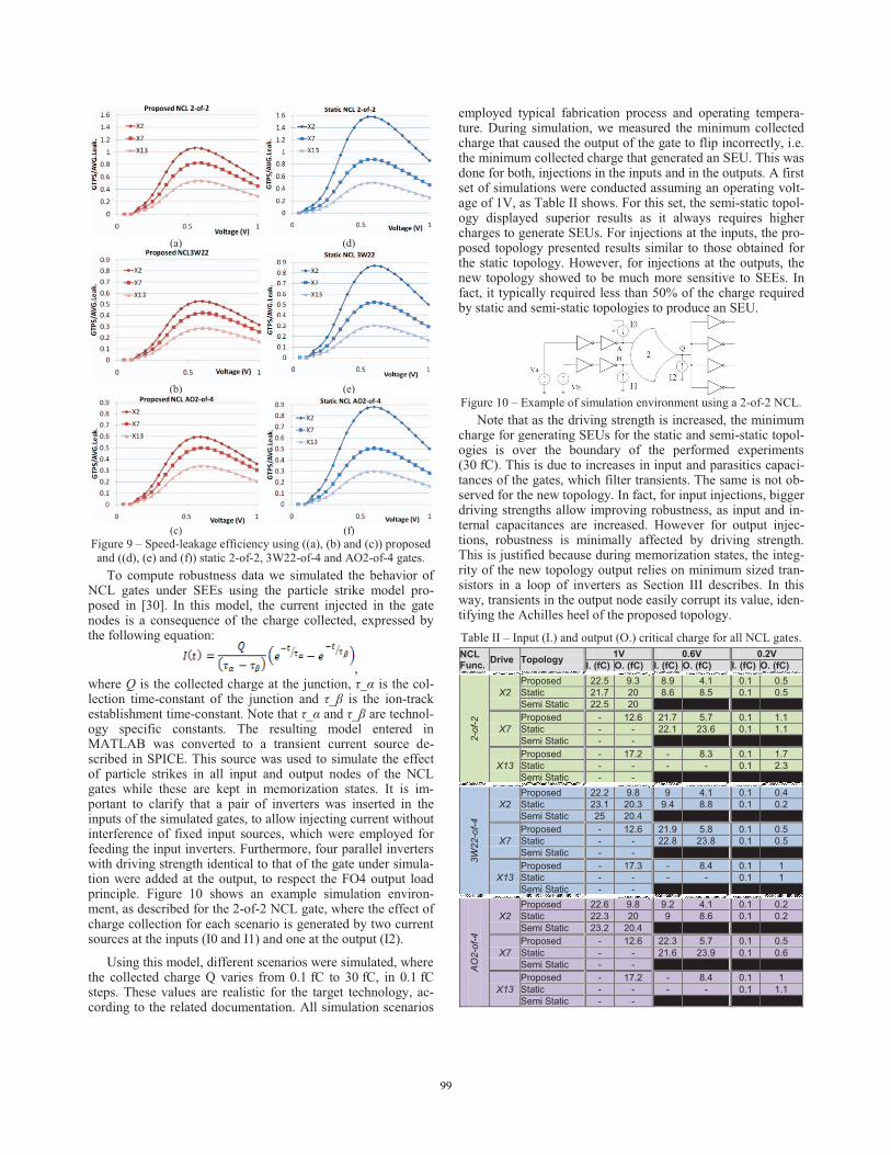
Figure 9 shows the speed-leakage efficiency values, in GTPS/Avg. Leak., measured for all gates considered here. As the charts show, in this case, the static topology is the best for lower driving strengths. However, as the driving strength is increased, the proposed topology becomes advantageous. This confirms previous results. As the charts show, optimum speed-leakage efficiency is also obtained in the near-threshold voltag-es. Moreover, for minimum operating voltages, the differences in the observed GPS/AVG Leak. between the proposed and the static topologies were negligible. In view of the obtained re-sults, we understand that, in general, the proposed topology presents better speed, energy and leakage power tradeoffs for different voltage levels. Therefore, we consider that the topolo-gy is suited for low voltage operation.
E. Fault Tolerance Single event effects can cause the output of an NCL gate to
incorrectly flip. Depending of the state of the gate, this can have irreversible consequences. For instance, if the gate is in a state of memorization, i. e. if its output is not being driven by the SET or RESET networks, a glitch on the output may gener-ate a single event upset (SEU). This is widely discussed in [27] and can compromise the correct functionality of QDI circuits. A final experiment allowed us to evaluate the robustness of the implemented gates against single event effects (SEEs).
98
(a) (d) ( )
(b) (e) ( )
( )
(c) (f)
Figure 9 – Speed-leakage efficiency using ((a), (b) and (c)) proposed and ((d), (e) and (f)) static 2-of-2, 3W22-of-4 and AO2-of-4 gates.
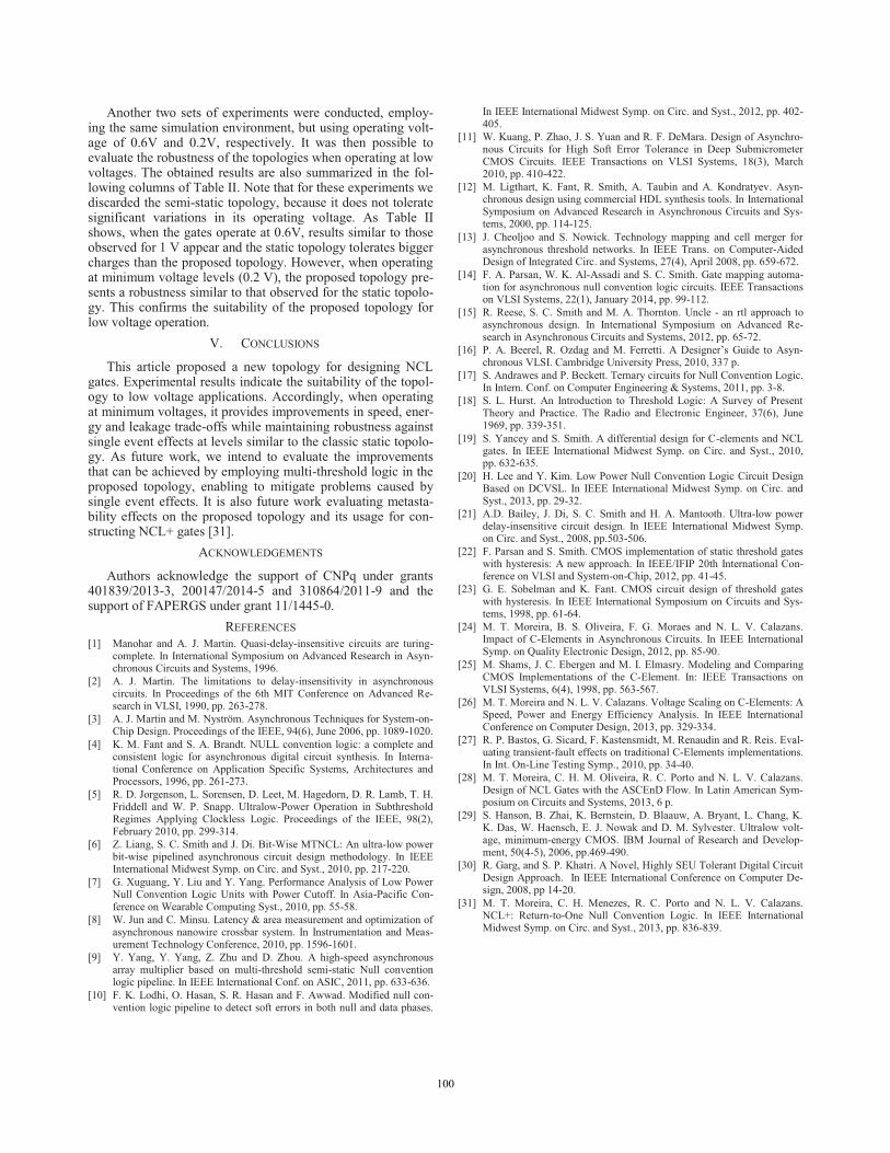
To compute robustness data we simulated the behavior of NCL gates under SEEs using the particle strike model pro-posed in [30]. In this model, the current injected in the gate nodes is a consequence of the charge collected, expressed by the following equation:
, where Q is the collected charge at the junction, τ_α is the col-lection time-constant of the junction and τ_β is the ion-track establishment time-constant. Note that τ_α and τ_β are technol-ogy specific constants. The resulting model entered in MATLAB was converted to a transient current source de-scribed in SPICE. This source was used to simulate the effect of particle strikes in all input and output nodes of the NCL gates while these are kept in memorization states. It is im-portant to clarify that a pair of inverters was inserted in the inputs of the simulated gates, to allow injecting current without interference of fixed input sources, which were employed for feeding the input inverters. Furthermore, four parallel inverters with driving strength identical to that of the gate under simula-tion were added at the output, to respect the FO4 output load principle. Figure 10 shows an example simulation environ-ment, as described for the 2-of-2 NCL gate, where the effect of charge collection for each scenario is generated by two current sources at the inputs (I0 and I1) and one at the output (I2).
Using this model, different scenarios were simulated, where the collected charge Q varies from 0.1 fC to 30 fC, in 0.1 fC steps. These values are realistic for the target technology, ac-cording to the related documentation. All simulation scenarios
employed typical fabrication process and operating tempera-ture. During simulation, we measured the minimum collected charge that caused the output of the gate to flip incorrectly, i.e. the minimum collected charge that generated an SEU. This was done for both, injections in the inputs and in the outputs. A first set of simulations were conducted assuming an operating volt-age of 1V, as Table II shows. For this set, the semi-static topol-ogy displayed superior results as it always requires higher charges to generate SEUs. For injections at the inputs, the pro-posed topology presented results similar to those obtained for the static topology. However, for injections at the outputs, the new topology showed to be much more sensitive to SEEs. In fact, it typically required less than 50% of the charge required by static and semi-static topologies to produce an SEU.
Figure 10 – Example of simulation environment using a 2-of-2 NCL.
Note that as the driving strength is increased, the minimum charge for generating SEUs for the static and semi-static topol-ogies is over the boundary of the performed experiments (30 fC). This is due to increases in input and parasitics capaci-tances of the gates, which filter transients. The same is not ob-served for the new topology. In fact, for input injections, bigger driving strengths allow improving robustness, as input and in-ternal capacitances are increased. However for output injec-tions, robustness is minimally affected by driving strength. This is justified because during memorization states, the integ-rity of the new topology output relies on minimum sized tran-sistors in a loop of inverters as Section III describes. In this way, transients in the output node easily corrupt its value, iden-tifying the Achilles heel of the proposed topology. Table II – Input (I.) and output (O.) critical charge for all NCL gates. NCL Func. Drive Topology 1V 0.6V 0.2V
I. (fC) O. (fC) I. (fC) O. (fC) I. (fC) O. (fC)
2-of
-2
X2 Proposed 22.5 9.3 8.9 4.1 0.1 0.5 Static 21.7 20 8.6 8.5 0.1 0.5 Semi Static 22.5 20
X7 Proposed - 12.6 21.7 5.7 0.1 1.1 Static - - 22.1 23.6 0.1 1.1 Semi Static - -
X13 Proposed - 17.2 - 8.3 0.1 1.7 Static - - - - 0.1 2.3 Semi Static - -
3W22
-of-4
X2 Proposed 22.2 9.8 9 4.1 0.1 0.4 Static 23.1 20.3 9.4 8.8 0.1 0.2 Semi Static 25 20.4
X7 Proposed - 12.6 21.9 5.8 0.1 0.5 Static - - 22.8 23.8 0.1 0.5 Semi Static - -
X13 Proposed - 17.3 - 8.4 0.1 1 Static - - - - 0.1 1 Semi Static - -
AO
2-of
-4
X2 Proposed 22.6 9.8 9.2 4.1 0.1 0.2 Static 22.3 20 9 8.6 0.1 0.2 Semi Static 23.2 20.4
X7 Proposed - 12.6 22.3 5.7 0.1 0.5 Static - - 21.6 23.9 0.1 0.6 Semi Static - -
X13 Proposed - 17.2 - 8.4 0.1 1 Static - - - - 0.1 1.1 Semi Static - -
99
Another two sets of experiments were conducted, employ-ing the same simulation environment, but using operating volt-age of 0.6V and 0.2V, respectively. It was then possible to evaluate the robustness of the topologies when operating at low voltages. The obtained results are also summarized in the fol-lowing columns of Table II. Note that for these experiments we discarded the semi-static topology, because it does not tolerate significant variations in its operating voltage. As Table II shows, when the gates operate at 0.6V, results similar to those observed for 1 V appear and the static topology tolerates bigger charges than the proposed topology. However, when operating at minimum voltage levels (0.2 V), the proposed topology pre-sents a robustness similar to that observed for the static topolo-gy. This confirms the suitability of the proposed topology for low voltage operation.
V. CONCLUSIONS
This article proposed a new topology for designing NCL gates. Experimental results indicate the suitability of the topol-ogy to low voltage applications. Accordingly, when operating at minimum voltages, it provides improvements in speed, ener-gy and leakage trade-offs while maintaining robustness against single event effects at levels similar to the classic static topolo-gy. As future work, we intend to evaluate the improvements that can be achieved by employing multi-threshold logic in the proposed topology, enabling to mitigate problems caused by single event effects. It is also future work evaluating metasta-bility effects on the proposed topology and its usage for con-structing NCL+ gates [31].
ACKNOWLEDGEMENTS
Authors acknowledge the support of CNPq under grants 401839/2013-3, 200147/2014-5 and 310864/2011-9 and the support of FAPERGS under grant 11/1445-0.
REFERENCES [1] Manohar and A. J. Martin. Quasi-delay-insensitive circuits are turing-
complete. In International Symposium on Advanced Research in Asyn-chronous Circuits and Systems, 1996.
[2] A. J. Martin. The limitations to delay-insensitivity in asynchronous circuits. In Proceedings of the 6th MIT Conference on Advanced Re-search in VLSI, 1990, pp. 263-278.
[3] A. J. Martin and M. Nyström. Asynchronous Techniques for System-on-Chip Design. Proceedings of the IEEE, 94(6), June 2006, pp. 1089-1020.
[4] K. M. Fant and S. A. Brandt. NULL convention logic: a complete and consistent logic for asynchronous digital circuit synthesis. In Interna-tional Conference on Application Specific Systems, Architectures and Processors, 1996, pp. 261-273.
[5] R. D. Jorgenson, L. Sorensen, D. Leet, M. Hagedorn, D. R. Lamb, T. H. Friddell and W. P. Snapp. Ultralow-Power Operation in Subthreshold Regimes Applying Clockless Logic. Proceedings of the IEEE, 98(2), February 2010, pp. 299-314.
[6] Z. Liang, S. C. Smith and J. Di. Bit-Wise MTNCL: An ultra-low power bit-wise pipelined asynchronous circuit design methodology. In IEEE International Midwest Symp. on Circ. and Syst., 2010, pp. 217-220.
[7] G. Xuguang, Y. Liu and Y. Yang. Performance Analysis of Low Power Null Convention Logic Units with Power Cutoff. In Asia-Pacific Con-ference on Wearable Computing Syst., 2010, pp. 55-58.
[8] W. Jun and C. Minsu. Latency & area measurement and optimization of asynchronous nanowire crossbar system. In Instrumentation and Meas-urement Technology Conference, 2010, pp. 1596-1601.
[9] Y. Yang, Y. Yang, Z. Zhu and D. Zhou. A high-speed asynchronous array multiplier based on multi-threshold semi-static Null convention logic pipeline. In IEEE International Conf. on ASIC, 2011, pp. 633-636.
[10] F. K. Lodhi, O. Hasan, S. R. Hasan and F. Awwad. Modified null con-vention logic pipeline to detect soft errors in both null and data phases.
In IEEE International Midwest Symp. on Circ. and Syst., 2012, pp. 402-405.
[11] W. Kuang, P. Zhao, J. S. Yuan and R. F. DeMara. Design of Asynchro-nous Circuits for High Soft Error Tolerance in Deep Submicrometer CMOS Circuits. IEEE Transactions on VLSI Systems, 18(3), March 2010, pp. 410-422.
[12] M. Ligthart, K. Fant, R. Smith, A. Taubin and A. Kondratyev. Asyn-chronous design using commercial HDL synthesis tools. In International Symposium on Advanced Research in Asynchronous Circuits and Sys-tems, 2000, pp. 114-125.
[13] J. Cheoljoo and S. Nowick. Technology mapping and cell merger for asynchronous threshold networks. In IEEE Trans. on Computer-Aided Design of Integrated Circ. and Systems, 27(4), April 2008, pp. 659-672.
[14] F. A. Parsan, W. K. Al-Assadi and S. C. Smith. Gate mapping automa-tion for asynchronous null convention logic circuits. IEEE Transactions on VLSI Systems, 22(1), January 2014, pp. 99-112.
[15] R. Reese, S. C. Smith and M. A. Thornton. Uncle - an rtl approach to asynchronous design. In International Symposium on Advanced Re-search in Asynchronous Circuits and Systems, 2012, pp. 65-72.
[16] P. A. Beerel, R. Ozdag and M. Ferretti. A Designer’s Guide to Asyn-chronous VLSI. Cambridge University Press, 2010, 337 p.
[17] S. Andrawes and P. Beckett. Ternary circuits for Null Convention Logic. In Intern. Conf. on Computer Engineering & Systems, 2011, pp. 3-8.
[18] S. L. Hurst. An Introduction to Threshold Logic: A Survey of Present Theory and Practice. The Radio and Electronic Engineer, 37(6), June 1969, pp. 339-351.
[19] S. Yancey and S. Smith. A differential design for C-elements and NCL gates. In IEEE International Midwest Symp. on Circ. and Syst., 2010, pp. 632-635.
[20] H. Lee and Y. Kim. Low Power Null Convention Logic Circuit Design Based on DCVSL. In IEEE International Midwest Symp. on Circ. and Syst., 2013, pp. 29-32.
[21] A.D. Bailey, J. Di, S. C. Smith and H. A. Mantooth. Ultra-low power delay-insensitive circuit design. In IEEE International Midwest Symp. on Circ. and Syst., 2008, pp.503-506.
[22] F. Parsan and S. Smith. CMOS implementation of static threshold gates with hysteresis: A new approach. In IEEE/IFIP 20th International Con-ference on VLSI and System-on-Chip, 2012, pp. 41-45.
[23] G. E. Sobelman and K. Fant. CMOS circuit design of threshold gates with hysteresis. In IEEE International Symposium on Circuits and Sys-tems, 1998, pp. 61-64.
[24] M. T. Moreira, B. S. Oliveira, F. G. Moraes and N. L. V. Calazans. Impact of C-Elements in Asynchronous Circuits. In IEEE International Symp. on Quality Electronic Design, 2012, pp. 85-90.
[25] M. Shams, J. C. Ebergen and M. I. Elmasry. Modeling and Comparing CMOS Implementations of the C-Element. In: IEEE Transactions on VLSI Systems, 6(4), 1998, pp. 563-567.
[26] M. T. Moreira and N. L. V. Calazans. Voltage Scaling on C-Elements: A Speed, Power and Energy Efficiency Analysis. In IEEE International Conference on Computer Design, 2013, pp. 329-334.
[27] R. P. Bastos, G. Sicard, F. Kastensmidt, M. Renaudin and R. Reis. Eval-uating transient-fault effects on traditional C-Elements implementations. In Int. On-Line Testing Symp., 2010, pp. 34-40.
[28] M. T. Moreira, C. H. M. Oliveira, R. C. Porto and N. L. V. Calazans. Design of NCL Gates with the ASCEnD Flow. In Latin American Sym-posium on Circuits and Systems, 2013, 6 p.
[29] S. Hanson, B. Zhai, K. Bernstein, D. Blaauw, A. Bryant, L. Chang, K. K. Das, W. Haensch, E. J. Nowak and D. M. Sylvester. Ultralow volt-age, minimum-energy CMOS. IBM Journal of Research and Develop-ment, 50(4-5), 2006, pp.469-490.
[30] R. Garg, and S. P. Khatri. A Novel, Highly SEU Tolerant Digital Circuit Design Approach. In IEEE International Conference on Computer De-sign, 2008, pp 14-20.
[31] M. T. Moreira, C. H. Menezes, R. C. Porto and N. L. V. Calazans. NCL+: Return-to-One Null Convention Logic. In IEEE International Midwest Symp. on Circ. and Syst., 2013, pp. 836-839.
100


![Analysis and Design of a Low Noise Shunt-Shunt CMOS ... · The shunt-shunt TIA topology is shown in Fig. 1 [6]. This topology is composed by a voltage amplifier with a transfer function](https://static.fdocuments.net/doc/165x107/5ea54e44e44a2608a21306f1/analysis-and-design-of-a-low-noise-shunt-shunt-cmos-the-shunt-shunt-tia-topology.jpg)