A nanoporous silicon nitride membrane using a two-step ... · A nanoporous silicon nitride membrane...
9
A nanoporous silicon nitride membrane using a two-step lift-off pattern transfer with thermal nanoimprint lithography This article has been downloaded from IOPscience. Please scroll down to see the full text article. 2012 J. Micromech. Microeng. 22 045012 (http://iopscience.iop.org/0960-1317/22/4/045012) Download details: IP Address: 192.38.67.112 The article was downloaded on 07/08/2012 at 06:18 Please note that terms and conditions apply. View the table of contents for this issue, or go to the journal homepage for more Home Search Collections Journals About Contact us My IOPscience
Transcript of A nanoporous silicon nitride membrane using a two-step ... · A nanoporous silicon nitride membrane...

A nanoporous silicon nitride membrane using a two-step lift-off pattern transfer with thermal
nanoimprint lithography
This article has been downloaded from IOPscience. Please scroll down to see the full text article.
2012 J. Micromech. Microeng. 22 045012
(http://iopscience.iop.org/0960-1317/22/4/045012)
Download details:
IP Address: 192.38.67.112
The article was downloaded on 07/08/2012 at 06:18
Please note that terms and conditions apply.
View the table of contents for this issue, or go to the journal homepage for more
Home Search Collections Journals About Contact us My IOPscience

IOP PUBLISHING JOURNAL OF MICROMECHANICS AND MICROENGINEERING
J. Micromech. Microeng. 22 (2012) 045012 (8pp) doi:10.1088/0960-1317/22/4/045012
A nanoporous silicon nitride membraneusing a two-step lift-off pattern transferwith thermal nanoimprint lithographyBhargav P Nabar1, Zeynep Celik-Butler1, Brian H Dennis2
and Richard E Billo3
1 Department of Electrical Engineering and Nanotechnology Research and Teaching Facility,University of Texas at Arlington, Arlington, TX 76019, USA2 Department of Mechanical and Aerospace Engineering, University of Texas at Arlington, Arlington,TX 76019, USA3 Department of Industrial and Manufacturing Engineering, University of Texas at Arlington, Arlington,TX 76019, USA
E-mail: [email protected]
Received 7 July 2011, in final form 20 November 2011Published 15 March 2012Online at stacks.iop.org/JMM/22/045012
AbstractNanoimprint lithography is emerging as a viable contender for fabrication of large-scale arraysof 5–500 nm features. A fabrication process for the realization of thin nanoporous membranesusing thermal nanoimprint lithography is presented. Suspended silicon nitride membraneswere fabricated by low-pressure chemical vapor deposition (LPCVD) in conjunction with apotassium hydroxide-based bulk micromachining process. Nanoscale features were imprintedinto a commercially available thermoplastic polymer resist using a prefabricated silicon mold.The pattern was reversed and transferred to a thin aluminum oxide layer by means of a noveltwo-stage lift-off technique. The patterned aluminum oxide was used as an etch mask in aCHF3/He-based reactive ion etch process to transfer the pattern to silicon nitride. Highlydirectional etch profiles with near vertical sidewalls and excellent Si3N4/Al2O3 etch selectivitywere observed. One micrometer thick porous membranes with varying dimensions of250 × 250 μm2 to 450 × 450 μm2 and a pore diameter of 400 nm have been engineered andevaluated. Results indicate that the membranes have consistent nanopore dimensions andprecisely defined porosity, which makes them ideal as gas exchange interfaces in bloodoxygenation systems as well as other applications such as dialysis.
(Some figures may appear in colour only in the online journal)
1. Introduction
Nanoporous membranes fabricated from organic and inorganicmaterials have garnered widespread interest in the scientificcommunity. Such membranes are primarily used for selectivemass transfer [1–3]. Owing to their unique physical propertiesat nanometer scale dimensions, nanoporous membranes alsofind applications such as biosensing and chemical sensing[4–7].
Typical requirements for porous membranes are precisepore placement, uniform pore density over a wide area andmechanical robustness to withstand frequently encountered
differential pressures and cyclic loadings. Pore blockageduring either fabrication or operation and subsequentimpedance to matter transfer is another common problemfor porous membranes that must be addressed. Additionalapplication-specific requirements such as pore depth, porediameter, membrane surface energy and surface texture placestringent demands on the fabrication process. A number oftechniques have been developed to meet these constraints witheach offering unique advantages and drawbacks.
Fabrication of porous membranes using electron beamlithography [8] and focused ion beam [9] has been reported.Porous membranes with a pore diameter of 50 nm and
0960-1317/12/045012+08$33.00 1 © 2012 IOP Publishing Ltd Printed in the UK & the USA

J. Micromech. Microeng. 22 (2012) 045012 B P Nabar et al
(a) (b)
Figure 1. Silicon mold used for the nanoimprint lithography process. (a) SEM image. (b) AFM image. (Image courtesy of NILT, Denmark.)
1.8 μm have been achieved. These techniques offer significantadvantages in terms of pore placement precision and thefabricated pores offer unimpeded mass transfer. Nevertheless,large-area production is not possible and as such, thesetechniques are impractical in terms of cost and time for massfabrication of high-pore density membranes.
Heavy ion track etching is an established technique used tofabricate nanoporous membranes from organic polymers suchas PCTE [10]. However, the inherent random nature of theheavy ions in the plasma environment precludes the formationof well-defined arrays of nanopores. Nanoporous membranesfabricated using interference lithography [11] have advantagessuch as uniform pore size and distribution, in addition toregular array arrangement of nanopores. The complexity ofthe process is the only limiting factor preventing widespreadusage of the technique for porous membrane production.
Nanoimprint lithography (NIL), developed by Chou et al[12], provides an excellent solution to each of the shortcomingsof the processes discussed above. NIL draws on the strengthsof each of these processes and offers the advantage ofbeing able to simultaneously fabricate a large number ofnanoscale features with precise dimensions, high aspectratio and accurate placement. Combined with conventionalCMOS pattern transfer techniques, mass fabrication of wide-area arrays of nanometer features with high-aspect ratios isachievable at a fraction of the cost as compared to the otherprocesses [13]. This makes NIL the method of choice forfabrication of nanoporous membranes in this present work.
The imprint resist used for NIL is typically a thermoplasticpolymer such as PMMA. Such resists have been found to havelimited etch resistance for dry etch processes [14]. These resistsare better suited for lift-off-based techniques, which have beensuccessfully demonstrated [5]. Another concern with NIL isthe initial cost and complexity involved in the fabrication ofthe mold or the stamp. In order to adapt a fabricated siliconNIL mold designed for a direct etch process to a lift-off-basedprocess, a two-stage lift-off process was developed. A similartechnique has been previously demonstrated by Song et al [15]to obtain 146 nm diameter hole patterns of unspecified depthon a Si substrate. They have used UV-based nanoimprinting intheir work. Here, we have utilized an alternate nanoimprinting
method, namely thermal, and optimized the process to obtainthrough holes across a 1 μm thick Si3N4 membrane. Thisrequired precise pattern transfer accuracy across two lift-offprocesses and sufficient etch selectivity between the membraneand the etch mask to achieve holes with high-aspect ratios.
In this work, we present a fabrication technique for abulk micromachined, nanoporous silicon nitride membranecontaining a wide-area, highly periodic array of high-aspectratio, through-membrane and straight-walled nanopores. Wehave used NIL in conjunction with a pattern reversallithography technique, which is also described herein. Usingthe described process, we have been able to successfullyfabricate 1 μm thick nanoporous silicon nitride membraneshaving a pore diameter of 400 nm with a pitch of 500 nm.
2. Experimental methods
2.1. Silicon mold
A three inch (1 0 0) silicon wafer patterned with pillar-shapedstructures of 200 nm in diameter, 500 nm pitch and 120 nmin height was acquired from NILT technologies, Denmark(www.nilt.com). The dimensions of the mold features werechosen such that the resulting nanoporous membranes wouldhave pore dimensions optimized for selective gas exchangebetween a liquid–gaseous interface. The mold was coatedwith a NXT 100 antiadhesion layer from Nanonex Inc. tofacilitate separation of the mold from the nanoimprint resistafter imprinting without damage (figure 1).
2.2. Silicon nitride growth and backside patterning
The process started with the deposition of a thin silicon nitride(Si3N4) layer. The Si3N4 was deposited using low-pressurechemical vapor deposition (LPCVD) on both sides of a3′′(1 0 0) silicon wafer at a temperature of 835 ◦C and a pressureof 250 mTorr. Dichlorosilane (100 sccm) and ammonia(20 sccm) were used as the process gases, resulting in growthof a 1 ± 0.05 μm thick low-stress Si3N4 at a rate of200 nm h−1. Next, NR9 3000P photoresist from FuturrexInc. was spin coated on the backside to achieve a thickness
2

J. Micromech. Microeng. 22 (2012) 045012 B P Nabar et al
(a)
(b)
Figure 2. (a) Solid model showing the membrane array: green—Si3N4, brown—silicon. (b) Solid model cross section.
of 3 μm, followed by a prebake and UV exposure todefine the membrane windows. After a postexposure, theresist was developed using the RD6 developer. As shownin figure 2, the pattern transferred from the photomask tothe photoresist consisted of arrays of square-shaped featureshaving dimensions of 250 × 250 μm2, 350 × 350 μm2 and450 × 450 μm2. These patterns were transferred fromthe photoresist to the underlying silicon nitride by meansof a fluorine-based reactive ion etch (RIE) process, usingtetrafluoromethane (CF4) at 130 mTorr pressure, and 100 WRIE power. An etch rate of 30 nm min−1 was obtained.
2.3. Nanoimprint lithography and pattern reversal process
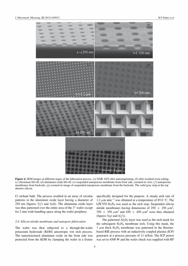
Nanoimprinting step started with spin coating a 180 nm thickNXR 1025 thermal imprint resist from Nanonex Inc. on thefront-side silicon nitride. The wafer was then baked at 150 ◦Cfor 3 min on a hotplate to drive out all the solvent. The siliconnanoimprint mold was placed in contact with the nanoimprintresist and both wafers were loaded into a Nanonex NXB200 nanoimprinter. The wafers were heated to a temperatureof 130 ◦C and were compressed at an initial pressure of120 psi. After holding the pressure constant for a few seconds,it was increased to 200 psi and thermal resist was imprinted for30 s. Thereafter, the temperature was slowly reduced to roomtemperature, allowing the resist to solidify. The wafers weresubsequently separated without much difficulty owing to theantiadhesion layer coated on the silicon mold. The resultantfeatures are schematically illustrated in figure 3(a). The SEMphoto is shown in figure 4(a).
The imprinting process resulted in an intentional residualresist with a thickness of 60–70 nm due to the difference inthe thermal imprint resist thickness and the features on themold. This residual resist was etched in a reactive ion etcher inAr/O2 plasma, at a pressure of 11 mTorr and with RF powerof 40 W at 13.56 MHz to realize an anisotropic etch profile.Figures 3(b) and 4(b) depict the structures at the end of thisstage.
Next, an 85 nm chromium layer was deposited on thethermal imprint resist in an electron beam evaporator, at achamber pressure of 2.0 × 10⁻⁸ mTorr (figure 3(c)). Thedeposition rate was maintained at a constant 0.15 nm s−1 rateby means of controlling the electron beam current. This servesas an intermediary layer to transfer the pattern from the thermalresist to the aluminum oxide (Al2O3) mask layer. The Cr film
(a) (e)
(b) ( f )
(c) (g)
(d ) (h)
Figure 3. Schematic illustration of the nanoporous membranefabrication process. (a) NXR1020 spin coating and nanoimprinting,(b) residual resist ashing, (c) chromium evaporation, (d) chromiumlift-off, (e) aluminum oxide deposition, ( f ) aluminum oxide lift-off,(g) backside KOH etch, (h) reactive ion etch to realize nanopores.
was then patterned by means of a lift-off process in acetonebath, resulting in Cr pillars of 210 nm in diameter and 85 nm inheight as shown in figures 3(d) and 4(c). After that, a thin filmof Al2O3 was sputtered on top of the chromium pillars in anultra-high vacuum RF magnetron sputter deposition system.The process pressure was set to 5.0 mTorr and the depositionwas carried out at a RF power of 150.0 W. A total of 55 nmof Al2O3 was deposited at a deposition rate of 1.04 nm min−1
(figure 3(e)). Next, the Al2O3 was patterned by means of asecond lift-off process, by placing the wafer in a CR 1020
3
J. Micromech. Microeng. 22 (2012) 045012 B P Nabar et al
(a) (b)
(c) (d)
(e) ( f )
(g)
Figure 4. SEM images at different stages of the fabrication process. (a) NXR 1025 after nanoimprinting, (b) after residual resist ashing,(c) chromium lift-off, (d) aluminum oxide lift-off, (e) suspended nanoporous membrane from front side, zoomed-in view, ( f ) nanoporousmembranes from backside, (g) zoomed-in image of suspended nanoporous membrane from the backside. The solid gray strip at the topdenotes silicon.
Cr etchant bath. The process resulted in an array of circularpatterns in the aluminum oxide layer having a diameter of250 nm (figures 3( f ) and 4(d)). The aluminum oxide layerwas thus patterned over the entire area of the 3′′ wafer exceptfor 2 mm wide handling space along the wafer periphery.
2.4. Silicon nitride membrane and nanopore fabrication
The wafer was then subjected to a through-the-waferpotassium hydroxide (KOH) anisotropic wet etch process.The nanostructured aluminum oxide on the front side wasprotected from the KOH by clamping the wafer in a fixture
specifically designed for the purpose. A steady etch rate of1.2 μm min−1 was obtained at a temperature of 85.0 ◦C. TheLPCVD Si3N4 was used as the etch stop. Suspended siliconnitride membranes having dimensions of 250 × 250 μm2,350 × 350 μm2 and 450 × 450 μm2 were thus obtained(figures 3(g) and 4( f )).
The patterned Al2O3 layer was used as the etch mask forthe subsequent Si3N4 membrane etch. Using this mask, the1 μm thick Si3N4 membrane was patterned in the fluorine-based RIE process with an inductively coupled plasma (ICP)generator at a process pressure of 11 mTorr. The ICP powerwas set to 4500 W and the wafer chuck was supplied with RF
4

J. Micromech. Microeng. 22 (2012) 045012 B P Nabar et al
power of 35 W. The process gases used were trifluoromethane(CHF3) and helium (He). The etch process yielded a verticaletch rate of 63.8 nm min−1 for the LPCVD silicon nitride withsufficient anisotropy. Four hundred nanometer wide, 1 μmdeep pores were obtained as a result of this etch process, asdepicted in figure 3(h).
The complete fabrication process is schematicallyillustrated in figure 3. The SEM photos of nanoporousmembrane reveal excellent periodicity and uniformity. Fromthe SEM photos of the nanopores on the front-side (figure 3(e))and the back-side (figure 3(g)), it is clear that the pores are allthe way through the membrane.
3. Results and discussion
The two-stage lift-off pattern reversal technique described herewas developed for two chief reasons. First, the nanoimprintresist did not possess sufficient selectivity over Al2O3 in afluorine-based RIE process. Attempts to etch Al2O3 in a wetetch process with dilute hydrofluoric acid resulted in severeundercutting of the nanoimprint resist causing it to delaminatefrom the Al2O3 layer during the etch process. Therefore, itwas concluded that a direct etch process would not be afeasible option for patterning of the Al2O3 layer. Indirectpatterning using a conventional lift-off process would meanthat the polarity of the silicon mold would have to be reversed,effectively necessitating fabrication of a new mold with holesinstead of pillars. Such a mold, however, is harder to use dueto difficulties in cleaning it, and would most likely to have ashorter life-time than a pillar mold because it would be morechallenging to separate it from the resist after the nanoimprintprocess
Pattern reversal techniques for photolithography havebeen well established. These techniques were developed toprovide an extra degree of flexibility to the process designengineer. By varying the photoresist processing parameters,the same photomask can be used for direct and reverse patterntransfer. The NIL pattern reversal technique accomplishesthe same outcome by reversing the polarity of the patternon the nanoimprint mold with the help of an intermediateetch mask deposited on the substrate. The pattern reversalis accomplished by means of two consecutive lift-off patterntransfer processes. This is illustrated in figure 3. The patternednanoimprint resist is coated with a thin film of template layer1(TL1). The first lift-off process is a conventional lift-offprocess that results in a mirror image of the mold patternon the template layer 1. Next, the patterned template layer 1 iscoated with a thin film of template layer 2 (TL2). The sampleis then placed in an etchant to remove TL1. This results inpatterning of TL2 by means of a lift-off. If this method wereto be analogized to a conventional lift-off process, TL1 wouldbe the ‘lift-off resist’ and the etchant would be the ‘resistremover’.
The selection of TL2 is primarily governed by therequirements imposed by its function in the device orthe fabrication process. In the present case, high etchselectivity over silicon nitride in a fluorine-based RIE processnecessitated the selection of aluminum oxide as TL2. The
Figure 5. Percentage error in the nanopore dimension as a functionof aluminum oxide to chromium thickness ratio.
two-stage lift-off process, however, imposes another importantrequirement on the selection of TL2, mainly that it should havesufficiently high-etch resistance to the chemical etchant usedto remove TL1. A nontrivial etch rate for TL2 in the etchantcan cause pattern distortion, as the removal process for TL1is isotropic. Thus, TL1 has to be chosen such that it readilydissolves in a wet etchant that has a very low etch rate for TL2.In the present case, Al2O3 exhibited a negligible etch rate inCR 1020, the etchant used for removing chromium (etch rate0.2 nm s−1).
The thickness of TL1 could also be influenced by its rolein the device/process. In addition, the ratio of thicknessesof TL2 to TL1 has been found to influence pattern transferaccuracy. As is observed in conventional lift-off processes, ahigh TL2 to TL1 thickness ratio leads to a larger error in thepattern dimension (figure 5).
This error could possibly stem from a conformaldeposition of sputtered aluminum oxide on chromium. Fora successful lift-off, any deposition of aluminum oxide on thesidewalls of the chromium pillar would first need to be removedfor the etchant to access and dissolve chromium. Therefore,the time required for lift-off would be greater, considering thatAl2O3 has a very slow etch rate in CR1020. It was observedthat for Al2O3 to Cr thickness ratios greater than 0.4, the timerequired to dissolve Cr coated with Al2O3 was considerablymore compared to that necessary to dissolve bare Cr of thesame thickness. Moreover, ultrasonic agitation was necessaryto achieve lift-off uniformity over the entire wafer. The greatertime spent by the wafer in the etchant could cause patterndistortion of Al2O3. In general, the ideal method for depositionof TL2 would be one that is nonconformal, such as thermalor electron beam evaporation. In addition, if a lower thicknessratio of TL2 to TL1 can be tolerated, the resulting thinnersidewall would be easier to remove thus minimizing the error.
The sidewall profile of the Cr pillars was observed ina SEM by tilting the sample to 70◦. The chromium pillarsdisplay a ‘mushroom’ like structure as seen in figure 6(a). Thetop half of the pillar is noticeably broader than the bottom.
5

J. Micromech. Microeng. 22 (2012) 045012 B P Nabar et al
(a) (b)
Figure 6. (a) Chromium lift-off stage showing ‘mushroom’ shaped pillars. Inset: magnified image. (b) Nanoimprint resist after residualresist ashing showing the positive sidewall profile.
Figure 7. Reactive ion etch profile of nanopores in a 1 μm thick silicon nitride layer on silicon.
This is similar to a negative slope profile or an undercutprofile typically observed in the sidewalls of conventionallift-off resists that are optimized for liftoff-based patterning.The mushroom structure causes a shadow effect during thedeposition of Al2O3, thus minimizing the formation of anAl2O3 layer on the Cr pillar sidewall. The etchant can thenaccess and remove the Cr in minimal time resulting in moreaccurate pattern transfer.
The negative sidewall slope in the chromium pillar ispossibly an artifact of the Ar/O2 etching process used forremoving the residual resist after nanoimprinting. As seenin figure 6(b), the nanopore in the imprinted resist hasa positive sidewall slope after residual resist etching. Thepositive sidewall slope in the imprint resist translates to anegative sidewall slope in the chromium pillar, resulting in thecharacteristic mushroom shape. It was observed that a ratio of0.3 for the Al2O3/Cr thickness resulted in negligible distortionof the pattern dimensions. In addition, the time required forlift-off was significantly shorter and no ultrasonic agitationwas necessary. The results point to the conclusion that patterndistortion in TL2 in the two-stage lift-off process can be limitedby engineering of the sidewall profile of TL1 to obtain anegative sidewall slope.
Pattern transfer from the aluminum oxide to siliconnitride was achieved using a specially formulated RIEprocess. Trifluoromethane (CHF3) was the primary etchant
gas providing a source of fluorine radicals, while heliumwas added for dilution and to improve anisotropy. It wasassumed that usage of a fluorine-deficient fluorocarbon suchas trifluoromethane as opposed to tetrafluoromethane (CF4)would limit the availability of fluorine radicals per unit volumeof chamber atmosphere thus lowering the lateral etch rateand improving anisotropy [16]. Addition of helium-facilitatedefficient transport of the reactant species and removal ofvolatile etch products. A low-chamber process pressure furtherimproved the directionality, while independent control of theplasma density with the inductively coupled plasma generatorimproved selectivity. As shown in figure 7, near verticalsidewalls for the nanopores were obtained (sidewall angle89.4◦). The vertical to lateral etch rate ratio was 12.76 resultingin cylindrical pores with a pore diameter of 400 nm anda separation of 100 nm. The etch selectivity of Si3N4 toAl2O3 was found to be 24.75:1. To the best of our knowledge,the highest reported selectivity for silicon dioxide over siliconnitride is 30:1 in the plasma etch process [17]. Our resultsdemonstrate the practicality of Al2O3 as an alternative maskfor Si3N4 in a fluorine-based RIE process.
Postfabrication, the nanoporous membranes wereexamined for cracks and point defects. Figure 8(a) showsmembrane placement and sampling locations on a 3′′ diameterwafer.
6

J. Micromech. Microeng. 22 (2012) 045012 B P Nabar et al
(a)
(b)
Figure 8. (a) Wafer layout and sampling location nomenclature. (b) Individual die.
Figure 9. Point defects on a 10 μm × 10 μm sample area of asuspended silicon nitride membrane.
Figure 8(b) shows an individual die on the wafer. Eachdie contains 91 suspended nanoporous membranes for atotal of 364 membranes on the entire wafer. Each of themembranes was examined under a Nomarski microscope. All364 membranes were found to be intact after the completionof the process.
A single membrane from each die—identified accordingto the nomenclature presented in figure 8(a)—was imagedusing a scanning electron microscope for point defects. Anarea of 10 μm × 10 μm was chosen for characterization.Figure 9 shows the different point defects identified.
Observations at different points on the wafer as outlinedby the nomenclature in figures 8(a) and 9 yielded the resultsshown in table 1.
The areal defect density was calculated as
Area of a single pore × average number of defective pores
Sample area.
(1)
Accordingly, the areal defect density for the sampled areaswas found to be 0.064. The observed standard deviationwas significant at 27% and suggests that the detected
Table 1. Defect occurrences in 10 μm × 10 μm sample areas on asingle wafer.
Position of the sample area
Top Bottom Left Right
Total no of pores 400 400 400 400Defect events 13 27 24 22Connected pores (a) 28 70 63 56Malformed pores (b) 2 0 1 1Total no. of damaged pores (a+b) 30 70 64 57% Damaged pores 7.5 17.5 16 14.25Wafer average% damaged pores 13.81% Standard deviation in no of 27.66
damaged pores across wafer
point defects are the result of randomly occurring processvariations not inherent to the process design. Some of theidentified process variations are local nonuniformities in thenanoimprint resist thickness from particulate residue andvariations in the thickness of the nanoimprint resist afterresidual resist etching. Other reasons include artifacts from thenanoimprinting process due to local failure of the antiadhesionlayer after repeated use and variations in the thickness of theCr/Al2O3 resulting in improper lift-off. A significant reductionin the occurrences of point defects is thought to be possible byimproving process environment and equipment repeatabilitysuch as that found in a commercial foundry.
The membranes were further characterized for variationsin pore diameter across the wafer. The diameter was measuredfrom images taken with a scanning electron microscope.The sampling locations were as illustrated in figure 8(a). Asummary of the observations is presented in table 2.
As is evident from the per cent standard deviation,the variation in nanopore diameter is quite insignificant.The observations listed in table 2 also include human andinstrument error in scanning electron microscopy, stemmingfrom image focusing and diameter judgment from the obtainedimage using software-based analysis tools. As such, excellentuniformity in the nanopore diameter is observed across a 3′′
wafer. This observation suggests that within the limits ofreasonable process latitude, variation in nanopore diameteris more tolerant of the process variations listed previously.This demonstrates the efficacy of the two-step lift-off pattern
7

J. Micromech. Microeng. 22 (2012) 045012 B P Nabar et al
Table 2. Variation in nanopore diameter across a 3′′ diameter wafer.
Position
Top Bottom Left Right
Center Edge Center Edge Center Edge Center Edge
Average diameter (nm) 387 382 389 383 384 389 387 384Wafer average (nm) 385.63% S.D 0.71
transfer process toward pattern size uniformity over a largearea.
4. Conclusion
Nanoporous silicon nitride membranes have been fabricatedusing thermal nanoimprint lithography in conjunction with aCr-lift-off technique. Development of a novel two-stage lift-off process to accomplish pattern transfer from nanoimprintresist to silicon nitride is reported. A highly directionalfluorine-based reactive ion-etch process for defining nanoscaledimensions is described. Viability of amorphous aluminumoxide as a suitable etch mask is demonstrated for reactive ionetching of silicon nitride. Nanoporous membranes of 1 μmthickness with highly ordered nanopores of 400 nm diameterhave been achieved. The nanoporous membranes described inthis work were meant to serve as gas exchange interfaces inblood oxygenation systems.
Acknowledgment
This work was in part supported by UTA/UTD/TI/THREMedical Technology Research Program.
References
[1] Desai T, Hansford D, Leoni L, Essenpreis M and Ferrari M2000 Nanoporous anti-fouling silicon membranes forbiosensor applications Biosens. Bioelectron. 15 453–62
[2] Fissel W, Humes H, Fleischman A and Roy S 2007 Dialysisand nanotechnology: now, 10 years, or never ? Blood. Purif.25 12–7
[3] Yang S, Ryu I, Kim H, Kim J, Jang S and Russell T 2006Nanoporous membranes with ultrahigh selectivity and fluxfor the filtration of viruses Adv. Mater. 18 709–12
[4] Heins E, Siwy Z, Baker L and Martin C 2005 Detecting singleporphyrin molecules in a conically shaped syntheticnanopore Nano. Lett. 5 1824–9
[5] Li Q, Luo G, Feng J, Zhou Q, Zhang L and Zhu Y 2001Amperometric detection of glucose with glucose oxidaseabsorbed on porous nanocrystalline TiO2 thin filmElectroanalysis 13 413–6
[6] Singh S, Arya S, Pandey P, Malhotra B, Saha S, Sreenivas Kand Gupta V 2007 Cholesterol biosensor based on RFsputtered zinc oxide nanoporous thin film Appl. Phys. Lett.91 063901
[7] Ilwhan O, Monty C, Shannon M and Masel R 2007Microfabricated electrochemical sensor for chemicalwarfare agents: smaller is better Solid-State Sensors,Actuators and Microsystem Conf. p 971
[8] Deshmukh M, Ralph D C, Thomas M and Silcox J 1999Nanofabrication using a stencil mask Appl. Phys. Lett.75 1631–3
[9] Ambravaneswaran V, Uthamaraj S, Celik-Butler Z,Eberhart R, Chuong C, Billo R and Savitt M 2008Micromachined nanoporous membranes for bloodoxygenation systems 8th IEEE Conf. on Nanotechnology(Arlington, TX, USA) p 201
[10] Ferain E and Legras R 1997 Characterization of nanoporousparticle track etched membrane Nucl. Instrum MethodsPhys. Res. B 131 97–102
[11] Van Rijn C J M, Veldhuis G J and Kuiper S 1998 Nanosieveswith microsystem technology for microfiltrationapplications Nanotechnology 9 343–5
[12] Chou S, Krauss P and Renstrom P 1996 Nanoimprintlithography J. Vac. Sci. Technol. B 14 4129–33
[13] Guo L J 2007 Nanoimprint lithography: methods and materialrequirements Adv. Mater. 19 495–513
[14] Schulz H, Scheer H C, Hoomann T, Torres C M S, Pfeiffer K,Bleidiessel G, Cardinaud Ch, Peignon M C, Ahopelto Jand Heidari B 2000 New polymer materials fornanoimprinting J. Vac. Sci. Technol. B 18 1861
[15] Song S, Kim E, Jung H, Kim K and Jung G 2009 Reversepattern duplication utilizing a two-step metal lift-off processvia nanoimprint lithography J. Micromech. Microeng.19 105022
[16] Mele T C, Nulman J and Krusius J P 1984 Selective andanisotropic reactive ion etch of LPCVD silicon nitride withCHF3 based gases J. Vac. Sci. Technol. B 2 684–7
[17] Kastenmeier B E E, Matsuo P and Oehrlein G 1999 Highlyselective etching of silicon nitride over silicon and silicondioxide J. Vac. Sci. Technol. A 17 3179–84
8


![Structure and composition of silicon nitride and silicon ...688638/FULLTEXT02.pdf · Silicon nitride is currently being introduced as a biomaterial [14-22]. A product based on silicon](https://static.fdocuments.net/doc/165x107/5f0845fa7e708231d4213187/structure-and-composition-of-silicon-nitride-and-silicon-688638fulltext02pdf.jpg)