
A High Bandwidth Class G Current-Mode Amplifier for Envelope · PDF file ·...
4
20 High Frequency Electronics High Frequency Design Class G Amp A High Bandwidth Class G Current-Mode Amplifier for Envelope Modulators By G.T. Watkins A high efficiency wideband discrete current-mode class G amplifier is described. It can produce a high power wideband signal with a high degree of efficiency. When used in a frequency split enve- lope modulator, class G is particularly suitable for applications involving high peak-to-average- power ratio (PAPR) signals, like that of orthog- onal frequency division multiplexing (OFDM). An efficiency of 39% at 3.3W output power into 33Ω can be achieved when amplifying the AC component of a 3MHz bandwidth 3GPP Long Term Evolution (LTE) envelope signal. Introduction To simultaneously achieve high spectral efficiency and high data rates, many modern broadcast and communications standards like LTE [1] have adopted OFDM modulation. The high performance of OFDM comes at the expense of high PAPR, which in the case of the LTE downlink signal is 8.6dB. To fully accom- modate the signal peaks, a conventional class AB RF power amplifier (PA) would require backing-off by an equivalent PAPR, in this case 8.6dB. The class AB PA would therefore operate in a low efficiency region, typically less than 20%. Low efficiency equates to short battery life for mobile terminals and high run- ning costs for base stations and broadcast transmitters. The envelope tracking technique [2] can increase PA efficiency by modulating the sup- ply voltage to the PA in harmony with the envelope of the RF signal. The PA will there- fore always operate in a high efficiency region of its transfer characteristic. This solution however is only efficient if the envelope modu- lator is itself efficient. When viewed in the frequency domain, approximately 80% of an OFDM envelope sig- nal’s power resides at DC [3], with the AC component accounting for the remaining 20%. The envelope signal can therefore be efficient- ly amplified by splitting it into two distinct frequency bands [3]. The DC component is amplified by a high efficiency Switched Mode Power Supply (SMPS) and the AC component by a linear amplifier. Although the AC component only accounts for 20% of the envelope signal’s power, because it is amplified by a low efficiency linear ampli- fier, it typically accounts for half the envelope modulator’s power consumption. The linear amplifier’s low efficiency is due to it being exposed to a signal with a PAPR greater than 8.6dB. The AC coupling of this signal results in large positive and negative signal excursions with a low mean value close to ground. A previous class AB discrete high power design achieved an efficiency of 19.1% [4]. One solution to increase the efficiency of the linear amplifier is to adopt the class G architecture, whereby current is supplied to the amplifier by two or more supply voltages having different values. Current is drawn from either a low or high supply voltage depending on envelope signal’s instantaneous value, [5] as shown in Figure 1. In the example shown in Figure 1, sym- metrical power supplies are used, with the high one being set to the peak positive excur- sion (in this case 0.54) and the lower set to the mean value (0.23). The majority of the signal To simultaneously achieve high spectral efficiency and high data rates, many modern broadcast and communications standards like LTE have adopted OFDM modulation.
Transcript of A High Bandwidth Class G Current-Mode Amplifier for Envelope · PDF file ·...

20 High Frequency Electronics
High Frequency Design
Class G Amp
A High Bandwidth Class G Current-Mode Amplifier for Envelope Modulators
By G.T. Watkins
A high efficiency wideband discrete c u r r e n t - m o d e
class G amplifier is described. It can produce a high power wideband signal with a high degree of efficiency. When used in a frequency split enve-lope modulator, class G is particularly suitable for
applications involving high peak-to-average-power ratio (PAPR) signals, like that of orthog-onal frequency division multiplexing (OFDM). An efficiency of 39% at 3.3W output power into 33Ω can be achieved when amplifying the AC component of a 3MHz bandwidth 3GPP Long Term Evolution (LTE) envelope signal.
IntroductionTo simultaneously achieve high spectral
efficiency and high data rates, many modern broadcast and communications standards like LTE [1] have adopted OFDM modulation. The high performance of OFDM comes at the expense of high PAPR, which in the case of the LTE downlink signal is 8.6dB. To fully accom-modate the signal peaks, a conventional class AB RF power amplifier (PA) would require backing-off by an equivalent PAPR, in this case 8.6dB. The class AB PA would therefore operate in a low efficiency region, typically less than 20%. Low efficiency equates to short battery life for mobile terminals and high run-ning costs for base stations and broadcast transmitters.
The envelope tracking technique [2] can increase PA efficiency by modulating the sup-ply voltage to the PA in harmony with the envelope of the RF signal. The PA will there-
fore always operate in a high efficiency region of its transfer characteristic. This solution however is only efficient if the envelope modu-lator is itself efficient.
When viewed in the frequency domain, approximately 80% of an OFDM envelope sig-nal’s power resides at DC [3], with the AC component accounting for the remaining 20%. The envelope signal can therefore be efficient-ly amplified by splitting it into two distinct frequency bands [3]. The DC component is amplified by a high efficiency Switched Mode Power Supply (SMPS) and the AC component by a linear amplifier.
Although the AC component only accounts for 20% of the envelope signal’s power, because it is amplified by a low efficiency linear ampli-fier, it typically accounts for half the envelope modulator’s power consumption.
The linear amplifier’s low efficiency is due to it being exposed to a signal with a PAPR greater than 8.6dB. The AC coupling of this signal results in large positive and negative signal excursions with a low mean value close to ground. A previous class AB discrete high power design achieved an efficiency of 19.1% [4].
One solution to increase the efficiency of the linear amplifier is to adopt the class G architecture, whereby current is supplied to the amplifier by two or more supply voltages having different values. Current is drawn from either a low or high supply voltage depending on envelope signal’s instantaneous value, [5] as shown in Figure 1.
In the example shown in Figure 1, sym-metrical power supplies are used, with the high one being set to the peak positive excur-sion (in this case 0.54) and the lower set to the mean value (0.23). The majority of the signal
To simultaneously achieve high spectral
efficiency and high data rates, many modern
broadcast and communications
standards like LTE have adopted OFDM
modulation.

22 High Frequency Electronics
High Frequency Design
Class G Amp
excursions – both positive and negative – are small, so current is usually drawn from the lower power supply. Only for large signal excursions is current drawn from the high power supply.
Historically, class G is used for high power audio amplifiers due to the high PAPR of music [6]. Recently though, it has also been used in low power Asymmetric Digital Subscriber Line (ADSL) driver ICs [7], to reduce power dissipation.
To the author’s knowledge, this is the first practical use of a class G amplifier in an envelope modulated PA, where both high power and high bandwidth are simulta-neously achieved.
Envelope ModulatorThe system level diagram of the envelope modulated
PA with a class G linear amplifier is shown in Figure 2. In this application, the envelope signal is generated
offline from the baseband I and Q data. The I and Q also modulates the RF carrier which is applied to the PA. The envelope signal is split into AC and DC components by a high pass and low pass filter respectively. An off-the-shelf SMPS amplifies the DC component, and the class G amplifier the AC component. The AC and DC components are then combined by an LC network.
Class G AmplifierAt low frequencies, the conventional bipolar class AB
emitter follower output stage can produce high power signals efficiently. The emitter follower has a low output impedance capable of supplying large currents. Generally, a series class G configuration is used [6], whereby the same class AB output stage supplies the whole signal power, and a class C stage switches it between two differ-ent supply voltages. The low output impedance of the emitter follower leaves this configuration open to thermal runaway effects, and also high frequency runaway.
High frequency runaway occurs when the turn-off time of the transistors causes their operation to overlap. A high
current will there-fore flow during the overlap period through both tran-sistors. This effect is similar to the shoot through current experienced in switching stages [8]. As operating fre-quency increases, the overlap becomes a significant fraction of the signal period, leading to a reduc-
tion in efficiency.To eliminate these issues the output stage operates in
current mode, whereby the amplifier’s output is a current, not a voltage. The class G amplifier is composed of two current mode amplifiers based on a previous design [4] shown in Figure 3.
The two stages of the class G amplifier operate in parallel: a class AB stage supplying current from the low supply voltage, and a class C one from the high supply voltage [5].
The biasing conditions of each amplifier are defined by a pair of zener diodes. Global negative feedback ensures smooth switching between the two amplifier stages and overall linearity.
Small Signal ResponseA prototype class G amplifier was constructed around
two of the amplifiers shown in Figure 3. The small signal response of which is shown in Figure 4 when the input signal is a sine wave and the output voltage is 2V peak-to-peak across a 33Ω load in the passband.
Under these conditions the input signal is insufficient to engage the class C stage, so Figure 4 is only represen-tative of the class AB stage. The small signal bandwidth determined from the gain response is in excess of 10MHz, but unclear due to a resonance at 10MHz. Assuming the
Figure 1 • Class G Amplifier Operation Figure 2 • Envelope Modulated PA
Figure 3 • Current Mode Amplifier Stage.

December 2011 23
amplifier has a second order low pass response, the band-width is assumed to be 9.5MHz based on 180° phase shift.
3MHz Bandwidth Large Signal ResponseThe envelope of a 3MHz bandwidth LTE signal was
applied to the class G amplifier, and the input signal level swept to produce the results shown in Figure 5.
As shown in Figure 5 high efficiency can be achieved at a wide range of output power. The target output power for this application is 3.3W across the 33Ω load. Under these conditions the efficiency is 39.1%. A discrete class AB amplifier operating under similar conditions has been shown to achieve 19.1% efficiency [4]. Power is supplied from a +/-18V supply for the class AB stage and +/-30V for the class C. At low output powers the power consumption is dominated by the class AB stage, while at higher out-put powers the power consumption of both amplifiers is approximately equal. It should be noted, +/-18V and +/-30V were chosen to optimize the efficiency based upon the characteristics of the LTE envelope signal.
At the target power of 3.3W, the amplifier exhibits a good linearity with a small degree of clipping. This can be observed by plotting the input and output voltages when the class G amplifier is excited with a 3MHz bandwidth LTE envelope signal. When the time delay of the ampli-fier is compensated for, the transfer response under wide-band excitation is displayed as shown in Figure 6.
In the upper right quadrant of the Figure 6, the class G amplifier enters clipping. The signal is clipped by 2.3dB in this region. Backing-off the input signal by 2.3dB to improve linearity reduces the output power to 2W and an efficiency of 32.3%. This is still better than a class AB only amplifier. There is also some crossover distortion vis-ible as the signal passes through 0V, caused by the class AB amplifier’s bias conditions.
As indicated by the phase response of Figure 4, over a wide bandwidth signal, the amplifier will exhibit a vari-
able phase shift. Typically, the envelope amplifier should have a bandwidth at least twice that of the RF signal’s [9]. At 6MHz, the class G amplifier has a flat gain response, but its phase response is -104°. This will lead to a “blur-ring” of the transfer response as indicated by the spreading of the points in Figure 6. It is also noted that the effect of transistor storage time is visible.
As the amplifier leaves the clipping region (visible in the upper right quadrant), some of the points do not return to the main body of the transfer response. They remain at +25V for a time as the input signal is reduced.
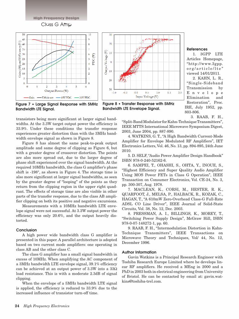
5MHz Bandwidth Large Signal ResponseThe LTE standard has a number of signal bandwidths
between 1.4MHz and 20MHz. The measurements carried out in the previous section were repeated with a 5MHz bandwidth LTE envelope signal. Assuming the envelope amplifier must have a bandwidth twice that of the RF signal for accurate reproduction, then the class G ampli-fier should be sufficient. The large signal response with a swept input signal power is shown in Figure 7.
With respect to Figure 5, the current consumption when the 5MHz bandwidth envelope signal is used is greater. This is possibly due to the turn-off time of the
Figure 4 • Small Signal Response of Class G Amplifier.
Figure 5 • Large Signal Response with 3MHz Bandwidth LTE Signal.
Figure 6 • Transfer Response with 3MHz Bandwidth LTE Envelope Signal.
24 High Frequency Electronics
High Frequency Design
Class G Amp
transistors being more significant at larger signal band-widths. At the 3.3W target output power the efficiency is 33.9%. Under these conditions the transfer response experiences greater distortion than with the 3MHz band-width envelope signal as shown in Figure 8.
Figure 8 has almost the same peak-to-peak output amplitude and same degree of clipping as Figure 6, but with a greater degree of crossover distortion. The points are also more spread out, due to the larger degree of phase shift experienced over the signal bandwidth. At the required 10MHz bandwidth, the class G amplifier’s phase shift is -198°, as shown in Figure 4. The storage time is also more significant at larger signal bandwidths, as seen by the greater degree of “looping” of the points as they return from the clipping region in the upper right quad-rant. The effects of storage time are also visible in other parts of the transfer response, due to the class AB ampli-fier clipping on both its positive and negative excursions.
Measurements with a 10MHz bandwidth LTE enve-lope signal were not successful. At 3.3W output power the efficiency was only 20.6%, and the output heavily dis-torted.
ConclusionA high power wide bandwidth class G amplifier is
presented in this paper. A parallel architecture is adopted based on two current mode amplifiers: one operating in class AB and the other class C.
The class G amplifier has a small signal bandwidth in excess of 10MHz. When amplifying the AC component of a 3MHz bandwidth LTE envelope signal, 39.1% efficiency can be achieved at an output power of 3.3W into a 33Ω load resistance. This is with a moderate 2.3dB of signal clipping.
When the envelope of a 5MHz bandwidth LTE signal is applied, the efficiency is reduced to 33.9% due to the increased influence of transistor turn-off time.
References1. 3GPP LTE
Articles Homepage, “http://www.3gpp.o r g / a r t i c l e / l t e ” viewed 14/01/2011.
2. KAHN, L. R., “Single-Sideband Transmission by E n v e l o p e Elimination and Restoration”, Proc.
IRE, July 1952, pp. 803-806.
3. RAAB, F. H., “Split-Band Modulator for Kahn-Technique Transmitters”, IEEE MTTS International Microwave Symposium Digest, 2003, June 2004, pp. 887-890.
4. WATKINS, G. T., “A High Bandwidth Current-Mode Amplifier for Envelope Modulated RF Amplifiers”, IET Electronics Letters, Vol. 46, No. 13, pp. 894-895, 24th June 2010.
5. D. SELF, “Audio Power Amplifier Design Handbook” ISBN 978-0-240-52162-6.
6. SAMPEI, T., OHASHI, S., OHTA, Y., INOUE, S., “Highest Efficiency and Super Quality Audio Amplifier Using MOS Power FETs in Class G Operation”, IEEE Transaction on Consumer Electronics, Vol. CE-24, No. 3, pp. 300-307, Aug. 1978.
7. MACLEAN, K., CORSI, M., HESTER, R. K., QUARFOOT, J., MELSA, P., HALBACK, R., KOZAK, C., HAGAN, T., “A 610mW Zero-Overhead Class-G Full-Rate ADSL CO Line Driver”, IEEE Journal of Solid-State Circuits, Vol. 38, No. 12, Dec. 2003.
8. PRESSMAN, A. I., BILLINGS, K., MOREY, T., “Switching Power Supply Design”, McGraw Hill, ISBN 978-0-07-148272-1, pp. 60.
9. RAAB, F. H., “Intermodulation Distortion in Kahn-Technique Transmitters”, IEEE Transactions on Microwave Theory and Techniques, Vol/ 44, No. 12, December 1996.
Author InformationGavin Watkins is a Principal Research Engineer with
Toshiba Research Europe Limited where he develops lin-ear RF amplifiers. He received a MEng in 2000 and a PhD in 2003 both in electrical engineering from University of Bristol. He can be contacted by email at: [email protected].
Figure 7 • Large Signal Response with 5MHz Bandwidth LTE Signal.
Figure 8 • Transfer Response with 5MHz Bandwidth LTE Envelope Signal.