A Hands-on Introduction to Nanoscience: Microfabrication Microfabrication... that's how.
45
A Hands-on Introduction to Nanoscience: www.virlab.virginia.edu/Nanoscience_class/Nanoscience_class.htm Microfabrication Microfabrication . . . that's how you make integrated circuits, right?
-
Upload
kenia-roope -
Category
Documents
-
view
251 -
download
1
Transcript of A Hands-on Introduction to Nanoscience: Microfabrication Microfabrication... that's how.

A Hands-on Introduction to Nanoscience: www.virlab.virginia.edu/Nanoscience_class/Nanoscience_class.htm
Microfabrication
Microfabrication . . . that's how you make integrated circuits, right?

A Hands-on Introduction to Nanoscience: www.virlab.virginia.edu/Nanoscience_class/Nanoscience_class.htm
It's now about a lot more, including "Micro-electro-mechanical Systems (MEMS)
This and images to follow are "Courtesy of Sandia National Laboratories,SUMMiTTM Technologies, www.mems.sandia.gov"
Images were found at http://mems.sandia.gov/scripts/images.asp
Multiple Gear Speed Reduction Unit

A Hands-on Introduction to Nanoscience: www.virlab.virginia.edu/Nanoscience_class/Nanoscience_class.htm
Alignment Clip
Used in conjunction with a transmission to maintain the alignment of the two layers of gears
This complex device is entirely batch-fabricated, with no assembly required
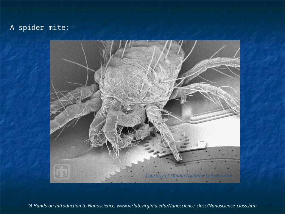
But How Big is This?
Sandia did not include scale markers
I'd guess layers are ~ 0.1 um thick
For scale they did include this:
Courtesy of Sandia National Laboratories
"A Hands-on Introduction to Nanoscience: www.virlab.virginia.edu/Nanoscience_class/Nanoscience_class.htm
A spider mite:
Courtesy of Sandia National Laboratories

What else can you make?How about a steam engine?
Triple-Piston Microsteam Engine
In a humid environment, water condenses inside three open ended cylinders.
It is then heated by electric current passing through adjacent wire.
The water vaporizes, its expansion pushing the pistons out.
Once steam bubbles burst, capillary forces then pull pistons back into cylinders (etc.).
Courtesy of Sandia National Laboratories

A Hands-on Introduction to Nanoscience: www.virlab.virginia.edu/Nanoscience_class/Nanoscience_class.htm
Or a ratchet indexing motor:
Courtesy of Sandia National Laboratories
Courtesy of Sandia National Laboratories
With side to side motion of frame likely
provided by steam engine of previous slide

A Hands-on Introduction to Nanoscience: www.virlab.virginia.edu/Nanoscience_class/Nanoscience_class.htm
Which can be used for . . . revenge!
Spider mites helping to demonstrate motor:
Actuator (here possibly electrostatic) at top
Driving ratchet and pawl on gear
Yielding a "mite go round"
The spider mite really giving motor a work out:
Courtesy of Sandia National Laboratories
Supporting webpage with embedded animations:Microfabrication - Supporting Materials - Animations_1_2
A Hands-on Introduction to Nanoscience: www.virlab.virginia.edu/Nanoscience_class/Nanoscience_class.htm
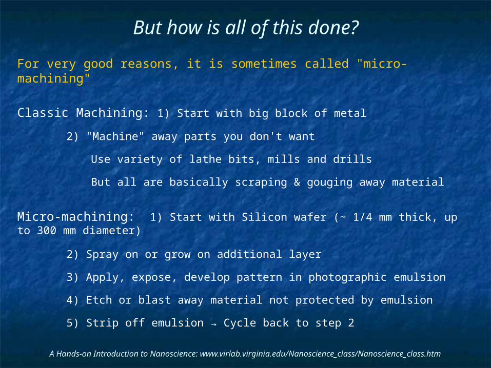
But how is all of this done?
For very good reasons, it is sometimes called "micro-machining"
Classic Machining: 1) Start with big block of metal
2) "Machine" away parts you don't want
Use variety of lathe bits, mills and drills
But all are basically scraping & gouging away material
Micro-machining: 1) Start with Silicon wafer (~ 1/4 mm thick, up to 300 mm diameter)
2) Spray on or grow on additional layer
3) Apply, expose, develop pattern in photographic emulsion
4) Etch or blast away material not protected by emulsion
5) Strip off emulsion → Cycle back to step 2

A Hands-on Introduction to Nanoscience: www.virlab.virginia.edu/Nanoscience_class/Nanoscience_class.htm
Schematically:
:Starting substrate
:Deposit layer of desired material
Deposit photographic emulsion:
Expose photographic emulsion:
A Hands-on Introduction to Nanoscience: www.virlab.virginia.edu/Nanoscience_class/Nanoscience_class.htm
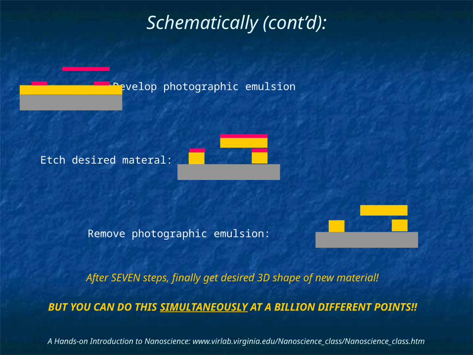
Schematically (cont’d):
:Develop photographic emulsion
Etch desired materal:
Remove photographic emulsion:
After SEVEN steps, finally get desired 3D shape of new material!
BUT YOU CAN DO THIS SIMULTANEOUSLY AT A BILLION DIFFERENT POINTS!!

A Hands-on Introduction to Nanoscience: www.virlab.virginia.edu/Nanoscience_class/Nanoscience_class.htm
Or going over that a little more slowly:Step 1) Start with Silicon wafer
Silicon, element 14 in the periodic table, is known as a semiconductor:
- Insulators: Electrons held so strongly in bonds they can't move around
- Conductors (metals): Electron bonds so weak, electrons wander everywhere
- Semiconductor: Electrons can escape bonds (w/ heat) or
Extra non-bonding electrons can be added via impurity atoms
For details see "UVA Virtual Lab" webpage on How Semiconductors and Transistors Work
A Hands-on Introduction to Nanoscience: www.virlab.virginia.edu/Nanoscience_class/Nanoscience_class.htm
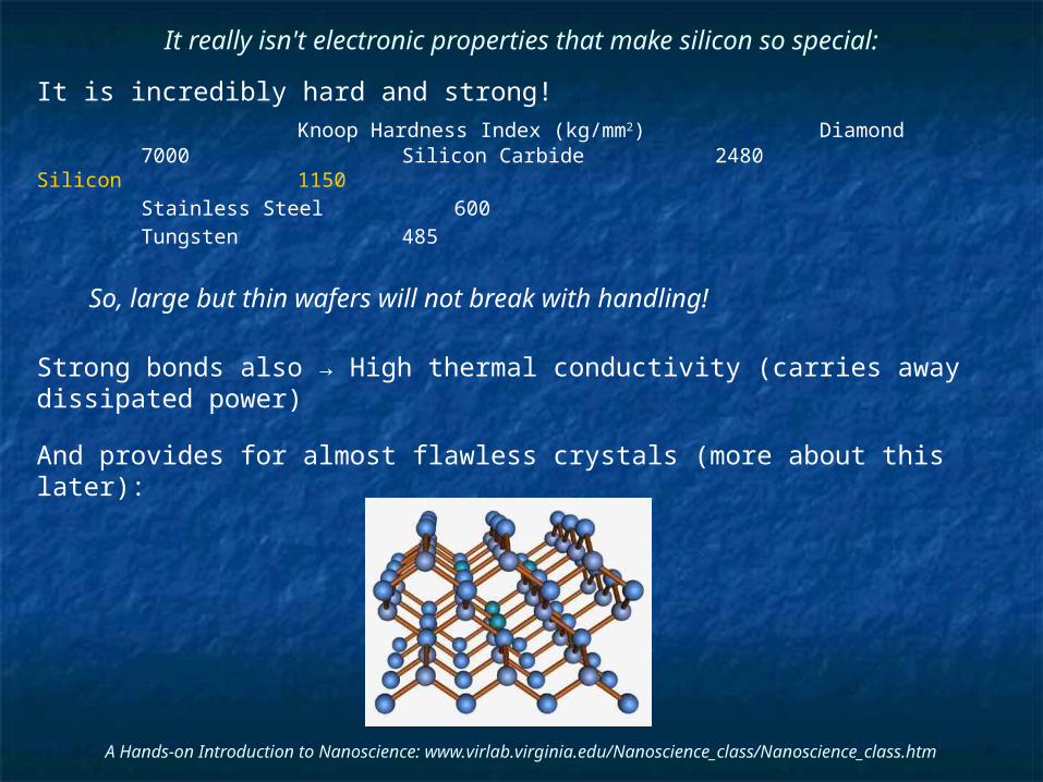
It really isn't electronic properties that make silicon so special:
It is incredibly hard and strong! Knoop Hardness Index (kg/mm2)
Diamond 7000Silicon Carbide 2480Silicon 1150
Stainless Steel 600Tungsten 485
So, large but thin wafers will not break with handling!
Strong bonds also → High thermal conductivity (carries away dissipated power)
And provides for almost flawless crystals (more about this later):

A (significant) digression pertaining to Silicon:
It is pronounced (in the U.S. Pacific Coast dialect) as "sil-ah-cun"
Similar to state of Oregon which is pronounced "Or-ah-gun"
Reasons for using this pronunciation:
1) N. California IS the birthplace and spiritual center of the associated industry
2) Silicone (common mispronunciation of silicon) is VERY different:
Silicone (a.k.a. "siloxane"):
- Strongly cross-linked => Rubber w/ exceptional heat and chemical resistance
- More weakly cross-linked + H2O => Silicone Gel (of breast implant fame)
- Change H's to methyl groups => Polydimethylsiloxane ("PDMS")
OSiH
H
OSiH
H
OSiH
H
(from Wikipedia webpage on silicon dioxide)
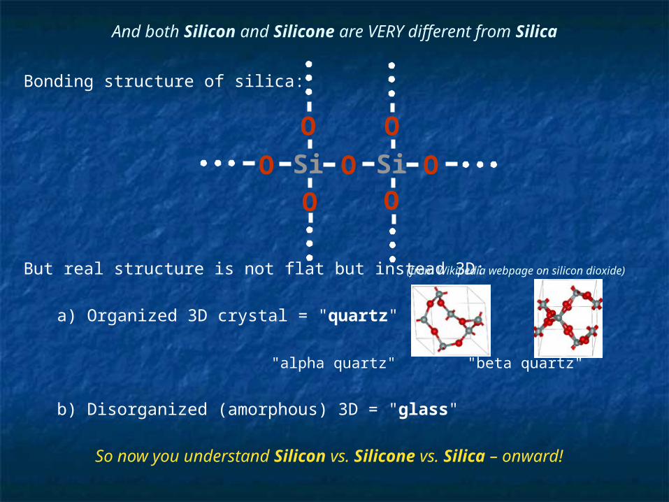
And both Silicon and Silicone are VERY different from Silica
Bonding structure of silica:
But real structure is not flat but instead 3D:
a) Organized 3D crystal = "quartz"
"alpha quartz" "beta quartz"
b) Disorganized (amorphous) 3D = "glass"
So now you understand Silicon vs. Silicone vs. Silica – onward!
SiO
O
OSiOO
O
O
A Hands-on Introduction to Nanoscience: www.virlab.virginia.edu/Nanoscience_class/Nanoscience_class.htm
Step 2) Spray on or grow on additional layer
Alternative i) Spray via evaporation:
Heat up the material you want to deposit until it starts to fall apart
Do this in a vacuum so that what comes off goes in straight line and doesn't react with anything in-flight
However doesn't work for many materials that don't come apart as compounds
Example SiO2 (solid) → SiO (vapor) + 1/2 O2
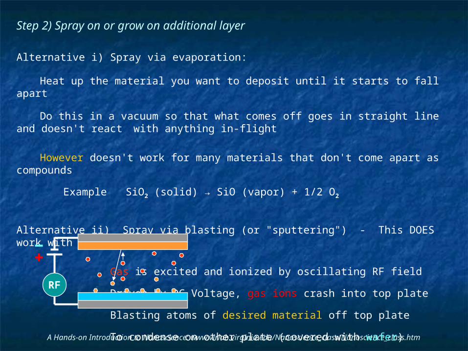
Alternative ii) Spray via blasting (or "sputtering") - This DOES work with compounds!
Gas is excited and ionized by oscillating RF field
Driven by DC Voltage, gas ions crash into top plate
Blasting atoms of desired material off top plate
To condense on other plate (covered with wafer)
RF
A Hands-on Introduction to Nanoscience: www.virlab.virginia.edu/Nanoscience_class/Nanoscience_class.htm
Alternative iii) "Grow" a layer of what you want via surface chemical reactions
Sort of like rusting iron: 2 Fe (solid) + 3/2 O2 (gas) → Fe2O3 (solid)
Except that where iron oxide is a crumbly porous mess,
Silicon oxide is . . . glass! Si (solid) + 1/2 O2 (gas) → SiO2 (solid)
Chemically, glass in incredibly tough
In what do chemists use to store almost ALL of their chemicals?
(Can almost count exceptions on one hand: HF, KOH . . .)
Although brittle, it is mechanically strong: "fiber-glass" reinforced . . ."
Can also "Grow" via gas phase chemical reactions:
SiH4 + O2 → SiO2 (solid) + 2 H2 (Disclaimer: Goes "boom" if don't carefully dilute!!)
And works for other related insulators
3 SiH4 + 4 NH4 → Si3N4 (solid) + 14 H2
A Hands-on Introduction to Nanoscience: www.virlab.virginia.edu/Nanoscience_class/Nanoscience_class.htm
Step 3) Apply, expose, develop pattern in photographic emulsion
Emulsion is also called "resist" because we want it to resist etching
OK, after glass, what is chemist's second choice for chemical container?
(HINT: Advice given to Dustin Hoffman's character in movie The Graduate -1967)
A "cross-linked" polymer (here "vulcanized" rubber)
Hydrocarbon monomers (lone carbon-based chains) can be very chemically resistant
Are here held together by the sulfur atoms - But sulfur linking is induced by heat not light!!
This and figures to follow are from Professor R. Bruce Darling's superb notes for EE-527 - Microfabrication, at the University of Washington
A link to his class website and cached copies of his class lecture note can be found at:
Microfabrication - Supporting Materials - Darling

A Hands-on Introduction to Nanoscience: www.virlab.virginia.edu/Nanoscience_class/Nanoscience_class.htm
So you need different LIGHT stimulated way of linking/unlinking monomers
One way (used in Kodak's KTFR, workhorse of the early integrated circuits):
2,6-bis(4-azidobenzal)-4-methylcyclohexanone or just "ABC" (I didn't make this up!)
Light reacts with "azide" NH3 end units, converting them to reactive radicals
So that they chain themselves to other monomers ("cross-linking" them):
Unlinked | Linked | Unlinked
Source: R. Bruce Darling
University of Washington
Source: R. Bruce Darling
University of Washington
UV LIGHT

A Hands-on Introduction to Nanoscience: www.virlab.virginia.edu/Nanoscience_class/Nanoscience_class.htm
Modern "photoresists" use different chemical mixtures and different tricks:
Phenolic "resin" (monomer):
PLUS photoactive compound (PAC) that light switches from hydrophobic to philic
Where not struck by light →
Sheds water-based remover
(and thus everything stays put)
Where hit by light, sucks in
water-based remover (which removes all)
Source: R. Bruce Darling
University of Washington
Source: R. Bruce Darling
University of Washington

A Hands-on Introduction to Nanoscience: www.virlab.virginia.edu/Nanoscience_class/Nanoscience_class.htm
Apply this "resist" to the wafer by spinning it on:
Then expose pattern through photographic shadow "mask (also called a "reticle"):"
Source: R. Bruce Darling
University of Washington
Source: R. Bruce Darling
University of Washington

A Hands-on Introduction to Nanoscience: www.virlab.virginia.edu/Nanoscience_class/Nanoscience_class.htm
Actually done in a tool called a “mask aligner” which (in older non-automated versions):
- Uses microscope allowing you to first position the resist covered wafer below the mask
- In “contact” machine, it then clamps resist/wafer tightly against mask
UV light then passes through transparent regions of mask onto resist/wafer
- In “projection” machine, shadow image of mask is de-magnified and projected onto resist/wafer at perhaps 1/5 original mask size.
- Wafer is then released, “stepped” to new position, and a new area exposed
Source: R. Bruce Darling
University of Washington

A Hands-on Introduction to Nanoscience: www.virlab.virginia.edu/Nanoscience_class/Nanoscience_class.htm
Step 4) Etch or blast away material not protected by emulsion
StripEtch Resist
But can also get fancy and use multiple layers and multiple etches:
Etch 1 Etch 2
StripResist
End up with a sort of diving board like structure:

A Hands-on Introduction to Nanoscience: www.virlab.virginia.edu/Nanoscience_class/Nanoscience_class.htm
What if "diving board" were metallic (or covered by metal)?
And you then applied suitable voltages:
And tried bouncing a laser off a whole bunch of these:
Remember: all "diving boards"
made SIMULTANEOUSLY
What would you get? Hints: 1) I talked about this technology in lecture 1
2) We MAY be using it at this very moment
A Hands-on Introduction to Nanoscience: www.virlab.virginia.edu/Nanoscience_class/Nanoscience_class.htm
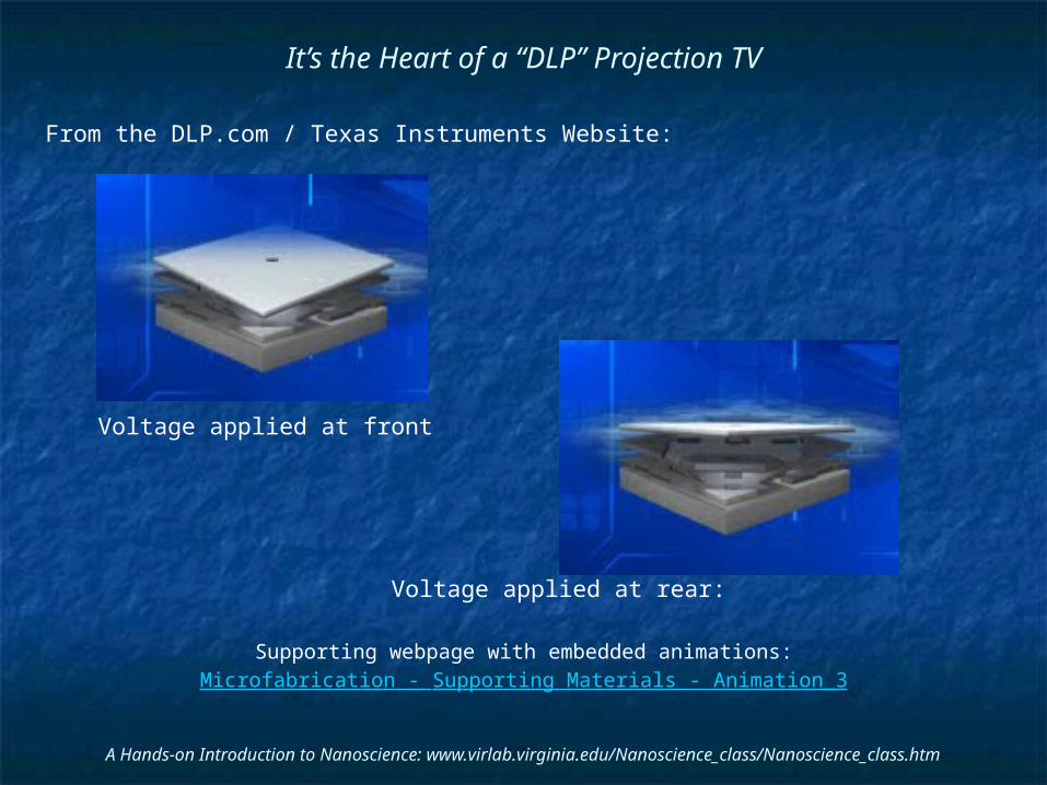
It’s the Heart of a “DLP” Projection TV
From the DLP.com / Texas Instruments Website:
Voltage applied at front
Voltage applied at rear:
Supporting webpage with embedded animations:Microfabrication - Supporting Materials - Animation_3

Here is a more detailed look at two pixels in the device:
KEY POINT: Pieces were not made and brought together to yield this assembly!
INSTEAD: Uniform layer was deposited, photoresist pattern exposed and developed.
Pattern protected parts of layer against removal (transferring pattern to layer).
Then steps were repeated over and over again to build up structure
And this was done, simultaneously, at millions of different points!
(Image found on a Japanese language blog – original probably
from TI.com)

A Hands-on Introduction to Nanoscience: www.virlab.virginia.edu/Nanoscience_class/Nanoscience_class.htm
Comparing schematic with direct SEM image:
("Nanomechanical characterization of multilayer thin film structures for digital micromirror devices," Wei, Bhushan and Jacobs, Ultramicroscopy 100(3-4), pp. 375-389 (2004))
See how the whole thing is made up of layer upon layer upon layer?
(Note: Drawing at left shows mirror up on post not seen in SEM image of real structure at right. Missing or does real device just use understructure as mirror?)
A Hands-on Introduction to Nanoscience: www.virlab.virginia.edu/Nanoscience_class/Nanoscience_class.htm
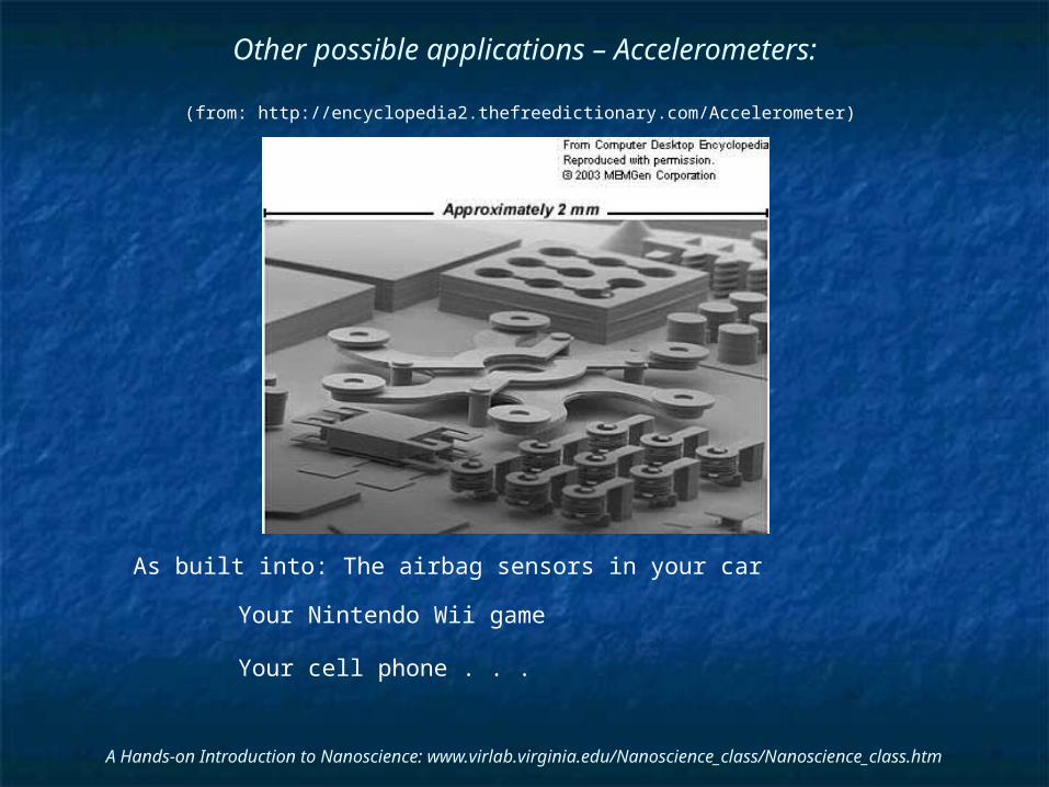
Other possible applications – Accelerometers:
(from: http://encyclopedia2.thefreedictionary.com/Accelerometer)
As built into: The airbag sensors in your car
Your Nintendo Wii game
Your cell phone . . .
A Hands-on Introduction to Nanoscience: www.virlab.virginia.edu/Nanoscience_class/Nanoscience_class.htm
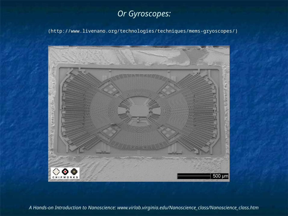
Or Gyroscopes:
(http://www.livenano.org/technologies/techniques/mems-gryoscopes/)
A Hands-on Introduction to Nanoscience: www.virlab.virginia.edu/Nanoscience_class/Nanoscience_class.htm
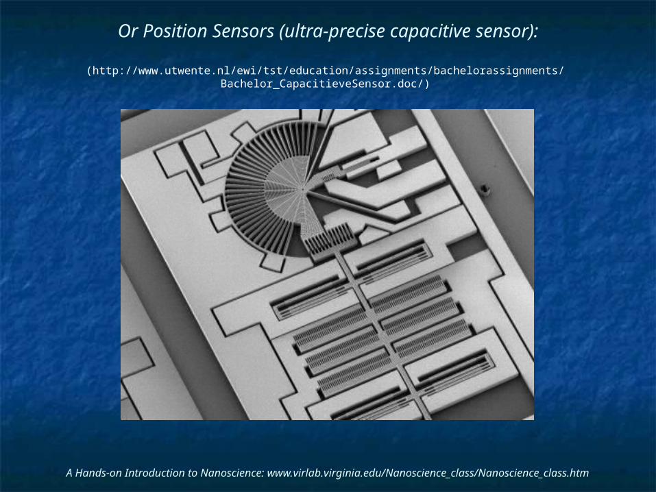
Or Position Sensors (ultra-precise capacitive sensor):
(http://www.utwente.nl/ewi/tst/education/assignments/bachelorassignments/Bachelor_CapacitieveSensor.doc/)

And eventually, maybe even a Microchip DNA Sequencer:
The Dream:
Separate DNA into single strands
Draw ONE strand through a nanopore by applying positive voltage below
Sense what type of base is passing through pore at given moment
For instance, by putting complementary bases (A, T, C or G) to sides of nanopore (right)
(www.nature.com/nnano/journal/v6/n10/full/nnano.2011.129.html?WT.ec_id=NNANO-201110)
(http://researchmatters.asu.edu/stories/race-develop-cheap-rapid-dna-sequencing-753)

How far they have gotten to date:
(http://www.nanoporetech.com/technology/introduction-to-nanopore-sensing/introduction-to-nanopore-sensing)
Protein-based DNA separator / nanopores embedded in membrane (left)
Which can discriminate between different types of molecules based on electrical current (right)
And can distinguish between DNA having all one base or all another base (e.g. all A vs. all T)
Further, did see one report of being able to identify AAA vs. TTT triplet sequences
But not yet able to identify individual bases in an arbitrary sequence
And not yet able to mass produce via microfabrication

A Hands-on Introduction to Nanoscience: www.virlab.virginia.edu/Nanoscience_class/Nanoscience_class.htm
And let's not forget microfabrication's original and still biggest application
Transistors in Integrated Circuits:
The complete depiction (fourteen 3D animated scenes!) including deposition of all layers, patterning via four photo-masking steps, and etching can be viewed at the “UVA Virtual Lab” webpage on “How Integrated Circuits are Made:”
www.virlab.virginia.edu/VL/IC_process.htm

A Hands-on Introduction to Nanoscience: www.virlab.virginia.edu/Nanoscience_class/Nanoscience_class.htm
But how exactly do they make those more mechanical (MEMS) things?
I've searched and searched for full pictorial description of MEMS process – and failed
Reason #1) To this point, most people doing MEMS got started building integrated circuits
Which is already well depicted in many textbooks (and on my website)
So they now use a sort of pictorial shorthand that leaves out most of the steps
Correctly assuming that others with similar training can figure it out for themselves
Reason #2) It is EXTREMELY hard to create complete drawings of process
New layers naturally conform with shape of patterned layers already there
But CAD/animation tools don't have a "deposit conformal layer" button
So you have to draw conformal layer as sum of huge number of sub shapes
As I DID (painfully) in transistor animation linked to in preceding slide!

A Hands-on Introduction to Nanoscience: www.virlab.virginia.edu/Nanoscience_class/Nanoscience_class.htm
But here is one depiction giving start to finish process of making gears:
Even though it does still jump forward 5-10 steps between images
Source: Prof. LaVern Starman, Wright State Universityhttp://www.cs.wright.edu/people/faculty/kxue/mems/MEMS_3FabricationM06.pdf
On a substrate (likely a Si wafer with capping layers) deposit layer of polycrystalline Si (baby blue). Then deposit and pattern a photoresist layer (red):
Deposit and pattern a thick oxide layer (pale purple):
A Hands-on Introduction to Nanoscience: www.virlab.virginia.edu/Nanoscience_class/Nanoscience_class.htm
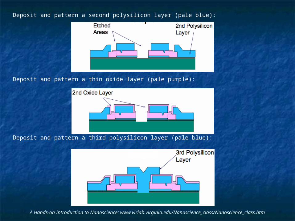
Deposit and pattern a second polysilicon layer (pale blue):
Deposit and pattern a thin oxide layer (pale purple):
Deposit and pattern a third polysilicon layer (pale blue):
A Hands-on Introduction to Nanoscience: www.virlab.virginia.edu/Nanoscience_class/Nanoscience_class.htm
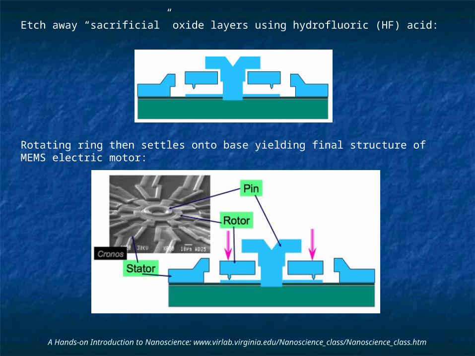
Etch away “sacrificial” oxide layers using hydrofluoric (HF) acid:
Rotating ring then settles onto base yielding final structure of MEMS electric motor:
A Hands-on Introduction to Nanoscience: www.virlab.virginia.edu/Nanoscience_class/Nanoscience_class.htm
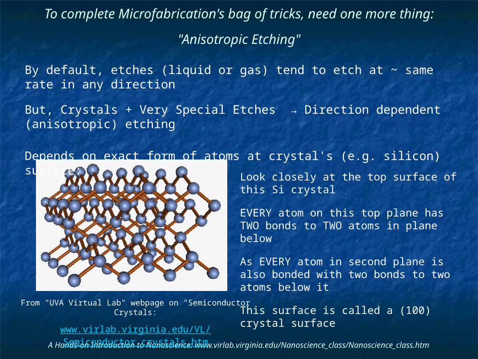
To complete Microfabrication's bag of tricks, need one more thing:
"Anisotropic Etching"
Look closely at the top surface of this Si crystal
EVERY atom on this top plane has TWO bonds to TWO atoms in plane below
As EVERY atom in second plane is also bonded with two bonds to two atoms below it
This surface is called a (100) crystal surface
By default, etches (liquid or gas) tend to etch at ~ same rate in any direction
But, Crystals + Very Special Etches → Direction dependent (anisotropic) etching
Depends on exact form of atoms at crystal's (e.g. silicon) surface:
From "UVA Virtual Lab" webpage on "Semiconductor Crystals:
www.virlab.virginia.edu/VL/Semiconductor_crystals.htm
A Hands-on Introduction to Nanoscience: www.virlab.virginia.edu/Nanoscience_class/Nanoscience_class.htm
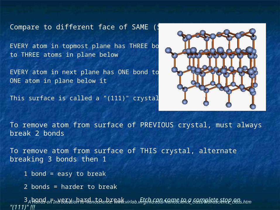
Compare to different face of SAME (Si) crystal:
EVERY atom in topmost plane has THREE bondsto THREE atoms in plane below
EVERY atom in next plane has ONE bond to ONE atom in plane below it
This surface is called a "(111)" crystal surface
To remove atom from surface of PREVIOUS crystal, must always break 2 bonds
To remove atom from surface of THIS crystal, alternate breaking 3 bonds then 1
1 bond = easy to break
2 bonds = harder to break
3 bond = very hard to break Etch can come to a complete stop on "(111)" !!!

A Hands-on Introduction to Nanoscience: www.virlab.virginia.edu/Nanoscience_class/Nanoscience_class.htm
Normal vs. Anisotropic Etch:
Normal (isotropic) : Anisotropic:
Anisotropic etched surface develops (111) facets !!!

A Hands-on Introduction to Nanoscience: www.virlab.virginia.edu/Nanoscience_class/Nanoscience_class.htm
And this opens a very wide door:
Start with square hole in masking layer → Pyramidal pit in silicon
But start with irregularly mask hole and STILL etch silicon toward pyramidal pit
Chews up random surfaces quickly, then collides with (111) surface planes!
Figures again from Professor R. Bruce Darling's Microfabrication Notes - University of Washington http://www.ee.washington.edu/research/microtech/cam/PROCESSES/NEWtutorial.html

A Hands-on Introduction to Nanoscience: www.virlab.virginia.edu/Nanoscience_class/Nanoscience_class.htm
Or to make (nearly) free-standing structures:
Start with "U" shaped hole in masking layer:
First - Faceted trench in Si
Trenches begin to undercut mask
Finally part of mask left free-standing
Diving board over swimming pool!
Source: R. Bruce Darling
University of Washington

Or if leave islands of masking layer on top of the silicon:
Yielding almost atomically sharp Si cantilever assemblies YOU will use with this class's Atomic Force Microscopes !!
Entire object at bottom is “micro-machined" from single piece of silicon
Its' hugely exaggerated in size, largest dimension actually ~ 3mm
From UVA "Virtual Lab" webpage on "Atomic Force Microscope"
www.virlab.virginia.edu/VL/easyScan_AFM.htm

A Hands-on Introduction to Nanoscience: www.virlab.virginia.edu/Nanoscience_class/Nanoscience_class.htm
Or similar techniques used by Prof. Michael Reed here at UVA to make:
He sticks these things inside people!
(to repair arteries, stitch tissue together . . .)

A Hands-on Introduction to Nanoscience: www.virlab.virginia.edu/Nanoscience_class/Nanoscience_class.htm
An incredibly powerful precursor to nanotechnology
Cheap fast way of simultaneously making BILLIONS of micro things
Not something that will be easily surpassed!!
Probably an essential tool in inducing nanoscale self-assembly (later classes)
Likely an ultimate partner with nanotechnology
as future devices combine both technologies, one atop another,
exploiting what each does best
All of these tricks and capabilities make Microfabrication:
A Hands-on Introduction to Nanoscience: www.virlab.virginia.edu/Nanoscience_class/Nanoscience_class.htm
Credits / Acknowledgements
Funding for this class was obtained from the National Science Foundation (under their Nanoscience Undergraduate Education program) and from the University of Virginia.
This set of notes was authored by John C. Bean who also created all figures not explicitly credited above.
Many of those figures (and much of the material to be used for this class) are drawn from the "UVA Virtual Lab" (www.virlab.virginia.edu) website developed under earlier NSF grants.
Copyright John C. Bean (2015)
(However, permission is granted for use by individual instructors in non-profit academic institutions)