A Fully Digital Hysteresis Current Controller for AnActive Power Filter
30
A Fully Digital Hysteresis Current Controller for an Active Power Filter David M.E. Ingram and Simon D. Round Department of Electrical & Electronic Engineering University of Canterbury Private Bag 4800 Christchurch, New Zealand Abstract An active power filter is used to eliminate current harmonics produced by non- linear loads. This paper discusses a fully digital method of controlling a power inverter used to inject the active filter compensating currents into the power system. A digital signal processor performs the harmonic isolation and generates a digital reference current. A hysteresis current controller has been implemented in a field programmable gate array that generates the inverter switching signals using this reference. This reduces the analogue circuitry and enhances the system’s immunity to EMI. The performance of a small-scale inverter under completely digital control is presented and discussed.
-
Upload
ahmed-helmy -
Category
Documents
-
view
37 -
download
7
Transcript of A Fully Digital Hysteresis Current Controller for AnActive Power Filter
A Fully Digital Hysteresis Current Controller for an
Active Power Filter
David M.E. Ingram and Simon D. Round
Department of Electrical & Electronic Engineering
University of Canterbury
Private Bag 4800
Christchurch, New Zealand
Abstract An active power filter is used to eliminate current harmonics produced by non-
linear loads. This paper discusses a fully digital method of controlling a power inverter used
to inject the active filter compensating currents into the power system. A digital signal
processor performs the harmonic isolation and generates a digital reference current. A
hysteresis current controller has been implemented in a field programmable gate array that
generates the inverter switching signals using this reference. This reduces the analogue
circuitry and enhances the system’s immunity to EMI. The performance of a small-scale
inverter under completely digital control is presented and discussed.
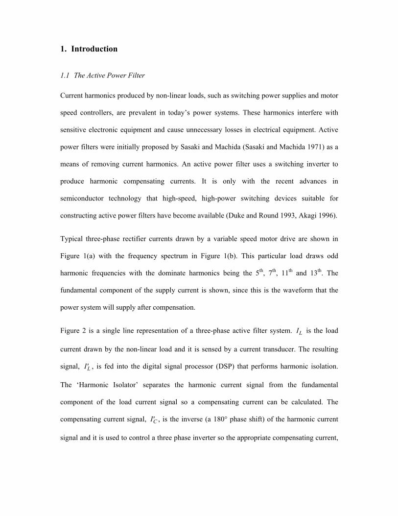
1. Introduction
1.1 The Active Power Filter
Current harmonics produced by non-linear loads, such as switching power supplies and motor
speed controllers, are prevalent in today’s power systems. These harmonics interfere with
sensitive electronic equipment and cause unnecessary losses in electrical equipment. Active
power filters were initially proposed by Sasaki and Machida (Sasaki and Machida 1971) as a
means of removing current harmonics. An active power filter uses a switching inverter to
produce harmonic compensating currents. It is only with the recent advances in
semiconductor technology that high-speed, high-power switching devices suitable for
constructing active power filters have become available (Duke and Round 1993, Akagi 1996).
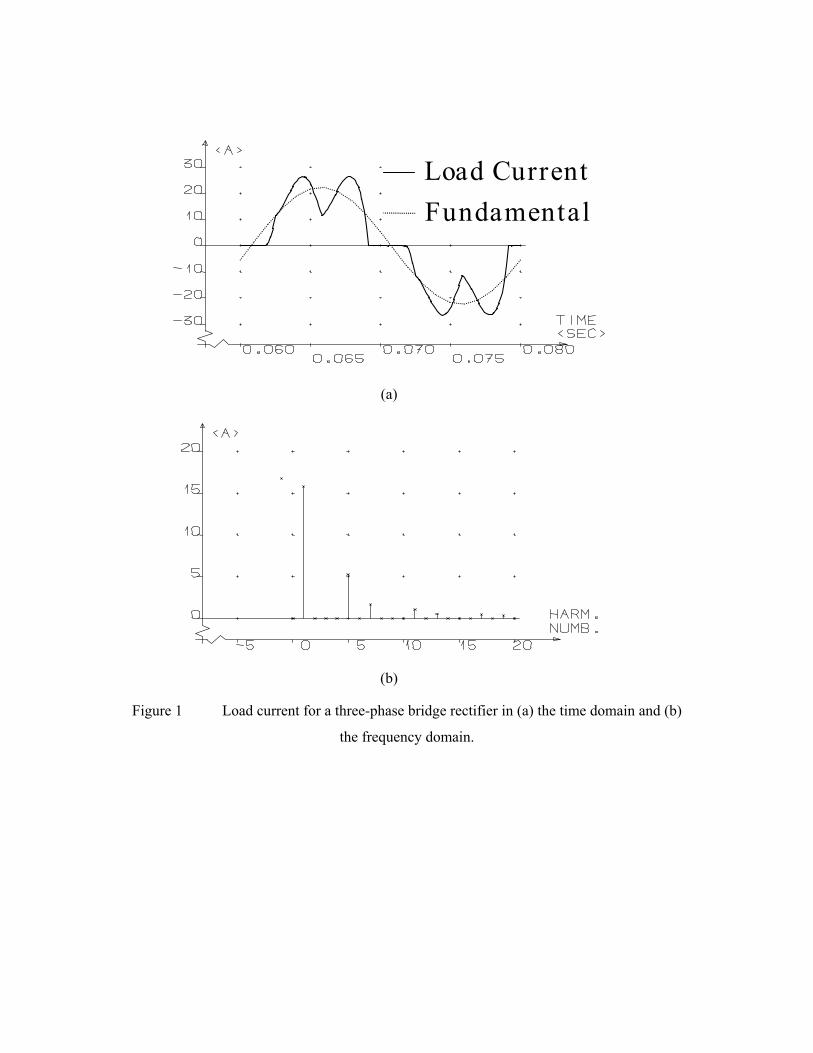
Typical three-phase rectifier currents drawn by a variable speed motor drive are shown in
Figure 1(a) with the frequency spectrum in Figure 1(b). This particular load draws odd
harmonic frequencies with the dominate harmonics being the 5th, 7th, 11th and 13th. The
fundamental component of the supply current is shown, since this is the waveform that the
power system will supply after compensation.
Figure 2 is a single line representation of a three-phase active filter system. IL is the load
current drawn by the non-linear load and it is sensed by a current transducer. The resulting
signal, ′IL , is fed into the digital signal processor (DSP) that performs harmonic isolation.
The ‘Harmonic Isolator’ separates the harmonic current signal from the fundamental
component of the load current signal so a compensating current can be calculated. The
compensating current signal, ′IC , is the inverse (a 180° phase shift) of the harmonic current
signal and it is used to control a three phase inverter so the appropriate compensating current,
IC , is injected into the power system. This cancels the harmonics drawn by the non-linear
load, leaving the resulting supply current, IS , sinusoidal.
1.2 Hysteresis Current Control
Active filters produce a nearly sinusoidal supply current by measuring the harmonic currents
and then injecting them back into the power system with a 180° phase shift. A controlled
current inverter is required to generate this compensating current. Hysteresis current control is
a method of controlling a voltage source inverter so that an output current is generated which
follows a reference current waveform. This method controls the switches in an inverter
asynchronously to ramp the current through an inductor up and down so that it tracks a
reference current signal. Hysteresis current control is the easiest control method to implement
(Brod and Novotny 1985). One disadvantage is that there is no limit to the switching
frequency, but additional circuitry can be used to limit the maximum switching frequency
(Malesani et al 1996).
A hysteresis current controller is implemented with a closed loop control system and is shown
in diagrammatic form in Figure 3(a). An error signal, e(t), is used to control the switches in an
inverter. This error is the difference between the desired current, iref(t), and the current being
injected by the inverter, iactual(t). When the error reaches an upper limit, the transistors are
switched to force the current down. When the error reaches a lower limit the current is forced
to increase. The minimum and maximum values of the error signal are emin and emax
respectively. The range of the error signal, emax – emin, directly controls the amount of ripple in
the output current from the inverter and this is called the Hysteresis Band. The hysteresis
limits, emin and emax, relate directly to an offset from the reference signal and are referred to as
the Lower Hysteresis Limit and the Upper Hysteresis Limit. The current is forced to stay
within these limits even while the reference current is changing. The ramping of the current
between the two limits is illustrated in Figure 3(b).
The switching frequency is altered by the width of the hysteresis band, the size of the inductor
that the current flows through (L in Figure 3(a)) and the DC voltage applied to the inductor by
the inverter. A larger inductance will yield a smaller didt for a given voltage and so the slope
of the sawtooth waveform in Figure 3(b) will be less.
1.3 Digital Control of Inverter Current
The active filter controller is implemented with a Digital Signal Processor (DSP). All
calculations are made digitally and the desired compensating current is represented
numerically inside the DSP. The power switches in an inverter can either be on or off, and
thus can be considered to be digital. Therefore the inverter controller that interfaces the DSP
to the inverter is ideally suited to be constructed from a digital circuit rather than the more
common analogue implementation. The digital inverter controller calculates the hysteresis
limits mathematically and performs the magnitude comparisons with digital logic. Traditional
hysteresis current controllers perform these functions with analogue operational amplifiers
and comparators. Laying an analogue circuit out on a printed circuit board takes a
considerable amount of time and uses a large number of components, many of which require
fine adjustment. Any changes to the design would result in the procedure being repeated. A
Field Programmable Gate Array (FPGA) is a reprogrammable digital logic integrated circuit
and allows modifications to the inverter controller to be made internally without any changes
to the printed circuit board. An FPGA implementation is very compact because it is a single
component and does not require a large number of support integrated circuits (Retif et al.
1993).
Other digital inverter controllers have been built with a DSP and programmable logic, usually
erasable programmable logic devices (EPLD). One such example is that of Lee et al. (Lee et
al. 1996) where space voltage vector control was implemented with a Texas Instruments
TMS320C31 DSP and an EPLD. Other researchers have implemented a digital hysteresis
current controller using the TMS320C31 DSP (Li et al. 1995). These inverter controllers
operate with a low sampling and/or switching frequency of several kilohertz. This low
switching frequency is not high enough to adequately track the active filter's compensating
currents. A digital hysteresis current controller that can generate a high frequency switching
signal suitable for an active filter by operating with a sampling rate of 260 kHz is presented
and discussed in this paper.
2. Theory
2.1 Active Power Filtering Requirements
Active power filtering imposes design restrictions on the inverter that would not normally be
present in other applications, for example, motor speed control. The main difference between
these two applications is the maximum frequency of the current reference. An active power
filter should at least be able to inject frequencies up to the 20th harmonic and ideally be able
to compensate up to the 50th harmonic.
This high frequency operation limits the size of the injection inductor. When the inductance is
too large the maximum rate of change of current will be too low to track the steep current
changes that occur with high frequencies. The small inductances used mean that the rates of
change of current will be high. High switching frequencies result and this causes large losses
in the semiconductor switches. This also leads to increased levels of electromagnetic
interference and requires very high-speed comparisons of the actual current against the
hysteresis limits (illustrated in Figure 3(b)).
2.2 Injection Inductor
The injection inductor must be small enough so that the injected current di/dt is greater than
that of the reference current (the compensating current signal in the active power filter) for the
injected current to track the reference. If Eqn. (1) describes the reference current at the
highest frequency, the maximum di/dt can then be determined from Eqn. (2).
( ) ( )i t A f t= sin 2π (1)
( )max did t A f= 2π (2)
In order to determine the maximum di/dt of the compensating current the di/dt of each
harmonic component must first calculated from its amplitude and frequency values. The
overall maximum di/dt for the compensating current is therefore the highest individual di/dt.
As an example the harmonic giving the highest di/dt is generally the third for single-phase
rectifiers with capacitive loads, yet is the fifth for three phase rectifiers with inductive or
capacitive loads.
From the standard inductor differential equation an expression for di/dt can be determined and
is given by Eqn. (3) where ∆V is the voltage across the inductor (assuming negligible
resistance).
did t
VL
=∆ (3)
The maximum inductance possible should be used in the inverter to give the lowest average
switching frequency. This in turn reduces electromagnetic interference (EMI) and switching
losses in the inverter. An expression for the maximum useable inductance is given by Eqn.
(4), where VDC is the rail-rail DC voltage on the inverter and vsupply is the instantaneous power
supply voltage.
LV vDC
did t
max =−1
2 supply
Reference(max)
(4)
Brod and Novotny (Brod and Novotny 1985) present an expression for the maximum
switching frequency of a hysteresis controller, and this is given in Eqn. (5), where h is the
hysteresis limit, and so the hysteresis band, ∆I, is equal to 2h.
( )fV
hLswDC
max =9
(5)
2.3 Sampling Frequency
Hysteresis current control requires current feedback. The sensed current is compared to the
hysteresis limits and the result of this comparison is used to control the switches in the
inverter. In an analogue system the comparisons are made continuously and the current will
be forced to stay within the hysteresis band at all times. With a digital controller, events
happen at discrete intervals. The sensed current is digitised and the comparisons are made
digitally. The current information is updated at the sampling frequency of the analogue to
digital converter (ADC) that samples the current feedback. If this sampling frequency is too
low there is a chance that the current will have exceeded the hysteresis limits by the time the
comparison is made.
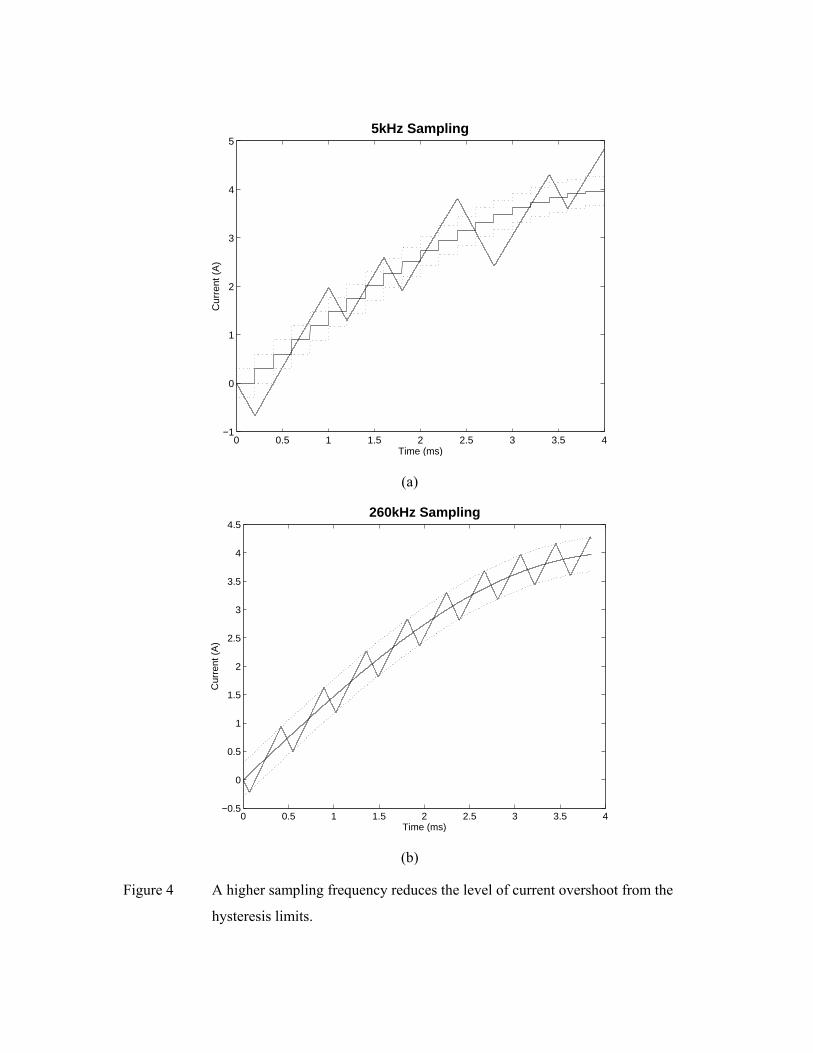
Figure 4 shows the results of a simulated inverter controller with two different sampling
frequencies. The injected current is sampled at 5kHz in (a) and at 260kHz in (b). The
hysteresis band, ∆I, has been set to 0.8A in both cases. It can be seen that the current regularly
exceeds the hysteresis band when the current feedback is sampled too slowly. The reference
and the two hysteresis limits are shown as discrete samples in Figure 4(a) and (b). Once a
switching decision has been made the inverter switches are left unchanged until the next
sample is taken. This new sample is used by the decision logic to determine the next
switching state. The centre solid line in each figure is the current reference and the jagged
solid line is the inverter’s current output. Two dashed lines represent the hysteresis limits
used for the simulation.
Once the injected current travels outside of the hysteresis limits it will continue to do so until
the next sample is taken. It is only at this point that the transistors are set so the current is
ramped in the opposite direction. The high speed sampling of 260kHz gives very good results,
and with only 3.8µs between samples the current will not get far outside the hysteresis limits.
Compare this with the case of 5kHz sampling, where the current is regularly outside of the
hysteresis limits. The time between samples has extended to 200µs, leading to extremely large
current excursions. The minimum sampling frequency needed to achieve an acceptable
overshoot is a function of the injection inductance used and the voltage applied across the
inductance. Each of these affects didt , and therefore the level of current overshoot.
The smaller the injection inductor, the greater the didt , and this will increase the current
overshoot. The worst case is when the current is just inside the hysteresis band when the
comparison is made. The current will then continue on past the limit and will only reverse
direction at the next sampling point. Eqn. (6) gives the maximum current overshoot ∆ iOver for
an inverter with a DC voltage VDC injecting current into an inductance L with a sampling
frequency of fSample, assuming that vSupply = 0. Acceptable current waveforms are achievable by
choosing the sampling frequency so that the overshoot is kept to 5-10% of hysteresis band,
∆I. This keeps the current ripple reasonably close to the design value for a traditional
analogue hysteresis current controller.
∆iVL fOverDC
S am ple=
12 1
(6)
3. Simulation
The operation of the proposed digital hysteresis current controller has been modelled using
Simulink and MATLAB. A single-phase model was developed since the three phases of the
inverter are able to operate independently. A neutral connection is provided and this prevents
the situation arising where the hysteresis band can double due to three phase interactions
(Brod and Novotny 1985).
To get the best possible simulation of a real digital hysteresis current controller the currents
were quantised and sampled. This gives the simulated controller the same dynamic
characteristics as a controller implemented in an FPGA. The hysteresis controller makes
switching decisions based on the reference current signal and the current feedback. The
switching signals are used to control a model of a three-phase inverter that in turn produces a
three-phase voltage output. The voltage is applied across the injection inductor model, which
through the use of differential equations determines the current that flows through the
inductor. This injection current is the output from the simulation and is recorded for further
analysis.
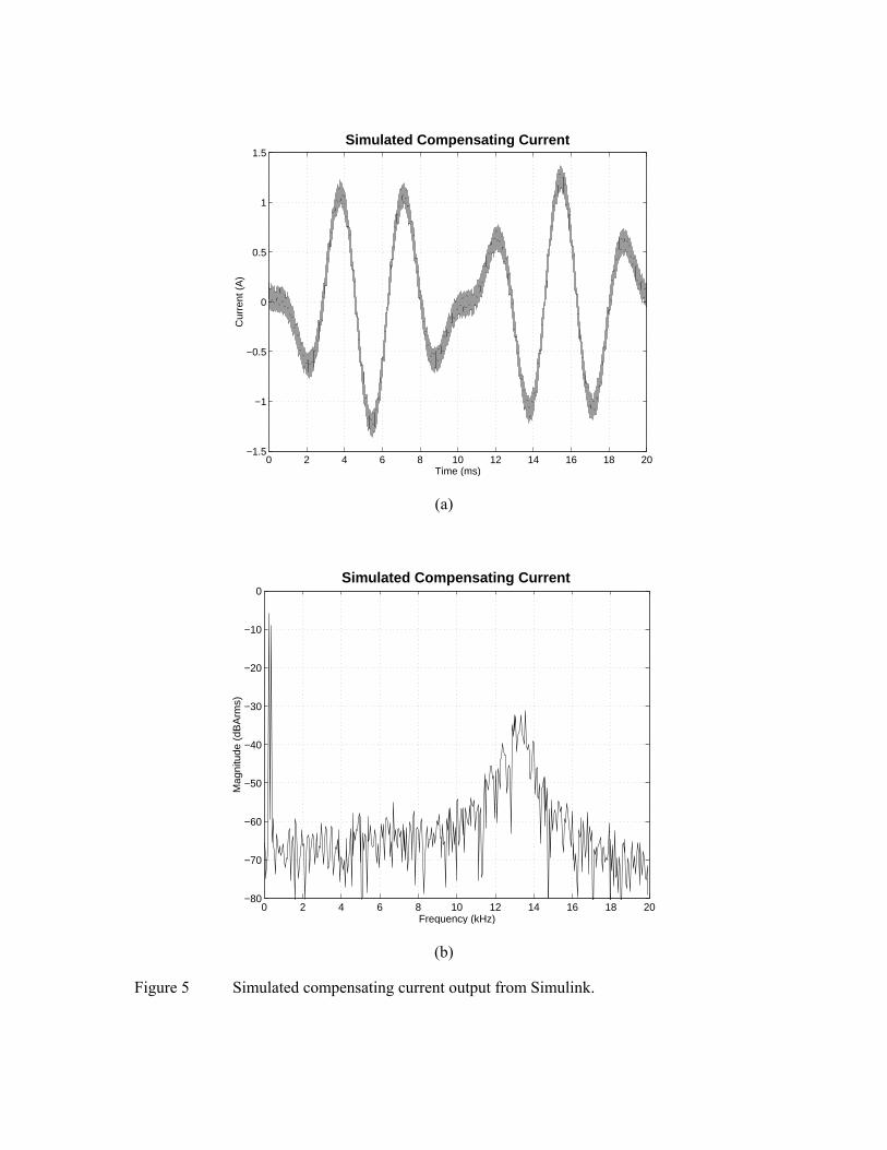
This digital inverter controller is intended for use in an active filter, and so a sample
compensating current, shown in Figure 5(a), was generated. The fundamental frequency is
50Hz and the injection inductance is 4mH. The compensating current is scaled for an overall
load current of 0.71ARMS and the hysteresis band is 0.2A. Figure 5(b) shows the frequency
spectrum of the current in Figure 5(a). The two prominent frequency components at 250Hz
and 350Hz are the harmonics present in the reference signal. The concentration of signal at
13.5kHz is the high frequency switching signal from the inverter. The maximum expected
frequency in the inverter output as calculated by Eqn. (5) is 16.7kHz and this agrees with the
frequency spectrum in Figure 5(b). The unwanted frequency components can be filtered by an
LC low pass filter because they are so far removed from the frequency band of interest, which
is limited to 2.5kHz (50th harmonic at 50 Hz).
4. Inverter Controller Implementation
4.1 System Diagram
The digital inverter controller interfaces the digital signal processor to the three-phase
inverter. Figure 6 shows the inverter system with the controller, the power inverter and
current feedback. A current sensor and transimpedance amplifier convert the high current
output of the inverter to a voltage suitable for digitising by the ADC. The reference current
from the DSP and the digitised injection current are transmitted digitally to the FPGA.
Switching decisions are made by the FPGA that control the output voltage of the inverter. The
voltage applied to the inductor causes a current to flow into or out of the power system.
Figure 7 expands upon the inverter controller, highlighting the internal blocks needed for
hysteresis current control. The controller is completely digital and implemented inside the
FPGA.
4.2 Inverter Controller Parameters
There are a few parameters to be selected for a digital hysteresis controller that are not
required for an analogue controller. Firstly, the resolution of the currents must be specified.
The intended active power filter will be working with load currents up to 400APeak and a
current precision of 0.2A is required. This gives 4000 points over the full scale of the current
(from -400A to +400A). A twelve-bit integer has 4096 possible values and can be used to
represent the load current with the desired precision. The DSP will be working with 12-bit
integers internally and will represent the compensating current as a twelve-bit number. To aid
the comparison of values digitally the current feedback will be digitised with a twelve-bit
analogue to digital converter (ADC).
Secondly, the update frequency of the reference value from the DSP and the sampling
frequency of the current reference ADC must be selected. A fast sampling frequency is
required for this ADC to ensure that the current ramps in the opposite direction as soon as a
hysteresis limit is reached. For a 70ARMS compensating current a suitable value of h is 2A to
5A. Any current overshoot will add to this and should be minimal and so a suitable limit for
current overshoot is 1A. The maximum inductance that can used for an active power filter
injecting 60ARMS of the 5th harmonic into a 230VrmsLN supply with a bus voltage of 800VDC
is 670µH. To ensure the current overshoot does not exceed 1A the sampling frequency must
be at least 133kHz, as given by Eqn. (6). A sampling frequency of 260kHz has been selected
for this inverter controller. This is fast enough to reduce the level of current overshoot with
the inductor that will be used.
4.3 The FPGA Controller Implementation
A Xilinx XC4010E FPGA was used to implement the digital hysteresis current controller.
This FPGA contains 400 configurable logic blocks (CLBs) that are arranged in a 20 x 20
matrix. Each CLB contains two D-type flip-flops and three combinational logic function
generators. The functionality of each CLB is customised during configuration at power up.
The inputs and outputs of the CLB connect to programmable interconnect resources that
extend through out the entire FPGA. Around the perimeter of the FPGA there are user-
configurable blocks that provide the logic interface between the external package pins and the
internal logic. The Xilinx XC4010E FPGA contains a total of 1120 flip-flops and is
approximately equivalent to 10000 logic gates (Xilinx 1996).
The harmonic isolator is implemented in a Texas Instruments TMS320C30 32-bit floating
point DSP. The DSP communicates with the FPGA through its synchronous serial port with
an 8MHz clock. A 12-bit serial ADC is used on each phase for the current feedback with a
sampling frequency of 260kHz. This is a significant improvement over the minimum
sampling requirement of 133kHz. Serial communication reduces the number of input
connections to the FPGA but increases the internal decoding logic.
The internal logic implemented in the FPGA is shown in Figure 7. The serial data stream
from the ADC is clocked into a shifter register contained in the ADC Interface block. Once all
of the 12-bits are clocked in the data is then stored in a 12-bit register. This 12-bit value
represents the instantaneous inverter current for a single phase. Three 12-bit values are
required for a three-phase inverter. Similarly for the DSP interface, the serial current
reference signals and hysteresis band value are clocked into a shift register and stored in
separate registers. The hysteresis band value is added and subtracted from each current
reference signal by two 12-bit adder/subtracters to generate the upper and lower hysteresis
limits. Two 12-bit two’s-complement magnitude comparators check the instantaneous current
value against these limits. The outputs of the two comparators provide a signal that indicates
whether the current is outside the hysteresis band. A set-reset flip-flop then determines the
appropriate switching pattern to drive the current in the appropriate direction through the
injection inductor. A small 2µs delay is added to the switching signals by a small finite state
machine counter to ensure that the switching devices in each inverter leg are not on
simultaneously. The three-phase digital implementation of the current controller in the Xilinx
XC4010E FPGA uses 37% of its resources.
5. Experimental Results
A small-scale inverter is used for verifying the operation of the digital current controller. The
inverter operates off a 60V DC bus and the inverter has a peak current rating of 10A. The
experimental implementation of a digital hysteresis current controller was tested with
sinusoidal and harmonic current outputs.
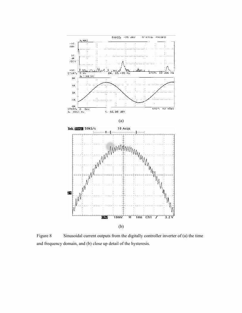
5.1 Inverter Operation
The DSP is programmed to generate a sinusoidal reference signal with a fundamental
frequency of 36Hz and a magnitude of 6A. The DSP also sets the current controller to
generate the output current with a hysteresis band of 0.1A. The upper plot of Figure 8(a)
shows the frequency spectrum of the current output. There is a large peak near 0Hz
representing the fundamental frequency. The asynchronous nature of the hysteresis current
controller is shown by the band of frequencies at 4.7kHz. The lower plot in Figure 8(a) shows
just over one cycle of the output current shown in the time domain. The current ripple is small
in comparison to the overall magnitude of the current and that there are no significant current
overshoots. Overshoots have occurred and Figure 8(b) shows one of these in one of the
positive half cycles of current. The circle 1.2ms to the left of centre shows where the current
has deviated from the reference by twice the design limit for the hysteresis controller. This
was due to the inverter controller sampling the injection current when it was just inside the
hysteresis limit. The hysteresis band in Figure 8(b) is relatively constant over the half cycle.
This indicates that the sampling frequency is high enough as there are no large current
overshoots.
A sample compensating current that would result from a three-phase bridge rectifier with
capacitive smoothing was generated artificially by the DSP. The fundamental frequency is
50Hz and the overall output current is 0.71ARMS, with a hysteresis band of 0.2A. The
waveform illustrated in Figure 9 is the time domain representation of the output current. The
didt of the output current has been increased by reducing the injection inductance so the current
can follow the higher frequency reference. This gives more switching operations at the top of
each current peak when the slope is near zero. This is seen in Figure 9 as increased current
noise at the top of the peaks. The experimental waveform in Figure 9 is very similar to that
generated by simulation and shown in Figure 5.
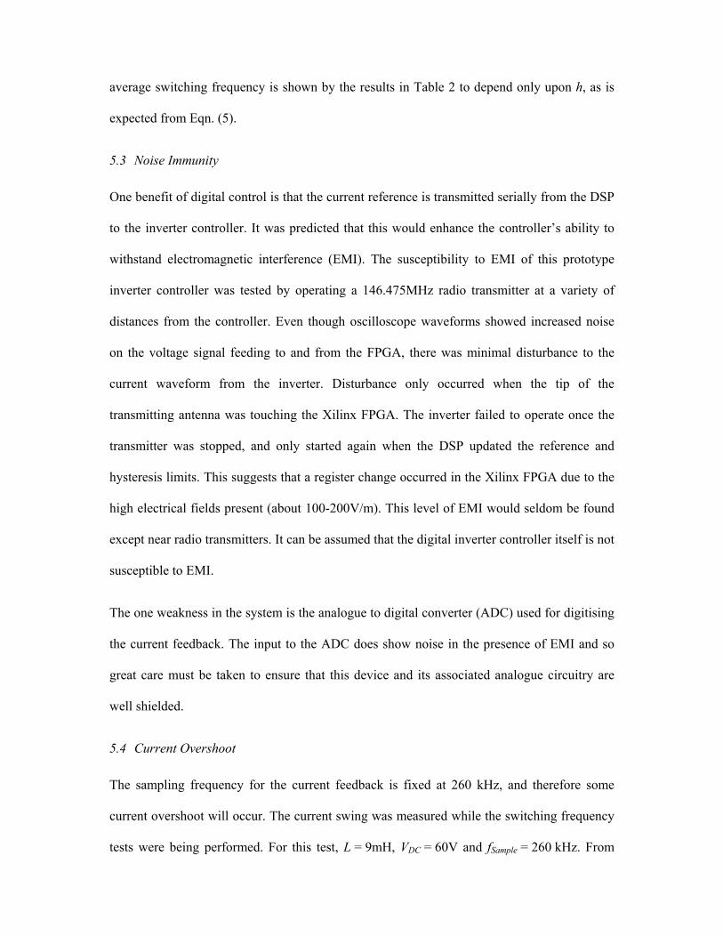
5.2 Average Switching Frequency
The hysteresis current controller ideally has a constant current ripple, ∆ i, but no defined
switching period ∆t (Brod and Novotny 1985). The maximum switching frequency occurs in a
hysteresis controlled inverter when the gradient of the reference current is near zero, as
illustrated in Figure 3. To test the validity of Equations (5) and (6) the inverter was operated
with a zero voltage reference to make the average inductor current zero. Table 1 summarises
the measurements taken. It can be seen that the calculated and observed results are very close
from where h = 0.2A.
Further tests were conducted with a single 60Hz sinusoid injected into the inductor. Table 2
shows the frequency and magnitude of the switching frequency with respect to the magnitude
of the 60Hz fundamental. The entries where the hysteresis limit is 10% of the peak current are
highlighted.
The results in Table 2 show that the magnitude of the switching noise is, on average, 4% of
the fundamental current when the hysteresis limit is one tenth of the reference current peak.
The lowest level of switching noise was with h = 0.1A, IP = 6.0A and was 0.5% of the
fundamental and is an improvement over the 3% magnitude obtained with h = 0.6A. The
average switching frequency is shown by the results in Table 2 to depend only upon h, as is
expected from Eqn. (5).
5.3 Noise Immunity
One benefit of digital control is that the current reference is transmitted serially from the DSP
to the inverter controller. It was predicted that this would enhance the controller’s ability to
withstand electromagnetic interference (EMI). The susceptibility to EMI of this prototype
inverter controller was tested by operating a 146.475MHz radio transmitter at a variety of
distances from the controller. Even though oscilloscope waveforms showed increased noise
on the voltage signal feeding to and from the FPGA, there was minimal disturbance to the
current waveform from the inverter. Disturbance only occurred when the tip of the
transmitting antenna was touching the Xilinx FPGA. The inverter failed to operate once the
transmitter was stopped, and only started again when the DSP updated the reference and
hysteresis limits. This suggests that a register change occurred in the Xilinx FPGA due to the
high electrical fields present (about 100-200V/m). This level of EMI would seldom be found
except near radio transmitters. It can be assumed that the digital inverter controller itself is not
susceptible to EMI.
The one weakness in the system is the analogue to digital converter (ADC) used for digitising
the current feedback. The input to the ADC does show noise in the presence of EMI and so
great care must be taken to ensure that this device and its associated analogue circuitry are
well shielded.
5.4 Current Overshoot
The sampling frequency for the current feedback is fixed at 260 kHz, and therefore some
current overshoot will occur. The current swing was measured while the switching frequency
tests were being performed. For this test, L = 9mH, VDC = 60V and fSample = 260 kHz. From
Eqn. (6) the value of overshoot, ∆ iOver, is 16mA. Table 3 summarises the level of overshoot
for six values of the hysteresis limit h.
Whilst the predicted maximum overshoot is independent of the hysteresis limit, h, this is not
so for the experimental results. Measuring small currents is difficult and the input to the
current feedback ADC has a noticeable level of noise. This will affect the inverter controller’s
ability to determine accurately when the current has exceeded the hysteresis band. It is
expected that by dealing with larger currents the effect of noise on the analogue circuitry will
be reduced.
6. Conclusion
A fully digital hysteresis current controller has been designed and implemented in a Xilinx
Field Programmable Gate Array. This completely digital controller makes the switching
decisions for hysteresis current control. The theoretical performance of a digital hysteresis
controller has been presented. The inverter controller has been tested on a small-scale
inverter, with experimental results providing performance data and verification of the
accuracy of the simulation model used.
The digital implementation of a hysteresis current controller was successful and performed as
expected. High levels of immunity to EMI make this type of current controller very promising
for use in full size high frequency switching inverters. A digital interface makes connection to
an active filter controller straightforward and robust. The controller is adaptable for use in any
application requiring current control of a voltage source inverter and is not limited to active
filtering.

Acknowledgments
Financial support for David Ingram was provided by the Metalect Industries (NZ) Ltd Power
Electronics Scholarship and by the Telecom Corporation of New Zealand Fellowship in
Telecommunications Engineering.

References
AKAGI, H., 1996. New Trends in Active Filters For Power Conditioning. IEEE Transactions on
Industry Applications, 32, 1312-1322.
BROD, D.M., NOVOTNY, D.W., 1985. Current Control of VSI-PWM Inverters. IEEE
Transactions on Industry Applications, IA-21, 562-570.
DUKE, R.M., ROUND, S.D., 1993. The Steady-State Performance of a Controlled Current
Active Filter. IEEE Transactions on Power Electronics, 8, 140-146.
LEE, H., SUH, B.S., HYUN, D.S., 1996. A Novel PWM Scheme for a Three-Level Voltage
Source Inverter with GTO Thyristors. IEEE Transactions on Industry Applications, 32, 260-268.
LI, Z., JIN, H., JOOS, G., 1995, Control of Active Filters Using Digital Signal Processors. 21st
International Conference on Industrial Electronics, Control and Instrumentation (IECON '95)
(Orlando, USA), 1, 651-655.
MALESANI, L., ROSSETTO, L., TOMASIN, P. ZUCCATO, A., 1996. Digital Adaptive
Hysteresis Current Control With Clocked Commutations and Wide Operating Range. IEEE
Transactions on Industry Applications, 32, 316-325.
RETIF, J.M., ALLARD, B., JORDA, X. PEREZ, A., 1993, Use of ASICs in PWM Techniques
for Power Converters. 19th International Conference on Industrial Electronics, Control and
Instrumentation (IECON '93) (Maui, Hawaii, USA), 2, 683-688.
SASAKI, H., MACHIDA, T., 1971. A New Method to Eliminate AC Harmonic Currents by
Magnetic Flux Compensation - Considerations on Basic Design. IEEE Transactions on Power
Apparatus and Systems, PAS-90, 2009-2019.
XILINX, 1996, The Programmable Logic Data Book (San Jose, California, USA: Xilinx).
Table 1 Maximum inverter switching frequency.
h (A) Max Frequency (kHz)
(½∆Ι) Calculated Observed
0.1 7.4 5.9
0.2 3.7 3.6
0.3 2.5 2.6
0.4 1.9 1.8
0.5 1.5 1.5
0.6 1.2 1.3
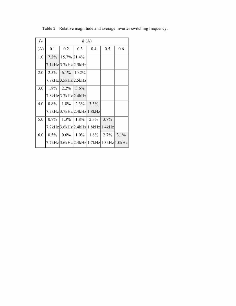
Table 2 Relative magnitude and average inverter switching frequency.
IP h (A)
(A) 0.1 0.2 0.3 0.4 0.5 0.6
1.0 7.2%
7.1kHz
15.7%
3.7kHz
21.4%
2.5kHz
2.0 2.5%
7.7kHz
6.1%
3.5kHz
10.2%
2.5kHz
3.0 1.8%
7.8kHz
2.2%
3.7kHz
3.6%
2.4kHz
4.0 0.8%
7.7kHz
1.8%
3.7kHz
2.3%
2.4kHz
3.3%
1.8kHz
5.0 0.7%
7.7kHz
1.3%
3.6kHz
1.8%
2.4kHz
2.3%
1.8kHz
3.7%
1.4kHz
6.0 0.5%
7.7kHz
0.6%
3.6kHz
1.0%
2.4kHz
1.8%
1.7kHz
2.7%
1.3kHz
3.1%
1.0kHz
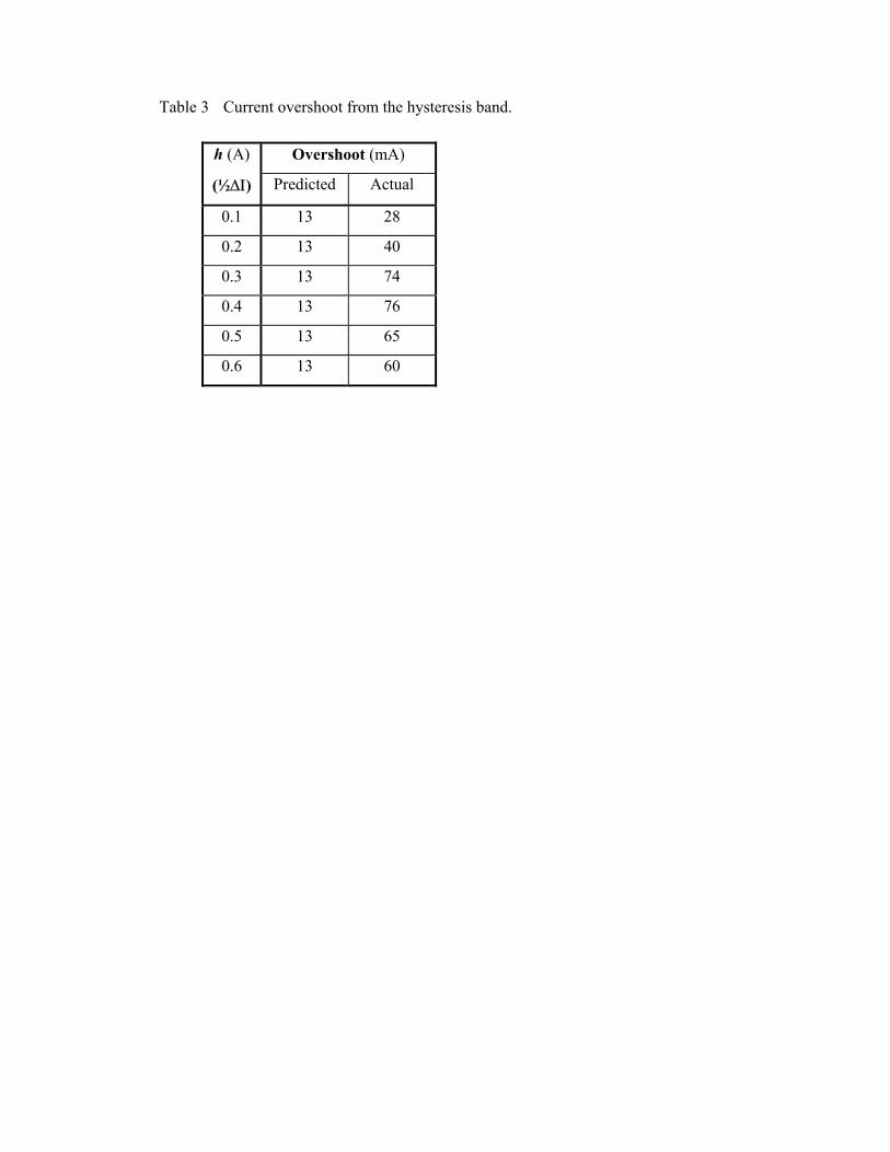
Table 3 Current overshoot from the hysteresis band.
h (A) Overshoot (mA)
(½∆Ι) Predicted Actual
0.1 13 28
0.2 13 40
0.3 13 74
0.4 13 76
0.5 13 65
0.6 13 60
FundamentalLoad Current
(a)
(b)
Figure 1 Load current for a three-phase bridge rectifier in (a) the time domain and (b)
the frequency domain.
Non-linearLoad
HarmonicIsolator
Three PhaseInverter
CurrentTransducer
DSP
Active Power Filter
PowerSystem
ILIC
I'C I'L
IS= +
Figure 2 Single line diagram of an active filter.
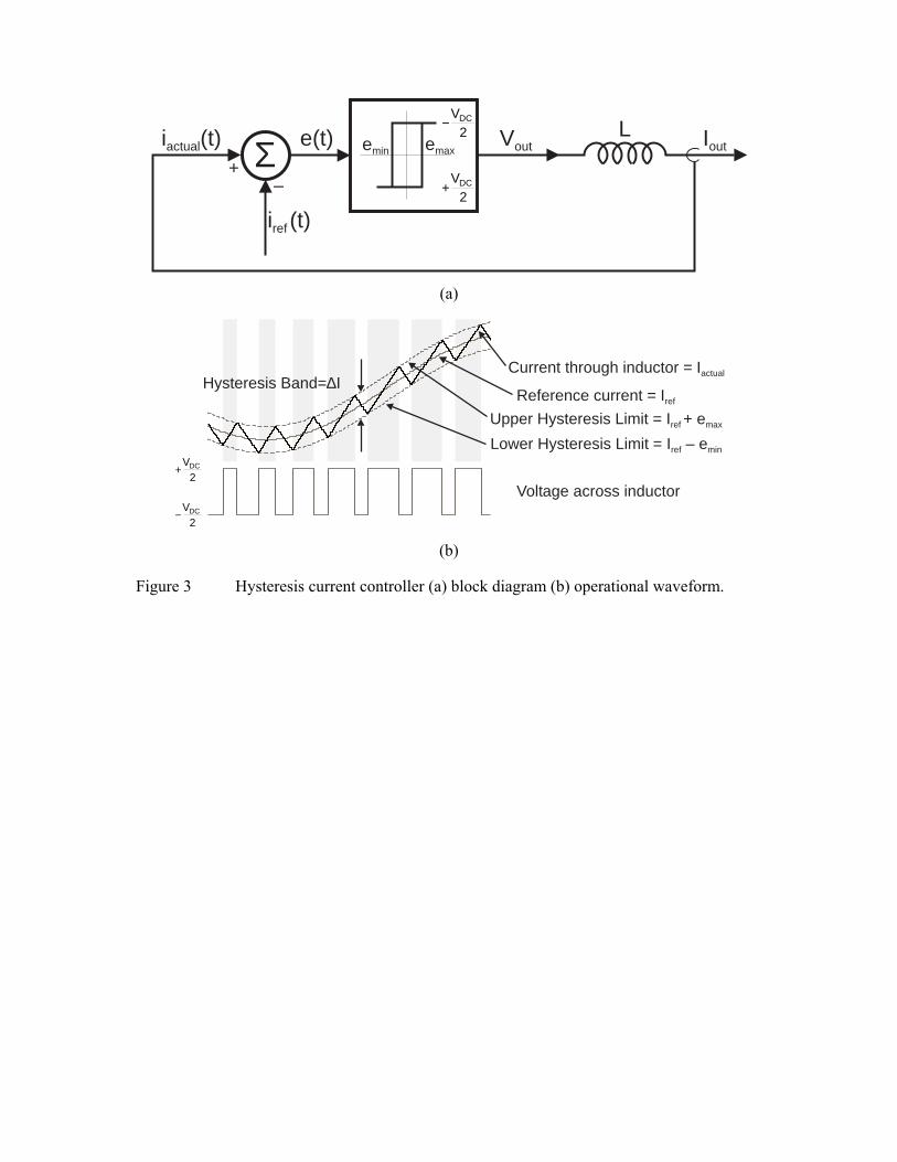
i tref ( )
i tactual( ) e t( ) LVout IoutΣ+–
−VDC
2
+VDC
2
emaxemin
(a)
Voltage across inductor
Current through inductor = Iactual
Reference current = Iref
Hysteresis Band=∆I
Lower Hysteresis Limit = I – eref min
Upper Hysteresis Limit = I + eref max
−VDC
2
+VDC
2
(b)
Figure 3 Hysteresis current controller (a) block diagram (b) operational waveform.
0 0.5 1 1.5 2 2.5 3 3.5 4−1
0
1
2
3
4
5
Time (ms)
Cur
rent
(A
)
5kHz Sampling
(a)
0 0.5 1 1.5 2 2.5 3 3.5 4−0.5
0
0.5
1
1.5
2
2.5
3
3.5
4
4.5
Time (ms)
Cur
rent
(A
)
260kHz Sampling
(b)
Figure 4 A higher sampling frequency reduces the level of current overshoot from the
hysteresis limits.
0 2 4 6 8 10 12 14 16 18 20−1.5
−1
−0.5
0
0.5
1
1.5
Time (ms)
Cur
rent
(A
)
Simulated Compensating Current
(a)
0 2 4 6 8 10 12 14 16 18 20−80
−70
−60
−50
−40
−30
−20
−10
0
Frequency (kHz)
Mag
nitu
de (
dBA
rms)
Simulated Compensating Current
(b)
Figure 5 Simulated compensating current output from Simulink.
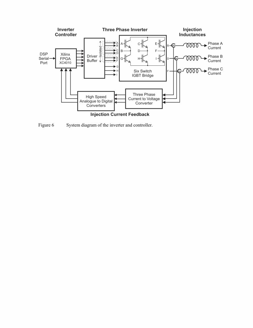
Figure 6 System diagram of the inverter and controller.
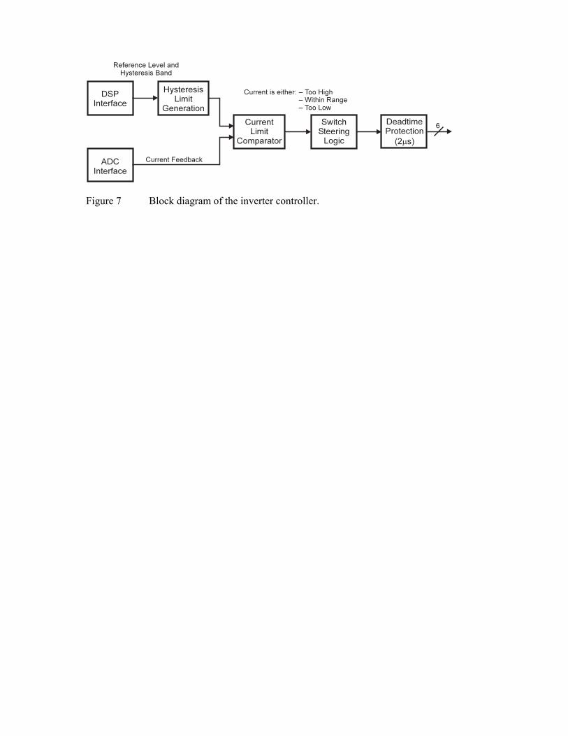
Figure 7 Block diagram of the inverter controller.
(a)
(b)
Figure 8 Sinusoidal current outputs from the digitally controller inverter of (a) the time
and frequency domain, and (b) close up detail of the hysteresis.
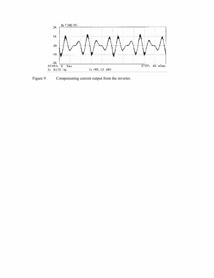
Figure 9 Compensating current output from the inverter.