A full band does not conduct. These concepts extended to 3D
88
Charge Carriers in Semiconductors 3s 3p GaAs A full band does not conduct. Electron in a band state moves at the group velocity. In 1D, = 1 ℏ Due to symmetry, the net velocity of all states of a band is zero. These concepts extended to 3D: g = 1 ℏ = 1 ℏ � + � + � The 1 st BZ is always symmetric, therefore net velocity of all states of a band is zero.
Transcript of A full band does not conduct. These concepts extended to 3D

Charge Carriers in Semiconductors
3s
3p
GaAs
A full band does not conduct.
Electron in a band state moves at the group velocity.
In 1D, 𝑣𝑣𝑔𝑔 =1ℏ𝑑𝑑𝑑𝑑𝑑𝑑𝑑𝑑
Due to symmetry, the net velocity of all states of a band is zero.
These concepts extended to 3D:
𝐯𝐯g =1ℏ𝛻𝛻𝐤𝐤𝑑𝑑 =
1ℏ
�𝐱𝐱𝜕𝜕𝑑𝑑𝜕𝜕𝑑𝑑𝑥𝑥
+ �𝐲𝐲𝜕𝜕𝑑𝑑𝜕𝜕𝑑𝑑𝑦𝑦
+ �𝐳𝐳𝜕𝜕𝑑𝑑𝜕𝜕𝑑𝑑𝑧𝑧
The 1st BZ is always symmetric, therefore net velocity of all states of a band is zero.

Counting electrons
3s
3p
GaAs
3s
3p
Si
Examples: Si (group IV element, diamond structure) & GaAs (octet compound, zincblende structure)
For a crystal of N primitive unit cells,there are N band states each band, i.e., N distinct k in the 1st BZ.
The N states in each band accommodate 2N electrons.
There are 4 bands originating from valence electron orbitals, together accommodating 4N × 2 = 8N electrons.
For diamond & zincblende structures, each primitive unit cell contains 2 atoms. Each primitive unit cell contributes 4 × 2 = 8 valence electrons.
N primitive unit cells have 8N valence electrons.
Therefore the bands of valence electrons are full.

Motion of single electron near a band minimum
Si:
GaAs:
Near a band minimum, the E-k dispersion can be written as (Taylor expansion):
𝑑𝑑 𝑑𝑑 = 𝑑𝑑 𝑑𝑑0 +12
�𝜕𝜕2𝑑𝑑𝜕𝜕𝑑𝑑2
𝑘𝑘=𝑘𝑘0
(𝑑𝑑 − 𝑑𝑑0)2
(good approx. near a minimum)
If we consider 𝑑𝑑 𝑑𝑑0 as a potential energy V, and ℏ(𝑑𝑑 − 𝑑𝑑0) as a momentum p, then this becomes formally the same as a classical particle:
The “effective mass” of the electron, 𝑚𝑚𝑒𝑒∗ ,
can be found by:1𝑚𝑚𝑒𝑒∗ =
1ℏ2
�𝜕𝜕2𝑑𝑑𝜕𝜕𝑑𝑑2
𝑘𝑘=𝑘𝑘0
We use a 1D heuristic for simple math. In 3D, the second derivative is a tensor (the effective mass is anisotropic), and 𝑑𝑑0 ← 𝐤𝐤0 may or may not be zero.
𝐤𝐤0 ≠ 0
𝐤𝐤0 = 0⇔

In this semiclassical model, ℏ𝑑𝑑𝑑𝑑𝑑𝑑𝑑𝑑
= ℏ𝑑𝑑𝑑𝑑𝑑𝑑
(𝑑𝑑 − 𝑑𝑑0) = 𝐹𝐹
𝑣𝑣𝑔𝑔 =1ℏ𝑑𝑑𝑑𝑑𝑑𝑑𝑑𝑑
=1ℏ
𝑑𝑑𝑑𝑑𝑑𝑑(𝑑𝑑 − 𝑑𝑑0)
Force on electron
The electron is pushed by the force to move in k-space. At each k, the electron’s velocity is the group velocity:
The effective mass of the electron, 𝑚𝑚𝑒𝑒∗ , is defined for the band minimum at 𝐤𝐤0:
1𝑚𝑚𝑒𝑒∗ =
1ℏ2
�𝜕𝜕2𝑑𝑑𝜕𝜕𝑑𝑑2
𝑘𝑘=𝑘𝑘0
⇔
Near the band minimum, the E-k dispersion is well approximated by:
𝑝𝑝 = 𝑚𝑚𝑒𝑒∗𝑣𝑣𝑔𝑔 = ℏ(𝑑𝑑 − 𝑑𝑑0)
𝐩𝐩 = ℏ(𝐤𝐤 − 𝐤𝐤0) in 3D
Question: Describe the motion of a single electron added to a perfect, static (T = 0) semiconductor crystal in a constant electric field.
Notice that 𝐯𝐯g = 0 at a minimum 𝐤𝐤 = 𝐤𝐤0.
𝐯𝐯g =1ℏ𝛻𝛻𝐤𝐤𝑑𝑑 =
1ℏ
�𝐱𝐱𝜕𝜕𝑑𝑑𝜕𝜕𝑑𝑑𝑥𝑥
+ �𝐲𝐲𝜕𝜕𝑑𝑑𝜕𝜕𝑑𝑑𝑦𝑦
+ �𝐳𝐳𝜕𝜕𝑑𝑑𝜕𝜕𝑑𝑑𝑧𝑧

We have learned:
A full band does not conduct.
The valence bands are full and conduction bands empty for perfect, pure semiconductors at T = 0. No conduction.
To conduct, need charge carriers, e.g., electrons near the conduction band minimum.
The semiclassical model works well in most circumstances, because mobile electrons are near the conduction band minimum/bottom (CBM):
• in equilibrium, these mobile electrons only occupy states near CBM with non-vanishing probabilities;
• when driven by a field, these electron can not go far from equilibrium, since each is “thermalized” by collision every time interval 𝜏𝜏.
We will later discuss how these carriers distribute in the conduction band states.

The concept of the hole
(A full band of electrons do not conduct.)
0)( =∑k
kvConsider the topmost filled band (valence band),
Here v is short for 𝐯𝐯g, the velocity of each electron
Somehow one electron at 𝐤𝐤𝑒𝑒 is removed.
𝐤𝐤𝑒𝑒
⇒
The motion of all the electrons in this band can be described as the motion of this vacancy.
1𝑚𝑚𝑒𝑒∗ =
1ℏ2
�𝜕𝜕2𝑑𝑑𝜕𝜕𝑑𝑑2
𝑘𝑘=𝑘𝑘0
The effective mass of the empty state is
Wavevector of VBM
𝐯𝐯𝑒𝑒 𝐤𝐤𝑒𝑒 + �𝐤𝐤≠𝐤𝐤𝑒𝑒
𝐯𝐯(𝐤𝐤) = 0
𝐯𝐯𝑒𝑒 𝐤𝐤𝑒𝑒 = − �𝐤𝐤≠𝐤𝐤𝑒𝑒
𝐯𝐯(𝐤𝐤)

Grundmann, The Physicsof Semiconductors, p. 183.
1𝑚𝑚𝑒𝑒∗ =
1ℏ2
�𝜕𝜕2𝑑𝑑𝜕𝜕𝑑𝑑2
𝑘𝑘=𝑘𝑘0
The effective mass of the empty state is
Wavevector of VBM, not the empty state
We define the hole energy 𝑑𝑑ℎ = −𝑑𝑑, then the hole effective mass is
1𝑚𝑚ℎ∗ = −
1𝑚𝑚𝑒𝑒∗ = −
1ℏ2
�𝜕𝜕2𝑑𝑑𝜕𝜕𝑑𝑑2
𝑘𝑘=𝑘𝑘0
=1ℏ2
�𝜕𝜕2𝑑𝑑ℎ𝜕𝜕𝑑𝑑2
𝑘𝑘=𝑘𝑘0
So, it is positive.
In equilibrium, the hole is most likely to be at 𝑑𝑑 = 𝑑𝑑0.
A positive electric field ℰ will drive the entire band of electrons towards the negative, thus the empty state moves to 𝑑𝑑𝑒𝑒 = 𝑑𝑑0 + ∆𝑑𝑑, where ∆𝑑𝑑 = −𝑞𝑞ℰ𝜏𝜏/ℏ.The corresponding momentum ℏ(𝑑𝑑𝑒𝑒 − 𝑑𝑑0) and group velocity 𝑣𝑣𝑒𝑒 are negative.
Convenient to define the hole charge to be +q, thus moved towards the positive by the positive ℰ. Therefore, 𝑑𝑑ℎ = 𝑑𝑑0 − ∆𝑑𝑑, so that momentum ℏ(𝑑𝑑ℎ − 𝑑𝑑0) and group velocity 𝑣𝑣ℎ are positive.
The hole carries charge +q, and has a positive effective mass near VBM.

Carriers in semiconductorsFermi-Dirac distribution of electrons: consequence of Pauli’s exclusion rule
Fermi-Dirac distribution at T = 0:f(E) is the probability of a state at energy E being occupied.
Analogy: sand particles in a vessel
semiconductor
EF
EC
EV
In this kind of chart, lines just signifies energy levels, horizontal coordinate means nothing.
For semiconductors, with a gap, EF is somewhat arbitrary.
EF depends on total amount of sand particles and available volume of the vessel per height (non-cylindrical vessel), ortotal number of electrons and number of available states per energy interval (per volume)
(Recall our calculation of in the Drude-Sommerfeld model)

The Fermi level EF(T) is a function of T.Fermi level vs. chemical potential: difference in terminology in different fields.(See next slide)
Since EF depends on number of available states per energy interval (per volume), the way EF(T) varies with T depends on it.
What is this called?
Fermi-Dirac distribution at T = 0: Imagine each sand particle is energetic

Digression:Subtle difference in jargons used by EEs and physicists
We use the EE terminology, of course.
EF = EF(T)
Physicists:
Chemical potential µ(T)
Fermi level
Fermi energy EF = µ(0)
Same concept when T > 0
We already used µ for mobility.

From Shockley, Electrons and Holes in Semiconductors, 1976 (original ed.1950)
Density of states (DOS) determines how EF(T) varies with T.In this illustration, you may consider the electrons spinless or each small box a spin-Bloch state.
(a) 20 electrons at T = 0. (b) T > 0, some electrons promoted to higher energies. If EF remained ~ the same, we would need 21 electrons. (c) To keep the # of electrons unchanged, EF has to move down. The lower band is still full at low T.(d) At higher T, EF moves further down and the distribution flattens more, so that some states in lower band vacate.

How to find density of states D(E)
1D case:Each k occupies 2π/L in k-space.
The take-home message is
Here, 𝐷𝐷 𝑑𝑑 ∝ 𝐿𝐿 is the number of states per energy interval in the entire length L of the 1D semiconductor.
In the interval dk, there are
states.
Translate this 𝐷𝐷 𝑑𝑑 𝑑𝑑𝑑𝑑 to 𝐷𝐷 𝑑𝑑 𝑑𝑑𝑑𝑑near a band extremum at 𝑑𝑑0:
𝑑𝑑 𝑑𝑑 = 𝑑𝑑 𝑑𝑑0 +ℏ2(𝑑𝑑 − 𝑑𝑑0)2
2𝑚𝑚∗
𝑑𝑑𝑑𝑑 =ℏ2
2𝑚𝑚∗ 2 𝑑𝑑 − 𝑑𝑑0 𝑑𝑑𝑑𝑑⇒
=ℏ2
𝑚𝑚∗ 𝑑𝑑 − 𝑑𝑑0 𝑑𝑑𝑑𝑑
And, 𝑑𝑑 − 𝑑𝑑0 = 2𝑚𝑚∗[𝑑𝑑 − 𝑑𝑑 𝑑𝑑0 ]/ℏ
𝐷𝐷 𝑑𝑑 𝑑𝑑𝑑𝑑 =𝐿𝐿
2𝜋𝜋𝑚𝑚∗
ℏ2 𝑑𝑑 − 𝑑𝑑0𝑑𝑑𝑑𝑑
=𝐿𝐿
2𝜋𝜋ℏ𝑚𝑚∗
2[𝑑𝑑 − 𝑑𝑑 𝑑𝑑0 ]𝑑𝑑𝑑𝑑
𝐷𝐷 𝑑𝑑 ∝ [𝑑𝑑 − 𝑑𝑑 𝑑𝑑0 ]−1/2
𝑑𝑑 𝑑𝑑0

3D case:Recall from Slide 9 of Lecture Note 4:
𝑑𝑑𝑥𝑥 =2𝜋𝜋𝐿𝐿𝑛𝑛𝑥𝑥 𝑑𝑑𝑦𝑦 =
2𝜋𝜋𝐿𝐿𝑛𝑛𝑦𝑦 𝑑𝑑𝑧𝑧 =
2𝜋𝜋𝐿𝐿𝑛𝑛𝑧𝑧
Each state |k⟩ occupies a volume (2𝜋𝜋)3/𝑉𝑉 in the wavevector space.
𝑑𝑑 𝐤𝐤 = 𝑑𝑑 𝐤𝐤0 +ℏ2(𝐤𝐤 − 𝐤𝐤0)2
2𝑚𝑚∗We consider a simple case where 𝑑𝑑 𝐤𝐤 is isotropic:
The volume of a spherical shell with a thickness dq and radius qin k-space is 4𝜋𝜋𝑞𝑞2𝑑𝑑𝑞𝑞.
𝐤𝐤0
dqq
Here we just use q to represent |𝐤𝐤 − 𝐤𝐤0| for the moment. We will continue to use it for the electron charge later.
𝐷𝐷 𝑞𝑞 𝑑𝑑𝑞𝑞 =4𝜋𝜋𝑞𝑞2𝑑𝑑𝑞𝑞(2𝜋𝜋)3/𝑉𝑉
=𝑉𝑉
2𝜋𝜋2𝑞𝑞2𝑑𝑑𝑞𝑞
𝑑𝑑 𝐤𝐤 = 𝑑𝑑 𝐤𝐤0 +ℏ2𝑞𝑞2
2𝑚𝑚∗ 𝑑𝑑𝑑𝑑 =ℏ2
𝑚𝑚∗ 𝑞𝑞𝑑𝑑𝑞𝑞⇒⇒ 𝐷𝐷 𝑑𝑑 𝑑𝑑𝑑𝑑 =
𝑉𝑉2𝜋𝜋2
𝑚𝑚∗
ℏ2𝑞𝑞𝑑𝑑𝑑𝑑
⇓
𝑞𝑞 = 2𝑚𝑚∗[𝑑𝑑 − 𝑑𝑑 𝐤𝐤0 ]/ℏ ⇒
⇓
𝐷𝐷 𝑑𝑑 𝑑𝑑𝑑𝑑 =𝑉𝑉
2𝜋𝜋22(𝑚𝑚∗)3/2
ℏ3𝑑𝑑 − 𝑑𝑑 𝐤𝐤0 𝑑𝑑𝑑𝑑

The take-home message is𝐷𝐷 𝑑𝑑 ∝ [𝑑𝑑 − 𝑑𝑑 𝐤𝐤0 ]1/2
𝑑𝑑 𝐤𝐤0
For the conduction band, 𝐷𝐷 𝑑𝑑 ∝ (𝑑𝑑 − 𝑑𝑑𝐶𝐶)1/2
For the valence band, 𝐷𝐷 𝑑𝑑 ∝ (𝑑𝑑𝑉𝑉 − 𝑑𝑑)1/2
𝐷𝐷 𝑑𝑑 𝑑𝑑𝑑𝑑 =𝑉𝑉
2𝜋𝜋22(𝑚𝑚∗)3/2
ℏ3𝑑𝑑 − 𝑑𝑑 𝐤𝐤0 𝑑𝑑𝑑𝑑
Here, we take 𝑚𝑚∗ as one parameter. Real world semiconductors are more complicated.
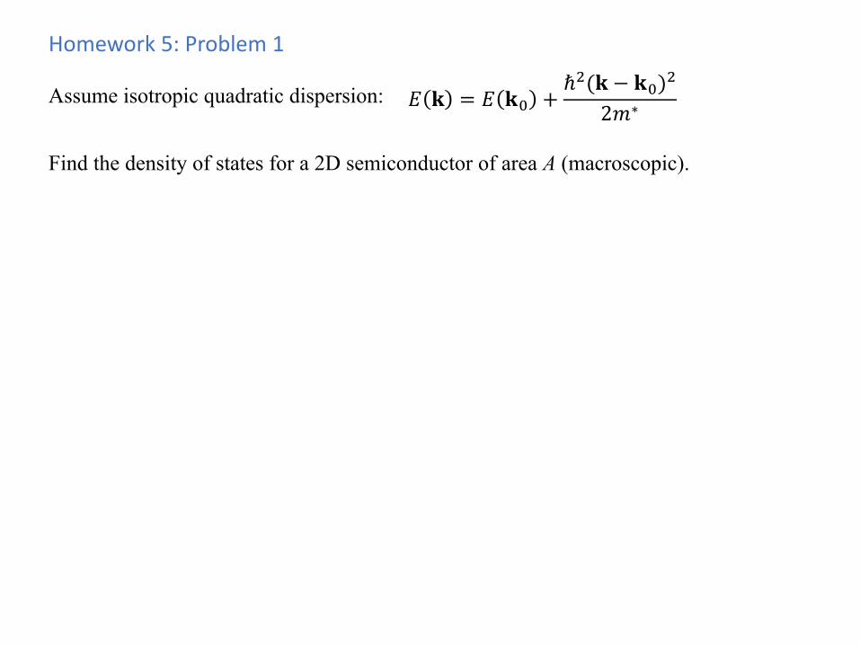
Homework 5: Problem 1
𝑑𝑑 𝐤𝐤 = 𝑑𝑑 𝐤𝐤0 +ℏ2(𝐤𝐤 − 𝐤𝐤0)2
2𝑚𝑚∗Assume isotropic quadratic dispersion:
Find the density of states for a 2D semiconductor of area A (macroscopic).
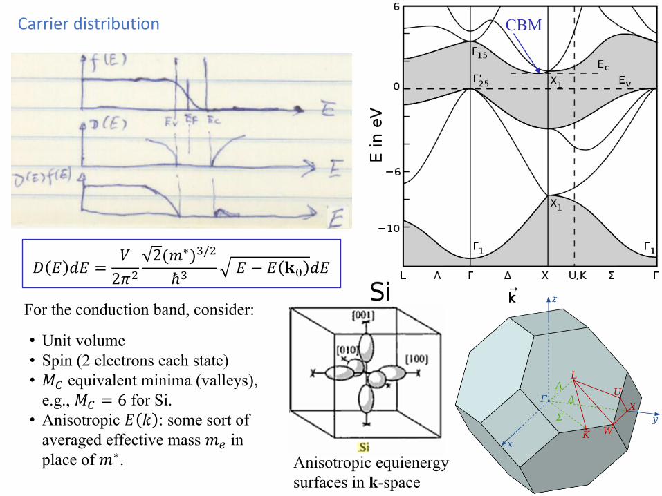
Carrier distribution
𝐷𝐷 𝑑𝑑 𝑑𝑑𝑑𝑑 =𝑉𝑉
2𝜋𝜋22(𝑚𝑚∗)3/2
ℏ3𝑑𝑑 − 𝑑𝑑 𝐤𝐤0 𝑑𝑑𝑑𝑑
Anisotropic equienergysurfaces in k-space
For the conduction band, consider:
• Unit volume• Spin (2 electrons each state)• 𝑀𝑀𝐶𝐶 equivalent minima (valleys),
e.g., 𝑀𝑀𝐶𝐶 = 6 for Si.• Anisotropic 𝑑𝑑 𝑑𝑑 : some sort of
averaged effective mass 𝑚𝑚𝑒𝑒 in place of 𝑚𝑚∗.
CBM

𝐷𝐷 𝑑𝑑 𝑑𝑑𝑑𝑑 =𝑉𝑉
2𝜋𝜋22(𝑚𝑚∗)3/2
ℏ3𝑑𝑑 − 𝑑𝑑 𝐤𝐤0 𝑑𝑑𝑑𝑑
For the conduction band, consider:
• Unit volume• Spin (2 electrons each state)• 𝑀𝑀𝐶𝐶 equivalent minima (valleys),
e.g., 𝑀𝑀𝐶𝐶 = 6 for Si.• Anisotropic 𝑑𝑑 𝑑𝑑 : some sort of
averaged effective mass 𝑚𝑚𝑒𝑒 in place of 𝑚𝑚∗.
𝑛𝑛 = �𝐸𝐸𝐶𝐶
∞𝑀𝑀𝐶𝐶
1𝜋𝜋2
2 𝑚𝑚𝑒𝑒3/2
ℏ3𝑑𝑑 − 𝑑𝑑𝐶𝐶 𝑓𝑓(𝑑𝑑)𝑑𝑑𝑑𝑑
This integral (called a Fermi integral) cannot be solved analytically.When 𝑑𝑑 − 𝑑𝑑𝐹𝐹 > 4𝑑𝑑𝐵𝐵𝑇𝑇 ~ 0.1 eV, 𝑒𝑒4 ≈ 55 >> 1 thus 𝑓𝑓(𝑑𝑑) reduces to Boltzmann distribution.
Grundmann, The Physics of Semiconductors, p. 862
k for 𝑑𝑑𝐵𝐵

Digression: Physical justification of Boltzmann approximation to F-D distribution
F-D distribution is the consequence of Pauli’s exclusion rule. Since there are very few electrons at 𝑑𝑑 − 𝑑𝑑𝐹𝐹 > 4𝑑𝑑𝐵𝐵𝑇𝑇, Pauli’s exclusion rule does not matter – electrons won’t run into each other anyway, just like molecules in an ideal gas.
With this approximation, the integral can be taken analytically, yielding
𝑛𝑛 = �𝐸𝐸𝐶𝐶
∞𝑀𝑀𝐶𝐶
1𝜋𝜋2
2 𝑚𝑚𝑒𝑒3/2
ℏ3𝑑𝑑 − 𝑑𝑑𝐶𝐶 𝑓𝑓(𝑑𝑑)𝑑𝑑𝑑𝑑
𝑀𝑀𝐶𝐶
Notice the T dependence here!
as if all conduction band electrons are at 𝑑𝑑𝐶𝐶 , where there are 𝑁𝑁𝐶𝐶 states per unit volume.
Grundmann, The Physics of Semiconductors, p. 184
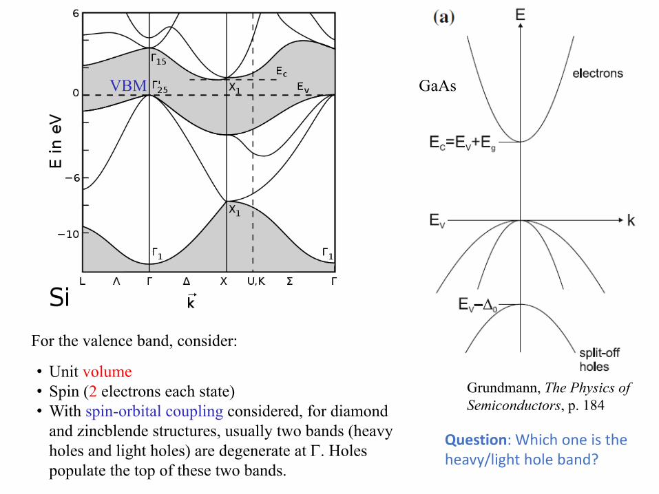
VBM
For the valence band, consider:
• Unit volume• Spin (2 electrons each state)• With spin-orbital coupling considered, for diamond
and zincblende structures, usually two bands (heavy holes and light holes) are degenerate at Γ. Holes populate the top of these two bands.
Question: Which one is the heavy/light hole band?
GaAs

Grundmann, The Physics of Semiconductors, p. 184
GaAs
𝐷𝐷 𝑑𝑑 𝑑𝑑𝑑𝑑 =𝑉𝑉
2𝜋𝜋22(𝑚𝑚∗)3/2
ℏ3𝑑𝑑 − 𝑑𝑑 𝐤𝐤0 𝑑𝑑𝑑𝑑
For the valence band, consider:• Unit volume• Spin (2 electrons each state)• With spin-orbital coupling considered, for diamond
and zincblende structures, usually two bands (heavy holes and light holes) are degenerate at Γ. Holes populate the top of these two bands.
Some sort of “total” effective mass 𝑚𝑚ℎ considering both light and heavy holes in place of 𝑚𝑚∗.
𝑝𝑝 = �−∞
𝐸𝐸𝑉𝑉 1𝜋𝜋2
2 𝑚𝑚ℎ3/2
ℏ3𝑑𝑑𝑉𝑉 − 𝑑𝑑 [1 − 𝑓𝑓 𝑑𝑑 ]𝑑𝑑𝑑𝑑
Again, Boltzmann approximation yields analytical form:

Grundmann, The Physics of Semiconductors, p. 207
How good the approximation is

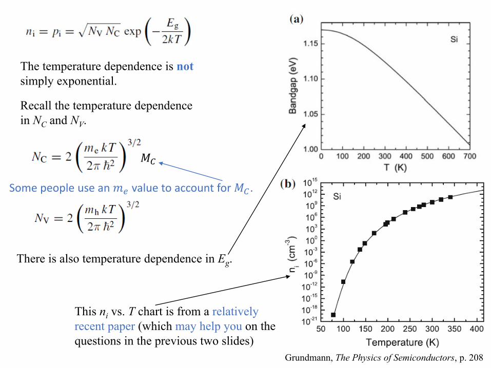
Intrinsic carriers
Charge neutrality:
For Si (Eg = 1.12eV) at T = 300 K, kT = 25.9 meV, Eg/kT = 43.2, 𝑒𝑒21.6 = 2.45 × 10⁹.Many text books listNC = 2.8 × 10¹⁹/cm3, NV = 1.04 × 10¹⁹/cm3, and ni = 1.45 × 10¹⁰/cm3, as if this ni value was calculated with the above equation. Do your own calculation and see what you get.
Then, check out this document on the web: https://ecee.colorado.edu/~bart/book/ex019.htmLook for NC, NV, and ni at 300 K. Find out how consistent the ni is with NC and NV.
Grundmann, The Physics of Semiconductors, p. 209

The list in a relatively new book Grundmann, The Physics of Semiconductors (2016):
Examine how consistent the ni value is with the NC and NV values here.
Read the online discussions here: https://www.researchgate.net/post/Proper_calculation_of_intrinsic_carrier_concentration_in_silicon_at_300_K_with_erroneous_illustration_in_certain_frequently_followed_textbooks
What do you think? What’s the impact of any inaccuracy?Do a literature search and try to find out why there has been this issue. If you use or have access to simulators, try to find out what values are used.

For the intrinsic semiconductor,
Insert the various NC and NV values you found. Think about the difference in results in the context of the questions in the last slide.
This is the intrinsic Fermi level.
𝑀𝑀𝐶𝐶
The temperature dependence is notsimply exponential.
Recall the temperature dependence in NC and NV.
Some people use an 𝑚𝑚𝑒𝑒 value to account for 𝑀𝑀𝐶𝐶 .
There is also temperature dependence in Eg.
Grundmann, The Physics of Semiconductors, p. 208
This ni vs. T chart is from a relatively recent paper (which may help you on the questions in the previous two slides)

DopingCarriers can be introduced by shallow defects.Shallow donors: group V dopants in group IV semiconductor, e.g., P in Si.
The P substitution of a Si atom perturbs the Si lattice. The extra e wanders in the long-range Coulomb potential of the P+ ion. This long-range potential determines the energy levels of the bound e. The H atom model approximates this situation.
Binding energy of shallow donor: electron chargeelectron effective mass in semiconductor
Free electron mass
dielectric constant of semiconductor
Bohr radius of H atom, 0.053 nm
binding energy of 1s electron in H atom (13.6 eV)
Bohr radius of shallow donor:
Vacuum, E = 0
𝑑𝑑1 = −13.6 eV
13.6 eV
H atom
𝑑𝑑𝐷𝐷
Shallow donor
𝑑𝑑𝐶𝐶𝑑𝑑𝐷𝐷𝑏𝑏
For Si, 𝑚𝑚𝑒𝑒∗/𝑚𝑚0 ~ 0.3, 𝜀𝜀𝑟𝑟 = 11.9.
𝑑𝑑𝐷𝐷𝑏𝑏 ~ 29 meV𝑎𝑎𝐷𝐷 ~ 2.1 nm. Compare this to Si lattice parameter – shallow donor!

In contrast, deep defect potentials are short ranged, ⇒ the bound electron wave functions are highly localized.
⇒ The deep defects trap carriers(The energy levels are often “deep” (close to midgap), but not always)
Impurity levels in Si
(Li is interstitial) Grundmann, The Physics of Semiconductors, p. 212
Binding energies of P, As, Sb agree reasonably well with the H model (29 meV).

𝑑𝑑𝐷𝐷
Shallow donor
𝑑𝑑𝐶𝐶𝑑𝑑𝐷𝐷𝑏𝑏
For Si, 𝑚𝑚𝑒𝑒∗/𝑚𝑚0 ~ 0.3, 𝜀𝜀𝑟𝑟 = 11.9.
𝑑𝑑𝐷𝐷𝑏𝑏 ~ 29 meV𝑎𝑎𝐷𝐷 ~ 2.1 nm. Compare this to Si lattice parameter – shallow donor!
The bound electron is not a mobile carrier. It is attracted to the P+.
The Bohr model approximates P0.
The P+ with a bound e makes P0 – the neutral or un-ionized donor. (not union-ized)
The bound e may gain enough energy (≥ 𝑑𝑑𝐷𝐷𝑏𝑏) to escape, and become a mobile e in CB. The P+ left behind is an ionized (charged) donor.

Shallow acceptors: group III dopants in group IV semiconductor, e.g., B in Si.Consider the valence band full, i.e., each of 4 bonds of B made of a valence electron pair. (Full band does not conduct.)
The valence band is filled with a borrowed valence electron. “Borrowed” from the entire system, which has a deficit of 1 valence electron. This deficit is accounted for by the bound hole.
The bound hole is not a mobile carrier. It is attracted to the B−.
The Bohr model provides a simple approximation, although not so well as for shallow donors, due to degeneracy of VBM (light, heavy holes).
The B− with a bound hole makes B0 – the neutral or un-ionized acceptor. (not union-ized)
𝑑𝑑𝑉𝑉Shallow acceptor
𝑑𝑑𝐴𝐴𝑑𝑑𝐴𝐴𝑏𝑏
The bound hole may gain enough energy (≥ 𝑑𝑑𝐴𝐴𝑏𝑏) to escape, and become a mobile hole in VB. The B− left behind is an ionized (charged) acceptor.

n-type doping by shallow donors
𝑁𝑁𝐷𝐷 : donor concentration𝑁𝑁𝐷𝐷+: ionized donor concentration𝑁𝑁𝐷𝐷0: neutral donor concentration
Grundmann, The Physics of Semiconductors, p. 209
It is tempting to think that
𝑁𝑁𝐷𝐷+
𝑁𝑁𝐷𝐷0= 𝑒𝑒−
𝐸𝐸𝐷𝐷𝑏𝑏
𝑘𝑘𝑘𝑘
At RT, 𝐸𝐸𝐷𝐷𝑏𝑏
𝑘𝑘𝑘𝑘~ 1.5 to 2 ⇒
𝑁𝑁𝐷𝐷+𝑁𝑁𝐷𝐷0
~ 0.2
But, we have always assumed that essentially all donors are ionized, 𝑛𝑛 = 𝑁𝑁𝐷𝐷+ = 𝑁𝑁𝐷𝐷
Why?

The F-D distribution
𝑁𝑁𝐷𝐷0
𝑁𝑁𝐷𝐷+= 𝑒𝑒−
𝐸𝐸𝐷𝐷−𝐸𝐸𝐹𝐹𝑘𝑘𝑘𝑘 = 𝑒𝑒
𝐸𝐸𝐹𝐹−𝐸𝐸𝐷𝐷𝑘𝑘𝑘𝑘
𝑓𝑓 𝑑𝑑 =1
𝑒𝑒𝐸𝐸−𝐸𝐸𝐹𝐹𝑘𝑘𝑘𝑘 + 1
The probability a donor state is neutral (D0):
𝑓𝑓 𝑑𝑑𝐷𝐷 =1
𝑒𝑒𝐸𝐸𝐷𝐷−𝐸𝐸𝐹𝐹𝑘𝑘𝑘𝑘 + 1
The probability a donor state is ionized (D+):
1 − 𝑓𝑓 𝑑𝑑𝐷𝐷 =𝑒𝑒𝐸𝐸𝐷𝐷−𝐸𝐸𝐹𝐹𝑘𝑘𝑘𝑘
𝑒𝑒𝐸𝐸𝐷𝐷−𝐸𝐸𝐹𝐹𝑘𝑘𝑘𝑘 + 1
Therefore,
(This is incorrect, but does not affect the big picture. Will correct soon)
Now we may say, 𝐸𝐸𝐹𝐹−𝐸𝐸𝐷𝐷𝑘𝑘𝑘𝑘
<< −1, therefore 𝑁𝑁𝐷𝐷0𝑁𝑁𝐷𝐷+
~ 0. But, saying so is self-fulfilling
(and 𝐸𝐸𝐹𝐹−𝐸𝐸𝐷𝐷𝑘𝑘𝑘𝑘
>> −1 is not necessarily true).

Charge neutrality:𝑛𝑛 = 𝑁𝑁𝐷𝐷+ + 𝑝𝑝
⇒
𝑁𝑁𝐷𝐷+ =𝑁𝑁𝐷𝐷
1 + 𝑒𝑒𝐸𝐸𝐹𝐹−𝐸𝐸𝐷𝐷𝑘𝑘𝑘𝑘
𝑁𝑁𝐷𝐷0
𝑁𝑁𝐷𝐷+= 𝑒𝑒−
𝐸𝐸𝐷𝐷−𝐸𝐸𝐹𝐹𝑘𝑘𝑘𝑘 = 𝑒𝑒
𝐸𝐸𝐹𝐹−𝐸𝐸𝐷𝐷𝑘𝑘𝑘𝑘
𝑁𝑁𝐶𝐶 ≫ 𝑁𝑁𝐷𝐷 ⇒Nearly all donors must ionize to satisfy
This holds up to 𝑁𝑁𝐷𝐷~1018 cm−3.
𝑁𝑁𝐶𝐶 is the effective DOS of CB. There are a lot more CB states near 𝑑𝑑𝐶𝐶than donor states at 𝑑𝑑𝐷𝐷.
(to be corrected)
S. M. Sze (施敏), Physics of Semiconductor Devices.

𝑑𝑑𝐷𝐷
𝑑𝑑𝐶𝐶𝑑𝑑𝐷𝐷𝑏𝑏
𝑁𝑁𝐷𝐷0
𝑁𝑁𝐷𝐷+= 𝑒𝑒−
𝐸𝐸𝐷𝐷−𝐸𝐸𝐹𝐹𝑘𝑘𝑘𝑘 = 𝑒𝑒
𝐸𝐸𝐹𝐹−𝐸𝐸𝐷𝐷𝑘𝑘𝑘𝑘 (This is incorrect, but does not affect
the big picture. We correct it now)
We did not consider the following:• Each donor level is 2-fold degenerate when neutral, i.e.,
neutral donor DOS is 2𝑁𝑁𝐷𝐷.• But, each donor atom can only have 1 bound electron.
(There cannot be D−.) • Each donor level is nondegenerate when ionized, i.e.,
ionized donor DOS is 𝑁𝑁𝐷𝐷+.
Consider the above and do the math (permutation and probability), then one can get
𝑁𝑁𝐷𝐷+ =𝑁𝑁𝐷𝐷
1 + 2𝑒𝑒𝐸𝐸𝐹𝐹−𝐸𝐸𝐷𝐷𝑘𝑘𝑘𝑘
Shockley, Electrons and Holes in Semiconductors, 1976 (original ed. published 1950), p. 475, Problem 2.
The detailed math can be found in:
This is an old but really great book written by an electrical engineer AND physicist, providing unique, refreshing perspectives on many things.
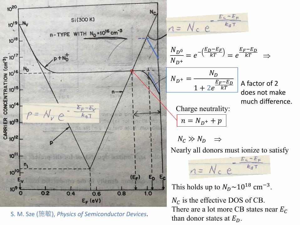
Charge neutrality:𝑛𝑛 = 𝑁𝑁𝐷𝐷+ + 𝑝𝑝
⇒
𝑁𝑁𝐷𝐷+ =𝑁𝑁𝐷𝐷
1 + 2𝑒𝑒𝐸𝐸𝐹𝐹−𝐸𝐸𝐷𝐷𝑘𝑘𝑘𝑘
𝑁𝑁𝐷𝐷0
𝑁𝑁𝐷𝐷+= 𝑒𝑒−
𝐸𝐸𝐷𝐷−𝐸𝐸𝐹𝐹𝑘𝑘𝑘𝑘 = 𝑒𝑒
𝐸𝐸𝐹𝐹−𝐸𝐸𝐷𝐷𝑘𝑘𝑘𝑘
𝑁𝑁𝐶𝐶 ≫ 𝑁𝑁𝐷𝐷 ⇒Nearly all donors must ionize to satisfy
This holds up to 𝑁𝑁𝐷𝐷~1018 cm−3.
𝑁𝑁𝐶𝐶 is the effective DOS of CB. There are a lot more CB states near 𝑑𝑑𝐶𝐶than donor states at 𝑑𝑑𝐷𝐷.
A factor of 2 does not make much difference.
S. M. Sze (施敏), Physics of Semiconductor Devices.
Increasing T
Decreasing T

ND
What is this shallow slope?
S. M. Sze (施敏), Physics of Semiconductor Devices.
Decrease T ⇒ 𝑑𝑑𝐶𝐶 > 𝑑𝑑𝐹𝐹 > 𝑑𝑑𝐷𝐷, similar to the intrinsic concentration:
The factor of 2 as in 𝑁𝑁𝐷𝐷+ =𝑁𝑁𝐷𝐷
1 + 2𝑒𝑒𝐸𝐸𝐹𝐹−𝐸𝐸𝐷𝐷𝑘𝑘𝑘𝑘
for RT.
𝑑𝑑𝐷𝐷
𝑑𝑑𝐶𝐶𝑑𝑑𝐷𝐷𝑏𝑏 𝑑𝑑𝐹𝐹
Grundmann, The Physics of Semiconductors, p. 216

p-type doping by shallow acceptors
𝑁𝑁𝐴𝐴 : acceptor concentration𝑁𝑁𝐴𝐴−: ionized acceptor concentration𝑁𝑁𝐴𝐴0: neutral acceptor concentration
At RT, essentially all acceptors are ionized, 𝑝𝑝 = 𝑁𝑁𝐴𝐴− = 𝑁𝑁𝐴𝐴
Grundmann, The Physics of Semiconductors, p. 209
p-type doping similar; flippedGrundmann, The Physics of Semiconductors, p. 219
Range in which typical electronics work

In the semiclassical model, ℏ𝑑𝑑𝑑𝑑𝑑𝑑𝑑𝑑
= ℏ𝑑𝑑𝑑𝑑𝑑𝑑
(𝑑𝑑 − 𝑑𝑑0) = 𝐹𝐹
𝑣𝑣𝑔𝑔 =1ℏ𝑑𝑑𝑑𝑑𝑑𝑑𝑑𝑑
=1ℏ
𝑑𝑑𝑑𝑑𝑑𝑑(𝑑𝑑 − 𝑑𝑑0)
Force on electron
The electron is pushed by the force to move in k-space. At each k, the electron’s velocity is the group velocity:
Question: Describe the motion of a single electron added to a perfect, static (T = 0) semiconductor crystal in a constant electric field.
Notice that 𝐯𝐯g = 0 at a minimum 𝐤𝐤 = 𝐤𝐤0.
𝐯𝐯g =1ℏ𝛻𝛻𝐤𝐤𝑑𝑑 =
1ℏ
�𝐱𝐱𝜕𝜕𝑑𝑑𝜕𝜕𝑑𝑑𝑥𝑥
+ �𝐲𝐲𝜕𝜕𝑑𝑑𝜕𝜕𝑑𝑑𝑦𝑦
+ �𝐳𝐳𝜕𝜕𝑑𝑑𝜕𝜕𝑑𝑑𝑧𝑧
𝑑𝑑𝐶𝐶The expected oscillation (called Bloch oscillation) is prevented by scattering, therefore has not been observed.
The static, perfect lattice does not scatter.
Charge transport
Collisions thermalize carriers, which thus remain near band extrema.
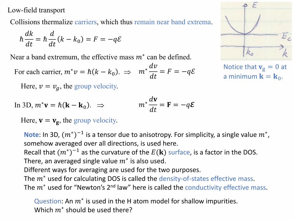
Low-field transport
Notice that 𝐯𝐯g = 0 at a minimum 𝐤𝐤 = 𝐤𝐤0.
Collisions thermalize carriers, which thus remain near band extrema.
Near a band extremum, the effective mass 𝑚𝑚∗ can be defined.
ℏ𝑑𝑑𝑑𝑑𝑑𝑑𝑑𝑑
= ℏ𝑑𝑑𝑑𝑑𝑑𝑑
𝑑𝑑 − 𝑑𝑑0 = 𝐹𝐹 = −𝑞𝑞ℰ
For each carrier, 𝑚𝑚∗𝑣𝑣 = ℏ 𝑑𝑑 − 𝑑𝑑0 . ⇒ 𝑚𝑚∗ 𝑑𝑑𝑣𝑣𝑑𝑑𝑑𝑑
= 𝐹𝐹 = −𝑞𝑞ℰ
Here, 𝑣𝑣 = 𝑣𝑣𝑔𝑔, the group velocity.
In 3D, 𝑚𝑚∗𝐯𝐯 = ℏ 𝐤𝐤 − 𝐤𝐤0 . ⇒ 𝑚𝑚∗ 𝑑𝑑𝐯𝐯𝑑𝑑𝑑𝑑
= 𝐅𝐅 = −𝑞𝑞𝓔𝓔
Here, 𝐯𝐯 = 𝐯𝐯𝐠𝐠, the group velocity.
Note: In 3D, (𝑚𝑚∗)−1 is a tensor due to anisotropy. For simplicity, a single value 𝑚𝑚∗, somehow averaged over all directions, is used here. Recall that (𝑚𝑚∗)−1 as the curvature of the 𝑑𝑑(𝐤𝐤) surface, is a factor in the DOS.There, an averaged single value 𝑚𝑚∗ is also used.Different ways for averaging are used for the two purposes. The 𝑚𝑚∗ used for calculating DOS is called the density-of-states effective mass. The 𝑚𝑚∗ used for “Newton’s 2nd law” here is called the conductivity effective mass.
Question: An 𝑚𝑚∗ is used in the H atom model for shallow impurities. Which 𝑚𝑚∗ should be used there?

Difference between metals and semiconductors in charge transport
Metals:𝑑𝑑𝐹𝐹 in partially occupied band.𝑓𝑓 𝑑𝑑 at RT deviates little from that at T = 0 due to large DOS in the band.
Non-degenerate semiconductors:𝑑𝑑𝐹𝐹 in gap. 𝑓𝑓 𝑑𝑑 at RT very different from that at T = 0. Very few electrons (compared to available states), thus Boltzmann distribution a good approximation to 𝑓𝑓 𝑑𝑑 . Mathematically, the tail to 𝑓𝑓 𝑑𝑑resembles Boltzmann distribution.

In electric field ℰ, each electron is shifted by Δ𝑑𝑑. Assuming energy-independent 𝜏𝜏, ℏΔ𝑑𝑑 = 𝑞𝑞ℰ𝜏𝜏.
In some metals, the nearly-free-electron model works well thus an 𝑚𝑚∗ (same as at the band bottom) can be defined for the electrons near 𝑑𝑑𝐹𝐹. Thus,
𝑚𝑚∗𝑣𝑣𝑑𝑑 = ℏΔ𝑑𝑑
𝑑𝑑𝐹𝐹
Equilibrium
∆k ∆k
In electric field ℰ
𝑑𝑑𝐹𝐹
In equilibrium, all electrons are inside the Fermi surface at T = 0. (A few excited out of it at T > 0.)If the Fermi surface is a sphere, what is the radius? Electrons on the Fermi surface move at 𝑣𝑣𝐹𝐹.
Metals
∆k∆kOnly a small portion of the electrons contribute to the net momentum, which is averaged by the total electron density n.
Question: When ℰ is very small, what is the average speedof those electrons contributing to the net momentum?

In some metals, the nearly-free-electron model works well thus an 𝑚𝑚∗ (same as at the band bottom) can be defined for the electrons near 𝑑𝑑𝐹𝐹. Thus,
∆k ∆k
In electric field ℰ
𝑑𝑑𝐹𝐹
∆k∆kWhen ℰ is very small, the average speed of those electrons contributing to the net momentum is ~ 𝑣𝑣𝐹𝐹.Therefore, the mean-free path is 𝑣𝑣𝐹𝐹𝜏𝜏.
Recall from Homework 4 that 𝑣𝑣𝐹𝐹 ~ 108 cm/s and 𝜏𝜏 ~ 10−14 s. Therefore, 𝑣𝑣𝐹𝐹𝜏𝜏 ~ 10−6 cm ~ 101 nm.
In these metals, 𝑚𝑚∗ ~ 𝑚𝑚0, the free electron mass.
Therefore, the Drude model works well: 1𝜌𝜌
= 𝜎𝜎 =𝑞𝑞2𝑛𝑛𝜏𝜏𝑚𝑚
With the correction that the mean-free path is 𝑣𝑣𝐹𝐹𝜏𝜏 (Drude-Sommerfeld model), it is a sufficient model for many metals in practical applications.
𝑚𝑚∗𝑣𝑣𝑑𝑑 = ℏΔ𝑑𝑑
https://slideplayer.com/slide/8690685/?

Semiconductors
A carrier behaves as a classical particle of mass 𝑚𝑚∗. Carriers follow Boltzmann distribution.Therefore, classical statistical mechanics works.
𝑚𝑚∗ 𝑑𝑑𝐯𝐯𝑑𝑑𝑑𝑑
= 𝐅𝐅 = −𝑞𝑞𝓔𝓔
The semiclassical model of semiconductors is similar to the Drude model:
In equilibrium or under low field, the average speedof carriers is the thermal velocity:
12𝑚𝑚∗𝑣𝑣𝑡𝑡ℎ2 =
32𝑑𝑑𝐵𝐵𝑇𝑇
At RT, 𝑣𝑣𝑡𝑡ℎ~107 cm/s.
If 𝜏𝜏 ~ 10−14 s, similar to those of metals, the mean free path 𝑣𝑣𝑡𝑡ℎ𝜏𝜏~10−7 cm = 100 nm.
Compare with metals: 𝑣𝑣𝐹𝐹 ~ 108 cm/s, thus mean free path 𝑣𝑣𝐹𝐹𝜏𝜏 ~ 10−6 cm ~ 101 nm.
Question: Given similar 𝜏𝜏, is a long mean free path good or bad for metals used as interconnects in modern ICs? (Hint: conductivity ∝ 𝜏𝜏.)

∆k∆kElectrons near Fermi surface move at speed 𝑣𝑣𝐹𝐹 in all directions. They travel longer between collisions if 𝑣𝑣𝐹𝐹 is larger.
Interconnects need to be thin and narrow. Collisions with surfaces lowers 𝜏𝜏 from the bulk value.
Grundmann, The Physics of Semiconductors, p. 824

Low-field transport in semiconductors
Notice that 𝐯𝐯g = 0 at a minimum 𝐤𝐤 = 𝐤𝐤0.
Collisions thermalize carriers, which thus remain near band extrema.
Near a band extremum, the effective mass 𝑚𝑚∗ can be defined.
ℏ𝑑𝑑𝑑𝑑𝑑𝑑𝑑𝑑
= ℏ𝑑𝑑𝑑𝑑𝑑𝑑
𝑑𝑑 − 𝑑𝑑0 = 𝐹𝐹 = −𝑞𝑞ℰ
For each carrier, 𝑚𝑚∗𝑣𝑣 = ℏ 𝑑𝑑 − 𝑑𝑑0 . ⇒ 𝑚𝑚∗ 𝑑𝑑𝑣𝑣𝑑𝑑𝑑𝑑
= 𝐹𝐹 = −𝑞𝑞ℰ
Here, 𝑣𝑣 = 𝑣𝑣𝑔𝑔, the group velocity.
In 3D, 𝑚𝑚∗𝐯𝐯 = ℏ 𝐤𝐤 − 𝐤𝐤0 . ⇒ 𝑚𝑚∗ 𝑑𝑑𝐯𝐯𝑑𝑑𝑑𝑑
= 𝐅𝐅 = −𝑞𝑞𝓔𝓔
Here, 𝐯𝐯 = 𝐯𝐯𝐠𝐠, the group velocity.
𝐯𝐯d = −𝑞𝑞𝓔𝓔𝜏𝜏𝑚𝑚∗ Define mobility 𝜇𝜇 =
𝑞𝑞𝜏𝜏𝑚𝑚∗ ⇒ 𝐯𝐯d = − 𝑞𝑞𝜇𝜇𝓔𝓔
1𝜌𝜌
= 𝜎𝜎 =𝑞𝑞2𝑛𝑛𝜏𝜏𝑚𝑚∗ = 𝑞𝑞𝑛𝑛𝜇𝜇𝐉𝐉 = −𝑛𝑛𝑞𝑞𝐯𝐯d =
𝑞𝑞2𝑛𝑛𝜏𝜏𝑚𝑚∗ 𝓔𝓔 ⇒
Consider both electrons and holes: 𝜎𝜎 = 𝑞𝑞𝑛𝑛𝜇𝜇𝑒𝑒 + 𝑞𝑞𝑝𝑝𝜇𝜇ℎ

𝐯𝐯d = −𝑞𝑞𝓔𝓔𝜏𝜏𝑚𝑚∗
Define mobility 𝜇𝜇 =𝑞𝑞𝜏𝜏𝑚𝑚∗ ⇒ 𝐯𝐯d = − 𝑞𝑞𝜇𝜇𝓔𝓔
1𝜌𝜌
= 𝜎𝜎 =𝑞𝑞2𝑛𝑛𝜏𝜏𝑚𝑚∗ = 𝑞𝑞𝑛𝑛𝜇𝜇
𝐉𝐉 = −𝑛𝑛𝑞𝑞𝐯𝐯d =𝑞𝑞2𝑛𝑛𝜏𝜏𝑚𝑚∗ 𝓔𝓔
⇒
Consider both electrons and holes:𝜎𝜎 = 𝑞𝑞𝑛𝑛𝜇𝜇𝑒𝑒 + 𝑞𝑞𝑝𝑝𝜇𝜇ℎ
This formulation gives us the impression that the mobilities are a sort of materials property of semiconductors.
Many textbooks list 𝜇𝜇𝑒𝑒 = 1500 ⁄cm2 (Vs)and 𝜇𝜇ℎ = 450 ⁄cm2 (Vs) without much explanation.
But, you probably have never seen such high values in simulation models or lab measurements. Let’s look at some data.
Yu & Cardona, Fundamentals of Semiconductors, 4th Ed. p. 222

Carrier may collide with, or be scattered by, multiple types of scatterers. Scattering processes/mechanisms
Each scattering process/mechanism has its own signature 𝜏𝜏 or 𝜇𝜇 dependence on temperature T and carrier density n or p.
𝜇𝜇 =𝑞𝑞𝜏𝜏𝑚𝑚∗
𝜇𝜇𝑖𝑖 =𝑞𝑞𝜏𝜏𝑖𝑖𝑚𝑚∗
The more frequently carriers are scattered, the lower the mobility.
Different scattering processes have different contributions to the total scattering rate:
1𝜏𝜏
= �𝑖𝑖
1𝜏𝜏𝑖𝑖
The scattering rate or frequency due to the ith process/mechanism
We can then assign thus1𝜇𝜇
= �𝑖𝑖
1𝜇𝜇𝑖𝑖
By measuring the dependence of 𝜇𝜇 on T, n or p, and parameters related to the scattering processes, we can find which processes are the major ones.
Mobility 𝜇𝜇 and scattering time 𝜏𝜏 describe the overall effect of allscattering processes/mechanisms due to multiple types of scatterers.
The total scattering rate is a simple sum of rates of individual processes if the processes are independent of each other.

Analysis of individual scattering processes/mechanisms for T and n (or p) dependence
𝐯𝐯d = −𝑞𝑞𝓔𝓔𝜏𝜏𝑚𝑚∗ Define mobility 𝜇𝜇 =
𝑞𝑞𝜏𝜏𝑚𝑚∗ ⇒ 𝐯𝐯d = − 𝑞𝑞𝜇𝜇𝓔𝓔
1𝜌𝜌
= 𝜎𝜎 =𝑞𝑞2𝑛𝑛𝜏𝜏𝑚𝑚∗ = 𝑞𝑞𝑛𝑛𝜇𝜇𝐉𝐉 = −𝑛𝑛𝑞𝑞𝐯𝐯d =
𝑞𝑞2𝑛𝑛𝜏𝜏𝑚𝑚∗ 𝓔𝓔 ⇒
So far we have assumed all electrons have the same scattering time 𝜏𝜏:
If this were true, then 𝜇𝜇 would be independent of T and be less sensitive to n (or p).
When the energy-dependent scattering time 𝜏𝜏(𝑑𝑑) is considered, we replace 𝜏𝜏 in the above equations with average scattering time 𝜏𝜏 , so that they still hold.
(Or, we simply write 𝜏𝜏 but interpret it as 𝜏𝜏 .)
The analysis and the averaging procedure is complicated. We just describe the big picture.
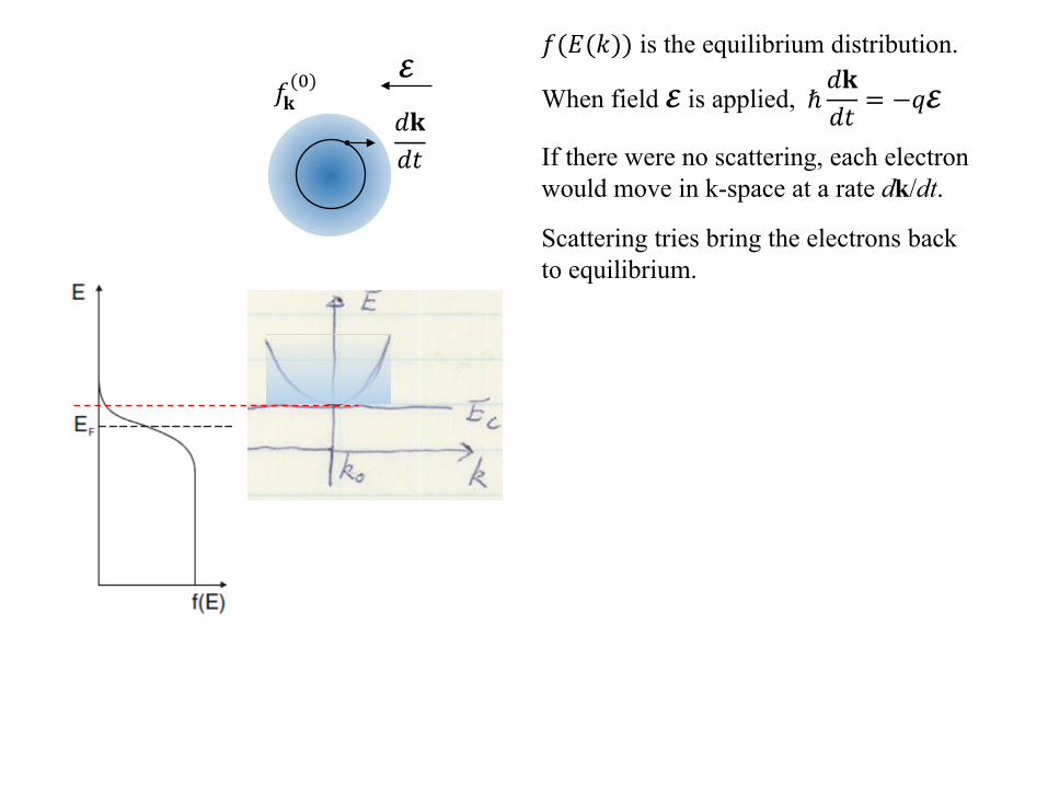
𝑓𝑓𝐤𝐤(0)
𝑓𝑓(𝑑𝑑(𝑑𝑑)) is the equilibrium distribution.
When field 𝓔𝓔 is applied, ℏ𝑑𝑑𝐤𝐤𝑑𝑑𝑑𝑑
= −𝑞𝑞𝓔𝓔𝑑𝑑𝐤𝐤𝑑𝑑𝑑𝑑 If there were no scattering, each electron
would move in k-space at a rate dk/dt.
𝓔𝓔
Scattering tries bring the electrons back to equilibrium.

𝑓𝑓𝐤𝐤(0)
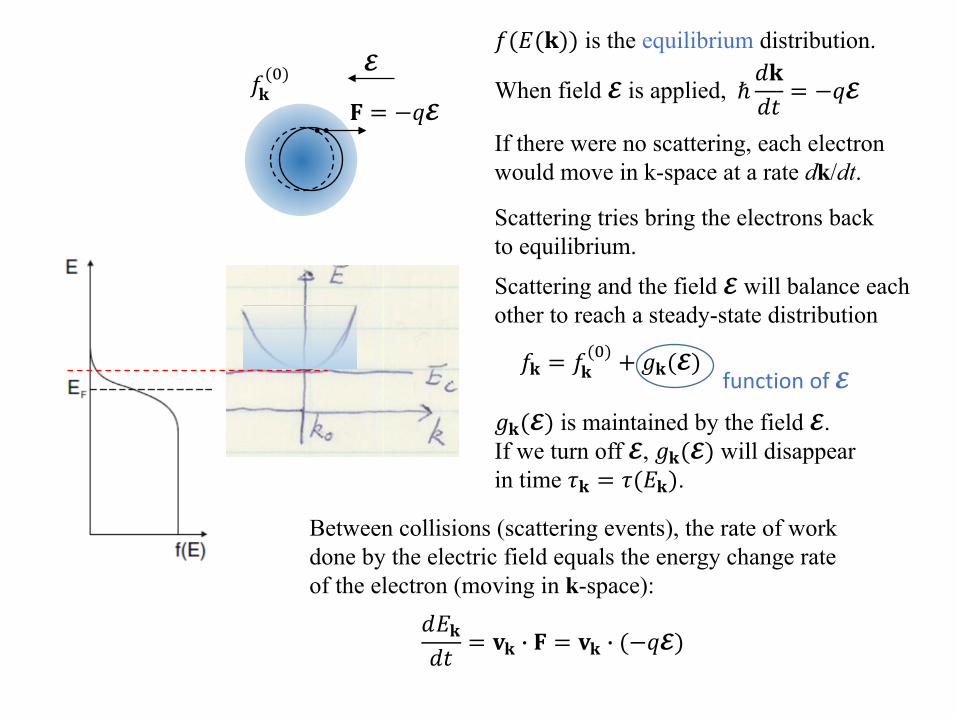
𝑓𝑓(𝑑𝑑(𝐤𝐤)) is the equilibrium distribution.
When field 𝓔𝓔 is applied, ℏ𝑑𝑑𝐤𝐤𝑑𝑑𝑑𝑑
= −𝑞𝑞𝓔𝓔
If there were no scattering, each electron would move in k-space at a rate dk/dt.
𝓔𝓔
Scattering tries bring the electrons back to equilibrium.
Scattering and the field 𝓔𝓔 will balance each other to reach a steady-state distribution
𝑓𝑓𝐤𝐤 = 𝑓𝑓𝐤𝐤(0) + 𝑔𝑔𝐤𝐤(𝓔𝓔)
function of 𝓔𝓔
𝑔𝑔𝐤𝐤(𝓔𝓔) is maintained by the field 𝓔𝓔. If we turn off 𝓔𝓔, 𝑔𝑔𝐤𝐤(𝓔𝓔) will disappear in time 𝜏𝜏𝐤𝐤 = 𝜏𝜏(𝑑𝑑𝐤𝐤). For this reason, 𝜏𝜏 is also called the relaxation time.
Here, 𝑓𝑓𝐤𝐤 is the probability that that the state at k is occupied, and 𝑓𝑓𝐤𝐤
(0) is the equilibrium value of 𝑓𝑓𝐤𝐤.
𝑓𝑓𝐤𝐤(0) = 𝑓𝑓(𝑑𝑑(𝐤𝐤)) = 𝑓𝑓(𝑑𝑑𝐤𝐤)
𝑓𝑓𝐤𝐤(0)
𝑓𝑓(𝑑𝑑(𝐤𝐤)) is the equilibrium distribution.
When field 𝓔𝓔 is applied, ℏ𝑑𝑑𝐤𝐤𝑑𝑑𝑑𝑑
= −𝑞𝑞𝓔𝓔
If there were no scattering, each electron would move in k-space at a rate dk/dt.
𝓔𝓔
Scattering tries bring the electrons back to equilibrium.
Scattering and the field 𝓔𝓔 will balance each other to reach a steady-state distribution
𝑓𝑓𝐤𝐤 = 𝑓𝑓𝐤𝐤(0) + 𝑔𝑔𝐤𝐤(𝓔𝓔)
function of 𝓔𝓔
𝑔𝑔𝐤𝐤(𝓔𝓔) is maintained by the field 𝓔𝓔. If we turn off 𝓔𝓔, 𝑔𝑔𝐤𝐤(𝓔𝓔) will disappear in time 𝜏𝜏𝐤𝐤 = 𝜏𝜏(𝑑𝑑𝐤𝐤).
𝐅𝐅 = −𝑞𝑞𝓔𝓔
Between collisions (scattering events), the rate of workdone by the electric field equals the energy change rate of the electron (moving in k-space):
𝑑𝑑𝑑𝑑𝐤𝐤𝑑𝑑𝑑𝑑
= 𝐯𝐯𝐤𝐤 � 𝐅𝐅 = 𝐯𝐯𝐤𝐤 � (−𝑞𝑞𝓔𝓔)

𝑓𝑓𝐤𝐤(0)
𝑓𝑓(𝑑𝑑(𝐤𝐤)) is the equilibrium distribution.
When field 𝓔𝓔 is applied, ℏ𝑑𝑑𝐤𝐤𝑑𝑑𝑑𝑑
= −𝑞𝑞𝓔𝓔
If there were no scattering, each electron would move in k-space at a rate dk/dt.
𝓔𝓔
Scattering tries bring the electrons back to equilibrium.
Scattering and the field 𝓔𝓔 will balance each other to reach a steady-state distribution
𝑓𝑓𝐤𝐤 = 𝑓𝑓𝐤𝐤(0) + 𝑔𝑔𝐤𝐤(𝓔𝓔)
function of 𝓔𝓔
𝑔𝑔𝐤𝐤(𝓔𝓔) is maintained by the field 𝓔𝓔. If we turn off 𝓔𝓔, 𝑔𝑔𝐤𝐤(𝓔𝓔) will disappear in time 𝜏𝜏𝐤𝐤 = 𝜏𝜏(𝑑𝑑𝐤𝐤).
𝐅𝐅 = −𝑞𝑞𝓔𝓔
Work done by 𝓔𝓔 changes electron energy: 𝑑𝑑𝑑𝑑𝐤𝐤𝑑𝑑𝑑𝑑
= 𝐯𝐯𝐤𝐤 � 𝐅𝐅 = −𝑞𝑞𝐯𝐯𝐤𝐤 � 𝓔𝓔
Thus, field 𝓔𝓔 attempts to change distribution 𝑓𝑓𝐤𝐤 at a rate:𝑑𝑑𝑓𝑓𝐤𝐤𝑑𝑑𝑑𝑑 field
≈𝜕𝜕𝑓𝑓𝐤𝐤
(0)
𝜕𝜕𝑑𝑑𝐤𝐤𝑑𝑑𝑑𝑑𝐤𝐤𝑑𝑑𝑑𝑑
= −𝜕𝜕𝑓𝑓𝐤𝐤
(0)
𝜕𝜕𝑑𝑑𝐤𝐤𝑞𝑞𝐯𝐯𝐤𝐤 � 𝓔𝓔
Valid for small 𝓔𝓔

𝑓𝑓𝐤𝐤(0)
𝑓𝑓(𝑑𝑑(𝐤𝐤)) is the equilibrium distribution. 𝓔𝓔
Scattering and the field 𝓔𝓔 will balance each other to reach a steady-state distribution
𝑓𝑓𝐤𝐤 = 𝑓𝑓𝐤𝐤(0) + 𝑔𝑔𝐤𝐤(𝓔𝓔)
function of 𝓔𝓔
𝑔𝑔𝐤𝐤(𝓔𝓔) is maintained by the field 𝓔𝓔. If we turn off 𝓔𝓔, 𝑔𝑔𝐤𝐤(𝓔𝓔) will disappear in time 𝜏𝜏𝐤𝐤 = 𝜏𝜏(𝑑𝑑𝐤𝐤).
𝐅𝐅 = −𝑞𝑞𝓔𝓔
Work done by 𝓔𝓔 changes electron energy:𝑑𝑑𝑑𝑑𝐤𝐤𝑑𝑑𝑑𝑑
= 𝐯𝐯𝐤𝐤 � 𝐅𝐅 = −𝑞𝑞𝐯𝐯𝐤𝐤 � 𝓔𝓔
Thus, field 𝓔𝓔 attempts to change distribution 𝑓𝑓𝐤𝐤 at a rate:
𝑑𝑑𝑓𝑓𝐤𝐤𝑑𝑑𝑑𝑑 field
≈𝜕𝜕𝑓𝑓𝐤𝐤
(0)
𝜕𝜕𝑑𝑑𝐤𝐤𝑑𝑑𝑑𝑑𝐤𝐤𝑑𝑑𝑑𝑑
= −𝜕𝜕𝑓𝑓𝐤𝐤
(0)
𝜕𝜕𝑑𝑑𝐤𝐤𝑞𝑞𝐯𝐯𝐤𝐤 � 𝓔𝓔
The change accrued in time 𝜏𝜏𝐤𝐤 is 𝑔𝑔𝐤𝐤(𝓔𝓔): 𝑔𝑔𝐤𝐤(𝓔𝓔) =𝑑𝑑𝑓𝑓𝐤𝐤𝑑𝑑𝑑𝑑 field
𝜏𝜏𝐤𝐤 = −𝜕𝜕𝑓𝑓𝐤𝐤
(0)
𝜕𝜕𝑑𝑑𝐤𝐤𝑞𝑞𝜏𝜏𝐤𝐤𝐯𝐯𝐤𝐤 � 𝓔𝓔

𝑓𝑓𝐤𝐤(0)
𝑓𝑓(𝑑𝑑(𝐤𝐤)) is the equilibrium distribution. 𝓔𝓔
Scattering and the field 𝓔𝓔 will balance each other to reach a steady-state distribution
𝑓𝑓𝐤𝐤 = 𝑓𝑓𝐤𝐤(0) + 𝑔𝑔𝐤𝐤(𝓔𝓔)
function of 𝓔𝓔
𝐅𝐅 = −𝑞𝑞𝓔𝓔
The field 𝓔𝓔 attempts to change 𝑓𝑓𝐤𝐤 at a rate
𝑑𝑑𝑓𝑓𝐤𝐤𝑑𝑑𝑑𝑑 field
= −𝜕𝜕𝑓𝑓𝐤𝐤
(0)
𝜕𝜕𝑑𝑑𝐤𝐤𝑞𝑞𝐯𝐯𝐤𝐤 � 𝓔𝓔
The change accrued in time 𝜏𝜏𝐤𝐤 is 𝑔𝑔𝐤𝐤(𝓔𝓔):
𝑔𝑔𝐤𝐤(𝓔𝓔) =𝑑𝑑𝑓𝑓𝐤𝐤𝑑𝑑𝑑𝑑 field
𝜏𝜏𝐤𝐤 = −𝜕𝜕𝑓𝑓𝐤𝐤
(0)
𝜕𝜕𝑑𝑑𝐤𝐤𝑞𝑞𝜏𝜏𝐤𝐤𝐯𝐯𝐤𝐤 � 𝓔𝓔
(which is relaxed/eliminated by scattering)
The current density is: 𝐉𝐉 = �𝑞𝑞𝑓𝑓𝐤𝐤𝐯𝐯𝐤𝐤𝑑𝑑3𝐤𝐤 Integral over entire k-space
�𝑞𝑞𝑓𝑓𝐤𝐤(0)𝐯𝐯𝐤𝐤𝑑𝑑3𝐤𝐤 = 0
No current in equilibrium
⇒ 𝐉𝐉 = �𝑞𝑞𝑔𝑔𝐤𝐤𝐯𝐯𝐤𝐤𝑑𝑑3𝐤𝐤 = −𝑞𝑞2 �𝜕𝜕𝑓𝑓𝐤𝐤
0
𝜕𝜕𝑑𝑑𝐤𝐤(𝐯𝐯𝐤𝐤 � 𝓔𝓔 )𝜏𝜏𝐤𝐤𝐯𝐯𝐤𝐤𝑑𝑑3𝐤𝐤

𝑓𝑓𝐤𝐤(0)
𝑓𝑓𝐤𝐤(0) = 𝑓𝑓(𝑑𝑑(𝐤𝐤)) is the equilibrium distribution.
𝓔𝓔
𝑓𝑓𝐤𝐤 = 𝑓𝑓𝐤𝐤(0) + 𝑔𝑔𝐤𝐤(𝓔𝓔)
function of 𝓔𝓔
𝐅𝐅 = −𝑞𝑞𝓔𝓔
The field 𝓔𝓔 attempts to change 𝑓𝑓𝐤𝐤, while scattering attempts to eliminate the change. A balance is reached at a steady-state distribution
The change driven by the field accrued in time 𝜏𝜏𝐤𝐤 is 𝑔𝑔𝐤𝐤(𝓔𝓔), to be relaxed/eliminated by scattering:
𝑔𝑔𝐤𝐤(𝓔𝓔) = −𝜕𝜕𝑓𝑓𝐤𝐤
(0)
𝜕𝜕𝑑𝑑𝐤𝐤𝑞𝑞𝜏𝜏𝐤𝐤𝐯𝐯𝐤𝐤 � 𝓔𝓔
Net current is due to 𝑔𝑔𝐤𝐤(𝓔𝓔):
𝐉𝐉 = �𝑞𝑞𝑔𝑔𝐤𝐤𝐯𝐯𝐤𝐤𝑑𝑑3𝐤𝐤 = −𝑞𝑞2 �𝜕𝜕𝑓𝑓𝐤𝐤
0
𝜕𝜕𝑑𝑑𝐤𝐤(𝐯𝐯𝐤𝐤 � 𝓔𝓔 )𝜏𝜏𝐤𝐤𝐯𝐯𝐤𝐤𝑑𝑑3𝐤𝐤
𝑓𝑓𝐤𝐤(0) = 𝑓𝑓(𝑑𝑑(𝐤𝐤)) is approximately Boltzmann for nondegenerate semiconductors.
Use DOS to convert the integral over 𝑑𝑑3𝐤𝐤 to one over 2𝜋𝜋𝑑𝑑2 ⁄𝑑𝑑𝑑𝑑 𝑑𝑑𝑑𝑑 𝑑𝑑𝑑𝑑, then

𝜎𝜎 =𝑞𝑞2𝑛𝑛 𝜏𝜏𝑚𝑚∗We want a single value, the average scattering time 𝜏𝜏 , so that
Therefore, the average scattering time 𝜏𝜏 is: 𝜏𝜏 =𝑚𝑚∗
𝑞𝑞2𝜎𝜎𝑛𝑛
Insert Eq. (5.25)
𝑛𝑛 = �𝐷𝐷 𝑑𝑑 𝑓𝑓 𝑑𝑑 𝑑𝑑𝑑𝑑
𝐷𝐷 𝑑𝑑 ∝ 𝑑𝑑
Slides 49 to 56 (this one) explain Sections 5.2.1 & 5.2.2 of Yu & Cardona, Fundamentals of Semiconductors. Books on advanced topics in semiconductors are often very dense, not easy to read. The field is vast, thus cannot be covered by a single course. You are encourage to read the two sections, and learn how to learn by reading on your own. This content is in many textbooks. There are often small errors (especially signs), but they all end up with the right results (two wrongs make it right).
Once we know 𝜏𝜏(𝑑𝑑), we apply Eq. (5.27) find 𝜏𝜏 and thus get its dependence on T and n (or p). Since 𝜇𝜇 ∝ 𝜏𝜏 , 𝜇𝜇 has the same dependence. Next, we show this with one important scattering mechanism.

Yu & Cardona, Fundamentals of Semiconductors, 4th Ed. p. 218
Charged impurity scattering
Conwell-Weisskopf (CW) approach: Classical treatment in the same manner as Rutherford scattering.
Impurity concentration, i for ionized impurity. If all ions are ionized shallow donors, 𝑁𝑁𝑖𝑖 = 𝑛𝑛.
The take-home message is 1
𝜏𝜏i(𝑑𝑑𝑘𝑘)∝ 𝑛𝑛𝑑𝑑𝑘𝑘
− ⁄3 2.
Weak dependence to be neglected
Overall, 𝜇𝜇i ∝ 𝜏𝜏i ∝ 𝑛𝑛− ⁄2 3
Brooks-Herring (BH) approach: Quantum mechanical treatment, yielding very similar results.

Charged impurity scattering: carrier concentration dependence
Yu & Cardona, Fundamentals of Semiconductors, 4th Ed. p. 220
𝜇𝜇i ∝ 𝜏𝜏i ∝ 𝑛𝑛− ⁄2 3
Notice the very high values!
For 𝑁𝑁𝐷𝐷 ~ 1016 cm−3, ion-scattering-limited mobility 𝜇𝜇i ~ 105 ⁄cm2 (Vs)

Charged impurity scattering: temperature dependence
If 𝜏𝜏(𝑑𝑑) ∝ 𝑑𝑑𝑛𝑛𝑇𝑇𝑚𝑚,
For charged impurity scattering,
Therefore, n = 3/2 and m = 0.
1𝜏𝜏i(𝑑𝑑𝑘𝑘)
∝ 𝑛𝑛𝑒𝑒𝑑𝑑𝑘𝑘− ⁄3 2.
⇒ 15002000
3000
×2
×2
1𝜏𝜏
= �𝑖𝑖
1𝜏𝜏𝑖𝑖
Recall that
1𝜇𝜇
= �𝑖𝑖
1𝜇𝜇𝑖𝑖
1𝜇𝜇
= �𝑖𝑖
1𝜇𝜇𝑖𝑖
And, for 𝑁𝑁𝐷𝐷 ~ 1016 cm−3, ion-scattering-limited mobility 𝜇𝜇i~ 105 ⁄cm2 (Vs) at 300 K. (See previous slide.)There must be another mechanism that dominates.
Electron concentration

Phonon scattering
15002000
3000
×2
×2
1𝜇𝜇
= �𝑖𝑖
1𝜇𝜇𝑖𝑖
In ionized impurity scattering, the carrier is scattered by a static potential. The carrier’s momentum is randomized, but it does not loose any energy. Such a scattering event is elastic.
A carrier may be bounced by the vibrating lattice, exchanging momentum and energy with the vibration modes.
Normal modes of coupled harmonicoscillators: A system of coupledharmonic oscillators with N degrees of freedom has N normal modes of oscillation, equivalent to N independentoscillators.
A crystal in 3D made of N atoms is approximated by coupled harmonic oscillator system with 3N degrees of freedom: 3N normal modes, equivalent to 3N independent oscillators.

A system of coupled harmonic oscillators with N degrees of freedom has N normal modes of oscillation, equivalent to Nindependent oscillators.
A simple example:
2 degrees of freedom, 2 normal modes with 2 frequenciesIntuitive way to look at the two modes:
Two masses move in phase: 𝜔𝜔1 =𝑑𝑑1𝑚𝑚
𝜔𝜔2 =𝑑𝑑1 + 2𝑑𝑑2
𝑚𝑚
For details, visit: http://sites.science.oregonstate.edu/~roundyd/COURSES/ph427/two-coupled-oscillators.html
For visualization, see video: https://www.youtube.com/watch?v=x_ZkKPtgTeA
2𝑑𝑑1
2m𝑑𝑑1
𝑑𝑑1
2m𝑑𝑑1 + 2𝑑𝑑2
=
=
The normal modes are also called eigenmodes, and the two frequencies are eigenvalues.
Notice the same math as in quantum mechanics. What if we start the oscillation by pulling only one while holding the other and than release both?
Two masses move out of phase:

Imagine we have a network of masses connected by springs:
This drawing is in 1D. Use your imagination for 3DEquilibrium position
If we a flying object hits one mass, displacing it and starting the vibration, the vibration will propagate throughout the network – sound wave.
But this sound wave is different from a sound wave in a continuous medium:the masses are discrete.
Still remember aliasing? Watch animation at https://en.wikipedia.org/wiki/File:Phonon_k_3k.gif
a
aλ = 2a
Wavelength or wavevector aliasing:In a lattice of lattice parameter a,two waves with wavevectors k and 𝑑𝑑 + 2𝑛𝑛𝜋𝜋 are indistinguishable.
Take-home exercise: Show that in the animation the two waves (black & red) satisfy the aliasing condition.

Equilibrium positiona
Vibration will propagate throughout the network, just as in a continuous medium – sound wave:
𝑢𝑢𝑛𝑛
𝑢𝑢𝑛𝑛 = Re 𝐴𝐴𝑒𝑒𝑘𝑘𝑛𝑛𝑘𝑘−𝑖𝑖𝜔𝜔𝑡𝑡
Grundmann, The Physics of Semiconductors, p. 114
Solve difference equations based on Hooke's law, applying periodic condition 𝑢𝑢𝑁𝑁+1 = 𝑢𝑢1.
In a continuous medium, solve differential equations, with Young's modulus in place of the spring constant.
For long waves, small wavevectors k, λ ≫ 𝑎𝑎, as if the chain is a continuous string. The speed of the sound wave ⁄𝜔𝜔 𝑑𝑑 ≈ ⁄𝑑𝑑𝜔𝜔 𝑑𝑑𝑑𝑑
𝜔𝜔 =4𝐾𝐾𝑀𝑀
sin𝑑𝑑𝑎𝑎2
Compare to the Bloch wave of electrons. The electron de Broglie wave in free space is parabolic.
K
M
N masses, if confined in 1D, N degrees of freedom. N distinguishable k values, N modes.
𝑢𝑢𝑁𝑁+1 = 𝑢𝑢1, 𝑢𝑢𝑛𝑛 = 𝑢𝑢𝑛𝑛+𝑁𝑁 ⇒ 𝑑𝑑𝑁𝑁𝑎𝑎 = 2𝑙𝑙𝜋𝜋 𝑑𝑑 = 𝑙𝑙2𝜋𝜋𝑁𝑁𝑎𝑎
= 𝑙𝑙2𝜋𝜋𝐿𝐿
i.e.
l being integers, −N/2 < l ≤ N/2

Equilibrium positiona
𝑢𝑢𝑛𝑛
K
M
𝑢𝑢𝑛𝑛 = Re 𝐴𝐴𝑒𝑒𝑘𝑘𝑛𝑛𝑘𝑘−𝑖𝑖𝜔𝜔𝑡𝑡 𝜔𝜔 =4𝐾𝐾𝑀𝑀
sin𝑑𝑑𝑎𝑎2
N Masses, if confined in 1D, N degrees of freedom. N distinguishable k values, N modes.
𝑑𝑑 = 𝑙𝑙2𝜋𝜋𝑁𝑁𝑎𝑎
= 𝑙𝑙2𝜋𝜋𝐿𝐿
in the fist BZ.
This is the simplest model of lattice vibration.
But, why can we model atoms in a lattice by masses connected by springs?
𝑯𝑯ψ 𝐫𝐫𝑖𝑖 , {𝐑𝐑𝑗𝑗} = 𝑑𝑑ψ 𝐫𝐫𝑖𝑖 , {𝐑𝐑𝑗𝑗}
𝐩𝐩𝑖𝑖 = −𝑖𝑖ℏ𝛻𝛻𝑖𝑖𝐏𝐏𝑗𝑗 = −𝑖𝑖ℏ𝛻𝛻𝑗𝑗Each 3D.
Recall that we are not able to solve this for ~1023 variables:

So we invoke the Born-Oppenheimer approximation:Consider fixed nuclei. Solve Schrödinger equations for varied fixed nuclear positions, and then handle nuclear motion later. Justification: proton to electron mass ratio = 1836
The electron Hamiltonian
e-e interaction electron-nucleus Coulomb interactionelectron kinetic energy
Notice that this is not separation of variables.
The electronic equations ℋ𝑒𝑒ψ𝑒𝑒 𝐫𝐫𝑖𝑖 ; {𝐑𝐑𝑗𝑗} = E𝑒𝑒𝑐𝑐 {𝐑𝐑𝑗𝑗} ψ𝑒𝑒 𝐫𝐫𝑖𝑖 ; {𝐑𝐑𝑗𝑗} are solved with {𝐑𝐑𝑗𝑗} as parameters.
Then, electron-core energy E𝑒𝑒𝑐𝑐 {𝐑𝐑𝑗𝑗} , the ground state eigen energy of the electronic equation, is used as part of the potential to solve the ion Hamiltonian.(see next slide)
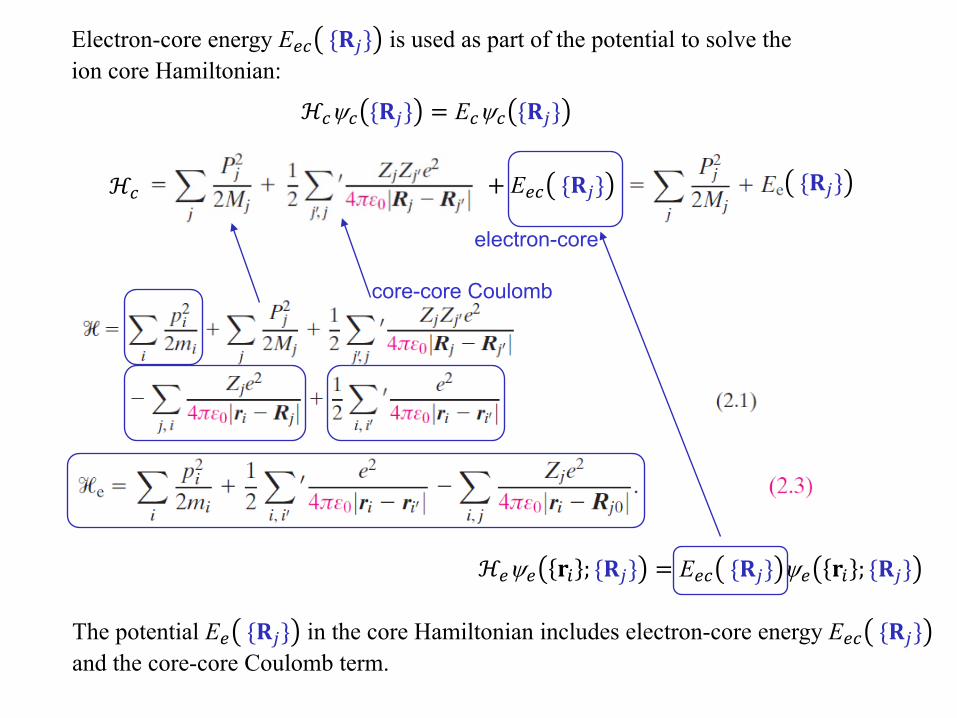
Electron-core energy E𝑒𝑒𝑐𝑐 {𝐑𝐑𝑗𝑗} is used as part of the potential to solve the ion core Hamiltonian:
ℋ𝑐𝑐ψ𝑐𝑐 {𝐑𝐑𝑗𝑗} = E𝑐𝑐ψ𝑐𝑐 {𝐑𝐑𝑗𝑗}
ℋ𝑐𝑐 + E𝑒𝑒𝑐𝑐 {𝐑𝐑𝑗𝑗} {𝐑𝐑𝑗𝑗}
ℋ𝑒𝑒ψ𝑒𝑒 𝐫𝐫𝑖𝑖 ; {𝐑𝐑𝑗𝑗} = E𝑒𝑒𝑐𝑐 {𝐑𝐑𝑗𝑗} ψ𝑒𝑒 𝐫𝐫𝑖𝑖 ; {𝐑𝐑𝑗𝑗}
electron-core
core-core Coulomb
The potential E𝑒𝑒 {𝐑𝐑𝑗𝑗} in the core Hamiltonian includes electron-core energy E𝑒𝑒𝑐𝑐 {𝐑𝐑𝑗𝑗}and the core-core Coulomb term.

Simple example to illustrate this procedure: H2 molecule
First, calculate the electronic energy E𝑒𝑒 𝑅𝑅 by solving
http://www.tcm.phy.cam.ac.uk/~bds10/aqp/lec15.pdf
https://chemistry.stackexchange.com/questions/99852/hydrogen-molecule-potential-energy-graph
ℋ𝑒𝑒ψ𝑒𝑒 𝐫𝐫1, 𝐫𝐫2;𝑅𝑅 = E𝑒𝑒𝑐𝑐 𝑅𝑅 ψ𝑒𝑒 𝐫𝐫1, 𝐫𝐫2;𝑅𝑅For many values of 𝑅𝑅 (𝑅𝑅 being a parameter).
E𝑒𝑒 𝑅𝑅 =𝑒𝑒2
4𝜋𝜋𝜀𝜀0𝑅𝑅2+ E𝑒𝑒𝑐𝑐 𝑅𝑅
nuclear-nuclear Coulomb
elementary charge
E𝑒𝑒 𝑅𝑅
𝑅𝑅
First, use the electronic energy E𝑒𝑒 𝑅𝑅 as the potential to solve
ℋ𝑐𝑐ψ𝑐𝑐 𝑅𝑅 = E𝑐𝑐ψ𝑐𝑐 𝑅𝑅
ℋ𝑐𝑐 =𝑃𝑃2
𝑀𝑀+ E𝑒𝑒 𝑅𝑅
𝑃𝑃 = −𝑖𝑖ℏ𝑑𝑑𝑑𝑑𝑅𝑅
𝑅𝑅 is the variable here in the nuclear equation.
Harmonic approximation:Near equilibrium, the curve is approximated by 𝐾𝐾𝑅𝑅2/2.
ground state energy of electronic equation for R
Operator

https://courses.lumenlearning.com/trident-boundless-chemistry/chapter/bond-energy-and-enthalpy/
Harmonic approximation:Near equilibrium, the curve is approximated by 𝐾𝐾𝑅𝑅2/2.
E𝑒𝑒 𝑅𝑅
𝑅𝑅
𝑅𝑅
equilibrium
𝜔𝜔 =𝐾𝐾𝑀𝑀
The H2 molecule can be modeled as a simple harmonic oscillator:
Vibrational energy levels:
𝑑𝑑𝑐𝑐(𝜈𝜈) = 𝜈𝜈 +
12
ℏ𝜔𝜔
𝜈𝜈 = 0, 1, 2, …
Notice that even for 𝜈𝜈 = 0, the vibrational energy is not zero:
𝑑𝑑𝑐𝑐(0) =
12ℏ𝜔𝜔
(Zero point energy)
Even at T = 0, this is the lowest energy of the H2 molecule.

The electron Hamiltonian
e-e interaction electron-nucleus Coulomb interactionelectron kinetic energy
Solving the electronic equations ℋ𝑒𝑒ψ𝑒𝑒 𝐫𝐫𝑖𝑖 ; {𝐑𝐑𝑗𝑗} = E𝑒𝑒𝑐𝑐 {𝐑𝐑𝑗𝑗} ψ𝑒𝑒 𝐫𝐫𝑖𝑖 ; {𝐑𝐑𝑗𝑗} with {𝐑𝐑𝑗𝑗} as parameters yields ground state electron-core energy E𝑒𝑒𝑐𝑐 {𝐑𝐑𝑗𝑗} , in principle.
The function E𝑒𝑒 {𝐑𝐑𝑗𝑗} is represented by a hypersurface in the high-dimensionality configuration space {𝐑𝐑𝑗𝑗},
Now, back to our crystalline solids.
+ E𝑒𝑒𝑐𝑐 {𝐑𝐑𝑗𝑗}
core-core Coulomb
E𝑒𝑒 {𝐑𝐑𝑗𝑗} =
Then, it is trivial to find the “potential” E𝑒𝑒 {𝐑𝐑𝑗𝑗} :
in comparison with E𝑒𝑒 𝑅𝑅 of H2, represented by a curve of one variable 𝑅𝑅.
There are ~1023 atomic positions in {𝐑𝐑𝑗𝑗}, and each 𝐑𝐑𝑗𝑗 is 3D. The configuration space {𝐑𝐑𝑗𝑗} is indeed very high-dimensional! The hypersurface E𝑒𝑒 {𝐑𝐑𝑗𝑗} is referred to as the “energy landscape” by some.
A minimum of hypersurface E𝑒𝑒 {𝐑𝐑𝑗𝑗} is located at a configuration {𝐑𝐑𝑗𝑗0}, corresponding to the crystal structure to be studied.

In principle, solving the ion core (vibration) equation ℋ𝑐𝑐ψ𝑐𝑐 {𝐑𝐑𝑗𝑗} = E𝑐𝑐ψ𝑐𝑐 {𝐑𝐑𝑗𝑗}
ℋ𝑐𝑐 {𝐑𝐑𝑗𝑗} ,
yields vibrational levels in the high-dimensional configuration space {𝐑𝐑𝑗𝑗}.
We said “in principle.”But, in practice, the crystal structure {𝐑𝐑𝑗𝑗0} is known experimentally, and the ground state energy E𝑒𝑒𝑐𝑐 {𝐑𝐑𝑗𝑗} is solved using the one-electron equation in the periodic structure.
+ E𝑒𝑒𝑐𝑐 {𝐑𝐑𝑗𝑗}
core-core Coulomb
E𝑒𝑒 {𝐑𝐑𝑗𝑗} =
with
Directly finding E𝑒𝑒 {𝐑𝐑𝑗𝑗} without assuming a periodic structure only became possible recently with supercomputers.
But, in practice, we infer solutions around the perfect periodic crystal structure {𝐑𝐑𝑗𝑗0}:
ℋ𝑐𝑐 = ℋ𝑐𝑐0 {𝐑𝐑𝑗𝑗0} + ℋ𝑐𝑐′ {𝛿𝛿𝐑𝐑𝑗𝑗}known approximated by a system of N coupled
harmonic oscillators with displacement {𝛿𝛿𝐑𝐑𝑗𝑗}
Equilibrium positiona𝑢𝑢𝑗𝑗 = 𝛿𝛿𝑅𝑅𝑗𝑗
K
M
So, we arrive at this model (in 1D):
(Use your imagination for 3D)

Equilibrium positiona𝑢𝑢𝑗𝑗 = 𝛿𝛿𝑅𝑅𝑗𝑗
K
M
With this model (in 1D): (Use your imagination for 3D)
we just take the classical result that the N-degree of freedom system has N normal modes, corresponding to N frequencies, equivalent to N independent harmonic oscillators.
Then, we apply quantum mechanics to each of the N independent harmonic oscillators (i.e. modes): Each mode can have an vibrational energy
𝑑𝑑𝑐𝑐(𝜈𝜈) = 𝜈𝜈 +
12
ℏ𝜔𝜔, 𝜈𝜈 = 0, 1, 2, …
The vibrational energy is in quanta of ℏ𝜔𝜔. When an carrier interacts with (i.e., be scattered by) the vibrating lattice, it exchange energy with the vibration mode in quanta of ℏ𝜔𝜔.
A quantum of vibrational energy ℏ𝜔𝜔 is referred to as a phonon.
If a carrier transfers energy ℏ𝜔𝜔 to a vibration mode, we say it emits a phonon. If a vibration mode transfers energy ℏ𝜔𝜔 to a carrier, we say the carrier absorbs a phonon.

When a carrier emits or absorbs a phonon, energy is conserved.
Each vibration mode (now we can also say “phonon mode”) in a crystal is a sound wave, characterized by a wavevector k.
When a carrier emits or absorbs a phonon, momentum is also conserved. It loses or gains a momentum ℏ𝑑𝑑.
The simple dispersion we have shown is of a 1D crystal with the unit cell containing only one atom.
N degrees of freedom, N modes
What if there are more than one type of atoms?
Example: 1D diatomic crystal
a
K
M1 M2
𝜔𝜔 = 𝐾𝐾1𝑀𝑀1
+1𝑀𝑀2
± 𝐾𝐾1𝑀𝑀1
+1𝑀𝑀2
2
−4 sin2 𝑑𝑑𝑎𝑎2𝑀𝑀1𝑀𝑀2

N degrees of freedom, N modes
1D diatomic crystal
𝜔𝜔 = 𝐾𝐾1𝑀𝑀1
+1𝑀𝑀2
± 𝐾𝐾1𝑀𝑀1
+1𝑀𝑀2
2
−4 sin2 𝑑𝑑𝑎𝑎2𝑀𝑀1𝑀𝑀2
1D monoatomic crystal
𝜔𝜔 =4𝐾𝐾𝑀𝑀
sin𝑑𝑑𝑎𝑎2
a
K
M1 M2
2N degree of freedom, 2N modes
Optical branch:two lattices out of phase
Acoustic branch:two lattices in phase

Questions to think about:
Describe the motion of atoms of the monoatomic 1D crystal acoustic phonon mode characterized by k = 0. Why 𝜔𝜔 = 0 for this mode?
Describe the motion of atoms of the diatomic 1D crystal optical phonon mode characterized by k = 0.
Describe what happens to the phonon dispersion curves when 𝑀𝑀2 approaches 𝑀𝑀1 in the diatomic 1D crystal model. Express the dispersion relations when 𝑀𝑀2 = 𝑀𝑀1. When 𝑀𝑀2 = 𝑀𝑀1, the diatomic chain becomes the same as the monoatomic chain. How do you reconcile the expression you have just arrived at with the dispersion for the monoatomic chain? (Explain that they describe the same motions of the atoms.)

a
K
M1 M2
When the vibration is confined in 1D, we only have longitudinal waves.
If vibrations in the other 2 dimensions are considered, we have two transverse wave branches.
N unit cells, 2N atoms,6N degrees of freedom, 6N modes.1 longitudinal acoustic (LA) branch, 2 degenerate transverse acoustic (TA) branches; 1 longitudinal optical (LO) branch, 2 degenerate transverse optical (TO) branches.
k = 0
BZ
boun
dary
Cohen & Louie, Fundamentals of Condensed Matter Physics

U
WΓ
Γ
Now, let’s look at real crystals in 3D. Example: Si. For a piece of Si containing N primitive unit cells, there are 2N atoms, with a total of 6N degrees of freedom.N distinct k points in the 1st BZ, each corresponding to 1 LA mode, 2 degenerate TA modes, 1 LO mode, and 2 (possibly degenerate) LO modes.
The dispersion is plotted only along high symmetry directions. Again, notice linear dispersion near k = 0. What is the physical meaning of the slopes?Transverse branches are 2-fold degenerate along ΓX and ΓL. Think: Why are they not degenerate along ΓK?
Yu & Cardona, Fundamentals of Semiconductors, 4th Ed. p. 111
Curves: calculated. Circles: measured.
LA
TA
K
LA LA
TA
TA
TOTOTO
LO LO LOE = hν = ħω= 62 meV @
https://www.sciencedirect.com/topics/materials-science/electronic-band-structure Tkvm Bth 23
21 2* = = 38 meV
Yu & Cardona, Fundamentals of Semiconductors, 4th Ed. p. 210
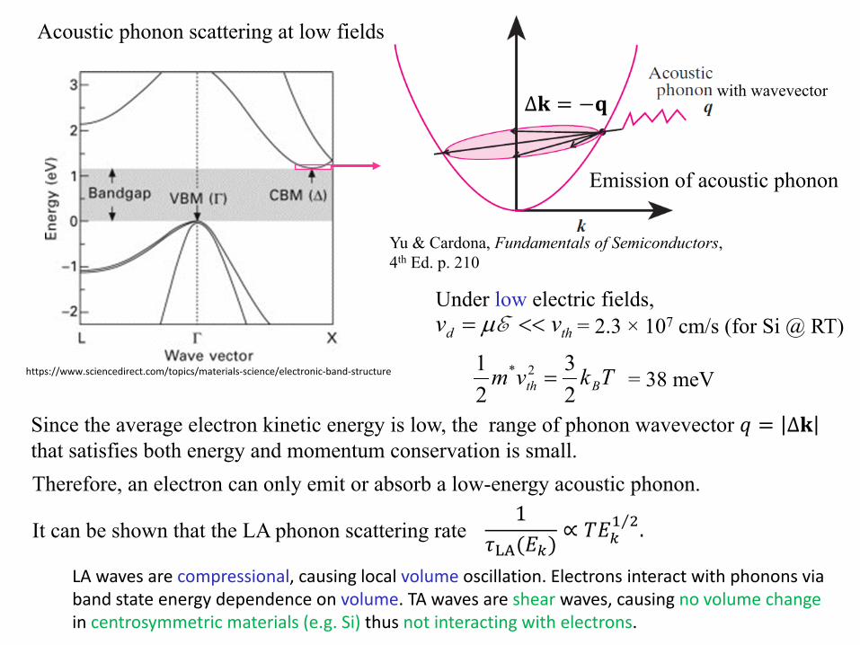
Acoustic phonon scattering at low fields
Under low electric fields,
Emission of acoustic phonon
thd vv <<= Eµ = 2.3 × 107 cm/s (for Si @ RT)
Therefore, an electron can only emit or absorb a low-energy acoustic phonon.
∆𝐤𝐤 = −𝐪𝐪with wavevector
Since the average electron kinetic energy is low, the range of phonon wavevector 𝑞𝑞 = ∆𝐤𝐤that satisfies both energy and momentum conservation is small.
1𝜏𝜏LA(𝑑𝑑𝑘𝑘)
∝ 𝑇𝑇𝑑𝑑𝑘𝑘⁄1 2.It can be shown that the LA phonon scattering rate
LA waves are compressional, causing local volume oscillation. Electrons interact with phonons via band state energy dependence on volume. TA waves are shear waves, causing no volume changein centrosymmetric materials (e.g. Si) thus not interacting with electrons.

1𝜏𝜏LA(𝑑𝑑𝑘𝑘)
∝ 𝑇𝑇𝑑𝑑𝑘𝑘⁄1 2LA phonon scattering rate ⇒ 𝜏𝜏LA(𝑑𝑑𝑘𝑘) ∝ 𝑇𝑇−1𝑑𝑑𝑘𝑘
⁄−1 2
⇒
15002000
3000
×2
×2
1𝜇𝜇
= �𝑖𝑖
1𝜇𝜇𝑖𝑖
For 𝑁𝑁𝐷𝐷 ~ 1014 cm−3, ion-scattering-limited mobility 𝜇𝜇i~ 107 ⁄cm2 (Vs) at 300 K.
Recall that if 𝜏𝜏(𝑑𝑑) ∝ 𝑑𝑑𝑛𝑛𝑇𝑇𝑚𝑚, because
For LA phonon scattering, n = −1/2 and m = −1.
𝜇𝜇LA ∝ 𝑇𝑇 ⁄−3 2 for LA phonon scattering.
Recall that𝜇𝜇i ∝ 𝑇𝑇 ⁄3 2 for ionized impurity scattering.
300
Obviously, at low doping the mobility is phonon limited.
Phonon-limited mobility is referred to as “intrinsic mobility”, e.g., 1500 ⁄cm2 (Vs)at 300 K for Si.

At low fields, thd vv <<= Eµ
Tkvm Bth 23
21 2* = = 38 meV
Under high fields, electrons gain energy faster from the field than they lose energy by scattering. ⇒Electrons & the lattice not in equilibrium. But electrons are in equilibrium with themselves, characterized by electron temperature 𝑇𝑇𝑒𝑒, higher than the lattice temperature. ⇒ Hot electrons.
vd
vsat
When the energy of hot electrons becomes comparable to that of optical phonons, energy is transferred to the lattice via optical phonons.
velocity saturation
For Si, vsat ~ 107 cm/s
High-field transport and hot carriers
vth = 2.3 × 107 cm/s (for Si @ RT)
Yu & Cardona, Fundamentals of Semiconductors, 4th Ed. p. 111
Curves: calculated. Circles: measured.
LA
TA
K
LA LA
TA
TA
TOTOTO
LO LO LO
E = hν = ħω= 62 meV @ 15 THz
New, high-rate scattering mechanism kicks in
104 V/cm = 1 mV/nmNotice this quite low value.
Think about FETs in analog circuits.

Charge Carriers in Semiconductors
Therefore, a full band does not conduct due to symmetry.Electron in band state moves at the group velocity.
Near a band minimum, the E-k dispersion (in most cases) can be written as:
For an intrinsic (perfect, pure) semiconductor at T = 0, valence band is full and conduction band empty. Thus no conduction.
Highlights
Generally in 3D, (𝑚𝑚𝑒𝑒∗)−1 is a tensor due to anisotropy. A single value
𝑚𝑚𝑒𝑒∗ is preferred for simplicity, which is averaged over all directions is a
way suitable for the purpose.
Full band does not conduct ⇒ concept of hole
missing electron
hole𝐯𝐯𝑒𝑒 𝐤𝐤𝑒𝑒 + �𝐤𝐤≠𝐤𝐤𝑒𝑒
𝐯𝐯(𝐤𝐤) = 0 𝐯𝐯𝑒𝑒 𝐤𝐤𝑒𝑒 = − �𝐤𝐤≠𝐤𝐤𝑒𝑒
𝐯𝐯(𝐤𝐤)⇒
The motion of all electrons can be described by that of hole:
�𝐤𝐤≠𝐤𝐤𝑒𝑒
𝐯𝐯(𝐤𝐤) = −𝐯𝐯𝑒𝑒 𝐤𝐤𝑒𝑒 = 𝐯𝐯(𝐤𝐤0 + (𝐤𝐤0 − 𝐤𝐤𝑒𝑒)) ≡ 𝐯𝐯 𝐤𝐤ℎ
𝑑𝑑0
as if only one electron at 𝐤𝐤ℎ is moving at 𝐯𝐯 𝐤𝐤ℎ .

Positive electric field ℰ drives entire band of electrons towards the negative k, thus the empty state moves to 𝑑𝑑𝑒𝑒 = 𝑑𝑑0 + ∆𝑑𝑑, where ∆𝑑𝑑 = −𝑞𝑞ℰ𝜏𝜏/ℏ.Corresponding momentum ℏ(𝑑𝑑𝑒𝑒 − 𝑑𝑑0) and group velocity 𝑣𝑣𝑒𝑒are negative.
�𝐤𝐤≠𝐤𝐤𝑒𝑒
𝐯𝐯(𝐤𝐤) = −𝐯𝐯𝑒𝑒 𝐤𝐤𝑒𝑒 = 𝐯𝐯(𝐤𝐤0 + (𝐤𝐤0 − 𝐤𝐤𝑒𝑒)) ≡ 𝐯𝐯 𝐤𝐤ℎas if only one electron at 𝐤𝐤ℎ is moving at 𝐯𝐯 𝐤𝐤ℎ .
𝑞𝑞𝑒𝑒𝐯𝐯 𝐤𝐤ℎ = −𝑞𝑞𝐯𝐯 𝐤𝐤ℎ = 𝑞𝑞 −𝐯𝐯 𝐤𝐤ℎ = 𝑞𝑞ℎ −𝐯𝐯 𝐤𝐤ℎ
missing electron
hole
𝑑𝑑0
Thus the electron at 𝐤𝐤ℎ moving at 𝐯𝐯 𝐤𝐤ℎ is represented by a hole at 𝐤𝐤ℎ, with charge +q, moving at −𝐯𝐯 𝐤𝐤ℎ ≡ 𝐯𝐯ℎ 𝐤𝐤ℎ .
𝑞𝑞ℎ = −𝑞𝑞𝑒𝑒 = +𝑞𝑞
𝐤𝐤ℎ = 𝐤𝐤0 + (𝐤𝐤0 − 𝐤𝐤𝑒𝑒) (𝐤𝐤ℎ = −𝐤𝐤𝑒𝑒 of 𝐤𝐤0 = 0)
𝐯𝐯ℎ 𝐤𝐤ℎ ≡ −𝐯𝐯 𝐤𝐤ℎ = +𝐯𝐯𝑒𝑒 𝐤𝐤𝑒𝑒
𝑑𝑑ℎ 𝐤𝐤ℎ = −𝑑𝑑𝑒𝑒 𝐤𝐤𝑒𝑒𝑚𝑚ℎ∗ = −𝑚𝑚𝑒𝑒
∗Subscripts e signify missing electron.
Semiclassical model: ℏ𝑑𝑑𝐤𝐤𝑑𝑑𝑑𝑑
= ℏ𝑑𝑑𝑑𝑑𝑑𝑑
(𝐤𝐤 − 𝐤𝐤0) = 𝐅𝐅
external force on electron
ℰ
∆𝑑𝑑
F does not include force on electrons due to lattice, taken care of by band picture (quantum). Newton’s laws apply to crystal momentum ℏ𝐤𝐤, not momentum. Thus semi-classical.
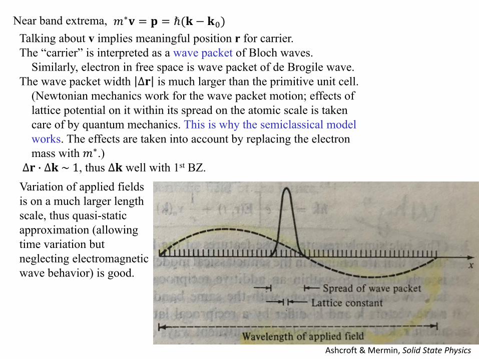
𝑚𝑚∗𝐯𝐯 = 𝐩𝐩 = ℏ(𝐤𝐤 − 𝐤𝐤0)Near band extrema, Talking about v implies meaningful position r for carrier. The “carrier” is interpreted as a wave packet of Bloch waves.
Similarly, electron in free space is wave packet of de Brogile wave. The wave packet width ∆𝐫𝐫 is much larger than the primitive unit cell.
(Newtonian mechanics work for the wave packet motion; effects of lattice potential on it within its spread on the atomic scale is taken care of by quantum mechanics. This is why the semiclassical model works. The effects are taken into account by replacing the electron mass with 𝑚𝑚∗.)
∆𝐫𝐫 � ∆𝐤𝐤 ~ 1, thus ∆𝐤𝐤 well with 1st BZ.
Ashcroft & Mermin, Solid State Physics
Variation of applied fields is on a much larger length scale, thus quasi-static approximation (allowing time variation but neglecting electromagnetic wave behavior) is good.

Generally in 3D, (𝑚𝑚∗)−1 is a tensor due to anisotropy. For simplicity, a single value 𝑚𝑚∗ is desirable. The 𝑚𝑚∗ here, averaged over all directions in a way suitable for describing “inertia” is called the conductivity effective mass.
In 𝑚𝑚∗𝐯𝐯 = 𝐩𝐩 = ℏ(𝐤𝐤 − 𝐤𝐤0), 𝑚𝑚∗ describes “inertia” of carrier.
The 𝑚𝑚∗ averaged in a way suitable for calculating DOS is density-of-states effective mass.
Electrons, as Fermions, follow F-D distribution 𝑓𝑓(𝑑𝑑).Due to the gap, 𝑓𝑓(𝑑𝑑) changes significantly upon rising T and introduction of carriers (unlike metals).
In non-degenerate semiconductors, carriers distributions, as tails of 𝑓𝑓(𝑑𝑑), are well approximated by Boltzmann distribution.
There are so few of them. The electron (hole) gas is pretty much like ideal gas.
𝑛𝑛 = �𝐸𝐸𝐶𝐶
∞𝐷𝐷(𝑑𝑑)𝑓𝑓(𝑑𝑑)𝑑𝑑𝑑𝑑 𝑝𝑝 = �
−∞
𝐸𝐸𝑉𝑉𝐷𝐷(𝑑𝑑)[1 − 𝑓𝑓 𝑑𝑑 ]𝑑𝑑𝑑𝑑Counting carriers:
Density of states 𝐷𝐷(𝑑𝑑) is calculated by counting states in a range dk, and then convert dk to dE according dispersion 𝑑𝑑(𝐤𝐤).
𝐷𝐷 𝑑𝑑 ∝ |𝑑𝑑 − 𝑑𝑑 𝑑𝑑0 |−1/2
𝐷𝐷 𝑑𝑑 ∝ |𝑑𝑑 − 𝑑𝑑 𝑑𝑑0 |1/23D:
1D:
For parabolic band dispersion,

Carriers can be introduced by doping. Good dopants are shallow impurities.
Shallow donors: group V dopants in group IV semiconductor, e.g., P in Si.Dopants are defects. P substitution of Si atoms perturbs the Si lattice. The extra e wanders in the long-range Coulomb potential of the P+ ion.
Shallow defects are characterized by long-range potentials.This long-range potential determines the energy levels of the bound e.
A deep defect may have a shallow bound e energy level, but is characterized by its short-range potential.
The H atom model approximates shallow impurities, yielding right order of magnitude of the bound level (ionization energy).
While ionization energies same order of magnitude but > 𝑑𝑑𝐵𝐵𝑇𝑇, essentially all donors are ionized, i.e., 𝑛𝑛 = 𝑁𝑁𝐷𝐷+ = 𝑁𝑁𝐷𝐷 if 𝑁𝑁𝐷𝐷 ≪ 𝑁𝑁𝐶𝐶.
The semiconductor is said to be non-degenerate in this case.At very high T, intrinsic carriers overwhelm those introduced by doping. At very low T, carriers are frozen out (from conduction band to bound state).(See slides 35-37.)

Charge transportSemiclassical model: ℏ
𝑑𝑑𝐤𝐤𝑑𝑑𝑑𝑑
= ℏ𝑑𝑑𝑑𝑑𝑑𝑑
(𝐤𝐤 − 𝐤𝐤0) = 𝐅𝐅external force on electron
Interactions between electrons and perfect (periodic) lattice already accounted for by band theory. No defects, no scattering.
Field drives carriers out of equilibrium.Scattering relaxes them back to equilibrium.
In relaxation time 𝜏𝜏𝐤𝐤 = 𝜏𝜏(𝑑𝑑𝐤𝐤), a scattering mechanism (e.g. ionized impurity, phonon) undoes momentum gained from the field by electron in band state (𝐤𝐤,𝑑𝑑𝐤𝐤).
The two mechanisms balance at a steady state. The steady state carrier distribution 𝑓𝑓𝐤𝐤 = 𝑓𝑓𝐤𝐤
(0) + 𝑔𝑔𝐤𝐤(𝓔𝓔).The extra part 𝑔𝑔𝐤𝐤(𝓔𝓔) in addition to the equilibrium distribution 𝑓𝑓𝐤𝐤
(0) is the result of the balancing action between the field and scattering (relaxation).
Therefore, 𝑔𝑔𝐤𝐤 is calculated as such.Only the extra part 𝑔𝑔𝐤𝐤(𝓔𝓔) contributes to net current.
Therefore, net current density J is calculated as such, which is, of course, ∝ 𝓔𝓔.⇒ Ohm’s law.
The conductivity contributed by all carriers at all energies E is

𝜎𝜎 =𝑞𝑞2𝑛𝑛 𝜏𝜏𝑚𝑚∗We’d love a single value, the average scattering time 𝜏𝜏 , so that
Therefore, the average scattering time 𝜏𝜏 is: 𝜏𝜏 =𝑚𝑚∗
𝑞𝑞2𝜎𝜎𝑛𝑛
Insert Eq. (5.25)
𝑛𝑛 = �𝐷𝐷 𝑑𝑑 𝑓𝑓 𝑑𝑑 𝑑𝑑𝑑𝑑
𝐷𝐷 𝑑𝑑 ∝ 𝑑𝑑
Once we know 𝜏𝜏𝑖𝑖(𝑑𝑑) for a particular scattering mechanism i, we can find 𝜏𝜏𝑖𝑖 and thus its signature dependence on T. Since𝜇𝜇𝑖𝑖 ∝ 𝜏𝜏𝑖𝑖 , 𝜇𝜇𝑖𝑖has the same dependence.
Thus
If 𝜏𝜏(𝑑𝑑) ∝ 𝑑𝑑𝑛𝑛𝑇𝑇𝑚𝑚,
1𝜏𝜏
= �𝑖𝑖
1𝜏𝜏𝑖𝑖
1𝜇𝜇
= �𝑖𝑖
1𝜇𝜇𝑖𝑖
The overall transport figures and
From the dependence of on T (and carrier density), we can estimate the contributions of each scattering mechanism.

And, 𝜇𝜇i ∝ 𝜏𝜏i ∝ 𝑛𝑛𝑒𝑒− ⁄2 3
For charged impurity scattering in non-degenerate semiconductors with no other impurities other than ionized dopants (𝑁𝑁i = 𝑁𝑁𝐷𝐷 = 𝑛𝑛𝑒𝑒),
Therefore, n = 3/2 and m = 0.
1𝜏𝜏i(𝑑𝑑𝑘𝑘)
∝ 𝑛𝑛𝑒𝑒𝑑𝑑𝑘𝑘− ⁄3 2.
⇒
Electron concentration
𝜇𝜇i ∝ 𝑇𝑇 ⁄3 2 for ionized impurity scattering.
Under low fields, carriers only interact with low-energy acoustic phonons.(only with low-energy LA phonons in centrosymmetric materials, e.g., Si.)
1𝜏𝜏LA(𝑑𝑑𝑘𝑘)
∝ 𝑇𝑇𝑑𝑑𝑘𝑘⁄1 2LA phonon scattering rate ⇒ 𝜏𝜏LA(𝑑𝑑𝑘𝑘) ∝ 𝑇𝑇−1𝑑𝑑𝑘𝑘
⁄−1 2
⇒Therefore, n = −1/2 and m = −1. 𝜇𝜇LA ∝ 𝑇𝑇 ⁄−3 2 for LA phonon scattering.
LA phonon scattering and ionized impurity scattering are the two major scattering mechanisms in Si.
For 𝑁𝑁i = 𝑁𝑁𝐷𝐷 < ~ 1014 cm−3, scattering in Si is phonon-limited . Phonon-limited mobility is referred to as “intrinsic mobility”. The electron mobility of 1500 ⁄cm2 (Vs) at 300 K for Sioften quoted by textbooks is such “intrinsic mobility”.

Under high fields, carriers gain energy faster than they lose to scattering. ⇒Electrons & the lattice not in equilibrium. In equilibrium with themselves, electrons are hotter than the lattice. ⇒Hot electrons.
When the energy of hot electrons becomes comparable to that of optical phonons, energy is transferred to the lattice via optical phonons.
velocity saturationNew, high-rate scattering mechanism kicks in
vd
vsatFor Si, vsat ~ 107 cm/s
104 V/cm = 1 mV/nm