A flexible p-CuO/n-MoS2 heterojunction photodetector with enhanced … · · 2017-01-272...
7
This journal is © The Royal Society of Chemistry 2017 Mater. Horiz. Cite this: DOI: 10.1039/c6mh00568c A flexible p-CuO/n-MoS 2 heterojunction photodetector with enhanced photoresponse by the piezo-phototronic effect† Ke Zhang,‡ a Mingzeng Peng,‡ a Wei Wu, a Junmeng Guo, a Guoyun Gao, a Yudong Liu, a Jinzong Kou, a Rongmei Wen, a Ying Lei, a Aifang Yu, a Yang Zhang, a Junyi Zhai* a and Zhong Lin Wang* ab Flexible functional devices based on two dimensional (2D) materials are extremely suitable for malleable, portable and sustainable applica- tions, such as health monitoring, electronic skin and optoelectronics. In this work, we developed a flexible photodetector based on a p-CuO/n-MoS 2 heterojunction with an enhancement in photocurrent and detection sensitivity. Because of the non-centrosymmetric struc- ture in monolayer MoS 2 , the piezo-potential induced by applied strain adjusts the band structure at the heterojunction interface and broadens the depletion region based on the piezo-phototronic effect. The border depletion can be discreetly used to improve the photo- generated carrier separation and transport to enhance photo- response performance. When illuminated by a 532 nm laser, the photocurrent of the heterojunction can be enhanced 27 times under a tensile strain of 0.65% compared to strain free conditions and the detection sensitivity can reach up to 3.27 Â 10 8 Jones. As a result, our research provides a new strategy for novel design and performance optimization of 2D material heterostructures in the application of optoelectronics. Introduction Transition metal dichalcogenides (TMDCs) have recently emerged as a new class of semiconductor materials of electronics and optoelectronics. 1,2 Molybdenum disulfide (MoS 2 ), the representa- tive of TMDCs, not only has a 1.8 eV direct band gap for the monolayer, which is superior to that of graphene (zero gap), but also has other advantages such as good stability and brilliant optoelectronic properties. 2–4 However, most photodetectors, 5,6 phototransistors, 7 solar cells 8,9 and other optoelectronic devices with excellent performance based on monolayer MoS 2 are often fabricated on hard substrates (silicon wafer, sapphire, etc.). 2D materials, owing to their outstanding ductility and high mechanical strength, 10 are well adapted for flexible optoelectronic devices in new application fields, such as biomedical diagnosis, personal health monitoring and wearable communication. 11–13 However, it is challenging to achieve a better performance on polymer-based flexible substrates due to inevitable substrate strain, the limitation of transferring methods and complex fabrication. Among them, for flexible optoelectronics, strain from a flexible substrate has a large influence on the device performance, due to the piezoresistive effect, stress concentration and stress softening. Although there were a few reports 14,15 of TMD based flexible devices in the last several years, they avoided or reduced the impact of strain as far as possible. Our study aims at applying the inevitable substrate strain to improve the performance of photodetectors based on the strong piezo- electric effect in monolayer MoS 2 . a Beijing Institute of Nanoenergy and Nanosystems, Chinese Academy of Science, National Center for Nanoscience and Technology (NCNST), Beijing 100083, P. R. China. E-mail: [email protected], [email protected] b School of Materials Science and Engineering, Georgia Institute of Technology, Atlanta, Georgia 30332-0245, USA † Electronic supplementary information (ESI) available. See DOI: 10.1039/ c6mh00568c ‡ These authors contributed equally to this work. Received 8th December 2016, Accepted 13th January 2017 DOI: 10.1039/c6mh00568c rsc.li/materials-horizons Conceptual insights Transition metal dichalcogenide (TMD) material based optoelectronic devices have been developed rapidly due to their excellent visible light response and ultra-fast photovoltaic conversion. We demonstrate that applied strain can further dramatically tune the optoelectronic properties in TMD p–n junctions owing to piezo-phototronics, while most of the previous studies have avoided or reduced the impact of strain dependent properties. The largest piezoelectric effect in monolayer MoS 2 is in-plane and occurs along the Mo–S bond orientation, which can easily be identified by the triangle shape of CVD-grown MoS 2 . When strain is applied to MoS 2 along the Mo–S bond direction, piezo-charge will be induced and control the carrier generation, transport, separation and/or recombination at the interface of p-CuO/n-MoS 2 , improving the performance of optoelectronic devices. As a result, both the photo- induced current and sensitivity of the pn junction based photodetector are largely enhanced. This method provides a new strategy to improve the optoelectronic properties in TMD based pn junctions by applying strain. Materials Horizons COMMUNICATION Published on 13 January 2017. Downloaded by Georgia Institute of Technology on 27/01/2017 21:20:51. View Article Online View Journal
Transcript of A flexible p-CuO/n-MoS2 heterojunction photodetector with enhanced … · · 2017-01-272...

This journal is©The Royal Society of Chemistry 2017 Mater. Horiz.
Cite this:DOI: 10.1039/c6mh00568c
A flexible p-CuO/n-MoS2 heterojunctionphotodetector with enhanced photoresponse bythe piezo-phototronic effect†
Ke Zhang,‡a Mingzeng Peng,‡a Wei Wu,a Junmeng Guo,a Guoyun Gao,a
Yudong Liu,a Jinzong Kou,a Rongmei Wen,a Ying Lei,a Aifang Yu,a Yang Zhang,a
Junyi Zhai*a and Zhong Lin Wang*ab
Flexible functional devices based on two dimensional (2D) materials
are extremely suitable for malleable, portable and sustainable applica-
tions, such as health monitoring, electronic skin and optoelectronics.
In this work, we developed a flexible photodetector based on a
p-CuO/n-MoS2 heterojunction with an enhancement in photocurrent
and detection sensitivity. Because of the non-centrosymmetric struc-
ture in monolayer MoS2, the piezo-potential induced by applied
strain adjusts the band structure at the heterojunction interface and
broadens the depletion region based on the piezo-phototronic effect.
The border depletion can be discreetly used to improve the photo-
generated carrier separation and transport to enhance photo-
response performance. When illuminated by a 532 nm laser, the
photocurrent of the heterojunction can be enhanced 27 times
under a tensile strain of 0.65% compared to strain free conditions
and the detection sensitivity can reach up to 3.27 � 108 Jones.
As a result, our research provides a new strategy for novel design
and performance optimization of 2D material heterostructures in
the application of optoelectronics.
Introduction
Transition metal dichalcogenides (TMDCs) have recently emergedas a new class of semiconductor materials of electronics andoptoelectronics.1,2 Molybdenum disulfide (MoS2), the representa-tive of TMDCs, not only has a 1.8 eV direct band gap for themonolayer, which is superior to that of graphene (zero gap), butalso has other advantages such as good stability and brilliantoptoelectronic properties.2–4 However, most photodetectors,5,6
phototransistors,7 solar cells8,9 and other optoelectronic deviceswith excellent performance based on monolayer MoS2 are oftenfabricated on hard substrates (silicon wafer, sapphire, etc.).2D materials, owing to their outstanding ductility and highmechanical strength,10 are well adapted for flexible optoelectronicdevices in new application fields, such as biomedical diagnosis,personal health monitoring and wearable communication.11–13
However, it is challenging to achieve a better performance onpolymer-based flexible substrates due to inevitable substratestrain, the limitation of transferring methods and complexfabrication. Among them, for flexible optoelectronics, strainfrom a flexible substrate has a large influence on the deviceperformance, due to the piezoresistive effect, stress concentrationand stress softening. Although there were a few reports14,15 ofTMD based flexible devices in the last several years, they avoidedor reduced the impact of strain as far as possible. Our studyaims at applying the inevitable substrate strain to improve theperformance of photodetectors based on the strong piezo-electric effect in monolayer MoS2.
a Beijing Institute of Nanoenergy and Nanosystems, Chinese Academy of Science,
National Center for Nanoscience and Technology (NCNST), Beijing 100083,
P. R. China. E-mail: [email protected], [email protected] School of Materials Science and Engineering, Georgia Institute of Technology,
Atlanta, Georgia 30332-0245, USA
† Electronic supplementary information (ESI) available. See DOI: 10.1039/c6mh00568c‡ These authors contributed equally to this work.
Received 8th December 2016,Accepted 13th January 2017
DOI: 10.1039/c6mh00568c
rsc.li/materials-horizons
Conceptual insightsTransition metal dichalcogenide (TMD) material based optoelectronicdevices have been developed rapidly due to their excellent visible lightresponse and ultra-fast photovoltaic conversion. We demonstrate thatapplied strain can further dramatically tune the optoelectronic propertiesin TMD p–n junctions owing to piezo-phototronics, while most of theprevious studies have avoided or reduced the impact of strain dependentproperties. The largest piezoelectric effect in monolayer MoS2 is in-planeand occurs along the Mo–S bond orientation, which can easily beidentified by the triangle shape of CVD-grown MoS2. When strain isapplied to MoS2 along the Mo–S bond direction, piezo-charge will beinduced and control the carrier generation, transport, separation and/orrecombination at the interface of p-CuO/n-MoS2, improving theperformance of optoelectronic devices. As a result, both the photo-induced current and sensitivity of the pn junction based photodetectorare largely enhanced. This method provides a new strategy to improve theoptoelectronic properties in TMD based pn junctions by applying strain.
MaterialsHorizons
COMMUNICATION
Publ
ishe
d on
13
Janu
ary
2017
. Dow
nloa
ded
by G
eorg
ia I
nstit
ute
of T
echn
olog
y on
27/
01/2
017
21:2
0:51
.
View Article OnlineView Journal
Mater. Horiz. This journal is©The Royal Society of Chemistry 2017
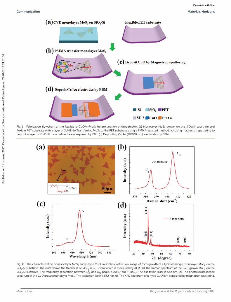
Fig. 1 Fabrication flowchart of the flexible p-CuO/n-MoS2 heterojunction photodetector. (a) Monolayer MoS2 grown on the SiO2/Si substrate andflexible PET substrate with a layer of SU-8. (b) Transferring MoS2 to the PET substrate using a PMMA-assisted method. (c) Using magnetron sputtering todeposit a layer of CuO film on defined areas exposed by EBL. (d) Depositing Cr/Au (10/100 nm) electrodes by EBM.
Fig. 2 The characterization of monolayer MoS2 and p-type CuO. (a) Optical reflection image of CVD growth of a typical triangle monolayer MoS2 on theSiO2/Si substrate. The inset shows the thickness of MoS2 is E0.7 nm which is measured by AFM. (b) The Raman spectrum of the CVD grown MoS2 on theSiO2/Si substrate. The frequency separation between E1
2g and A1g peaks is 20.07 cm�1 MoS2. The excitation laser is 532 nm. (c) The photoluminescencespectrum of the CVD grown monolayer MoS2. The excitation laser is 532 nm. (d) The XRD spectrum of p-type CuO film deposited by magnetron sputtering.
Communication Materials Horizons
Publ
ishe
d on
13
Janu
ary
2017
. Dow
nloa
ded
by G
eorg
ia I
nstit
ute
of T
echn
olog
y on
27/
01/2
017
21:2
0:51
. View Article Online

This journal is©The Royal Society of Chemistry 2017 Mater. Horiz.
Recently, a piezoelectric effect in MoS2 with an odd number ofatomic layers was reported which could be used to modulate theheight of the schottky barrier in metal-semiconductor contactsand/or power nano-devices owing to its non-centrosymmetricstructure13,16 Moreover, it is easy to identify the Mo–S bondorientation (direction with a strongest piezoelectric effect) fromthe triangular single-layer CVD grown MoS2.17,18 Meanwhile, thepiezo-phototronic effect is to use the piezopotential to control thecarrier generation, transport, separation and/or recombinationfor improving the performance of optoelectronic devices, such asphotodetectors, solar cells, LEDs and pressure-sensitive photo-luminescence imaging.19–23 Although the piezo-phototroniceffect has been well studied in wurtzite ZnO or GaN nanowirebased LEDs, solar cells and photodetectors, there is still a lack ofresearch on how piezopotential tunes the photoelectric proper-ties in a monolayer 2D material based heterostructure.24,25
In this study, we developed a flexible p-CuO/n-MoS2 hetero-junction photodetector to obtain high optoelectronic perfor-mance by the piezo-phototronic effect. High quality triangularmonolayer n-type MoS2 grown by chemical vapor deposition(CVD) was used to form a p–n heterojunction with a p-type CuOfilm deposited by magnetron sputter deposition. Under theexternal stimuli, the piezopotential induced by piezoelectriccharges at the side of the monolayer MoS2 adjusted the bandstructure at the interface of the heterojunction and separated
the photogenerated electron–hole pairs more effectively to increasethe photocurrent. In addition, the structure of the p–n junctioncan also reduce the screening effect from a lot of free electrons inn-type materials and depress the dark current in order to get largerphotoresponsivity and higher detection sensitivity. Our flexiblephotodetector based on p-CuO/n-MoS2 gave an ultra-low darkcurrent of 0.039 nA and a detection sensitivity of 3.27 � 108 Jones.The results demonstrate that the piezo-phototronic effect haspotential for improving the performance of electronics andoptoelectronics based on 2D materials and related heterostruc-tures, especially for flexible sensing applications.
Results and discussion
The fabrication process of the flexible CuO–MoS2 hetero-junction device is illustrated in Fig. 1. MoS2 monolayers werefirstly grown on silicon wafers with a 300 nm thick silica layer(SiO2/Si) by chemical vapor deposition (CVD), as described inprevious studies.18,26 Secondly, an SU-8 photoresist was spin-coated on a PET substrate to get a relatively flat and smoothsurface. After spin-coating, the PET substrate was baked at135 1C for two hours. Thirdly, the monolayer CVD-grown MoS2
was transferred to the PET substrate by using polymethyl-methacrylane (PMMA) as shown in Fig. 1b.27,28 Fourthly, a
Fig. 3 (a) Schematic diagram of the flexible photodetector based on the p-CuO/n-MoS2 heterojunction. (b) I–V curve of the p-CuO/n-MoS2
heterojunction in the dark and in a strain free state. The inset is the optical image of the device. (c) I–V curves of the heterojunction in the dark withincreasing tensile strain. (d) I–V curves measured at 0.65% tensile strain and different illumination light powers. All curves were measured at roomtemperature and in the air. A 532 nm laser was used to excite the photocurrent.
Materials Horizons Communication
Publ
ishe
d on
13
Janu
ary
2017
. Dow
nloa
ded
by G
eorg
ia I
nstit
ute
of T
echn
olog
y on
27/
01/2
017
21:2
0:51
. View Article Online

Mater. Horiz. This journal is©The Royal Society of Chemistry 2017
PMMA electron beam resist was spun on the PET substrate anda specific area was exposed by electron beam lithography.Fifthly, a 150 nm thick p-type CuO film was deposited bymagnetron sputtering to form a p–n junction with MoS2. Finally,Cr/Au (10 nm/100 nm) electrodes were deposited on both sides ofthe p-CuO/n-MoS2 heterojunction by electron beam lithography(EBL) and electron beam evaporation deposition (EBM) (Fig. 1cand d). In detail, the polarity orientation (C axis) of the CVD-grownMoS2 from the S to Mo atom with a strongest piezoelectric effectwas indicated by the red arrow as shown in Fig. 1e. In order toinvestigate the performance modulation of the piezoelectric effect,both the rectangle p-type CuO film and Cr/Au electrodes weredeposited perpendicular to the C axis of MoS2.
Fig. 2a shows the surface morphology of the CVD growntriangle MoS2 on the SiO2/Si substrate using an optical micro-scope. The typical side length ranges from 40 to 70 mm. Besides,the thickness of the MoS2 flakes is around 0.7 nm, measured byatomic force microscopy (AFM), which approaches the theoreticalthickness of monolayer MoS2.29 Raman and photoluminescence(PL) spectra of the CVD-grown monolayer MoS2 flakes are pre-sented in Fig. 2b and c, respectively. The energy difference betweenits A1g (405.02 cm�1) and E1
2g (384.95 cm�1) Raman modes is20.07 cm�1, confirming that the MoS2 flakes are monolayers.30,31
The PL spectrum consists of two peaks at 670 nm (1.85 eV) and620 nm (2.00 eV), corresponding to the A and B direct gap opticaltransition.32 P-type CuO film was fabricated by a standard
magnetron sputter deposition using a high purity Cu target andAr/O2 (1 : 4) sputtering gases at room temperature. It has excellentquality further proved by the XRD spectrum (Fig. 2d).33,34
The structure of the flexible p-CuO/n-MoS2 heterojunctionphotodetector is demonstrated in Fig. 3a. We used a 532 nmlaser (facula diameter is about 3 mm), to illuminate the side ofMoS2 and avoid the photoresponse influence from the p-CuOlayer. A high precision manual translation table was used tobend the PET substrate. By this means, well controlled strain canbe applied to the monolayer MoS2, as shown in Fig. S1 (ESI†).Moreover, we examined the photoresponse of the pure p-CuOfilm in different tensile strain states and at various optical powerdensities (Fig. S2a and S2b, ESI†). The results indicate that thephotoresponse of CuO in the scope of illumination power is verysmall and can be omitted comparing to the performance of thep–n heterojunction device. The photoresponse of pure mono-layer MoS2 is also studied and the device just performs thepiezoresistive effect (Fig. S2c and S2d, ESI†). Next, the I–Vcharacteristics of the p-CuO/n-MoS2 heterojunction were inves-tigated with various illumination power densities and strains.Fig. 3b shows good rectification characteristics of the p-CuO/n-MoS2 heterojunction under dark and strain free conditions. Ithad an ultra-low dark current of 0.039 nA even under 10 Vforward bias, which was advantageous for high performanceoptical sensing. The relationship of the photogenerated currentwith different strains in the dark is presented in Fig. 3c.
Fig. 4 The strain dependence of the (a) photocurrent, (b) DI/Idark, (c) R/R0 and (d) detectivity (D*) at different power densities at a bias of 10 V.
Communication Materials Horizons
Publ
ishe
d on
13
Janu
ary
2017
. Dow
nloa
ded
by G
eorg
ia I
nstit
ute
of T
echn
olog
y on
27/
01/2
017
21:2
0:51
. View Article Online

This journal is©The Royal Society of Chemistry 2017 Mater. Horiz.
The dark current under 10 V bias increases from 0.039 nA to0.12 nA with increasing tensile strain from 0% to 0.65%. This ismainly attributed to the piezotronic effect of single layer MoS2
(positive piezopotential induced by tensile strain tunes thebandgap at the heterojunction interface of CuO and MoS2). Inorder to further investigate the influence of the piezo-phototroniceffect on the p-CuO/n-MoS2 heterojunction performance, wetested the I–V characteristic with increasing illumination powerdensity from dark to 1656 mW cm�2 and tensile strain from 0% to0.65%. The photocurrent is always enhanced with the increasingof either the luminous power or tensile strain. The photocurrentof the p–n heterojunction device can reach to the maximumvalue of 108 nA under 1656 mW cm�2 illumination and 0.65%tensile strain, which is about a 2770 times improvement incurrent output compared to its dark current in a strain free state.Meanwhile, the time-dependent photoresponse of the device toperiodical on/off illumination under different tensile strains isshown in Fig. S3 (ESI†). The device has excellent stability undervarious strains over a long time period.
According to the I–V characteristics of the p-CuO/n-MoS2 hetero-junction photodetector, we evaluated the photocurrent (Iph), photo-sensitivity (DI/Idark), relative changes in photoresponsivity (R/R0), anddetectivity (D*) under different illumination intensities (0 mW cm�2
(dark), 2.66 mW cm�2, 135.92 mW cm�2, 653.50 mW cm�2,1656.05 mW cm�2) and tensile strains (0%, 0.18%, 0.31%, 0.65%),
as summarized in Fig. 4. The relationship of photocurrent Iph
with different tensile strains under various power densitiesis shown in Fig. 4a. Under the 532 nm laser illumination, thephotocurrent increases with the increasing of strain due to thepiezo-phototronic effect. When the illumination power is fixedat 1656.05 mW cm�2, the photocurrent Iph is enhanced 27 timesunder a strain of 0.65% compared with strain-free conditions.To demonstrate its photoresponse mechanism clearly,the photosensitivity is calculated using the formula DI/Idark =(Ilight� Idark)/Idark, where the Ilight and Idark are the output currentwith and without illumination under a certain external strain,respectively. Meanwhile, the relative change in responsivity isdefined as R/R0 (R0 is the corresponding R under strain-freeconditions) for different power densities. It can be seen thatthe relationships of DI/Idark and R/R0 with tensile strain have asimilar manner as photocurrent Iph under different illuminationpowers in Fig. 4b and c. The maximum values of DI/Idark and R/R0
are 873 and 2680% respectively, achieved at the highest tensilestrain of 0.65% and light power of 1656.05 mW cm�2, owing tothe piezo-phototronic effect on modulating energy and thestructure at the interface of CuO/MoS2. Moreover, we show thephotoresponsivity of our photodetector in Fig. S4 (ESI†), whichalso increases with the increasing of strain due to the piezo-phototronic effect. The detectivity under different strains iscalculated using formula the D* = R/(2eIdark/S)0.5, where e is the
Fig. 5 (a) Band diagram of the p-CuO/n-MoS2 heterojunction in the equilibrium state with forward bias. DEc = 0.13 eV, DEv = 0.68 eV. (b) Band diagramwith forward-bias voltage in a strain free state (black line) and tensile strain state (purple line). When tensile strain is applied, the induced positivepiezoelectric polarization charges at the interface will cause a decline for the band edge (purple line) and increase the width of the depletion zone. Forthe color gradient, red represents positive potential and blue represents negative potential.
Materials Horizons Communication
Publ
ishe
d on
13
Janu
ary
2017
. Dow
nloa
ded
by G
eorg
ia I
nstit
ute
of T
echn
olog
y on
27/
01/2
017
21:2
0:51
. View Article Online

Mater. Horiz. This journal is©The Royal Society of Chemistry 2017
quantity of electric charge, Idark is dark current and S isthe effective surface area of the CuO/MoS2 heterojunctionphotodetector. We found that D* reaches the highest value of3.27 � 108 Jones under the highest strain of 0.65% and lowerlight power of 2.66 mW cm�2 in Fig. 4d.
In order to elucidate the intrinsic mechanism of piezo-phototronics for modulating the photoresponse performanceof the p-CuO/n-MoS2 heterojunction, its band structures ofthe heterojunction with/without tensile strain have been com-pared. Fig. 5a shows its band diagrams under strain-free andforward bias conditions. The electron affinity and band gap ofp-CuO are 4.07 eV and 1.35 eV, respectively35 while the mono-layer MoS2 has 4.2 eV electron affinity and 1.8 eV direct bandgap.36 Therefore, a conduction band offset DEc = 0.13 eV and avalence band offset DEv = 0.68 eV present at local heterostruc-ture interface. The electrons and holes flow towards CuO andMoS2 respectively because of the joint action of built-in electricfield and external forward bias. Under the laser irradiation of532 nm (2.33 eV), the photo-generated electron–hole pairs areseparated by a built-in field, producing external photocurrent.When tensile strain is applied to the flexible device, monolayerMoS2 generates the mechanical deformation and producespositive piezoelectric charges at the heterostructure interfacedue to the piezotronic effect. As a result, the positive piezo-potential induced by polarization charges enhances the con-duction band and valence band energy level bending of MoS2
near the interface and the depletion zone is broadened at thesame time. At the interface of CuO/MoS2, both stronger electricfield and the expanded depletion zone provide an extra drivingforce to separate photo-generated electrons and holes moreefficiently. Meanwhile, it also reduces the recombination ofphotogenerated electron–hole pairs, accelerates the transporta-tion of carriers and increases photocurrent. Therefore, under theforward bias, the photocurrent increases a lot mainly becauseof the piezo-phototronic effect (Fig. 5b). Of course, the piezo-resistive effect can also cause an increase of photocurrent, but it isconsidered as the ‘‘volume effect’’ and has an equivalent change inthe device performance under either dark or illumination condi-tions, as shown in Fig. S2d (ESI†). However, our experimentalresults manifest that the performance of the photodetector hasmore enhancement by applying tensile strain in illumination thanthat in the dark. In summary, the piezo-phototronic effect playsa major role in the photoresponse enhancement of the p-CuO/n-MoS2 photodetector.
Conclusions
In summary, we successfully fabricated a flexible and high-performance p-CuO/n-MoS2 heterojunction based photo-detector. We take advantage of the unique characteristics inCVD-grown monolayer MoS2, such as a strong piezoelectric effectand simple determination of polarity direction, to optimize theoptoelectronic performance of flexible detectors by appliedstrain. Based on the piezo-phototronic effect, the piezopotentialinduced by monolayer MoS2 under strain conditions has
dramatically adjusted the band structure in the interfaceof the monolayer MoS2-based heterojunction and separatedphotogenerated electron–hole pairs more effectively to increasethe device photocurrent. Here, the flexible p-CuO/n-MoS2
photodetector under 0.65% tensile strain has up to 27 timesimprovement in responsivity compared to strain-free condi-tions with a detection sensitivity of 3.27 � 108 Jones in low lightillumination. Due to the ultra-flexibility and high mechanicalstrength of 2D materials, TMDCs (MoS2, WSe2, MoTe2, etc.)with the piezoelectric effect will be more competitive fornanoelectronic devices for applications in flexible sensors andultrathin optoelectronics.
MethodsGrowth procedure and transfer of MoS2
Monolayer MoS2 was grown on 300 nm thick SiO2/Si sub-strates by chemical vapor deposition. A quartz boat containing15 mg MoO3 powder (Z99.5%, Sigma Aldrich), which served asa precursor, was positioned in the center of a furnace and the Sisubstrate was placed face down in the boat above the precursor.270 mg sulfur (Z99.9%, Aladdin) was located outside of thefurnace, warmed up by heating tape. The furnace temperaturewas increased up to 750 1C at a rate of 15 1C min�1 and heldconstant for 30 minutes at this point, and then cooled downnaturally. When the furnace temperature reached 650 1C, theheating tape started working. The growth was carried on underatmospheric pressure with 10 sccm argon flow.
During the transfer process, a thin layer of PMMA (495 K,A11, MicroChem) was spun coated firstly on the CVD grownMoS2, and then baked for 3 minutes at 150 1C. Next, the samplecoated by PMMA was floated on 30% HF solution to etch SiO2.Finally, the detached film was cleaned in deionized waterseveral times and transferred to the target substrate.
Author contribution
The manuscript was written through contributions of allauthors. All authors have given approval to the final version ofthe manuscript. K. Z., J. Y. Z and Z. L. W conceived the idea. K. Z.and J. M. G. prepared the materials. K. Z., W. W., and G. Y. G.fabricated the devices. K. Z., M. Z. P. and Y. D. L. conducted theelectrical test. J. Z. K, R. M. W., Y. L., A. F. Y., and Y. Z performedthe material characterization. K. Z. and M. Z. P. analyzed thedata and wrote the manuscript instructed by J. Y. Z. and Z. L. W.with input from all the authors.
Acknowledgements
This work was supported by NSFC 51472056 and 51402064, the‘‘thousands talents’’ program for pioneer researcher and hisinnovation team, China, the Recruitment Program of GlobalYouth Experts, China, Youth Innovation Promotion Associationof Chinese Academy of Sciences (2015387) and The National KeyResearch and Development Program of China (2016YFA0202703).
Communication Materials Horizons
Publ
ishe
d on
13
Janu
ary
2017
. Dow
nloa
ded
by G
eorg
ia I
nstit
ute
of T
echn
olog
y on
27/
01/2
017
21:2
0:51
. View Article Online

This journal is©The Royal Society of Chemistry 2017 Mater. Horiz.
Notes and references
1 S. Das, J. A. Robinson, M. Dubey, H. Terrones andM. Terrones, Annu. Rev. Mater. Res., 2015, 45, 1–27.
2 Q. H. Wang, K. Kalantar-Zadeh, A. Kis, J. N. Coleman andM. S. Strano, Nat. Nanotechnol., 2012, 7, 699–712.
3 K. F. Mak, C. Lee, J. Hone, J. Shan and T. F. Heinz, Phy. Rev.Lett., 2010, 105, 136805.
4 A. K. Geim and K. S. Novoselov, Nat. Mater., 2007, 6,183–191.
5 C. Chen, H. Qiao, S. Lin, C. Man Luk, Y. Liu, Z. Xu, J. Song,Y. Xue, D. Li, J. Yuan, W. Yu, C. Pan, S. Ping Lau and Q. Bao,Sci. rep., 2015, 5, 11830.
6 O. Lopez-Sanchez, D. Lembke, M. Kayci, A. Radenovic andA. Kis, Nat Nanotechnol., 2013, 8, 497–501.
7 W. Choi, M. Y. Cho, A. Konar, J. H. Lee, G.-B. Cha,S. C. Hong, S. Kim, J. Kim, D. Jena, J. Joo and S. Kim, Adv.Mater., 2012, 24, 5832–5836.
8 S. Lin, X. Li, P. Wang, Z. Xu, S. Zhang, H. Zhong, Z. Wu,W. Xu and H. Chen, Sci. Rep., 2015, 5, 15103.
9 M.-L. Tsai, S.-H. Su, J.-K. Chang, D.-S. Tsai, C.-H. Chen,C.-I. Wu, L.-J. Li, L.-J. Chen and J.-H. He, ACS Nano, 2014, 8,8317–8322.
10 S. Bertolazzi, J. Brivio and A. Kis, ACS Nano, 2011, 5,9703–9709.
11 D. Ruh, P. Reith, S. Sherman, M. Theodor, J. Ruhhammer,A. Seifert and H. Zappe, Adv. Mater., 2014, 26, 1706–1710.
12 D. Akinwande, N. Petrone and J. Hone, Nat. Commun., 2014,5, 5678.
13 W. Wu, L. Wang, Y. Li, F. Zhang, L. Lin, S. Niu, D. Chenet,X. Zhang, Y. Hao, T. F. Heinz, J. Hone and Z. L. Wang,Nature, 2014, 514, 470–474.
14 M.-Y. Tsai, A. Tarasov, Z. R. Hesabi, H. Taghinejad,P. M. Campbell, C. A. Joiner, A. Adibi and E. M. Vogel,ACS Appl. Mater. Interfaces, 2015, 7, 12850–12855.
15 J. Pu, Y. Yomogida, K.-K. Liu, L.-J. Li, Y. Iwasa andT. Takenobu, Nano Lett., 2012, 12, 4013–4017.
16 H. Zhu, Y. Wang, J. Xiao, M. Liu, S. Xiong, Z. J. Wong, Z. Ye,Y. Ye, X. Yin and X. Zhang, Nat. Nanotechnol., 2015, 10, 151–155.
17 S. K. Kim, R. Bhatia, T.-H. Kim, D. Seol, J. H. Kim, H. Kim,W. Seung, Y. Kim, Y. H. Lee and S.-W. Kim, Nano Energy,2016, 22, 483–489.
18 A. M. van der Zande, P. Y. Huang, D. A. Chenet,T. C. Berkelbach, Y. You, G.-H. Lee, T. F. Heinz,D. R. Reichman, D. A. Muller and J. C. Hone, Nat. Mater.,2013, 12, 554–561.
19 W. Wu and Z. L. Wang, Nat. Rev. Mater., 2016, 1, 16031.20 W. Wu, L. Wang, R. Yu, Y. Liu, S.-H. Wei, J. Hone and
Z. L. Wang, Adv. Mater., 2016, 28, 8463–8468.21 M. Peng, Z. Li, C. Liu, Q. Zheng, X. Shi, M. Song, Y. Zhang,
S. Du, J. Zhai and Z. L. Wang, ACS Nano, 2015, 9, 3143–3150.22 W. Wu, C. Pan, Y. Zhang, X. Wen and Z. L. Wang, Nano
Today, 2013, 8, 619–642.23 Z. L. Wang and W. Wu, Natl. Sci. Rev., 2014, 1, 62–90.24 M. Peng, Y. Liu, A. Yu, Y. Zhang, C. Liu, J. Liu, W. Wu,
K. Zhang, X. Shi, J. Kou, J. Zhai and Z. L. Wang, ACS Nano,2016, 10, 1572–1579.
25 C. Liu, M. Peng, A. Yu, J. Liu, M. Song, Y. Zhang and J. Zhai,Nano Energy, 2016, 26, 417–424.
26 S. Wang, Y. Rong, Y. Fan, M. Pacios, H. Bhaskaran, K. Heand J. H. Warner, Chem. Mater., 2014, 26, 6371–6379.
27 G. A. Salvatore, N. Munzenrieder, C. Barraud, L. Petti,C. Zysset, L. Buthe, K. Ensslin and G. Troster, ACS Nano,2013, 7, 8809–8815.
28 C. R. Dean, A. F. Young, I. Meric, C. Lee, L. Wang, S. Sorgenfrei,K. Watanabe, T. Taniguchi, P. Kim, K. L. Shepard and J. Hone,Nat. Nanotechnol., 2010, 5, 722–726.
29 B. Radisavljevic, A. Radenovic, J. Brivio, V. Giacometti andA. Kis, Nat. Nanotechnol., 2011, 6, 147–150.
30 M. Buscema, G. A. Steele, H. S. J. van der Zant andA. Castellanos-Gomez, Nano Res., 2014, 7, 561–571.
31 H. Li, Q. Zhang, C. C. R. Yap, B. K. Tay, T. H. T. Edwin,A. Olivier and D. Baillargeat, Adv. Funct. Mater., 2012, 22,1385–1390.
32 A. Splendiani, L. Sun, Y. Zhang, T. Li, J. Kim, C.-Y. Chim,G. Galli and F. Wang, Nano Lett., 2010, 10, 1271–1275.
33 C. Liu, A. Yu, M. Peng, M. Song, W. Liu, Y. Zhang andJ. Zhai, J. Phys. Chem. C, 2016, 120, 6971–6977.
34 B. Zhao, P. Liu, H. Zhuang, Z. Jiao, T. Fang, W. Xu, B. Lu andY. Jiang, J. Mater. Chem. A, 2013, 1, 367–373.
35 A. Zainelabdin, S. Zaman, G. Amin, O. Nur and M. Willander,Appl. Phys. A: Mater. Sci. Process, 2012, 108, 921–928.
36 S. Bertolazzi, D. Krasnozhon and A. Kis, ACS Nano, 2013, 7,3246–3252.
Materials Horizons Communication
Publ
ishe
d on
13
Janu
ary
2017
. Dow
nloa
ded
by G
eorg
ia I
nstit
ute
of T
echn
olog
y on
27/
01/2
017
21:2
0:51
. View Article Online