
A Fast Overcurrent Protection Scheme for IGBT...
7
A Fast Overcurrent Protection Scheme for IGBT Modules Through Dynamic Fault Current Evaluation Zhiqiang Wang 1 , Xiaojie Shi 1 , Leon M. Tolbert 1, 2 , Benjamin J. Blalock 1 , Madhu Chinthavali 2 1. Department of Electrical Engineering and Computer Science The University of Tennessee Knoxville, TN 37996-2250, USA [email protected] 2. Power Electronics and Electric Machinery Research Group Oak Ridge National Laboratory Oak Ridge, TN 37831-6472, USA [email protected] Abstract —This paper presents a new active overcurrent protection scheme for IGBT modules based on the evaluation of fault current level by measuring the induced voltage across the stray inductance between the Kelvin emitter and power emitter of IGBT modules. Compared with the commonly used desaturation protection, it provides a fast and reliable detection of fault current without any blanking time. Once a short circuit is detected, a current limiting and clamping function is activated to dynamically suppress the transient peak current, thus reducing the considerable energetic and thermal stresses induced upon the power device. Subsequently, a soft turn-off mechanism is employed aiming to reduce surge voltages induced by stray inductance under high current falling rate. Moreover, the proposed method provides flexible protection modes, which overcome the interruption of converter operation in the event of momentary short circuits. The feasibility and effectiveness of the proposed approach have been validated by simulation results with real component models in Saber. A Double Pulse Tester (DPT) based experimental test setup further verifies the proposed protection scheme. I. INTRODUCTION The overcurrent protection of IGBT modules is of concern in many industrial applications where IGBT modules are widely used. An overcurrent condition could be caused by either a short circuit or an overload fault, and the current level of both can be different depending on the impedance of the fault current path. Shoot-through faults, usually with very low short-circuit impedance, are considered as the most dangerous type. The current under this condition can reach levels several times higher than the maximum allowable pulse current limit of IGBTs, which cause a negative impact on the aging, lifetime, and reliability of the device [1]. Therefore, the fault must be detected and protected as fast as possible. Various approaches have been proposed to protect IGBTs based on the measurement of the collector current, collector- emitter voltage, and gate voltage. The most reliable method is to connect a current sensor, either a current transformer or a shunt resistor in series with the power devices [2]-[4]. The drawbacks of the current transformer are poor DC measurement, and also the need of a wide bandwidth magnetic core due to the rapid rising rate of the fault current. The drawbacks for a shunt resistor are the power consumption and also the potentially increased parasitic inductance of the power loop. In addition, costly additional sensors can make the main power circuit packaging more complicated, especially for a laminated planar busbar structure. Another similar protection scheme is based on a current mirror, realized by integrating a second sensing IGBT into the devices [5]-[6]. The current mirror could indicate an overcurrent fault in that the current through the mirror is proportional to that of the main IGBT. The principal drawbacks are that this increases the manufacturing complexity, conduction losses, and overall cost of power modules. The well-known desaturation technique uses a sensing diode to detect the collector-emitter voltage under overcurrent faults [7]-[9]. No dissipative current sensing element is required in the method. However, in order to avoid false triggering, it requires a programmed delay, so-called blanking time, of around 1 μs to 5 μs to allow its collector voltage to drop below the predetermined threshold voltage (usually around 7 V) during normal turn-on switching transients. The fault current could surge to a very high value during the blanking time, thus resulting in degradation and damage of the device due to local heating, as mentioned above. Recently, changes in the gate voltage and di/dt have been analyzed to identify a fault condition [10]-[13]. These methods require complicated protection circuitry and are sensitive to parasitic inductance caused gate voltage noise, and diode reverse recovery current, and thus may not be suitable for practical applications. In this paper, a fast active protection method based on fault current evaluation is proposed for IGBT modules operating under fault conditions, especially shoot-through faults. Compared with other methods described above, the proposed one has several advantages: strong noise immunity, no need for blanking time, low cost, and ease of integration and implementation. Simulation conducted in Saber with real component models and experimental results verify the feasibility and effectiveness of the proposed approach. II. PROPOSED OVERCURRENT PROTECTION SCHEME The block diagram of the proposed protection scheme is shown in Fig. 1, and the circuit implementation of the protection scheme is illustrated in Fig. 2. There are mainly four function blocks: fault current evaluation, fault detector, gate voltage clamping, and soft turn-off. A. Fault Current Evaluation The basic idea for the fault current evaluation is based on the inductor DC resistance (DCR) current sensing method. Nevertheless, even though the stray inductance L Ee between the
Transcript of A Fast Overcurrent Protection Scheme for IGBT...
A Fast Overcurrent Protection Scheme for IGBT Modules Through Dynamic Fault Current Evaluation
Zhiqiang Wang1, Xiaojie Shi1, Leon M. Tolbert1, 2, Benjamin J. Blalock1, Madhu Chinthavali2
1. Department of Electrical Engineering and Computer Science The University of Tennessee
Knoxville, TN 37996-2250, USA [email protected]
2. Power Electronics and Electric Machinery Research Group Oak Ridge National Laboratory
Oak Ridge, TN 37831-6472, USA [email protected]
Abstract —This paper presents a new active overcurrent protection scheme for IGBT modules based on the evaluation of fault current level by measuring the induced voltage across the stray inductance between the Kelvin emitter and power emitter of IGBT modules. Compared with the commonly used desaturation protection, it provides a fast and reliable detection of fault current without any blanking time. Once a short circuit is detected, a current limiting and clamping function is activated to dynamically suppress the transient peak current, thus reducing the considerable energetic and thermal stresses induced upon the power device. Subsequently, a soft turn-off mechanism is employed aiming to reduce surge voltages induced by stray inductance under high current falling rate. Moreover, the proposed method provides flexible protection modes, which overcome the interruption of converter operation in the event of momentary short circuits. The feasibility and effectiveness of the proposed approach have been validated by simulation results with real component models in Saber. A Double Pulse Tester (DPT) based experimental test setup further verifies the proposed protection scheme.
I. INTRODUCTION The overcurrent protection of IGBT modules is of concern in
many industrial applications where IGBT modules are widely used. An overcurrent condition could be caused by either a short circuit or an overload fault, and the current level of both can be different depending on the impedance of the fault current path. Shoot-through faults, usually with very low short-circuit impedance, are considered as the most dangerous type. The current under this condition can reach levels several times higher than the maximum allowable pulse current limit of IGBTs, which cause a negative impact on the aging, lifetime, and reliability of the device [1]. Therefore, the fault must be detected and protected as fast as possible.
Various approaches have been proposed to protect IGBTs based on the measurement of the collector current, collector-emitter voltage, and gate voltage. The most reliable method is to connect a current sensor, either a current transformer or a shunt resistor in series with the power devices [2]-[4]. The drawbacks of the current transformer are poor DC measurement, and also the need of a wide bandwidth magnetic core due to the rapid rising rate of the fault current. The drawbacks for a shunt resistor are the power consumption and also the potentially increased parasitic inductance of the power loop. In addition, costly additional sensors can make the main power circuit packaging more complicated, especially for a laminated planar busbar structure.
Another similar protection scheme is based on a current mirror, realized by integrating a second sensing IGBT into the devices [5]-[6]. The current mirror could indicate an overcurrent fault in that the current through the mirror is proportional to that of the main IGBT. The principal drawbacks are that this increases the manufacturing complexity, conduction losses, and overall cost of power modules.
The well-known desaturation technique uses a sensing diode to detect the collector-emitter voltage under overcurrent faults [7]-[9]. No dissipative current sensing element is required in the method. However, in order to avoid false triggering, it requires a programmed delay, so-called blanking time, of around 1 μs to 5 μs to allow its collector voltage to drop below the predetermined threshold voltage (usually around 7 V) during normal turn-on switching transients. The fault current could surge to a very high value during the blanking time, thus resulting in degradation and damage of the device due to local heating, as mentioned above.
Recently, changes in the gate voltage and di/dt have been analyzed to identify a fault condition [10]-[13]. These methods require complicated protection circuitry and are sensitive to parasitic inductance caused gate voltage noise, and diode reverse recovery current, and thus may not be suitable for practical applications.
In this paper, a fast active protection method based on fault current evaluation is proposed for IGBT modules operating under fault conditions, especially shoot-through faults. Compared with other methods described above, the proposed one has several advantages: strong noise immunity, no need for blanking time, low cost, and ease of integration and implementation. Simulation conducted in Saber with real component models and experimental results verify the feasibility and effectiveness of the proposed approach.
II. PROPOSED OVERCURRENT PROTECTION SCHEME The block diagram of the proposed protection scheme is
shown in Fig. 1, and the circuit implementation of the protection scheme is illustrated in Fig. 2. There are mainly four function blocks: fault current evaluation, fault detector, gate voltage clamping, and soft turn-off.
A. Fault Current Evaluation
The basic idea for the fault current evaluation is based on the inductor DC resistance (DCR) current sensing method. Nevertheless, even though the stray inductance LEe between the

Fig. 1. Block diagram of the proposed overcurrent protection circuit.
+15V
‐5V
Vin
E2
e2
g2Rg
Buffer E1C2
‐5V “1” or “VPWM”
Cf
Rf
Rs
R2
S
R
M1M2M3
DzCzC1
C2C3
R3
Rr
D3 D1
D4 D2
LEe
Rin
“Fault Report”
VPWM
Fig. 2. Circuit implementation.
Kelvin emitter and power emitter can be measured accurately, time constant matching is difficult since the resistance REe between the two emitters is very small due to short wire-bonds inside the module. The voltage drop VEe across the stray inductance is given as
( ) ( ) ( ) ( ) EeeeEeEeEe sLsisisLRsV ≈+= (1)
where ie represents the current flowing through the IGBT.
When a RC filter is put in parallel with the stray inductance, the output voltage of the filter is
( ) ( ) ( )1
11 +
=⋅+
=ff
Eef
ff
Eeo CsR
sVsCsCRsVsV (2)
where, Rf and Cf are the resistance and capacitance of the RC filter respectively.
Substituting (1) into (2), the solution for the current ie yields
( ) ( )Ee
ffoe sL
CsRsVsi
1+⋅= . (3)
During short circuit transient, the steep fault current can be dynamically evaluated by
( ) ( ) ( )Ee
ffo
Ee
ffoe L
CRsV
sLCR
sVsi ⋅≈+
⋅=1
. (4)
Equation (4) indicates that the fault current is proportional to the output voltage of the filter. If a proper threshold is selected for the voltage, an overcurrent fault can be detected.
The stray inductance LEe between the Kelvin emitter and power emitter can be evaluated through either software or experimental measurement [14]. The software solution is based on the PEEC (Partial Element Equivalent Circuit) method to calculate inductance according to the 3D structure of the packaging layout.
Another solution that leads to the identification of LEe is based on the measurement of VEe and Ic during turn-on. Fig. 3 shows the IGBT's internal bonding inductances and gate resistor.
Fig. 3. IGBT's internal bonding inductances and gate resistor.
The resulting voltage VEe between the power and the Kelvin emitter terminals is given by the inductances Le(int), LEe, and the derivatives of the gate and collector currents according to (5):
( ) ( )dtdiLdtdiLV gecEeEe // (int)+−= . (5)
Since the gate has to be partially charged or discharged through the gate resistance before the IGBT starts switching current, the dig/dt is much lower than dic/dt during current rising stage. Then above relationship is simplified as
( )dtdiVL cEeEe //−≈ . (6)
Compared with the PEEC method, experimental estimation of LEe gives a more realistic value [14]. In this paper, the inductance is evaluated using the latter method.
Fig. 4. LEe measurement through VEe and dic/dt in experiment.
vce (100V/div)
ic (33A/div)
vo (1V/div)
vEe (5V/div)
t (100 ns/div)
B
C
A

In Fig. 4, switching waveforms are given for a Powerex IGBT module (CM400DY-12NF) at turn-on. The inductance LEe is estimated to be 11 nH by averaging several points, e.g. point A, B, C etc., as shown in Fig. 4. The current evaluation waveforms with Rf = 500 Ω, and Cf = 1 nF are shown in Fig. 5.
Fig. 5. Current evaluation during turn-on transient.
The experimental value (4.98 V) is a little lower than the theoretical evaluation given by (7), due to neglecting term 1/s in (4),
( ) ( ) Ve
eCR
LsisV
ff
Eeeo 28.5
91500911240 =−×
−=⋅= . (7)
Under certain stray inductance and fixed reference voltage, the current protection threshold could be adjusted by selecting different values of filter Rf and Cf. Fig. 6 illustrates the relationship between the filter output voltage Vo and current through IGBT Ie, both in theoretical calculation and in experimental measurement with different combination of Rf and Cf. The measured results are close to the calculated ones except the case with high Rf (5 kΩ) and low Cf (0.1 nF). The reason is that with small Cf the parasitic capacitance and the input capacitance of the R-S latch and input clamping diodes (D1 to D4) are comparable to Cf. The increased equivalent capacitance would decrease the output voltage Vo. Hence, the capacitance of Cf should be higher than 1 nF to avoid the parasitic capacitance effects. On the other hand, the capacitance of Cf should be as low as possible to achieve much higher impedance together with Rf during switching transients, and thus the normal switching performance would not be affected.
When the output voltage reaches the low level input of R-S latch, a fault is detected. With Rf = 500 Ω, and Cf = 1 nF, the protection threshold is around 200 A, as shown in Fig. 6.
B. Fault Detector The proposed overcurrent fault detector is primarily
composed of a latch circuit and a clamping circuit regulating the input signal to normal ranges, as shown in Fig. 2.
One input of the latch circuit (S terminal) is connected to the output of the RC filter. During normal operation, the S terminal is in high state, the detector output keeps unchanged. While in fault condition, the detector is flipped due to the low level of capacitor voltage Vo(s). Upon the change in detector state, the
high level output will drive the following stages to respond to the fault. In addition, the fault detector is able to report a fault to the system microprocessor when a fault is detected.
Fig. 6. Measured filter output voltage Vo and current through IGBT Ie.
The other input (R terminal) receives the protection mode information determined by users. Specifically, there are two optional protection modes: single-mode, with R terminal set to be high level, and multiple-mode, with R terminal connected to the input PWM signal of gate driver (Vin). For single-mode, the gate driver will be shut down once a short circuit fault is detected. However, for multiple-mode, the gate driver will only be blocked in the fault switching cycle. The gate driver continues to work until a shutdown signal is sent by a microprocessor counting the reported fault times. For example, the microprocessor may send a shutdown command to the gate driver when the cumulative number of faults is greater than 3 within a certain period of time.
C. Gate Voltage Clamping During the fault condition, especially the fault under load
condition, the gate voltage would be increased and eventually exceed 15 V due to a large dv/dt across the miller capacitance and gate resistance. Since the gate voltage and the collector current increases as the gate resistance increases, measures must be taken to limit the large transient peak current.
The transient short circuit current is suppressed by using the capacitor CZ and the Zener diode DZ, as shown in Fig. 2. Once a fault is detected, the transistor M1 is turned on, which causes CZ to charge up to the voltage level of DZ, thus effectively discharging the gate. The value of CZ should be selected carefully in that a large CZ value results in unexpected fast turn-off of IGBT modules and a slow ramp up to the clamp current level, while a small CZ value results in a high peak fault current due to insufficient gate discharge. The final gate voltage and fault current level are clamped by the Zener diode DZ. The value of the Zener voltage is selected such that the fault current is clamped to a safe current level and the clamped gate voltage is above the threshold voltage to avoid fast turn-off.
D. Soft Turn-off IGBT has to be softly turned off to reduce voltage overshoot
due to the effect of power-loop stray inductance and high di/dt under short circuit condition. When the gate voltage has been clamped, the capacitor C1 is placed in parallel with CZ and the gate capacitance by turn-on of M2 to turn off the IGBT at a
vce (100V/div)
ic (53A/div)
vo (5V/div)
vEe (10V/div)
Ie= 240 A
Vo= 4.98 V
t (2 μs/div)
Protection line
191A
4.2V
reduced rate of gate voltage change following a delay. Then the buffer input is closed regardless of the input PWM signal.
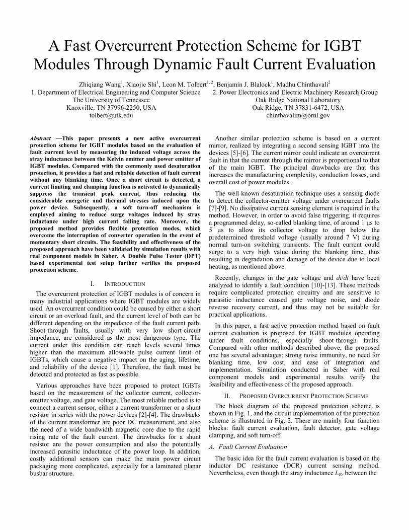
III. SIMULATION VERIFICATION A double pulse test circuit based simulation is done for the
proposed fault protection scheme using real IGBT (CM400DY-12H, 400 A/ 600 V) and other component models in Saber. The simulation circuit is shown in Fig. 7, which represents one phase leg of a three phase inverter with an inductive load. The short circuit control switch, composed by two parallel IGBT modules, is controlled to create a shoot-through fault. The device under test (lower IGBT) could present overcurrent at the turn-on switching transient or during the on-state condition, resulting in hard switching fault (HSF) or fault under load (FUL), respectively [1].
Fig. 7. Simulation circuit in Saber.
Fig. 8 shows the simulation waveforms of gate voltage of the device under test vge, gate voltage of the short-circuit control device vHSF, collector-emitter voltage vce, and collector current ic under HSF condition with the proposed protection scheme. During short circuit transient, the current through the IGBT reaches 1.3 kA quickly, and the turn-off voltage overshoot is around 80 V. When the proposed protection scheme is adopted, the fault current peak is limited to around 500 A, and finally clamped to 300 A in less than 2 μs. The turn-off voltage overshoot is only 20 V.
W/O protectionW/ protection W/O
W/
W/O
W/O
W/
W/
W/ W/O
Fig. 8. Protection circuit operation during a HSF.
Fig. 9 shows the same simulation waveforms under FUL condition. Without the protection circuit, the gate voltage exceeds 15 V due to the displacement current caused by Miller capacitance and high dv/dt. Higher gate voltage results in much higher fault current, which is greater than 2.3 kA. The turn-off voltage overshoot is around 80 V.
When the proposed protection scheme is adopted, the current peak value is significantly reduced to 1 kA within 1 μs and finally clamped to 300 A. The voltage overshoot is reduced to 50 V. In both HSF and FUL cases, the protection circuit responds to the fault quickly, and pulls the device back to its safe operating area.
Fig. 9. Protection circuit operation during a FUL.
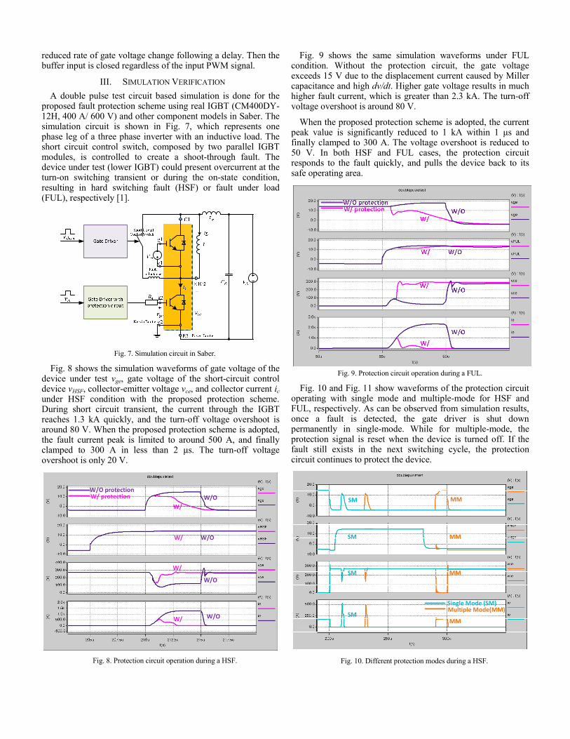
Fig. 10 and Fig. 11 show waveforms of the protection circuit operating with single mode and multiple-mode for HSF and FUL, respectively. As can be observed from simulation results, once a fault is detected, the gate driver is shut down permanently in single-mode. While for multiple-mode, the protection signal is reset when the device is turned off. If the fault still exists in the next switching cycle, the protection circuit continues to protect the device.
Single Mode (SM)Multiple Mode(MM)
SM
SM
SM
SM
MM
MM
MM
MM
Fig. 10. Different protection modes during a HSF.

Fig. 11. Different protection modes during a FUL.
IV. EXPERIMENTAL VERIFICATION Experimental results are presented for an IGBT module using
the proposed protection method. The test setup is shown in Fig. 7. The device used for the experimental test is a 600 V, 400 A Powerex IGBT module (CM400DY-12NF). The experimental waveforms are recorded by a Tektronix DPO5204 2GHz 4 channel Digital Phosphor Oscilloscope. The voltage was measured with a calibrated active high voltage probe Tektronix P5205 with 100 MHz bandwidth. The collector current was measured by a T&M Research SSDN-015 coaxial shunt with resistance of 0.015 Ω and high bandwidth of 1.2 GHz. The switching energy loss is calculated using the math function of the oscilloscope.
The actual test bed is shown in Fig. 12. The IGBT module and DC capacitor bank are connected by an internal planar busbar structure within the PCB board. The overcurrent (OC) protection board is integrated together with the turn-on and turn-off active gate driver (discussed in [15]).
Fig. 12. Experimental testbed for verification of the protection scheme.
The experimental results of overload, hard switching fault, and fault under load are presented with a DC bus voltage of 300 V. The protection threshold for overload is set to 200 A by tuning Cf = 1 nF and Rf = 500 Ω, and for short-circuit is set to 300 A by tuning Cf = 1.5 nF and Rf = 500 Ω.
Fig. 13 shows the waveforms of gate voltage of the device under test vge, output of the short-circuit detector vpt, collector-emitter voltage vce, and collector current ic under overload condition with the proposed protection scheme.
When the current flowing through the IGBT exceeds 200 A, the output of the short-circuit detector changes instantaneously and remains at high level. The high level output activates the capacitor Cz and Zener diode Dz to suppress the current peak and finally clamp the current at the expected level. In the overload protection test, the gate voltage is clamped at 9.5 V, with a current of 85 A. The clamping current level can be easily changed by using different Zener diodes.
Fig. 13. Experiment test setup.
Fig. 14 shows the gate voltage of the device under test vge, gate voltage of the short-circuit control device vHSF, collector-emitter voltage vce, and collector current ic under HSF condition with the proposed protection scheme. The fault current peak is limited to 505 A within 0.75 μs, and then it is clamped to 292 A, with a corresponding clamped gate voltage of 10.7 V. When the clamped current settles down after 2 μs, it was softly turned off with a voltage overshoot of 20 V.
Fig. 14. Protection waveforms under HSF.
Fig. 15 (a) and Fig. 15 (b) show waveforms of input PWM signal vin, short-circuit PWM signal vshort, collector-emitter
IGBT Module
Inductor Connector
DC link
Coaxial Shunt
DC Power Supply Input
Turn-off ControlTurn-on Control
OC Protection
vce (100V/div)
ic (53A/div)
vge (5V/div)
vpt (5V/div)
Vge= 9.5V
Iclamp= 85A
Ipt=200A
t (1 μs/div)
vce (100V/div)
ic (133A/div)
vge (10V/div)
vHSF (10V/div)
Vge= 10.7V
Iclamp= 292A
Ipeak=505A
t (2 μs/div)0.75 μs

voltage vce, and collector current ic when the protection circuit is operating in single mode and multiple-mode under HSF, respectively. As can be observed, once a fault is detected, the gate driver is shut down in single-mode, despite the change of short-circuit PWM signal. While for multiple-mode, the fault is protected cycle-by-cycle, and automatically resets before the next 'on' cycle. When the short-circuit PWM signal is cleared in the third pulse, as shown in Fig. 15 (b), the gate driver is restarted. The gate driver continues to work until a shutdown command is received.
(a) Single mode
(b) Multiple mode
Fig. 15. Different protection modes under HSF.
A similar test is done under FUL condition with the protection scheme. Fig. 16 illustrates the gate voltage of the device under test vge, gate voltage of the short-circuit control device vFUL, collector-emitter voltage vce, and collector current ic. The fault current peak is limited to 1150 A within 1.1 μs, which is much higher than that of the HSF, due to the high dv/dt induced displacement current flowing through Miller capacitance as well as internal gate resistance. The clamping capacitor CZ continuously draws current from the gate capacitance and buffer, until the gate voltage is clamped at 10.7 V by Zener diode DZ. Hence, both the gate voltage and current waveform present a noticeable notch. The clamped current is
safely turned off with a voltage overshoot of 70 V. Large CZ capacitance would decrease the current peak; however, it would also increase the voltage overshoot.
Fig. 16. Protection waveforms under HSF.
(a) Single mode
(b) Multiple mode
Fig. 17. Different protection modes under FUL.
Fig. 17 (a) and Fig. 17 (b) show waveforms of the input PWM signal vin, short-circuit PWM signal vshort, collector-emitter voltage vce, and collector current ic when the protection
vce (100V/div)
ic (133A/div)
vin (5V/div)
vshort (5V/div)
t (20 μs/div)
vce (100V/div)
ic (133A/div)
vin (5V/div)
vshort (5V/div)
t (20 μs/div)
vce (100V/div)
ic (266A/div)
vge (10V/div)
vFUL (10V/div)
Vge= 10.7V
Iclamp= 310A
Ipeak=1150A
t (2 μs/div)1.1 μs
vce (100V/div)
ic (266A/div)
vin (5V/div)
vshort (5V/div)
t (20 μs/div)
vce (100V/div)
ic (266A/div)
vin (5V/div)
vshort (5V/div)
t (20 μs/div)

circuit is operating in single-mode and multiple-mode under FUL, respectively. In single-mode, the gate driver is shut down once a fault is detected in the first input PWM pulse. The fault still exists in the second pulse and disappears in the third one. In multiple-mode, the fault current is protected cycle-by-cycle until the fault is cleared or shut down after a certain number of faults are counted within a set time period.
V. CONCLUSION A novel overcurrent protection scheme is presented which
could protect an IGBT module against overload condition as well as HSF and FUL transients. This proposed circuit provides a fast and reliable detection of IGBT fault current without blanking time. Both simulation and experimental results verify that the proposed scheme could effectively limit the dynamic short circuit peak current, clamp the fault current to a safe level, and suppress voltage overshoot of a shutdown transient. Additionally, flexible operation mode of this protection scheme is beneficial for avoiding interruption of the converter operation, as in the case of momentary short circuits.
ACKNOWLEDGEMENT This work was partially funded by the II-IV Foundation and
Oak Ridge National Laboratory under the U.S. Department of Energy’s Vehicle Technologies Program. This work made use of Engineering Research Center Shared Facilities supported by the Engineering Research Center Program of the National Science Foundation and DOE under NSF Award Number EEC-1041877 and the CURENT Industry Partnership Program.
REFERENCES [1] R. S. Chokhawala, J. Catt, and L. Kiraly, “A discussion on IGBT short-
circuit behavior and fault protection schemes,” IEEE Transactions on Industry Applications, vol. 31, no. 2, pp. 256-263, Mar. 1995.
[2] F. Huang and F. Flett, “IGBT fault protection based on di/dt feedback control,” IEEE Power Electronics Specialists Conference, 2007, pp. 1478-1484.
[3] L. Zuo, S. K. Islam, M. A. Huque, C. Su, B. J. Blalock, and L. M. Tolbert, “A universal BCD-on-SOI based high temperature short circuit protection for SiC power switches,” International Conference and Exhibition on High Temperature Electronics, Albuquerque, New Mexico, USA, May 13-15, 2010.
[4] V. Bolloju and J. Yang, “Influence of short circuit conditions on IGBT short circuit current in motor drives,” in IEEE Applied Power Electronics Conference and Exposition, 2011, pp. 1675-1679.
[5] M. Kudoh, Y. Hoshi, S. Momota, T. Fujihira, and K. Sakurai, “Current sensing IGBT for future intelligent power module,” IEEE International Symposium on Power Semiconductor Devices and ICs, 1996, pp. 303-306.
[6] B. Lu and S. K. Sharma, “A literature review of IGBT fault diagnostic and protection methods for power inverters,” IEEE Transactions on Industry Applications, vol. 45, no. 5, pp. 1770-1777, Sep. 2009.
[7] V. John, B. Suh, T. A. Lipo, “Fast-clamped short-circuit protection of IGBT's,” IEEE Transactions on Industry Applications, vol. 35, no. 2, pp. 477-486, 1999.
[8] Z. Xu and F. Wang, “Experimental investigation of Si IGBT short circuit capability at 200°C,” IEEE Applied Power Electronics Conference and Exposition, 2012, pp. 162-168.
[9] L. Chen and F. Z. Peng, “Active fault protection for high power IGBTs,” IEEE Applied Power Electronics Conference and Exposition, 2009, pp. 2050-2054.
[10] M. A. Rodríguez-Blanco, A. Claudio-Sánchez, D. Theilliol, L. G. Vela-Valdés, P. Sibaja-Terán, L. Hernández-González, and J. Aguayo-Alquicira, “A failure-detection strategy for IGBT based on gate-voltage behavior applied to a motor drive system,” IEEE Transactions on Industrial Electronics, vol. 58, no. 5, pp. 1625-1633, May. 2011.
[11] M. A. Rodriguez, A. Claudio, D. Theilliol, and L. G. Velan, “A new fault detection technique for IGBT based on gate voltage monitoring,” IEEE Power Electronics Specialists Conference, 2007, pp. 1001-1005.
[12] J. Lee and D. Hyun, “Gate voltage pattern analyze for short-circuit protection in IGBT inverters,” IEEE Power Electronics Specialists Conference, 2007, pp. 1913-1917.
[13] L. Pierre, B. Dominique, M. Herve, A. Bruno, and R. Jean-Francois, “Fast over-current protection of high power IGBT modules,” European Conference on Power Electronics and Applications, 2005, pp. 1-10.
[14] L. Pierre and B. Dominique, “State of the art of dv/dt and di/dt control of insulated gate power switches,” Power Supply and Energy Management for Defence Applications, 2007, pp. 1-8.
[15] Z. Wang, X. Shi, L. M. Tolbert, and B. J. Blalock, “Switching performance improvement of IGBT modules using an active gate driver,” in IEEE Applied Power Electronics Conference and Exposition, 2013, 8 pages.