A Data Processing Subsystem for the Holo-Chidi Video ...
76
A Data Processing Subsystem for the Holo-Chidi Video Concentrator Card by Aditya Prabhakar S.B. Electrical Engineering and Computer Science Massachusetts Institute of Technology, 2000 Submitted to the Department of Electrical Engineering and Computer Science in Partial Fulfillment of the Requirements for the Degree of Master of Engineering in Electrical Engineering and Computer Science at the Massachusetts Institute of Technology August 30, 2001 © 2001 Massachusetts Institute of Technology All rights reserved Signature of Author....................... Department of Electri Engineering and ARCHIVeS MASSACHUSETTS INSTITUTE OF TECHNOLOGY JUL 3 1 2002 LIBRARIES Computer Science August30, 2001 Certified by................................ V Stephen A. Benton E. Rudge and Nancy Allen Professor of Media Arts and Sciences Thesis Supervisor Accepted by.................... ....... Arthur C. Smith Chairman, Department Committee on Graduate Theses Department of Electrical Engineering and Computer Science
Transcript of A Data Processing Subsystem for the Holo-Chidi Video ...

A Data Processing Subsystem for the Holo-ChidiVideo Concentrator Card
by
Aditya Prabhakar
S.B. Electrical Engineering and Computer Science
Massachusetts Institute of Technology, 2000
Submitted to the Department of Electrical Engineering and Computer Science in PartialFulfillment of the Requirements for the Degree of
Master of Engineering in Electrical Engineering and Computer Science
at the
Massachusetts Institute of Technology
August 30, 2001
© 2001 Massachusetts Institute of TechnologyAll rights reserved
Signature of Author.......................Department of Electri Engineering and
ARCHIVeSMASSACHUSETTS INSTITUTE
OF TECHNOLOGY
JUL 3 1 2002
LIBRARIES
Computer ScienceAugust30, 2001
Certified by................................ V
Stephen A. BentonE. Rudge and Nancy Allen Professor of Media Arts and Sciences
Thesis Supervisor
Accepted by.................... .......Arthur C. Smith
Chairman, Department Committee on Graduate ThesesDepartment of Electrical Engineering and Computer Science

A Data Processing Subsystem for the Holo-ChidiVideo Concentrator Card
by
Aditya Prabhakar
Submitted to theDepartment of Electrical Engineering and Computer Science
Aug. 30t, 2001
In Partial Fulfillment of the Requirements for the Degree ofMaster of Engineering in Electrical Engineering and Computer Science
Abstract
A specialized board was designed to improve the performance of the Mark-IIHolographic Video system. Acting as a high speed-frame buffer, the Video ConcentratorCard takes in a computed holographic frame, stores it in Video RAM, and formats andsends the data out to the display in analog form. In conjunction with the Avid JupiterHD card, the two sets of cards would make up Holo-Chidi. Holo-Chidi is designed to bea stable and efficient method for delivering computed holographic fringes to theHolovideo system in real-time. A data processing system, the Data Handler, wasdeveloped to handle all the control signals on the board. Using programmable logic, thebasic framework on the Data Handler was developed. Initialization processes weredeveloped, as well as access process for the various components on the board.
This research was funded by the Digital Life Consortium at the MIT Media Laboratory.
Thesis Supervisor: Dr. Stephen A. Benton,
Title: E. Rudge and Nancy Allen Professor of Media Arts and Sciences, MIT Media Laboratory
Project Supervisor: Dr. Thomas A. Nwodoh
Title: Research Associate, Spatial Imaging Group, MIT Media Laboratory
2

Acknowledgements
This thesis would not have been possible without the support, guidance, and assistance ofmany people.
First, I would like to thank Prof. Stephen Benton for giving me the opportunity to workon such a challenging project such as Holo-Chidi. His holography class opened up awhole new and exciting field, which I had never known to exist. Through his support, Iwas able to do my part in contributing to the field of holography, by working on theHolographic Video system.
Dr. Thomas Nwodoh also deserves my thanks for allowing me to work on the Holo-Chidiproject. Through his guidance and assistance, I was able to develop my skills as ahardware designer from all aspects. Without his help, this project would not have beenpossible. I appreciate the patience he had with me, as I struggled to find solutions to themany problems in the Data Handler design. I also must thank him sincerely for being thechief editor for this document, making sure I had all my facts about the design correct.
Elroy Pearson, my fellow thesis survivor and officemate, provided me with no end ofentertainment and support. He was always willing to listen to me babble on about finitestate machines and timing diagrams. Elroy's assistance was invaluable in helping meformulate my design ideas, and also in helping me keep my sanity. I know this thesiswould not have been possible if Elroy had not been there to help me whenever I neededit.
To the rest of the Spatial Imaging group, I want to thank them for their extensiveknowledge and wisdom. I have learned a great deal about the field of holography fromthem. They lent their ears to a stressed graduate student, and provided me a supportivenetwork of friends.
To my fellow M. Engers, Ashwinder Ahuluwalia, Jason Sharma, and John Paul Strachan,I express my gratitude for keeping me entertained, as I struggled to complete my work.Their camaraderie, whether it be from late night foosball escapades, or stiff video gamecompetitions, helped to boost my confidence, even in the worst days of my research. Aspecial thanks goes to Ash and Jason for keeping a roof over my head in my last weekhere at MIT.
To all of my old roommates, Spencer Liang, Danny Lai, and Bhuwan Singh, I do notbelieve I have met a nicer group of people. Your friendship through the years has helpedme achieve my goals, and then some. Thank you for putting up with me, just like allbrothers do. I want to add that this thesis would never have been printed were it not forthe help of Mr. Singh.
To all my Boston B-boys and girls out there, I want to thank you for keeping me in shape,after hours of sitting in front of my computer. I will return.
3

To my sister, Pavitra Prabhakar, words cannot express how much her support has meantto me over the years. I would never have been able to accomplish all that I have, withouther guidance and support.
To my parents, Padmini and R. Prabhakar, deserve more gratitude than I can ever give.They gave me the unconditional support I needed to survive all that I have been throughat this school. Nothing I have ever accomplished could have been achieved withoutthem. Through their belief in me and what I could achieve, I have become the man that Iam today. Thank you from the bottom of my heart.
I could not have completed the work of this thesis without the support of these people,and many others, who I may have forgotten to mention. I am in your debt. Thank youfor making my time at MIT an experience I will never forget.
4
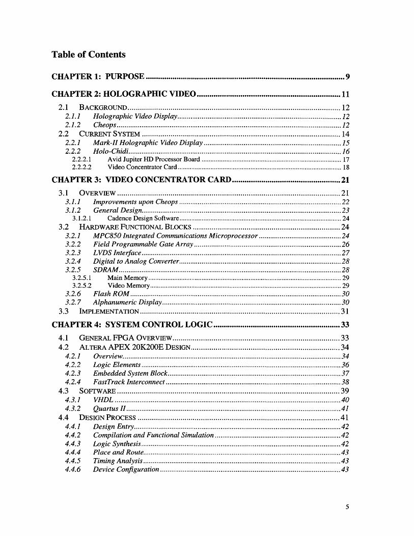
Table of Contents
CH A PTER 1: PU R PO SE ............................................................................................ 9
CHAPTER 2: HOLOGRAPHIC VIDEO.....................................................................11
2.1 BACKGROUND ..................................................................................................... 122.1.1 Holographic Video Display................................................................................... 122.1.2 Cheops......................................................................................................................12
2.2 CURRENT SYSTEM ............................................................................................. 142.2.1 M ark-II Holographic Video Display ..................................................................... 152.2.2 Holo-Chidi................................................................................................................16
2.2.2.1 Avid Jupiter HD Processor Board ............................................................................. 172.2.2.2 Video Concentrator Card........................................................................................... 18
CHAPTER 3: VIDEO CONCENTRATOR CARD....................................................21
3.1 OVERVIEW ......................................................................................................... 213.1.1 Improvements upon Cheops ................................................................................ 223.1.2 General Design..................................................................................................... 23
3.1.2.1 Cadence Design Software......................................................................................... 243.2 HARDW ARE FUNCTIONAL BLOCKS..................................................................... 24
3.2.1 MPC850 Integrated Communications Microprocessor ........................................ 243.2.2 Field Programmable Gate Array ......................................................................... 263.2.3 LVDS Interface.................................................................................................... 273.2.4 D igital to Analog Converter................................................................................. 283.2.5 SDRAM ..................................................................................................................... 28
3.2.5.1 M ain M emory ............................................................................................................... 293.2.5.2 Video M emory.............................................................................................................. 29
3.2.6 Flash ROM ............................................................................................................... 303.2.7 Alphanumeric Display......................................................................................... 30
3.3 IM PLEMENTATION .............................................................................................. 31
CHAPTER 4: SYSTEM CONTROL LOGIC.............................................................33
4.1 G ENE RA FPG A OVERVIEW ................................................................................. 334.2 A LTERA A PEX 20K 200E D ESIGN........................................................................ 34
4.2.1 Overview................................................................................................................... 344.2.2 Logic Elements.................................................................................................... 364.2.3 Embedded System Block....................................................................................... 374.2.4 FastTrack Interconnect ....................................................................................... 38
4.3 SOFTW ARE ............................................................................................................ 394.3.1 VHDL ....................................................................................................................... 404.3.2 Quartus II ................................................................................................................. 41
4.4 D ESIGN PROCESS ............................................................................................... 414.4.1 Design Entry ............................................................................................................. 424.4.2 Compilation and Functional Simulation .............................................................. 424.4.3 Logic Synthesis..................................................................................................... 424.4.4 Place and Route................................................................................................... 434.4.5 Timing Analysis .................................................................................................... 434.4.6 Device Configuration........................................................................................... 43
5

CHAPTER 5: DATA HANDLER SYSTEM IMPLEMENTATION...........45
5.1 G ENERAL D ESIGN .............................................................................................. 455.1.1 Top-level D esign................................................................................................... 455.1.2 Common D esigns................................................................................................... 47
5.1.2.1 Finite State M achine .................................................................................................. 475.1.2.2 Counters........................................................................................................................ 495.1.2.3 Bidirectional Signals.................................................................................................. 505.1.2.4 Flip-flops ...................................................................................................................... 51
5.1.2 System D ebugging .................................................................................................... 515.2 SYSTEM INITIALIZATION ....................................................................................... 52
5.2.1 Design Overview .................................................................................................. 525.2.2 Timing Analysis.................................................................................................... 53
5.3 ALPHANUMERIC DISPLAY PORT PROGRAMMING .............................................. 545.3.1 Design Overview .................................................................................................. 545.3.2 Timing Analysis..................................................................................................... 58
5.4 PROCESSOR Bus CONTROL ................................................................................. 585.4.1 Design Overview .................................................................................................. 585.4.2 Timing Analysis..................................................................................................... 60
5.5 FLASH RO M IMPLEMENTATION............................................................................605.5.1 Data Retrieval .......................................................................................................... 60
5.5.1.1 Design Overview ...................................................................................................... 615.5.1.2 Timing Analysis ........................................................................................................... 62
5.5.2 Creating a ROM ................................................................................................... 635.6 SD RA M CO m OL...............................................................................................63
5.6.1 SDRAM Initialization ............................................................................................ 63.5.6.1.1 Design Overview ...................................................................................................... 635.6.1.2 Timing Analysis ........................................................................................................... 66
5.6.2 SDRAM W rite ........................................................................................................... 665.6.2.1 Design Overview ...................................................................................................... 665.6.2.2 Timing Analysis ........................................................................................................... 68
5.7 CURRENT SYSTEM STATUS...................................................................................69
CHAPTER 6: CONCLUSION.................................................................................. 71
6.1 FUTUREW ORK ................ ..... .. . ..... ................................... 71
APPENDIX A: MPC850 BUS ARBITER SIGNALS.............................................73
EN D N O TES ..................................................................................................................... 75
6

Figures
FIGURE 1: OVERVIEW OF A HOLOVIDEO SYSTEM' .............................................................. 11FIGURE 2: CHEOPS SYSTEM ARCHITECTURE 3 . . . . . . . . . . . . . . . . . . . . . . . . . . . . . . . . . . . . . 13
FIGURE 3: OVERVIEW OF THE MARK-II HOLOVIDEO DISPLAY2.......................................... 15FIGURE 4: BASIC LAYOUT OF THE HOLO-CHIDI SYSTEM................................................. 17FIGURE 5: GENERAL BLOCK DIAGRAM FOR VIDEO CONCENTRATOR CARD.................... 22FIGURE 6: BLOCK DIAGRAM OF THE MPC8509................................ . . . . . . . . . . . . . . . .. . . . . . . . . . . . . 25
FIGURE 7: LVDS RECEIVER BLOCK DIAGRAM" ........................................................... 27FIGURE 8: ALPHANUMERIC DISPLAY BLOCK DIAGRAM15 ............................ 30FIGURE 9: APEX 20K200E DEVICE BLOCK DIAGRAM10 . . . . . . . . . . . . . . . . . . . .. . . . . . . 35FIGURE 10: APEX 20K200E LOGIC ELEMENT' 0. . . . . . . . . . . . . . . .. . . . . . . . 36FIGURE 11: APEX 20K200E ESB IN INPUT/OUTPUT CLOCK MODE' 0 . . . . . . . . . . . . . . . . 38FIGURE 12: APEX 20K200E FASTROW INTERCONNECT' 0 .................. . . . . . . . . . . . . . . . . . . . . . . . . . . . 39FIGURE 13: FPGA DESIGN FLOW .................................................................................. 41
FIGURE 14: GENERAL STRUCTURE OF THE DATA HANDLER SYSTEM.............................. 46
FIGURE 15: GENERAL DESIGN FOR MOORE MACHINE FSM........................................... 48
FIGURE 16: STATE DIAGRAM FOR SYSTEM INITIALIZATION ........................................... 52FIGURE 17: STATE DIAGRAM FOR ALPHANUMERIC DISPLAY PORT PROGRAMMING .......... 56FIGURE 18: STATE DIAGRAM FOR BUS CONTROL MODULE ............................................ 59FIGURE 19: STATE DIAGRAM FOR ROM DATA READ MODULE ......................................... 61FIGURE 20: STATE DIAGRAM FOR SDRAM INITIALIZATION ............................................. 64FIGURE 21: STATE DIAGRAM FOR SDRAM WRITE MODULE ............................................ 67
Tables
TABLE 1: APEX 20K200E DEVICE FEATURES '0 ............................. . . . . . . . . . .. . . . . . . . . . . . . . . . . . . . . . . . 35
TABLE 2: MAPPING OF DATA, ALPHANUMERIC DISPLAY DATA, AND HEXIDECIMAL VALUES 15
............. ................................ .............. 54TABLE 3: COMMANDS AND CONTROL SIGNALS FOR THE VCC SDRAM'.......... . . . . . . . . . . . 65TABLE 4: MPC850 BUS ARBITER CONTROL SIGNALS DESCRIPTIONS9 ........... . . . . . . . . . . . . . . . . 73
7

8

Chapter 1: PurposeThis Master's Thesis focuses on the issues related to the design, implementation,
and verification of a data-managing system, or Data Handler (DH). DH is the control
system for the Video Concentrator Card (VCC). It manages the control logic and
controls all the 1/0 chips on the board. The VCC acts in a similar fashion to a frame
buffer contained in all video cards for the modem PC. The purpose of this design is to
ensure that high bandwidths of data generated from multiple processor cards are
transmitted to the VCC, formatted, buffered, and then passed properly to the outputs. All
these design points must occur as efficiently as possible, avoiding any timing issues, such
as data contention and in conformity with valid setup and hold times (tsu and thold
respectively). Together, these design points and efficiency considerations create a very
vast and complex system. While many commercial frame buffer cards exist in today's
market, none can handle the magnitude of the bandwidth or processing power for the
target system of this design: holographic video (Holovideo).
The material contained in this thesis is divided into 4 main chapters. The first
chapter describes the holovideo system and how the VCC fits into that system. This
section describes the predecessor system to VCC, or CHEOPS. The main focus of the
second chapter is the general design of the VCC, with a look into the key components
design of this system. The third chapter describes techniques for designing and
developing a control logic system: the materials with which to create one, the
methodology behind complex logical systems, in depth descriptions of the language used
to create DH, and the chip on which the design will fit. Finally, the focus shifts to the
actual development of DH. Its main modules are discussed in full, from design to
implementation to verification.
The magnitude of this project is fairly vast. During the initial design stages, the
schematics and layout notes were created, and a netlist was generated. Then the project
shifted to acquisition of all the components that are contained in VCC. The components
and designs were then sent out to an independent contractor for layout, fabrication, and
assembly. Upon its return, the simulated designs of DH were tested in the actual board.
This field-testing of DH created a greater understanding on how to create a "safe" design,
9

that while efficient, contains enough redundancy to eliminate possible errors that
improper control logic can create.
The main scope of this thesis is to describe how to create modules for a data-
management system. It gives a description of the requirements of the system, how to
implement the system, and the actual design of that system. The system itself is divided
into seven main modules, some containing several sub-components. The interaction of
these modules is essential for the creation of a functioning system, while allowing it to be
as easy as possible for future designers to understand. The thesis concludes with some
potential research areas that can be pursed using the components outlined in this thesis.
10

Chapter 2: Holographic VideoHolographic video is an electronic imaging system that can render and display
computer generated holograms at near-video rates. Holographic video was developed by
Dr. Stephen A. Benton et. al. at the MIT Media Lab in the late 1980's.' The Mark-II
Holovideo display is the current generation of that initial work.
Overview of a Holovideo System
3-D Image
Ik Viewer
Fringe DisplayComputation System.
User Interface,
Content processing
Figure 1: Overview of a Holovideo System'
Dr. Benton's group developed the Mark-Il system in the early 1990's.2 The system is
capable of producing 36-MB images as large as about 150 mm in width, 75 mm in height,
and 100 mm depth. The computation involves transforming a 3-D numerical description
of the object scene into a holographic fringe pattern.
Unfortunately, many of the possible avenues of research for this system have yet
to be explored, due to the fact that the computational tools, modulation tools and the
communication bandwidth are limited. Imagine having a holographic television in your
home, or a cardiologist having the ability to look at a moving holographic representation
of a patient's heart to "see" if any problem areas exist. These potentials cannot be
accessed by the system that currently exists. The main bottleneck for this system is the
computation hardware that is connected to the Content Processing, between the user
interface and the fringe computation. To tap the potential of holovideo, its hardware
needs to be upgraded beyond its current specifications, to allow for faster computation
and rendering.
11

2.1 Background
2.1.1 Holographic Video Display
The initial work on electronic holography began in 1987 at the MIT Media Lab.
It was not until 1989, before the researchers were able to display simple geometric
patterns on the holographic display. At that time, only horizontal scan lines of low
spatial resolution were available for the display. This system only supported a single
channel, on which 2MB of data could be transmitted. By 1990, an increase in the number
of scan lines allowed a higher resolution hologram to be displayed, while three channels
of data could be supported. The following year, further progress was made, as the
display could support color images. In 1992, additional channels were added to the
display. It could now display 36 MB of data, transmitted through 18 channels, or holo-
lines, as they were called. This became available through the use of a new image
processing system, known as Cheops. Cheops had a large reconfigurable frame buffer
and also contained hardware for computing holographic data. Using this large amount of
data, the viewing size and image volume of the display were greatly increased, creating a
convincing 3-D image. 3 This version is the current model being used for research at the
MIT Media Lab.
2.1.2 Cheops
The hardware that supplies the appropriate data to the holographic display is
known as Cheops. Cheops was developed by the Information and Entertainment group at
the MIT Media Lab in 1995. The Cheops Imaging System is a compact, modular
platform for acquiring, processing, and displaying video sequences and model-based
representations of moving scenes. This hardware allowed the user to perform several
different operations on streaming data, a task, when left to software, is incredibly
computationally intensive. It has the ability to perform these tasks in parallel by using
dynamic scheduling of resources. It also contains buffers that enable slower-than-real-
time processing of data, when the demand for data exceeds the resources available. This
quality made it an ideal choice for use with the Holovideo system, which requires a
efficient and flexible frame buffer for outputting holographic data.
12

The Cheops system is composed of three modules: processor, input/memory, and
output. These modules are interconnected with three linear data buses. Two buses are
capable of performing high bandwidth transfers (>100Mbyte/sec) of pixel rasters (the
Nile Buses) and the third is a 32Mbyte/sec bus supervisory control of the 1/0 modules by
the processor (the Global Bus). The system also contains 8 blocks of video random
access memory (VRAM), which is used to store data before it is processed. Data is
accessed from the VRAM and sent to specialized stream processors for manipulation or
computation. The properly modified data is then sent back into a separate portion of
VRAM, where it waits to be outputted.
Analog or DigitalVideo In
Input/Memory Module(s)Processr(up to 4)
OR-Processor Module(s)(up to 4)
I'
41tNile Buses I & 2large blocks ofordered data(e.g. rasters)such 48 bits wide,25M tran sferalsec
Output Module(s)(up to 4)
Analog or DigitalVideo Out
'High.Speed
HostComputer
(SCSIRSn232)
Global Buscontrol andgeneral datacommunications32 bits wide,8M tran sforslsec
Figure 2: Cheops System Architecture4
Through some modifications to the programmable array logic chips (PALs) used
on the Cheops and in the display software, it became a suitable component of the
Holovideo system. It provided six synchronized frame buffers to drive the 256Kx 144
13
A
*
*
1-400

display as well as a high speed interface to host processors and a local data-flow
processing card for decoding of encoded or compressed image formats. Each Cheops
framebuffer board contained 3 output channels, which allowed 6 boards to support 18
holo-lines. Each channel includes a digital to analog converter (DAC) with 8 bits of
resolution. Each of these channels access 2.1 Mbytes of data that are outputted from the
VRAM. The 6 boards allow the system to process 36 MB holographic frames. The data
rate on the output was 110 MB/s.
With the need for high-speed data transfer systems, as well as the availability of
faster technology, the current Cheops system is no longer satisfactory for any expansion
of the Holovideo system. Until a faster architecture is in place, future research will be
severely hindered. The current programs that are contained on Cheops require out-of-
date Legacy operating systems in order to compile them. In addition to these issues, the
temperature sensitive nature of the boards requires large air-conditioners to be constantly
on, though the boards will continue to crash on occasion. All of these problems have been
a driving force in pushing for the development of a new, faster system that is reliable and
allows for holograms to be displayed and edited in real-time.
2.2 Current System
The holographic display that currently exists is composed of the aging Cheops
system and the Mark-II Holographic Video Display. The system is capable of producing
36-MB images as large as about 150x75x100 mm in width, height, and depth.
Computation involves transforming a 3-D description of the object scene into a
holographic fringe pattern. This information is then transferred to the optical setup where
the fringe patterns can actually be displayed through a specialized system designed to
diffract and focus laser light.
14
2.2.1 Mark-II Holographic Video Display
The Mark-fl Holovideo display was designed to exploit parallelism whenever
possible, both optically and electronically, such that the approach could be expanded to
arbitrarily large image sized displays. To achieve the goal of a 150x75xI00mm image,
two 18-channel Acousto-Optic Modulators (AOM) were used, with each channel of a
single AOM modulating beams of red light (X = 633nm) in parallel.5 An AOM is a
crystal combined with an ultrasonic transducer that converts the complex fringe pattern
required for holography into an optical beam. The AOM takes in RF signals as an input,
where upon six tiled horizontal mirrors scan across matched to the speed of the signal in
the AOM, such that it appears the diffraction pattern in the AOM is stationary. These RF
signals come from an RF processor that takes the analog output of Cheops and converts it
into usable signals.
U
U U
rnc4uI~Ir~r5
Figure 3: Overview of the Mark-I Holovideo display 2
As the mirrors scan from left to right, one AOM provides 18 lines of rastered
image. When the mirrors return from right to left, the second cross-fired AOM provides
the next 18 lines of rastered image. A vertical scanner images each 18-line pass below the
previous one, with 8 horizontal scans in all, providing 18x8=144 vertical scan lines.
The resulting image is horizontal parallax only (HPO), with video resolution in
the vertical direction, and holographic resolution in the horizontal direction, with a 30-
15
MM

degree view zone. A HPO image does not require as much information to generate,
making it a good choice for Holovideo where information efficiency is important. In
order to avoid flickering on the screen, the display must be refreshed at a minimum
refresh rate of 30 frames/s. Standard television signals refresh at 60 frames/s. A frame
image consists of 36 million samples. Thus the minimum required rate of samples per
second is 1.14 billion.2 Since it was currently impossible to create that sample rate,
Cheops, with its parallel architecture was used to approach the desired rate. The analog
signal needs to have a bandwidth of 55Mhz. Cheops uses a sampling rate of 110Mhz
ensuring an output sample with no aliasing, since the sampling rate will be at the Nyquist
rate.6 Each horizontal line of the display is 256-thousand pixels of holographic fringe
pattern translating to 36Mbytes of information per frame, fed at a total data rate of
2Gpixels/sec into the display from the frame buffers.
2.2.2 Holo-Chidi
The new processor and video concentrator cards, that can handle the demand for
the computation and data transfer necessary for the increasing demands placed on
Holovideo, is known as Holo-Chidi. Chidi is the name of a Nigerian god, from which the
system derives its name. Currently in development, this system will ultimately replace
the Cheops processing system. Holo-Chidi will have the all the functionality of Cheops,
while being more efficient, scalable and stable. The system, when fully integrated, will
make development of complicated holographic images a possibility, allowing for
binocular and monocular cues to a viewer. Eventually, it will be able to accept
standardized holographic description files, and through internal computation of the
holographic fringe patterns, provide the appropriate data for the Mark-II system. The
addition of an additional piece of hardware enabled Cheops to compute holographic
fringes. Due to the limited speed of that hardware, the limited system does not allow for
the ability to modify or edit these holograms in real-time. Development is currently
underway for the system hardware that will scale-up the computational capacity of
multimedia processors and ultimately lead to real-time rendering for and computation of
computer-generated holographic stereograms and holographic frames of moving scenes
at video rates.
16

The Holo-Chidi system will be used for hologram computation, data archival/retrieval
to/from a host system, and for the control of the Mark-Il. It is composed of two main
components: the set of Avid Jupiter HD processor cards and the display interface cards,
known as the video concentrator cards.
-----------------------.HOSTO
LV-Id 0 O t
F AvidUSART 0aes-5
HOST 1
Output .
V Cardt
S Avid 45ar
* __j________
HOLO-CHIDI
Figure 4: Basic Layout of the Holo-Chidi system
A Holo-Chidi system with nine Avid PCI processor cards and three display
interface cards can perform over two billion superposition (8 bit multiplication and 21 bit
addition) operations in one second. This throughput is enough to compute a 36MB
hologram frame in less than 0.6 seconds (worst case, for a hologram with only non-zero
values in its input data) and in lesser time for a hologram with sparse input data. The
system can also display the computed holograms at video refresh rates. This will enable
research in more computationally expensive algorithms, such as for full color holograms,
or ideally, full-motion holograms.
2.2.2.1 Avid Jupiter HD Processor Board
The Avid boards, which will ultimately total nine in a Holo-Chidi
implementation, were initially developed for the high definition television (HDTV)
market. It was designed to interface with HD software that provides HD-capable
17

compositing, effects, titling, and editing systems. The board contains a LVDS serial
digital interface with one input and two outputs, allowing simultaneous feeds to two
devices without loop-through. The similarities in the computation complexity of HDTV
and holograms made this board an ideal fit for Holo-Chidi. The Avid HD system is
capable of digitizing and recording uncompressed HDTV in real time.7 Utilizing the full
editing abilities of this board, holovideo will be able to display larger, more complex
holographic images that can be modified in real-time, as the display is being viewed. The
main fringe computation for the real-time display will take place on this card. It will be
modified to compute holographic stereograms by linearly superposing pre-computed
fringe elements and rendered parallax views of a scene.' The computed video data output
from the boards will need to be multiplexed together in order to pass the data efficiently
to the Mark-II. The video concentrator card will accomplish this task using a high-speed
parallel 1/0 port synchronized with a common clock signal for the entire system.
2.2.2.2 Video Concentrator Card
The display interface card, or Video Concentrator Card (VCC), formats computed
holographic data and converts it to RF analog form to feed the Acousto-Optic-Modulators
of the Mark-II holographic display system. The system has a data- encoding throughput
of up to 5 GigaBytes per second and will ultimately be capable of computing/rendering a
hologram of a moving scene at video rates. The display system is designed with: a high-
speed 1/0 interface where data is transferred from the Avid processor cards, a set of
FIFOs used to buffer data for the holo-lines being displayed, and digital-to-analog
converters (DAC) that convert the digital fringes to analog form.8 The number of DAC's
will total 18, 6 per card. Each DAC handles one holo-line of data. The first DAC
outputs the value for the first scan line, the second DAC outputs the value for the second
scan line, and so on until the first 18 scan lines are outputted. The first DAC then outputs
the value for the 19th scan lines and so on, until all 144 vertical scan lines are created.
This is only for one frame of the hologram. The system then repeats the process with the
next frame of data.
The data enters the VCC through an LVDS data receiver connected to the LVDS
transmitters of the Avid card. This card contains a high-speed data bus, controlled by a
bus arbiter contained with a processor. This processor could eventually be used to assist
18

in the computation of the holographic fringes. This card will also generate the control
signals using a programmable logic device (FPGA) that will be used to handle all the
signals needed by the chips on the board, as well as used by the scanning mirrors of the
Mark-II. The FPGA is a device, with over 500 thousand system gates, and could
eventually serve as a co-processor on the board, again improving the computational
power of the entire system.
In order to allow for an expansion of the size of the holographic display, these
cards have a highly scalable design. By increasing the number of cards connected to the
system, it will be possible to increase the number of holo-lines, and the size of the actual
holograms, assuming the proper modifications are made to the Mark-II system. This will
not only allow and increase in the display size, but will also enable the possibility of
creating a full color holographic display.
19

20

Chapter 3: Video Concentrator Card
3.1 Overview
The Video Concentrator Card (VCC) is a device that takes computed data, stores
that data and then outputs it as an analog output. The system is being developed by the
Spatial Imaging Group at the MIT Media Lab under the supervision of Dr. Thomas A.
Nwodoh. The main design goals for this system are to:
1) Design a system that can process large amounts of data, like those necessary
for holographic applications.
2) Design a system that can properly interface and control the Mark-II
Holographic Video System.
3) Design a system that has strong computational power that can be incorporated
into future research projects.
4) Implement a highly scalable, efficient, and stable system that utilizes
parallelism whenever possible.
The VCC contains a general purpose processor, as well as a field-programmable gate
array (FPGA) that could eventually be used as a co-processor in the system. They share a
single data and address bus, as well as four blocks of SDRAM memory. The board
communicates with other boards through 2 different inputs, an LVDS interface and a
USB interface. The board also contains 6 analog outputs for communication with the RF
processor of the Mark-II system. These analog outputs are created by 6 digital-to-analog
converters (DACs). Data is supplied to these DACs from either the LVDS connection or
the USB connection. The data is also stored in SDRAM memory blocks that represent
the Video memory of the system. Various FIFO's, buffers, and latches are also placed on
the board in order to ensure stable data and avoid issues like bus contention and glitching
signals. A basic design of the system is shown below.
21

DAC 0
DISPLAYSDRAM 0
(2 of 16M x 1
DAC 1 S..
32 BITS
32 BITS BUFFER 0 32 BITS BUFFER6) 1 /A
(2 OF LVTH16244A) (2 of LVTrH16245)
EPROM and SDRAM 32BT
(512K of FLASH + 128 MB
32 BITS of SDRAM)
(AM29LVO40B +4 SDRAMS)
FIFO 0
(128k X 32-BITS) FPA 32 BITS
32 BITS (APEX 20K200E) 32BT
LATCH 0 LATCH 1
(VTH1374) (LVTH1374) USB ( MPC850(
8 BITSo8 BITS
LVDS 0 LVDS 1
Figure 5: General Block Diagram for Video Concentrator Card
I.
The VCC is designed to support high bandwidths of data. The data bus is 32 bits
wide and runs at 50 MHz. The speed of the FPGA is design dependent, but is being run
at 48 MHz to match the processor speed. The LVDS interface is 8 data streams wide and
achieves data transfer rates of 5.7 Gigabits per sec (Gbps). The USB interface can
receive 16 bits at a time and receives data at 12 Mbps.
3.1.1 Improvements upon Cheops
One of the problems of the Cheops system was that there were several
computation stages, each requiring its own computer. The holographic files were usually
rendered separately on a different machine. The data was then fed into a different
machine, which was connected to the Cheops system. If any data needed to be modified
or computed in Cheops, another delay was added, until the appropriate data was finally
outputted to the RF processor.
22

Holo-Chidi hopes to improve on this design by combining all these separate
machines into one machine. On this machine, the user will be able to render or compute
the holographic data, send it immediately to the hardware, which would in turn output the
data to the RF processor. The machine would contain a back-plane that would house the
9 Avid cards and the 3 VCC's. This machine would eliminate the bottlenecks that would
occur when data needed to be transferred to the hardware, and would allow for easier
upkeep, since only one host computer would need to be maintained, for data archival and
retrieval.
3.1.2 General Design
The Video Concentrator Card needed to be designed from the ground up. The
initial board design needed to take place. The initial design also involved selecting all
the components that would best suit the design. Numerous components were compared
in order to find which ones that had the best properties required for the board. Once the
components were selected and purchased and the design was finalized, the boards were
sent to an independent contractor (DDI Advanced CAD Solutions). The contractor then
created the layout for the board, fabricated and assembled the board with the appropriate
parts. Once the board was returned, work began on the verification of the board design,
and the programming of the main components of the board. Upon completion, the board
will be integrated with the Avid Processor card. Once mated, the two systems will be
integrated into the holovideo system.
The design had to be verified for full functionality as well as errors that could
hinder the abilities of the board. Functionality, as well as cost effectiveness and space
issues, became key points in deciding many of the design decisions. The large number of
components required to support 6 channels of data led to the creation of a fairly large
board, so any unnecessary components were quickly removed. This work involved
researching and selecting the appropriate chips necessary to complete the project.
Before it could be sent for fabrication, a netlist was generated, to allow the contractor to
properly match signals to their corresponding ports on the components. This netlist also
ensured that all the power pins were properly routed, so all of the chips on the board
would be supplied with the appropriate power source.
23

Upon completion, the board ended up having 9 PCB layers. It was heavily
populated on both sides. Its size was 6 inches by 12 inches. Due to the variety and
complexity of the components, the board requires 4 different power sources to enable all
of the chips: 12V, 5V, 3.3V, and 1.8V. The majority of the components require a voltage
of 3.3V, keeping the board as low power as possible. With the number of components on
the board, power considerations are a key concern. The board must be ideal for use in
Holovideo, requiring it to have as low a power source as possible.
3.1.2.1 Cadence Design Software
Before the board could be sent off for fabrication, its complete schematic needed
to be designed and verified. Cadence design software was selected as the tool to perform
this task. This program gives a point-and-click method of designing complex board
schematics. The Cadence software was selected for its ease of use, and wide
functionality. Every component of the board was carefully laid out and connected
completely. Once completed, the pins of each of these chips need to be assigned. The
software had an excellent debugger, which enabled design mistakes to be caught in the
earliest stages of design. The whole system is divided into pages, which each contain a
portion of the card, e.g. each DAC controller, along with its buffer and SDRAM, are
contained in one sheet. Due to the complexity of the system, the board required several
schematics pages of layout, 11 in total. The convenience of the Cadence software
allowed a great decrease in the time needed to complete the schematic layout of the VCC.
3.2 Hardware Functional Blocks
3.2.1 MPC850 Integrated Communications Microprocessor
The Motorola MPC850 was chosen to be the processor for the Video
Concentrator Card. The chip contains a single-issue, 32-bit version of the embedded
PowerPC core with 32 x 32-bit integer registers, used for application programming use.
This processor is integrated with a communications processor module (CPM), which
contains a special-purpose 32-bit scalar RISC communications processor.9 This two-
processor architecture is more efficient than traditional architectures because the CPM
offloads peripheral tasks from the embedded PowerPC core. One of the other advantages
24

of the CPM is that it supports up to seven serial channels, including a universal serial bus
(USB) channel.
MPC Blo ck Diagram M
2 K8I-aw SYSTE INtAC Ul~f
ins~efen8 Entrl b i aMMU MMMY Controller
unirodso -I---~ - -ibs Intnrere Unit -
SbtestforE ntry o te c -DatHadlrbscnto s loe at i I
PaasM/O e2 n Dual-Pa
pr o wl s32-bit RISC pC m Tontro IDMAinterfand Program Ro and r n th iPort Fins ire
USB C8 SCC* [SM1 MC2US PI 1CTlm* Sot Assignwr SeW Mntface
Figure 6: Block Diagram of the MPC8509
The MPC850 will be in charge of controlling the data bus, through the use of its
internal bus arbitration system. The processor will arbitrate between the systems on the
board that require the data bus to transmit data. Once the processor releases control of
the bus, it waits for the next request for control of the bus, or asserts control itself.
Discussion of how the bus control signals work will be reserved for Chapter 5, when the
Data Handler bus control system is looked at in greater detail.
The USB port is vital in ensuring the soundness of the design of the VCC. The
processor will serves as a verification system. The USB controller that the CPM contains
will be used to send data into the VCC system. It will take some time for the LVDS
interface with the programmable Avid cards to be fully up and running. Until that section
is running, the USB port will allow frames of data to be fed into the system. The CPM
will decode this data and, once bus control is gained, the processor will place this data on
the main memory. From the main memory, the data is sent to the display memory by the
FPGA. The DAC's will convert this data to analog form and output it to the RF
25
processor, without fully functioning Avid cards. Full debugging of the VCC can be
completed while the Avid boards are still being configured.
In addition to serving as a verification component, the processor might be able to
assist the Holo-Chidi system. Holographic video requires an immense amount of
computational power in order to quickly render the frames in real-time. The MPC850
might be used in future projects to assist in that computation. The VCC has been
designed to allow flexibility for the researcher to use the great processing power of the
processor to assist however they see fit. Future projects could benefit greatly from this
flexibility.
3.2.2 Field Programmable Gate Array
The Field Programmable Gate Array (FPGA) is the most important chip on the
entire board. The HoloFPGA (holographic FPGA) is the essential control interface for
the video concentrator card. It is the programmable device that contains the synthesized
VHDL code that will manage the control signals for the entire board. The FPGA will
have the responsibility for moving data through the system, storing the data in the proper
locations, and outputting the correct data values to the Holovideo system. The FPGA
also has the ability to run different applications at different clock frequencies, which is
important when dealing with different components running at different speeds. The Data
Handler system, the VHDL system in charge of the VCC control, is implemented inside
the FPGA. The Altera Apex 20K200KE FPGA was selected to control the VCC. This
FPGA has a maximum 526,000 system gates, which consists of 8320 logical elements
(LEs) and 52 Embedded System Blocks (ESBs).10 The FPGA also contains a maximum
of 376 user 1/0 pins that are available for use.
The FPGA will function as one of the bus masters on the data bus. It will be able
to gain control of the bus. Again, to ensure no bus conflict, the bus controller on the
FPGA needs to closely follow the structure of the controller on the MPC850. Care has to
be given in this design, so neither controller ends up interfering with the performance of
the other. With its immense size, the FPGA could also possible assist the processor in
computing duties for the data entering the system. It is another tool that greatly improves
the flexibility of the system. A full description on general and Altera Apex20K family
26
specific FPGA architectures is given in chapter 4. Chapter 5 is devoted to the Data
Handler system contained within the FPGA.
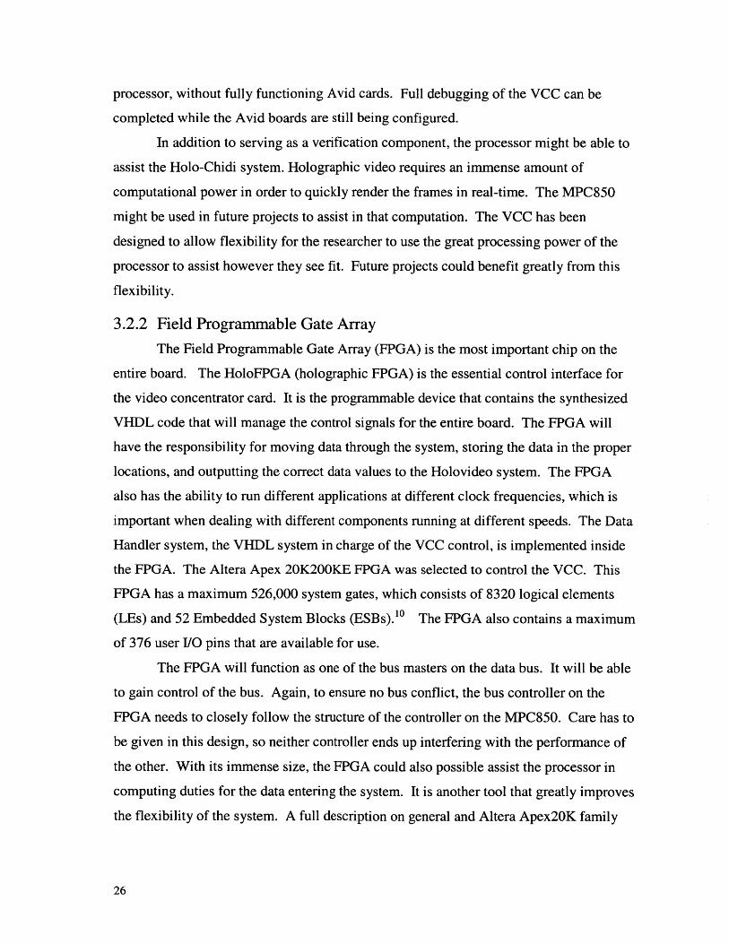
3.2.3 LVDS Interface
The system incorporates a Low Voltage Differential Signaling (LVDS) standard
for point-to-point physical layer interface data transfer. LVDS is a high speed, low
power general purpose interface standard that allows for the ability to transfer data at
high rates. Through the use of differential signal transfer techniques, LVDS technology
delivers the bandwidth necessary for high-resolution displays, while maximizing bit rates.
CMO3/1T OUTPLT3
FED I
Th S038 Al pie VSDslyRcieranftudbyNina
GRN t
A2 8 U
ELJ2
tvti NS.).
Am t s CR (te C. Ias
mxud x at 12 MHz f
(Gbps). It decodes 8 LVDS data streams 48 bits of CMOS/TTL data and 3 control bits.
The LVDS connection will be the main method of communication between the Avid
cards and the VCC. The computed fringe patterns will be passed through the LVDS
connection, to the Display SDRAM and on to the DACs for analog conversion. Three
27

LVDS receivers are required per board, and each will handle two channels of holographic
data.
The computationally intensive holovideo system requires high bandwidth in order
to allow real-time streaming of the holographic frames. The faster the throughput, the
faster the frames become available to the Mark-II Display system. In addition, LVDS
technology is not dependent on a specific power supply, such as +5V. This means there
is an easy migration path to lower supply voltages such as +3.3V while still maintaining
the same signaling levels and performance. This is useful for the Video Concentrator
Card, since the various chips need different voltage levels in order to function. The
LVDS system enables us to power this variety of chips without worrying about the
integrity of the signal. The LVDS system accomplishes high data rates, low power, and
reduced EMI effects by reducing the signal levels.
3.2.4 Digital to Analog Converter
In order for the Mark-II system to function properly, it requires RF analog signals
to drive the AOMs. Since holographic data is in a digital format when is arrives at the
VCC, it will need to be converted into an analog format. Also, the analog signals need to
be powerful enough to drive the holographic display. The Texas Instruments TVP3010
Video Interface Palette is the device being used on the board. This device can
accommodate 64-, 32-, 16-, 8-, and 4-bit pixel buses without any additional circuit
modifications. The device contains three 8-bit digital to analog converters, which are
capable of directly driving a doubly-terminated 75-4 line. The device is also highly
system integrated. It did not require any external buffer logic when connected with the
data bus. External buffers were utilized, only to detach the two data bus paths for the
inputs from one another, in an effort to avoid possible bus contention.
3.2.5 SDRAM
The SDRAMs, or Synchronous DRAMs, are the main storage component of the
VCC. This is where the frames will be stored and made available for output or
manipulation. The Micron MT48LC16M16A2 256 Mb SDRAM was selected for the
system. It contains 4 banks of 4 Megabits (Mbs), each 16 bits deep. This component was
selected for its ease of use, fast writing times, and for its storage locations of 16 bits.
28

Two of these memory chips are enough to handle a 32-bit data bus. Another major
benefit of this SDRAM is its allowance of burst reads and writes. A burst transfer means
that accesses start at a selected location and continue for a programmed number of
locations in a programming sequence.13 The burst lengths of 1, 2, 4, or 8 locations, or
the full page is programmable for the READ or WRITE operations. This allowance for
synchronous burst data transfers at high speeds is essential for efficient data transferring
within the Video Concentrator Card. The quicker data can be stored, the faster it can be
outputted, or made available for possible computational purposes. The SDRAMs are
divided into two sections on the board: main memory and video memory.
3.2.5.1 Main Memory
The Main Memory is a bank of 4 SDRAM's connected to the data and address
buses. These buses are accessible to both the FPGA and the processor. The main
purpose of this memory is to store frames of data that enter the system through the USB
port. Data is stored in the SDRAM, and then it is outputted to the DACs. This SDRAM
is initially used for verification of the VCC system. Eventually, these memory banks can
be used to assist the processor and the FPGA with its processing potential. Frames can
be stored in the main memory, in order to be accessible by these devices for computation
or manipulation. This is another level of flexibility that gives the VCC great potential to
become more than a simple frame buffer.
3.2.5.2 Video Memory
The video memory is also known as the display SDRAM. This section of
memory is responsible for actually storing frames as they enter from either of the input
interfaces. The data is passed on to the DACs for conversion to analog format. There are
12 SDRAMs on the board that make up the display SDRAM. Each channel has two
associated SDRAMs. Two were necessary for the 32-bit streams of data, since the
SDRAM can only store 16-bits at any given location. Each holo-line will store data on
these SDRAMs to allow for error recovery and better streaming of holographic frames
that might be slowed due to intense computation.
29

3.2.6 Flash ROM
The main purpose of the Flash ROM is to contain the boot code for the processor.
The processor will not be able to function unless it is loaded with the proper
programming. The Am29LVO40B is 4 Megabits (512K x 8-Bit), composed of eight 64
Kbyte sectors, that operates at low power levels. 14 Also, any combination of these
sectors can be erased, including the full chip. One problem with the ROM is that it
outputs only 8 bits for any address, even though the rest of the system, including the
processor, runs on a 32-bit bus. So, 4 addresses were required in order to receive one full
command for the MPC850. The Flash ROM has an access time as fast as 60 ns.
3.2.7 Alphanumeric Display
The alphanumeric display is one of the main tools to test the functionality of the
system. It displays data on 4 display modules that can display 5x7 dot matrix characters.
It contains RAM memory to allow displayed data to be stored until over-written by newer
data. The Infineion DLO-1414 alphanumeric display has to ability to output 128 special
ASCII characters. 15 For the purpose of testing, the board only requires the display to
show hexadecimal numbers.
to 19
Display
Rows 0 to 6 , 1 11 13 2 1 0
Row ConCrol Logic dColumns 0
Row Drivers
T
0SC -028e +7ute Timing and Control Logic
RAM Read Logic _Row DecoderD6 ROMD E 7 Bit ASCI I Code Column DataD 4 RAM C 35 Bit
Memory gCharacterD1i Decode
D o 4 X 7 bit 4480 bits
WR WriteAo Address
Ai Decoder
Figure 8: Alphanumeric Display Block Diagram 5
30
Column EnableLatches andColumn Drivers

With this device, the actual state of the system can be viewed. Two of these
displays were used on the board. Using these 8 character displays, any set of signals
could be viewed. As the system operates, the addresses to which the holographic
information is being written can be displayed, or the data that is actually being
transmitted. This flexibility improves the ability to verify the functionality of the board
at a faster pace.
3.3 Implementation
Once these functional blocks were selected for the VCC, they needed to be
acquired and assembled on the board. Upon completion of the assembly, the boards were
then ready to be tested. The initial power up and test of the board proved that it was
running at full power and all of the components were on. Now, the focus of the projected
shifted to the development of the data processing subsystem that would control the
functions of all the hardware.
31

32

Chapter 4: System Control LogicIn order to understand how to design a control system for the VCC board, one
must first understand what designing a system entails. A specific methodology must be
set in order to avoid confusion and allow for a stable design. The tools required for such
a task must be studied and understood to allow the design to function at peak efficiency.
The device on which the design will be placed must be looked at as well. Every device
has its own abilities, which can benefit and also hinder design efficiency.
4.1 General FPGA Overview
The device that we will be using to handle the control design for our board is an
FPGA, or Field Programmable Gate Array. An FPGA is essentially a two-dimensional
array of programmable logic cells. These cells can communicate with one another and
also with 1/0 pins connected to the device. Through the use of routing wires, or
channels, the different programmable elements can communicate with one another in the
device. A programmable, switching network, known as interconnects, are placed in a
grid-like structure made of vertical and horizontal columns. These interconnects can be
enabled or disabled to create logical communication paths between the logical cells. The
channels also connect the logic cells to the 1/0 pins that enable the programmed logic to
interface with the rest of the system.
FPGAs have many desirable qualities that are essential for the efficient operation
of the VCC. Reprogrammability is one of the most important benefits. FPGAs can be
reprogrammed hundreds of times, which is important when debugging a design. If this
option did not exist, it would be impossible to implement a perfect design on the first
attempt. Also, due to the flexible nature of the duties of the FPGA in the VCC,
reprogrammability allows the researchers to experiment with how it is used in the system.
FPGAs are versatile devices. They can handle multiple designs within its logical
structure. In the VCC, the FPGA will need to handle the control logic of the system, but
could also contain some processor functions, if desired. Since all of these abilities fit
within one device, space on the crowded VCC is saved.
33

Though ideal for the VCC, FPGAs do not come without their share of drawbacks.
Timing analysis of an FPGA can prove to be difficult. Signal propagation delays become
a function of the number of cascaded logic cells, the number of programmable
interconnects through which the signal propagates, the technology used to design the
system, fan-out, and 1/0 cell delays.16 If this information cannot be determined, accurate
estimates of system performance and propagation delays will be difficult to ascertain.
Software packages that contain static timing analyzers can assist in determining these
values.
There are many manufacturers of FPGA's. Xilinx, Altera, and Lucent are some
of the more commonly known ones. An Altera device was chosen as the FPGA for the
VCC. Several factors contributed to this choice. Altera devices are inexpensive, relative
to the amount of gates contained on the device. The designers of the VCC have some
experience with Altera products and software packages. This allows design,
implementation, and verification to be completed in a faster time frame. Also, the Altera
chips are incredibly flexible, as they can be implemented to hold standard logic, or to act
as memory, through the use of the Embedded System Blocks (ESBs).
4.2 Altera APEX 20K200E Design
4.2.1 Overview
The APEX 20K200E device, containing 526,000 system gates, is designed with
the Multicore architecture, which combines look-up table (LUT)-based logic, product-
term-based logic and memory into one package. LUT-based logic provides optimized
performance and efficiency for data-path, register-intensive, mathematical, or digital
signal processing designs. Product-term-based logic is optimized for complex
combinatorial paths, such as complex state machines. Applications involving all three
forms of logic can be integrated in the FPGA. Embedded system blocks (ESBs) are used
to implement memory and product-term-based logic, while logical elements (LEs) are
used when implementing LUT-based logic. Table 1 summarizes the features of the
APEX 20K200E.
34

Features Device
APEX 20K200E
Maximum System Gates 526,000
Typical Gates 200,000
LEs 8,320
ESBs 52
Maximum RAM Bits 106,496
Maximum User 1/0 Pins 376
Table 1: APEX 20K200E Device Features"
The signal interconnections, within the device and with the 1/0 pins, are implemented
using the FastTrack Interconnect system. It is a series of fast, row and column routing
channels that run throughout the length and width of the device.' 0 A block diagram
relationship between all these components is shown in Figure 9.
Four-inputWTfordab path andDSP fundkm.
Prcviuct-rmintegrafion Arhkh-speedicwikvibocand
FatTack4tecomet
1mory mo moy I
10ds suppOftPCI, GTL+,SS A-L 0VE,and otherstandadl.
Fleible integra inof embeJddmenoyindudlngCAM, RAM,ROA( FIR andothermenmyfuncions
Figure 9: APEX 20K200E Device Block Diagram"0
Due to the large number of components on the board, an FPGA with enough I/O
pins to connect to all of the control ports of these devices was required. With its 376 user
I/O pins, the APEX 20K200E was ideal for the unique and demanding requirements of
the VCC.
35
ClxkMa mgement Circuby
Ll Ll I IU
The Data Handler data processing system was implemented with the APEX
20K200E. The FPGA has enough gates to not only implement this system, but also to
allow for further research possibilities as other designs can be included in the device.
This FPGA provides the entire board with flexibility necessary in a research
environment.
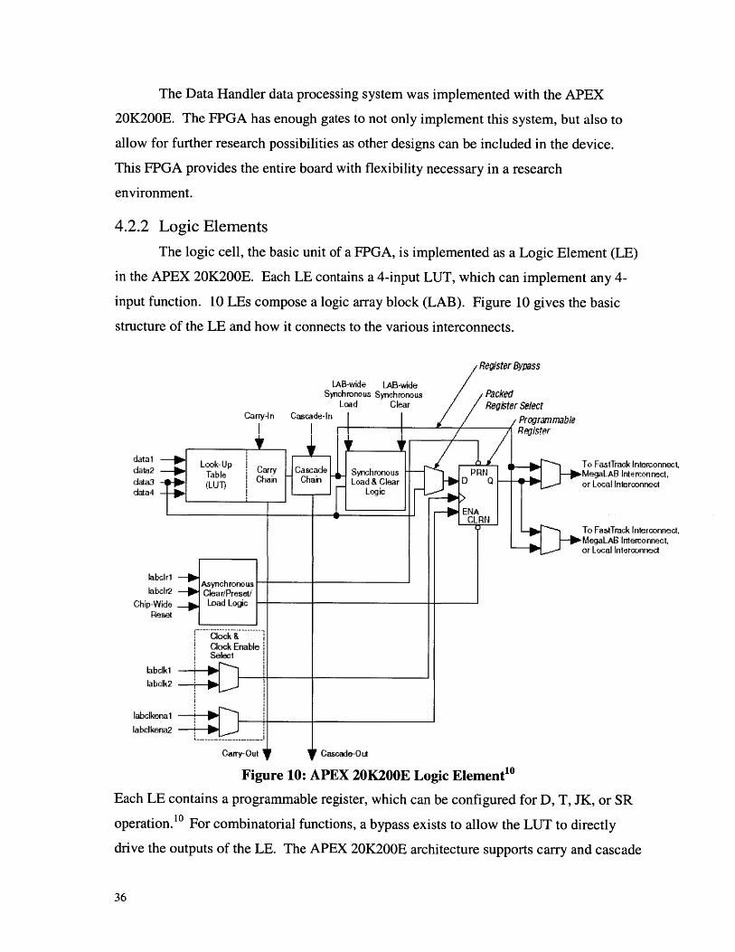
4.2.2 Logic Elements
The logic cell, the basic unit of a FPGA, is implemented as a Logic Element (LE)
in the APEX 20K200E. Each LE contains a 4-input LUT, which can implement any 4-
input function. 10 LEs compose a logic array block (LAB). Figure 10 gives the basic
structure of the LE and how it connects to the various interconnects.
LAB-wide LAB-wideSynchronous Synchronous
Load ClearCarry-in Cascade-In
datal -4 Look-Updata2 -- Table 1 Carry Cascade Synchronousdata3 LUT)LW Chain Chain Load & Clear
data4) Loi
Register Bypass
PackedRegister Select
ProgrammableRmister
PAN ID NQ -
To FastTrack ntMegaLAB Interoor Local lnteroon
- ENACLAN
To FastTrack IntMegaLAB Intercor Local Interoon
labclr1 4AsynchronouslabcIr2 Clear/Preset!
Chip-Wide Load LogicReset
-Clock &Clock EnableSelect
labelkiIabclk2
labclkenal _
labclkena2
Cany-Out Cascade-Out
Figure 10: APEX 20K200E Logic Element 0
Each LE contains a programmable register, which can be configured for D, T, JK, or SR
operation.10 For combinatorial functions, a bypass exists to allow the LUT to directly
drive the outputs of the LE. The APEX 20K200E architecture supports carry and cascade
erconnect,onnect,nect
erconnect,onnect,nect
36

chains. Without using the interconnect resources, adjacent LEs are grouped together.
This feature is useful when designing high-speed adders, counters and wide fan-in
functions.
4.2.3 Embedded System Block
Embedded System Blocks (ESBs) can be used to implement product-term logic
and several memory functions common to logical designs. These functions include
common storage devices, such as context-addressable memory (CAMs), RAMs, dual-port
RAMs, ROMs, and FIFOs. ESBs contain input and output registers that are useful when
implementing memory. The input registers synchronize writes and the output registers
can pipeline designs to improve system performance. ESB memory can be configured in
5 possible sizes: 128x16, 256x8, 512x4, 1024x2, 2048x1. By combining multiple ESBs,
larger memory blocks can be implemented. A block diagram of an ESB module is
located in Figure 11.
37

Dedicated Inputs&Global Signals
Dedicated Clocks I
2or4(2)
~~1
4
4
D 4-j-- ENA
D QENA
~LD~
RAWROM128x 16
250 x 0
Dataln 10242,04,8 x 1
Data Out
Read Address
Yite Address
Read Enable
rite Enable
KriflPulse --
Generalor
to MegaLAB,Im~hatTrack &
Z DO Localr ENA Interconnect
Figure 11: APEX 20K200E ESB in Input/Output Clock Mode'0
In the previous chapter, the use of the FPGA as a flash ROM was mentioned.
ESBs can implement logic functions when programmed with a read-only pattern during
configuration, creating a large LUT. In order to store the boot code for the MPC850, the
FPGA needed to create a 4096x32-bit ROM using the ESBs. The actual implementation
of this ROM will be discussed in Chapter 5.
4.2.4 FastTrack Interconnect
FastTrack Interconnect provides connections between all of the APEX 20K200E
elements. By using a global routing structure, this form of interconnects avoids the
pitfalls that accompany a segmented routing scheme. In a segmented routing scheme,
38
rdM&rs)j -
vffl -
oddrikn -
ixkn -
i::, I i
b D 0 Pop
F
ENA
101 DENA
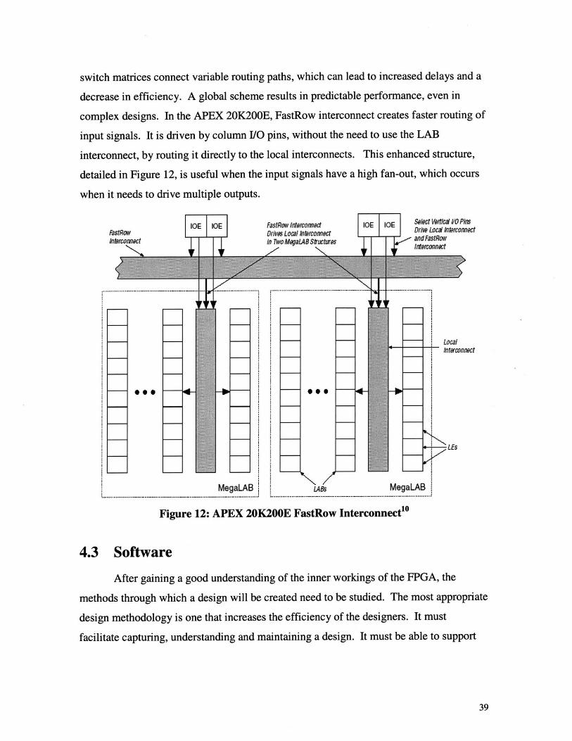
switch matrices connect variable routing paths, which can lead to increased delays and a
decrease in efficiency. A global scheme results in predictable performance, even in
complex designs. In the APEX 20K200E, FastRow interconnect creates faster routing of
input signals. It is driven by column I/O pins, without the need to use the LAB
interconnect, by routing it directly to the local interconnects. This enhanced structure,
detailed in Figure 12, is useful when the input signals have a high fan-out, which occurs
when it needs to drive multiple outputs.
FastRow IntecomectDrives Local IntrconectIn Two MegaLAO Siftures
[oE TOE SelectVelid YO PInand FastRow
~~ii; Intemcnet
*0 0 4-
\J-I II
0*S 4-
Afl
S
MegaLAB LAS MeCLtnD
Figure 12: APEX 20K200E FastRow Interconnect 0
LocalIntMwflflct
4.3 Software
After gaining a good understanding of the inner workings of the FPGA, the
methods through which a design will be created need to be studied. The most appropriate
design methodology is one that increases the efficiency of the designers. It must
facilitate capturing, understanding and maintaining a design. It must be able to support
39
FastRowIntrconect
--- - -----
- ------ -------
n OE OS

complex designs with hierarchy and gate-level to system-level design. It should have the
flexibility to support multiple levels of design description.
There are two hardware description languages (HDLs) that satisfy these digital
design requirements: Verilog and VHDL. Verliog is less verbose than VHDL, but it can
be argued that this is at the expense of language richness and features.1 6 For the purposes
of documentation, synthesis, and simulation for both devices and systems, VHDL is the
best choice for the VCC.
4.3.1 VHDL
VHDL stands for VHSIC (Very High Speed Integrated Circuits) Hardware
Description Language. It has powerful language constructs that can be used to write
efficient code descriptions of complex control logic. The language is highly portable,
meaning synthesized designs can be simulated. Since the language is common in
industry, multiple software packages have the ability to read and synthesize it.
There are some shortcomings associated with VHDL. The control of the
definition of the gate-level implementation of circuits is lost to high-level abstract
concepts. Fortunately this is not a problem that greatly affects most designers. Most
modem synthesis tools give some level of control over the implementation, especially to
make area-efficient versus speed-efficient choices. Also, logic implementations created
by synthesis tools are relatively inefficient. These synthesis tools are designed to be
generic in nature. Compilers use algorithms to decide upon logic implementations,
following standard design methodologies. These implementations might not always be
optimized for a specific design, since the tools are meant to work with all designs and not
a specific one. This problem can be fixed by creating efficient code. Inefficient code can
lead to unneeded, repetitive, or nonoptimal logic.
The Data Handler system is implemented in VHDL. For the purposes of creating
the system level control logic, VHDL was a sufficient language. The designers of the
project were also very familiar with the language and had experience using it to designing
large systems. This led to a more efficient design process, easier debugging, and better
optimizations, leading to a timely completion of the project. Quatus II was the best
package for the development of the Data Handler system, since Altera also built the
FPGA used on the VCC.
40
4.3.2 Quartus II
Altera's Quartus development system offers a single, integrated package that offer
HDL and schematic design entry, compilation, and logic synthesis, full simulation and
worst-case timing analysis. Quartus has support for a wide range of Altera devices,
including the APEX 20K200E. Along with this important quality, it provides several
additional benefits that made it the ideal package to use for the VCC control logic. The
Quartus software supports system level design with block-level editing, workgroup
computing and expanded support for Altera Megafunctions. A megafunction is a pre-
verified HDL netlist files for complex system-level functions and are optimizedfor Altera
device architectures.17 It is a convenient way for a designer to create simple logical
designs, or to view the techniques necessary for taking full advantage of Altera hardware.
Quartus can incrementally recompile designs, which can lead to huge savings in
development time. Any small changes will not require an entire system-wide
recompilation, but will only recompile the module in which the modified code exists.
Quartus also provides full support for VHDL, the chosen HDL for the VCC.
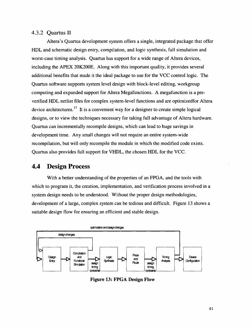
4.4 Design Process
With a better understanding of the properties of an FPGA, and the tools with
which to program it, the creation, implementation, and verification process involved in a
system design needs to be understood. Without the proper design methodologies,
development of a large, complex system can be tedious and difficult. Figure 13 shows a
suitable design flow for ensuring an efficient and stable design.
Figure 13 FPGA Design Fow
41
4.4.1 Design Entry
The first step in developing designs for FPGAs is to formulate a design in a way
that utilizes a particular design environment. This involves specifying the design and
device requirements, deciding on a design methodology, and coding the design. The
device selected for the VCC was the APEX 20K200E. The design was created using a
top-down approach. The top-down approach requires that you divide your design into
functional components, each component having specific inputs and outputs and
performing a particular function.16 A top-level module is created to tie the design
components together. Then the components themselves are designed. The Data Handler
system contains 1 top-level module and 7 components. The design was translated into
logical devices, such as block diagrams, dataflow diagrams, state tables and state
diagrams, which are used to design the general flow of the code. The code for Data
Handler is VHDL-87 compliant. In order to ensure the best design, many of the Altera
examples of VHDL code were used to help design the system code. By doing this, the
code would use the Altera device to its fullest advantage, as their design engineers
created VHDL templates to use as many of the FPGA features as possible.
4.4.2 Compilation and Functional Simulation
After the design is laid out, it was compiled and simulated at the functional level.
This ensures that there are no design flaws with the code, and allows the design to see if
the code functions as expected. This is done with the aid of an EDA software package.
The package contains no information of the target device, or how the design is placed, the
designer must provide the appropriate test vectors for proper simulation. Incorrect
simulation results are typically caused by errors in the source code, or inappropriate test
vectors. Designers targeting the VCC's FPGA use the Altera Design Compiler for
compilation and the Altera ModelSim for functional simulation.
4.4.3 Logic Synthesis
The next stage in the design flow is the logic synthesis. It results in the reduction
of a general design description to a lower-level circuit implementation. It basically
converts a design into a set of equations and netlists. After synthesis, a netlist is created
to show how the components of a design are wired together. Synthesis should be
42

technology specific. By assigning specific timing and area constraints on the synthesis
tool, a designer can attempt to optimize a design to an efficient form. For Data Handler,
Alera's ModelSim was used for logic synthesis.
4.4.4 Place and Route
Once a design is successfully compiled, it needs to be placed onto the logic
device. Propagation delays can depend significantly on routing delays. A good place and
route tool places critical portions of a circuit close together to eliminate routing delays.1 6
A designer must give the proper parameters for place and route, such as the logic
synthesis style, optimizations for speed or area, and device selection. Quartus II was
used to provide place and rout for the VCC FPGA.
4.4.5 Timing Analysis
A successfully placed and routed device must now be simulated according to the
timing constraints of the FPGA. This step not only verifies the functionality of the
design, but also such timing constraints as setup, clock-to-output, and register-to-register
times. A timing simulation allows the designer to see if the design will function, given
the timing information of the target device. If the simulation fails, then the functionality
of the design was violated by the timing requirements. In order to solve these problems,
the design needs to be optimized. Optimization can take place by placing registers in the
critical path delay, a technique known as pipelining. Also, placing timing or placements
constraints on a design before it is synthesized can also shorten delay paths and speed up
the system. Data Handler needed to run at 50 MHz, in order to match the maximum
processing speed of the MPC850.
4.4.6 Device Configuration
After completion of the design, synthesis, optimization, placement and routing,
and successful simulation, the device is ready to be configured and tested in the actual
system. For the VCC, device configuration for the APEX 20K200E is done through the
use of two EPC2 configuration EPROMS. The design, through the use of a Quartus
created .pof file, is burned into the chips, using an Altera MPU programming unit. They
are then placed on the VCC to configure the FPGA upon power up.
43

44

Chapter 5: Data Handler System Implementation
5.1 General Design
Data Handler is the name given to the control logic design for the Video
concentrator Card. Using proper design methodologies, the design was placed in the
Altera APEX 20K200E FPGA. This chapter contains a description of the design flow,
the general coding techniques used throughout the design, and a description of each
component, with verification information.
The Data Handler is meant to be a stable and efficient system that properly
configures the VCC, as well as creating the architecture to allow for flexible use of the
FPGA. The functional scope of the FPGA can change from project to project, but these
changes will be made at the top hierarchy of the existing system. The Data Handler has
several design goals that need to be supported for the VCC to be appropriately
configured:
1) Processor initialization
2) Bidirectional data and address buses
3) Port programming of the alphanumeric display
4) Interfacing with the bus arbiter resident in the processor
5) An optional internal 2048x32-bit ROM
6) Initialization of system SDRAMs
7) SDRAM writing
8) Debug port configuration
These design goals make up the initial version of Data Handler, the main focus of
this chapter.
5.1.1 Top-level Design
At the top level of the system, there are seven components, some of which have
their own set of sub-components. These 7 components are referenced at the top-level
design file. Using the top-down design method, the top-level file was first created and
45

then each subcomponent was created and tested before moving on to the next component.
A basic structure of the Data Handler is included below in Figure 14.
ProcessorBus
ControlSDRAM SDRAMWrite Initialization
AlphanumericSystem /L \---- Data Handler Display
Initialization Top Level Port
Programming
Flash ROM FPGAData Retrival ROM
Figure 14: General Structure of the Data Handler System
This method adopted in Figure 14 allowed for easier verification of the actual
board as each component on the board could be isolated and tested independently. The
FPGA was designed so that it will be used for testing the entire system. Although the
schematic design and actual layout were completely reviewed and verified, any design
flaws that could have occurred during the fabrication might not be detected until the
signal routes started being used by the board components.
The first design of the Data Handler only created a netlist, which set all of the
user-defined pins on the FPGA as inputs. The parameters in the Quartus II allowed some
control for the settings of all the user-specified pins on the chip. If there was no logic
that utilized a pin, then that pin was held at a default value. Inputs were held to high-
impedance, while outputs where held low by default. Since many of the devices on the
board are asserted low, setting all of the pins as outputs would have enabled every device
on the board and led to inadvertently enabling of signals, bus contention and timing
errors. With all of the signals initially specified as inputs, the initial configuration of the
FPGA could be tested, ensuring that the EPC2 configuration device's configuration and
the FPGA itself were functioning properly.
46

Also, since the design of the board was specified before work was begun on the
VHDL code for the FPGA, the pins of the FPGA were pre-specified and routed
throughout the board. This meant that a normal place and route, which places the pins
assignments in the most efficient arrangement depending on the code, could not be left up
to the software. These pins needed to be individually specified and "forced" to the values
assigned during the initial design phase of the system. The designers felt that this would
be the best option for the system, since designing the code before building the board
would have led to an extremely slow development process.
A successful trial run proved that the FPGA and its configuration devices were
functioning according to specifications. The FPGA is currently being clocked at 48
MHz, in order to match the operating frequency of the processor. Design then began on
the actual components that would be instantiated at the top-level design file. For the sake
of modularity each component of the design was separated into individual files and
referenced in the root file. This made the code easier to understand, and ensured that
debugging of individual components could be accomplished with greater efficiency.
5.1.2 Common Designs
VHDL has the ability to allow a designer to create a component and then
instantiate that component as many times as desired in a different file. This eliminates
the repetition of routines in each component. The Data Handler utilizes several basic
logical constructs in multiple places in the design. The Data Handler design is optimized
for the Altera system architecture.
5.1.2.1 Finite State Machine
Finite state machines (FSMs) are commonly used implemented in programmable
logic designs. FSMs are usually generated from state diagrams. State diagrams consist
of the possible states of a system, and transition flows that show how a given state is
entered or exited. These transitions usually occur given the condition of some input
signal. If the input signal does not hold the value given to any of the transitions then the
FSM does not transition out of its current state. Each state holds the value of all the
output signals of the FSM. These outputs are assigned values given the current state.
When the FSM transitions into a new state, the outputs are given the new states values.
Since all HDLs support FSMs, they are an easy way for a designer to specify complex
47
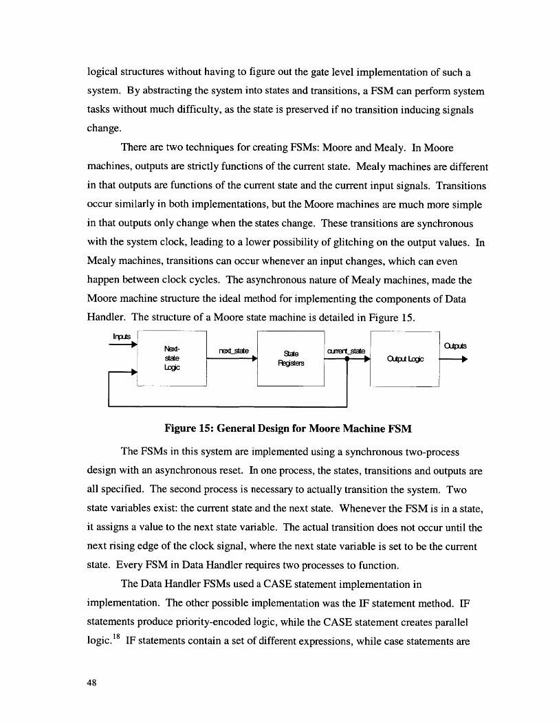
logical structures without having to figure out the gate level implementation of such a
system. By abstracting the system into states and transitions, a FSM can perform system
tasks without much difficulty, as the state is preserved if no transition inducing signals
change.
There are two techniques for creating FSMs: Moore and Mealy. In Moore
machines, outputs are strictly functions of the current state. Mealy machines are different
in that outputs are functions of the current state and the current input signals. Transitions
occur similarly in both implementations, but the Moore machines are much more simple
in that outputs only change when the states change. These transitions are synchronous
with the system clock, leading to a lower possibility of glitching on the output values. In
Mealy machines, transitions can occur whenever an input changes, which can even
happen between clock cycles. The asynchronous nature of Mealy machines, made the
Moore machine structure the ideal method for implementing the components of Data
Handler. The structure of a Moore state machine is detailed in Figure 15.
Net- net_stae sze cnent_statestae -- OuA Lc -LoWC
Figure 15: General Design for Moore Machine FSM
The FSMs in this system are implemented using a synchronous two-process
design with an asynchronous reset. In one process, the states, transitions and outputs are
all specified. The second process is necessary to actually transition the system. Two
state variables exist: the current state and the next state. Whenever the FSM is in a state,
it assigns a value to the next state variable. The actual transition does not occur until the
next rising edge of the clock signal, where the next state variable is set to be the current
state. Every FSM in Data Handler requires two processes to function.
The Data Handler FSMs used a CASE statement implementation in
implementation. The other possible implementation was the IF statement method. IF
statements produce priority-encoded logic, while the CASE statement creates parallel
logic.18 IF statements contain a set of different expressions, while case statements are
48

evaluated against a common controlling expression. CASE statements are used for
complex decoding, which made them ideal for the system design for Data Handler.
Once the state machines have been specified, the designers must determine the
best way to encode the states. There are two types of encoding for a state machine:
sequential and "one-hot" encoding. Every FSM requires registers to store the value of
the state bits. These encoding styles depend on the number of registers that are required
to implement the FSMs, and each has their own advantages and disadvantages.
Sequential encoding involves finding the minimum number of bits necessary to
implement the given number of states in an FSM. This uses a small number of state bits,
but the decoding hardware that will determine the sate of the system can become quite
complex. Sequential encoding can lead to incorrect transitions on large systems with a
high number of states. If more than 1 bit flips between states, then possible glitches and
incorrect state transitions can occur. Designers must enumerate the states so that a
minimum number of bit transitions occur when transitioning between states. One-hot
encoding uses n registers to represent a FSM with n states. Each state has its own
register, and only one holds the value of 1 or gets "hot". Decoding is simplified, since
detection of the register with the 1 is all that is necessary. The complexity required to
decode FSMs with large number of states greatly increases as the number of states
increase, making one-hot encoding the preferred method when an FSM has a large
number of states, and sufficient space exist on the logic device. Typically, FSMs with
fewer than 10 states are encoded sequentially. Anything larger has complex decoding
circuitry, and is better implemented using one-hot encoding. Due to the varying
complexity of the various FSMs in Data Handler, both the sequential and one-hot
encoding styles were used.
5.1.2.2 Counters
Counters are logical devices that increment a given number or signal. While
essentially simple in design, they are complex devices when converted into logical
equations. Counters utilize adders to implement the incrementing. Logical adders are
complex logical structures that get more complex the larger the size of the vector used for
counting. Every use of a '+' in VHDL also creates a new adder, so implementing
efficient counters is important.
49

VHDL does not have a convenient method for delaying signals. If a designer
wants an output to be assigned a specific value, 100 ns after an FSM transitions to a
certain state, there is no direct way to specify this condition. Wait statements, common
structures in software languages, have no meaning in HDLs. During synthesis, these
statements are usually removed. The only way to delay a signal is to create a delay
counter. Delay counters are usually asynchronously clearable, but synchronously
enabled. When the FSM moves into the new state, it sees if the counter holds a specific
value. If that value exists, it executes the corresponding output assignments. If it does
not have that value, the counter will be enabled, and continue to increment by one value
every clock cycle until the counter reaches the desired value. Thus, delay counters are
useful tools to guarantee that a signal will obey the setup and hold times of the devices on
the board. In Data Handler, counters are created as subcomponents and instantiated only
in the components that use them.
5.1.2.3 Bidirectional Signals
Bidirectional signals are very useful for minimizing the amount of space used to
create a board. They essentially have three states: as an input, as an output, and as a
high-impedance (high-Z) state. The high-Z state exists so the signal does not drive a
shared bus at the wrong time, or so bidirectional pins may be driven by off-chip signals.
When designing bidirectional signals, careful consideration needs to be taken to see when
the signal should be in a certain state.
A bidirectional signal in VHDL can be implemented using a two-process system.
Once the signal is declared as a birectional signal in the VHDL entity list, an internal
signal must be declared that is the same size as the 1/0 bidirectional signal. This signal is
used as a temporary storage location for the value of the 1/0 pin. One process ensures
that the signal will keep its previous value or a value driven onto the pins from another
device. The other process enables the signal to be an output, or those outputs are placed
in a high-impedance state otherwise. Together a bidirectional signal can be implemented,
as one state allows the signal to be driven as an input when the output is not enabled, and
as an output in the other case. Data Handler has several bidirectional signals. Not only
the data and address buses are bidrectional, most of the signals that connect the FPGA to
50

the bus controls of the processor, as those signals will be controlled by the MPC850 in
certain occasions and the FPGA in other occasions.
5.1.2.4 Flip-flops
A flip-flop is a set of logic gates that can store the value of the input when
enabled, or hold the previous value when disabled. A flip-flop is useful when designing
logical systems, since they can maintain values of signals. They are used to improve
critical path delays in a system, by placing them along the critical path. A poorly
designed flip-flop can result in extra propagation delays, which can cause violations of
the timing requirements of the device.
Flip-flops are used throughout the components of Data Handler. The main reason
for these flip-flops is to ensure the stability of signals in the system. Without them,
signals tend to glitch when trying to hold their value combinationally, i.e. by constantly
reassigning the same value to the signal every clock cycle. A flip-flop will allow a
temporary signal to remain stable, while it is sent to the output without glitching. Only
appropriate transitions of the signal will be transmitted to the output. In Data Handler,
these flip-flops are implemented with an asynchronous reset and a synchronous load. On
a system wide reset, they will be cleared automatically, but they will only output new
values when they get a load signal.
5.1.2 System Debugging
Once the initial test of the HoloFPGA system was successful, the next stage of
developing Data Handler took place. The VCC has many headers that are assigned to
pins on the FPGA. These pins are meant for debugging purposes, essentially for
verifying any complex system. These signals were available for assigning any value the
designers needed. After the signals were assigned to the values of other signals, a logic
analyzer could be connected to the debug headers for viewing of different signals. In
VHDL, outputs cannot be assigned to more than one value. When it became necessary to
view an output signal on the logic analyzer, the output signal needed to be mapped to a
temporary variable that was then mapped to the debug port. There are occurrences like
this in many of the components of Data Handler, because at times, it was necessary to
view certain signals when debugging the VHDL code in the actual system, to ensure that
51

it was functioning properly. Once the debugging structure was in place, work began on
the many components of the Data Handler.
5.2 System Initialization
The first component of the Data Handler involved initializing the system. This
requires feeding the MPC850 processor a data vector for its configuration register when
the hard reset (/hreset) signal is asserted. The processor, on which resided the bus arbiter,
had to be enabled properly to avoid bus contention. Bus contention occurs when two
different devices are trying to drive the same bus to a value at the same time. When
dealing with a data bus, special care needs to be taken to be sure that only one device is
driving the bus at a time, hence the need for an arbiter.
5.2.1 Design Overview
This design, though relatively small, combined many of the design techniques
discussed in the previous section. The actual initialization occurred within a FSM,
sysini. This FSM contained 4 states: reset, outhold, datain, and dataout. The small
number of states allowed this FSM to be encoded sequentially. The FSM design is
shown in Figure 16.
hreset
hreset ts or ta or cs(o)
hresetSreset out-hold
rom_dataready ts or ta or cs(O)
data_out data-in
rom-datajrdy rom-data-ready
rom-datajrdy
Figure 16: State Diagram for System Initialization
52

When the system is powered on, it is in an unknown state. This is a problem that cannot
be fixed. Therefore it is necessary to reset the entire system once it is powered on, to
ensure the performance of the system.
On a system reset (activated by pressing a push button located on the VCC), the
system will jump into the reset state of sys_ini. The processor needs to be initialized
before it will function after a reset. A 32-bit data vector, specially designated to properly
enable the MPC850, is placed onto the data bus by the FPGA. After the reset is de-
asserted, the FPGA will continue to output the vector until the processor is prepared to
take control of the data bus. Once the processor is ready, it asserts ts, ta, or cs(O) (See
Appendix A for a complete listing of MPC850 bus arbiter signals). At this point the
processor will take control of the data bus, controlling the necessary signals. Therefore,
the FSM enters datain, unaffected by the changes of these signals. In data_in, the data
bus of the FPGA is no longer outputting the initialization vector. These data pins are set
at high-impedance, no longer driving the bus. This prevents bus contention between the
FPGA and the processor. This means that the data bus was declared as a bidirectional
signal. Whenever the data output enable signal (output.en), an internal signal, is high,
the FPGA will output data to the bus. Otherwise, the data pins are set to input. This
means they will hold whatever value the previous had on them, until driven to a new
value. In order to ensure that the no bus contention occurs, the data bus is zeroed (set to
all '0's), before it sets the data pins to high-Z. The main signals that could possibly cause
bus contention, such as the data pins and the output enable where sent through flip-flops,
ensuring stable signals and no bus contention. The FSM remains in this state, until the
FPGA regains control of the bus. The dataout state will be discussed in the "Data
Retrival" section of Chapter 5.5: Flash ROM Implementation.
5.2.2 Timing Analysis
Upon successful compilation, the sysini FSM was tested in the post-synthesis
timing analysis. The FPGA clock was operating at 48 MHz for this simulation and
simulations for all other components. Upon a /hreset assertion, it takes 12.4 ns before the
data bus begins to output the initialization vector for the processor. Once one of the three
signals, ta, ts, or cs(O), is asserted, there is a delay of 26.2 ns before the data output is set
53

to all zeros. This value is held for 22.8 ns, until the data bus changes to an input and
enters the high-impedance state.
5.3 Alphanumeric Display Port Programming
The next component that was created, involved programming the FPGA to
properly access the alphanumeric display. The alphanumeric display is used for
debugging purposes. Larger bus signals could be viewed in hexadecimal format, 0
through F. Using the hexadecimal format, each display displays of 4 bits. Since the
VCC has 8 display characters, 32-bit numbers could be fully displayed.
5.3.1 Design Overview
The alphanumeric display FSM, alphadisplay, utilized an FSM, a delay counter,
and several flip-flops. The display itself has a large library of ascii values it can display,
so it was necessary to create a small table within the FSM in order to have a hexadecimal
display. It takes 7-bits of data to display an item from the alphanumeric ascii table.
4-Bit Number (Binary) Alphanumeric Data 4-Bit Number (Hex)
0000 0110000 0
0001 0110001 1
0010 0110010 2
0011 0110011 3
0100 0110100 4
0101 0110101 5
0110 0110110 6
0111 0110111 7
1000 0111000 8
1001 0111001 9
1010 1000001 A
1011 1000010 B
1100 1000011 C
1101 1000100 D
1110 1000101 E
1111 1000110 F
Unknown 1011000 X
Table 2: Mapping of data, alphanumeric display data, and hexidecimal values 15
54

The FSM consisted of 13 states: start, disO, disi, dis2, dis3, dis4, dis5, dis6, dis7,
datacheck, delay, write, and restorestate. Due to the large number of states, one-hot
encoding was used for this FSM. The FSM design is located in Figure 17.
55

---- dis sel = 1hreset wr-address =10
start
delay_.c
dtcekdelay 0 write restore-state
disO
dis-sel =0wr-address = 0
dis1
dis-sel =0wr-addres .- 01
dis2
dis-s =0wr-ad ess = 1
dis3 dis-se = 0r-add ss = 1
dis._s = 1
dis4 r-add ss = 0
dis-s = 1wr-ad ess - 01
dis5
dis el = 1wr-a ress =1
dis6
dis7
Figure 17: State Diagram for Alphanumeric Display Port Programming
56

Since the system initialization needs to occur before any other FSM begins to function,
the display needed to use signals common to the sysini in order to transition properly.
On a hard reset, the alphadisplay FSM enters the start state. It deactivates the
displays in this state. Once cs(O) or cs(7) (See Appendix A) is asserted, the display enters
the first phase of writing to the diplay, state disO. Since the designers set the value that
will be written to the displays, an input of 32 data bits is required. The actual bits that are
used by the display are specified in the top-level file with the instantiation of the
alphanumeric display component. In the current design, the first 6 displays look at the 24
lower order bits of the address bus. The last two display the 8 highest order bits of the
data bus. Due to the fact that the same alphanumeric display address and data bus are
shared by both displays, each display can only be written to one at a time, while the other
is disabled. Once one display has been written, the next one is activated and written.
From disO, the 4 bits corresponding to that display are selected, by assigning them to a
temporary signal. The FSM enters the datacheck state, which contains a case statement.
This case statement corresponds Table 2 (see above). It matches the data in the temporary
signal to the chart and finds the appropriate data for the alphanumeric display. The FSM
transitions to the delay state. The reason that the data must be delayed before it can be
written to the display has to do with the setup time of the device. This issue will be
discussed in the Timing Analysis section below. After the appropriate delay, the display
enters the write state. In this state, the display write signal, the data, and the display
address are sent to the display. The data value set in disO is finally written to the display.
Once completed, the FSM moves to the restorestate state. The issues that occur with
having only one bus for alphanumeric data and address are dealt with here. An internal
signal is used to select between the two displays (dis-sel). Depending on this signal, the
first or second display is selected. Next, depending on the address that was most recently
written, the next state is selected. When the disO data was written, the alphanumeric
address was "00". Restorestate will send the FSM to the disi state, where the whole
process will occur again, for the next display address. Once the eighth display is written,
the FSM jumps back to the start state, waiting for cs(O) or cs(7) to toggle again.
57

5.3.2 Timing Analysis
This FSM runs slowly compared to the other components. The reason involves
the setup time discussed above. The setup time for the data of the alphanumeric display
is 280 ns.15 This means that the data and address outputs to the display need to be stable
for that amount of time to correctly write. Since each clock cycle is approximately 20 ns
(48 MHz), the delay counter installed in the component must delay the system for at least
14 clock cycles. The delay counter in the alphadisplay FSM stabilizes the signals for 16
clock cycles (exactly 332.9 ns) to ensure that the signals have been stable for at east 280
ns. A four-bit delay counter module was created for use in this component. This delay
occurs for every display digit, resulting in a propagation delay of 2.832 ps until the
display is finished writing. Not until the display has finished writing will the data on the
display be re-written. Due to the slow nature of the display, there is a possibility that data
that should be shown on the display could change several times before the display is
ready to accept new data. This problem cannot be solved without slowing down the
system entirely, so the display will have time to refresh with the system. By setting delay
counters around the system to synchronize the display and the changes in data, this could
be accomplished. At the time of writing this thesis, this method of solution did not seem
necessary, as signals could be fed through the debug ports to the logic analyzer, which
has the ability to see changes in the data bus at the nanosecond level.
5.4 Processor Bus Control
Once the structure to debug Data Handler was in place, the focus shifted to the
arbiter on the processor. Before data could be successfully placed on the data bus,
control needed to be gained from the internal arbiter of the MPC850. Once the FPGA
had the ability to gain control of the bus, it could route data to its data pins without bus
contention occurring on the data bus.
5.4.1 Design Overview
The bus control FSM, bus_ctrl, allows the FPGA to negotiate for control of the
data bus. Busctrl uses an FSM, several flip-flops, and a bidirectional signal. Four states
were used in creating this FSM: reset, bus-request, buscontrol, and busdone. This
FSM was encoded using sequential methods. The state diagram in located in figure 18.
58

hresetstart
outputen
bus-request
ctrldon bg and bb
bg or (bg and bb)
busidone bus-control
ctrldone ctrl_done
ctrldone
Figure 18: State Diagram for Bus Control Module
On a /hreset, the busctrl FSM enters its reset state. The FSM stalls in this state
while the system initialization occurs. Once the output enable signal goes low, meaning
the processor is initialized and ready for operation, the busctrl FSM transitions to the
bus-request state. In this state, the FPGA asserts br (bus request) (see Appendix A) and
waits for a response from the processor. If the processor asserts bg (bus grant), then the
FSM checks to see if bb (bus busy) is asserted. If it is, this means another device
currently has control of the bus. The FSM continues to wait until the bb goes high, where
upon it drives it low and assumes control of the bus. For this reason, bb is declared as a
bidirectional signal, since the FPGA will drive it if it gets control of the bus, but it will be
driven by another device if that device wins control of the bus. The FPGA can read bb
and output to bb depending on the situation. If no device is using the bus when the
FPGA wins control of it, the busctrl FSM switches bb to an output and drives it low.
The FSM moves to the buscontrol state, once control has been won. It will remain in
control of the bus by continuing to assert bb. The FPGA maintains control of the bus
until whichever component of Data Handler is finished using it and sends ctrldone high.
Ctrldone is an internal signal that allows components to interface with the busctrl
59

FSM. If ctrldone is never asserted, then the bus remains in control of the FPGA.
Otherwise, the FSM moves to busdone, where it releases control of the bus. Once
control has been released, the FSM transitions to the busrequest state again, to attempt
to regain control of the bus for the next module.
5.4.2 Timing Analysis
Once the system has finished initializing, the busctrl FSM begins to request
control of the data bus. The propagation delay from outputen to br is 40.3 ns. The FSM
then waits for the bus to be granted to it. If the bus is not busy, then with a bg, it takes
46.4 ns before the bb is asserted. If the bus is busy, then the delay is directly dependent
on the amount of time it takes for the device with control of the bus to complete its
operations, and release the bus.
5.5 Flash ROM Implementation
With the ability to gain control of the data bus, Data Handler's focus could move
to actually transferring data along that bus. Accessing the information in the Flash ROM
became the next part of the project. The purpose of this system was to load the boot code
for the MPC850 from the Flash ROM. Assembler code, meant to run on the processor,
was complied and converted to a set of 32-bit hexadecimal vectors. Dr. Thomas A.
Nwodoh, a researcher in the Spatial Imaging group, developed the boot code for the
processor.
5.5.1 Data Retrieval
Initially, this component was designed to interface with the AM29LVO40B Flash
PROM on the VCC. This chip could only output a data vector of 8 bits, so it required 4
addresses to store one usable 32-bit vector. Due to a bad contact of the pins in the PLCC
socket that houses the Flash ROM, other immediate alternatives were considered to allow
the development of Data Handler and its verification to proceed. A review of the data
sheet for the APEX 20K200E FPGA, reacquainted the designers with the Embedded
System Blocks (ESBs) contained in the FPGA. A ROM of 2048x32-bits could be created
within the FPGA, while using only 61% (65536/106496) of the ESBs bits on the device.
A ROM of this size could fit all of the current boot code. Also, by implementing the
60
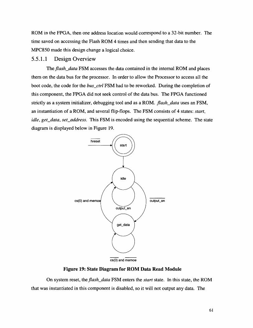
ROM in the FPGA, then one address location would correspond to a 32-bit number. The
time saved on accessing the Flash ROM 4 times and then sending that data to the
MPC850 made this design change a logical choice.
5.5.1.1 Design Overview
The flashdata FSM accesses the data contained in the internal ROM and places
them on the data bus for the processor. In order to allow the Processor to access all the
boot code, the code for the bus_ctrl FSM had to be reworked. During the completion of
this component, the FPGA did not seek control of the data bus. The FPGA functioned
strictly as a system initializer, debugging tool and as a ROM. flash-data uses an FSM,
an instantiation of a ROM, and several flip-flops. The FSM consists of 4 states: start,
idle, get-data, setaddress. This FSM is encoded using the sequential scheme. The state
diagram is displayed below in Figure 19.
hreset1 start
idle
cs(O) and memo outputen
output-en
getdata
cs(O) and memoe
Figure 19: State Diagram for ROM Data Read Module
On system reset, the flashdata FSM enters the start state. In this state, the ROM
that was instantiated in this component is disabled, so it will not output any data. The
61

FSM transitions to the idle state. In the idle state, the ROM remains disabled. When the
system initialization is finished (output-en goes low), the ROM moves into the get-data
state. In get-data, the data in the ROM is accessed by enabling the ROM output. The
MPC850 processor supplies an address and the data for the corresponding ROM location
is returned. The data is fed into a temporary 32-bit signal. When cs(O) and memoe (see
Appendix) both go low, the processor is prepared to receive boot data. The flashdata
FSM sets an internal signal high (rom.datagrdy). This signal is similar to output-en, in
that it is instantiated in the top-level file, so it can be accessible to all the components.
These inter-FSM signals are essential for the smooth integration of all the components
into one system. This point is where the dataout state from the sysini FSM mentioned
above. This state allows the system data bus to output values to the data bus after it has
entered the high-Z state. When it sees romdata-rdy asserted, it starts to drive the value
of the temporary ROM data vector onto the data bus. The MPC850 accesses the data on
the bus, and uses it to run its programs. Once cs(O) and memoe return high, the processor
has successfully received the data and is ready to move to the next address. The FSM
moves back to the idle state, the data pins return to their high-impedance state and the
process continues until the processor has received the last of its boot code.
5.5.1.2 Timing Analysis
Once the system initialization has completed, the flashdata FSM moves into the
get-data state and beings to output the data for the address given by the MPC850. The
data only appears on the data pins when cs(O) and memoe are both asserted low. The
total delay from when theses signals go low until data appears on the data pins is 58.1 ns.
The delay for when an address changes until the data change appears at the output pins is
53.1 ns. These delays demonstrate that accesses to the internal ROM can happen fairly
quickly. In the previous version, using the board Flash ROM, the delay times would
depend on the time it took to read the ROM 4 times, the time it took the processor to
register the data on the data bus, and the delay in takes to receive a new address from the
processor.
62

5.5.2 Creating a ROM
Creating the internal ROM proved to be a fairly simple task. The Megafunctions
of the Altera Quartus II software package contain a VHDL ROM design file that can be
modified to suit the needs of any project, as long as it fits into the device size of the
chosen FPGA. Through the use of the Megafunction Wizard, a ROM was created that
had an 11 -bit address input and a 32-bit data output. The address inputs were clocked
with the system clock of 48MHz. This ensured that only the proper non-glitching values
of the addresses would be read in the ROM. The output changes asynchronously with the
addresses. The synchronicity problem is solved because the data is only being written to
a temporary signal. It is outputted when the romdata-rdy bit goes high, which is a
synchronous transition. So the data bus is always driven synchronously as an output
whenever the romdata-rdy bit is enabled.
5.6 SDRAM Control
The final component that is necessary for Data Handler is the ability to write data
to the SDRAMs, the devices that will serve as the video RAM for the VCC. In order to
achieve this goal, two separate systems need to be put in place: one that initializes the
SDRAM to receive data, and one that actually gets data and writes it to the proper
address in the SDRAM.
5.6.1 SDRAM Initialization
Before the SDRAM devices can be used at all they need to follow a specific
initialization process. Once completed the SDRAM will be able to read out data and
write in new data. The initialization does not need to reoccur unless the system is reset
again. The initialization process is the same for all SDRAMs.
5.6.1.1 Design Overview
The sdramini FSM is designed to run through the one-time initialization process
of the four SDRAM devices that make up the main memory. sdramini uses a FSM, a
delay counter, and various flip-flops for signal stability. The FSM consists of 6 states:
initialize, iniNOP, ini-precharge, ini arefresh, loadmode_reg, and ini_done. These
six states were encoded using sequential techniques. The diagram for the sdramini FSM
is located below in Figure 20.
63

del
delay-cnt
hreset
hrst intaiebusctrl
hreset
ini-done iniNOP
ay_cnt = 11
= 11 loadmodereg ini-precharge
delay-cnt = 10 ini-arefresh
delaycnt = 10
Figure 20: State Diagram for SDRAM Initialization
On a /hreset assertion, the sdramini FSM enters the initialize state. The
SDRAM has 4 control signals, which are used to place the device in one of its many
states.
64
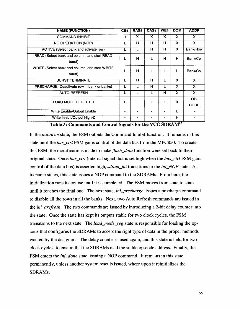
NAME (FUNCTION) CS# RAS# CAS# WE# DoM ADDR
COMMAND INHIBIT H X X X X X
NO OPERATION (NOP) L H H H X X
ACTIVE (Select bank and activate row) L L H H X Bank/Row
READ (Select bank and column, and start READL H L H H Bank/Col
burst)
WRITE (Select bank and column, and start WRITEL H L L L Bank/Col
burst)
BURST TERMINATE L H H L X X
PRECHARGE (Deactivate row in bank or banks) L L H L X X
AUTO REFRESH L L L H X X
OP-LOAD MODE REGISTER L L L L X
CODE
Write Enable/Output Enable - - - - L -
Write Inhibit/Output High-Z - - - - H -
Table 3: Commands and Control Signals for the VCC SDR4 AMl
In the initialize state, the FSM outputs the Command Inhibit function. It remains in this
state until the busctrl FSM gains control of the data bus from the MPC850. To create
this FSM, the modifications made to makeflashkdata function were set back to their
original state. Once bus_ctrl (internal signal that is set high when the busetrl FSM gains
control of the data bus) is asserted high, sdramini transitions to the ini_NOP state. As
its name states, this state issues a NOP command to the SDRAMs. From here, the
initialization runs its course until it is completed. The FSM moves from state to state
until it reaches the final one. The next state, ini_precharge, issues a precharge command
to disable all the rows in all the banks. Next, two Auto Refresh commands are issued in
the iniLarefresh. The two commands are issued by introducing a 2-bit delay counter into
the state. Once the state has kept its outputs stable for two clock cycles, the FSM
transitions to the next state. The loadmode-reg state is responsible for loading the op-
code that configures the SDRAMs to accept the right type of data in the proper methods
wanted by the designers. The delay counter is used again, and this state is held for two
clock cycles, to ensure that the SDRAMs read the stable op-code address. Finally, the
FSM enters the ini_done state, issuing a NOP command. It remains in this state
permanently, unless another system reset is issued, where upon it reinitializes the
SDRAMs.
65

5.6.1.2 Timing Analysis
The SDRAMs can operate at a clock speed of up to 100MHz, so our system
should not run into any timing issues with them. Clocking it at nearly half its maximum
speed (48 MHz) guarantees few timing errors will occur. The load mode register
command is held for 70 ns. The entire initialization of the SDRAMs takes 130ns to
complete.
5.6.2 SDRAM Write
The sdramwr FSM is the most complex FSM in Data Handler currently. It takes
advantage of all the design methodologies described earlier in the chapter. In order to
test the abilities of the SDRAM, the boot code located in the FPGA was the set of test
vectors used. These 32-bit vectors were retrieved from the internal ROM. They were
then sent on to the SDRAMs for writing.
5.6.2.1 Design Overview
The sdramwr FSM functions as a component that can write data to the
SDRAMs, but also manage the control of the data flow through output signals and inter-
FSM signals. flashdata needed to be modified once again. Since the processor was not
supplying addresses for the ROM, an internal address incrementer was implemented.
This module outputs a piece of data for an initial address, and holds that data on the bus
until the SDRAM writing is completed. Then, the incrementer increases the address and
returns the data at the next location. sdramwr consists of a FSM, a delay counter, 3
specialized address incrementers, a bi-directional vector, several signal multiplexers, and
multiple flip-flops. The FSM is made up of 9 states: start, row_ini, get-data, setdata,
write, checklocation, col clear, row-lear, baclear. This FSM was encoded using
sequential encoding. The state diagram for the sdram wr FSMis in Figure 21, located
below.
66

hreset
sdram-ini-donecolhclear rowclear baclear __
hreset
(ba-sel and (ba-sel androw _ad and row-ad and
col-ad col-ad)
(row-ad andcol-ad)
check-location row-ini delay-cnt =11
col-ad
delay-cnt = 11 delay-Qnt = 11
write get-data romn-data-rdy
delaydcnt = 11
romdatarrdy
set-data
Figure 21: State Diagram for SDRAM Write Module
On a system reset, the sdramwr FSM enters its start state. It remains there until
sdramini_done, the internal signal that is asserted once the SDRAM initialization is
completed, where it moves to the rowini state. The reason the command being issued
by this FSM does not affect the initialization of the SDRAMs is that a multiplexer design
was used to switch which addresses appear on the address bus. During the sdramini
FSM, the address bus is driven to the op-code value of loadmode-reg. Once the
sdramwr FSM enters row ini, the address bus outputs the row address for the SDRAM.
The rowini state issues an Active command. This command selects the bank and row in
the SDRAM to activate for eventual writing. For Data Handler, each state checks to see
67

if it should be commanding the first set or second set of Main Memory chips. Since the
SDRAMs have 16-bit data 1/0 pins, two had to be used to get a full 32-bits. rowini is
maintained for 4 clock cycles in order to completely satisfy all the timing constraints of
the device. The next state is get-data. Another inter-FSM signal, sdram-rdy, is asserted
which starts the new flash-data FSM. It gets the data from the current internal address it
is keeping and outputs that vector to the data bus. The data reaches the two data buffer
devices that separate the data bus from the SDRAM data bus. If the romdata-rdy is
asserted, then the ROM data placed on the data bus and the sdramwr FSM transitions to
the setdata state. In this state, the buffers are disabled so no new data coming from the
FPGA can affect the data stored in the buffer. The stable data vector is outputted to the
SDRAM data bus. The FSM enters the write state by selecting the appropriate set of
SDRAMs on which to write. A write command is issued to the SDRAMs, while the data
is still stable on the bus, being driven by the buffer. The address multiplexer selects the
column address. The column address is an incrementer similar to the row address
incrementer. It specifies the appropriate column for the bank that contains the activated
row. Once the write state has been held for 4 clock cycles, the checklocation state
becomes the current state of the FSM. The SDRAMs are issued NOP commands during
this period. In this state, the next location on which to write is selected. If the last
column was written in the previous write, then the row address is incremented and the
FSM jumps to col-clear. If the row address of the previous write was the last row in that
bank, then next bank is selected and the FSM jumps to rowclear. If the bank was the
last bank in that SDRAM, then the next pair of SDRAMs is selected and the FSM jumps
to baclear. If none of these cases are true, then the column address gets incremented
and the FSM moves back to get-data. In colclear, the column address is reset and the
FSM transitions to start. In row-clear, the row address is reset and the FSM transitions
to start. In baclear, the bank address is reset and the FSM transitions to start. Once
both SDRAM pairs have filled up, the system will begin to overwrite the pervious values.
5.6.2.2 Timing Analysis
The sdramwr FSM runs for a long period of time in order to write to every
address of the SDRAM. This time is greater than the simulator in Quartus II can handle,
so no accurate timing information is available for the whole FSM. A row initialization
68

requires 82.3 ns. The delay from entering the get-data state to when data appears on the
actual bus is 44.2 ns. One write cycle takes 61.7 ns. Since bank and SDRAM select
incrementers occur within the rowini state, their propagation delays are equivalent to
those of the row initialization.
5.7 Current System Status
All of the system deign blocks described here are currently functioning, and have
been tested within the VCC. Although the full potential has yet to be realized with the
Data Handler system, the main building blocks for the VCC control logic are firmly in
place. The current code will serve as the basis from which the rest of the system will be
designed.
69

70

Chapter 6: Conclusion
Although the Data Handler system is well underway and a solid foundation has
been established, there are still many components of the design that need to be
implemented before the design is complete.
The Data Handler still cannot take data from the LVDS interface and pass it to the
DACs and out to the Mark-II system. Functionally, this is not a very difficult task.
Obeying all of the timing constraints of the data path could prove difficult to optimize,
but not impossible.
The SDRAM initialization code needs to be applied to the Video SDRAMs.
Since they use different control signals, it's a simple matter of mapping their signals to
the sdramini module. The writing module must also be applied to the Video SDRAMs.
Once these components are in place, the actually testing of the VCC as a
functioning part of the Holo-Chidi system can commence. It is then integrated with the
Avid card and the RF processor of the Mark-II. A back-plane for the large number of
boards will need to be built, so all the boards of Holo-Chidi will have the appropriate
power and interfaces to function properly.
This full verification will prove the most difficult, since the number of variables
that could fail is dependent on several systems. Even if the VCC is working completely,
there is no guarantee that the interface with the Avid card will be completely functioning.
The project is still a year or more away from completion, with two or more designers
working on the project.
6.1 Future Work
Once the Holo-Chidi system is completed and fully functioning, the true research
can begin. Holovideo will need to be retuned to the new devices. New holograms will
need to be rendered to push the limits of the new hardware. The possibility of creating
full motion holographic videos is an incredible challenge in itself.
71

72

Appendix A: MPC850 Bus Arbiter Signals
The MPC850 system bus consists of all signals the interface with the external bus.
In Table 4, the bus signals used by the Data Handler processing system are described.
Signal Active I/O Description
TS Low 0 Asserted by a bus master to indicate the start of a bus cycle thatTransfer transfers data to or from a slave device. Driven by the MPC850 whenStart it owns the external bus. Indicates the start of a transaction on the
external bus.TA Low 0 Indicates that the slave device addressed in the current transactionTransfer accepted data sent by the master (write) or has driven the data busAcknowledge with valid data (read). Driven by the MPC850 when the slave device
is controlled by the on-chip memory controller or PCMCIA interface.CS(O) Low 0 These outputs enable peripheral or memory devices at programmedCS(7) addresses if they are appropriately defined.BR Low I Asserted when a possible master is requesting ownership of the bus.Bus Request Asserting BR when the internal arbiter is enabled indicates that an
external master is requesting the bus.BG Low 0 Asserted when the arbiter of the external bus grants the bus to aBus Grant specific device. When the internal arbiter is enabled, the MPC850
asserts BG to indicate that an external master may assume busmastership and begin a bus transaction.
BB Low I Asserted by a master to show that it owns the bus. As When theBus Busy internal arbiter is enabled, the MPC850 asserts BB to indicate it is bus
master.0 Asserted by a master to show that it owns the bus. As When the
internal arbiter is enabled, the MPC850 samples this signal to getindication of when the external master ended its bus tenure.
Table 4: MPC850 Bus Arbiter Control Signals Descriptions9
73

74

Endnotes
Mark Lucente, "Electronic Holography: Holovideo," MIT Media Lab, SpatialImaging Group, http://www.media.mit.edu/people/Iucente/holo/holovideo.html, 1995.
2 Pierre St.-Hilaire, "Scalable Optical Architectures for Electronic Holography,"Doctor of Philosophy Thesis, Massachusetts Institute of Technology, 1994.
3 M. Lucente, S. A. Benton, P. St.-Hilaire, "Electronic Holography: The Newest,"International Symposium on 3-D Imaging and Holography, Osaka, Japan, 1994.
4 V. M. Bove, J. Watlington, "Cheops: A Reconfigurable Data-Flow System forVideo Processing," MIT Media Lab, 1995.
5 "The Mark-II Holographic Video Display: A Scaled up Design," MIT Media Lab,Spatial Imaging Group, http://www.media.mit.edu/groups/spi/M2.html, 1995.
6 "Chidi: The Flexible Media Processor," MIT Media Lab, Information andEntertainment Group, http://chidi.www.media.mit.edu/projects/chidi/index.html, 1997.
7 "AvidiDS," Avid Technology, Inc., http://www.avid.com/products/avid ds/index.html,2000.
8 "Holo-Chidi: Processing System for Real-Time Holographic VideoComputation," MIT Media Lab, Spatial Imaging Group,http://www.media.mit.edu/-nwodoh/holochidi.html, 1998.
9 "MPC850 Integrated Communications Microprocessor Users's Manual" DataSheet, Motorola, Inc., 2001.
10 "Apex 20K Programmable Logic Device Family," Data Sheet, AlteraCorporation, 2000.
11 "DS90C387A/DS90CF388A Dual Pixel LVDS Display Interface/FPD-Link,"Data Sheet, National Semiconductor Corp., 2000.
12 "TVP3010C, TVP3010M Data Manual: Video Interface Palette," Data Sheet,Texas Instruments, 1997.
13 "256 Mb: x4, x8, x16 SDRAM," Data Sheet, Micron Technology, Inc., 2000.
14 "Am29LV040B," Data Sheet, Advanced Micro Devices, 2000.
15 "DLX1414: Alphanumeric Intelligent Display Devices," Data Sheet, InfinieonTechnologies, 2000.
75

16 Kevin Skahill, "VHDL for Programmable Logic," Addison-Wesley, 1996.
17 "Quartus: Programmable Logic Development System and Software," Data Sheet,Altera Corporation, 1999.
18 "HDL Synthesis for FPGAs: Design Guide," Xilinx Development System, XilinxInc., 1995.
76