A CMOS Visible Image Sensor with Non-Destructive Readout … · 2019-06-10 · A CMOS Visible Image...
8
A CMOS Visible Image Sensor with Non-Destructive Readout Capability Gary R. Sims* a , Gene Atlas c , Eric Christensen b , Roger W. Cover a , Stephen Larson b , Hans J. Meyer a , William V. Schempp a a Spectral Instruments, Inc. 420 N. Bonita Ave., Tucson, AZ USA 85745; b Lunar and Planetary Laboratory, University of Arizona, Tucson, AZ 85721; c ImagerLabs, 1995 S. Myrtle Ave., Monrovia CA 91016 ABSTRACT An experimental camera system equipped with a novel CMOS image sensor suitable for ground-based astronomy that has both destructive and non-destructive readout capability will be described and the performance characteristics including readout noise, dark current, quantum efficiency, will be given. The optimum data collection algorithms to achieve reduced effective readout noise, cosmic ray rejection, and expanded dynamic range will be described. The ability to use destructive readout in select rows to acquire data for telescope guiding while the main part of the sensor is read using non-destructive readout for main image acquisition will be discussed. Keywords: CMOS image sensor, ground-based astronomy, non-destructive readout, up-ramp sampling 1. INTRODUCTION The CCD has been the image sensor of choice for ground-based astronomy for nearly four decades. The combination of low readout noise, low dark current, high quantum efficiency, and large format, large pixel arrays have provided a nearly ideal sensor for most astronomical measurements. CMOS sensors have been developed and employed for space-based systems where radiation tolerance is important and for adaptive optics where high frame rates are necessary. However CMOS sensors are not generally used for routine ground-based astronomy as the principle advantages of CMOS sensor technology have little application for most ground-based astronomy and the availability of appropriate CMOS sensors is limited. In addition, the linear dynamic range of typical CMOS sensors is limited compared to a CCD, which is a marked disadvantage. One report of a large-area CMOS sensor for ground-based astronomy describes the use of a 202mm x 205mm monolithic sensor read at 60 FPS to record meteor tracks at the Schmidt telescope of the University of Tokyo’s Kiso observatory 1 . A custom backside-illuminated CMOS sensor is being developed by E2V for the TAOS-II project of Academia Sinica 2 . This sensor is a three-side buttable array of 1920 x 4608 16 micron square pixels. Read noise is reported to be 3 e- at a frame rate of 2 FPS, and well capacity is 22,000 e- 3,4 . We report here a large-area CMOS image sensor of unique architecture that has potential for application as a sensor for ground-based astronomy. The “DaVinci” sensor produced by ImagerLabs uses a stitched design and has been fabricated as arrays of 2,048 x 2,048 and 4,096 x 4,096 15 micron square pixels using a common mask set. Pixels may be read either destructively (DRO) where charge in the pixel is reset upon readout, or non-destructively (NDRO) where charge is read but not reset. The output is exceptionally linear over a limited charge measurement range. Readout noise is low at moderate to high frame rates. The combination of sensor characteristics combined with an acquisition algorithm similar to that used with infrared sensors overcomes the issue of limited linear charge measurement range and makes it reasonable to consider this as a sensor for routine ground-based astronomy with potential advantages over CCD based sensor such as increased temporal resolution, and the potential to be built as monolithic arrays considerably larger that is available in CCDs. In addition, the ability to mix NDRO or DRO on a line by line basis makes it possible to utilize a portion of the sensor for guiding while acquiring the main image on the remainder of the array. The ability to clear the array quickly using DRO means that an optical shutter is not necessary. *[email protected]; phone 1 520 884-8821; fax 1 520 884-8803; http://www.specinst.com
Transcript of A CMOS Visible Image Sensor with Non-Destructive Readout … · 2019-06-10 · A CMOS Visible Image...

A CMOS Visible Image Sensor with Non-Destructive Readout Capability
Gary R. Sims*a, Gene Atlasc, Eric Christensenb, Roger W. Covera, Stephen Larsonb, Hans J. Meyera, William V. Schemppa
aSpectral Instruments, Inc. 420 N. Bonita Ave., Tucson, AZ USA 85745; bLunar and Planetary Laboratory, University of Arizona, Tucson, AZ 85721; cImagerLabs, 1995 S. Myrtle Ave.,
Monrovia CA 91016
ABSTRACT
An experimental camera system equipped with a novel CMOS image sensor suitable for ground-based astronomy that has both destructive and non-destructive readout capability will be described and the performance characteristics including readout noise, dark current, quantum efficiency, will be given. The optimum data collection algorithms to achieve reduced effective readout noise, cosmic ray rejection, and expanded dynamic range will be described. The ability to use destructive readout in select rows to acquire data for telescope guiding while the main part of the sensor is read using non-destructive readout for main image acquisition will be discussed.
Keywords: CMOS image sensor, ground-based astronomy, non-destructive readout, up-ramp sampling
1. INTRODUCTION The CCD has been the image sensor of choice for ground-based astronomy for nearly four decades. The combination of low readout noise, low dark current, high quantum efficiency, and large format, large pixel arrays have provided a nearly ideal sensor for most astronomical measurements. CMOS sensors have been developed and employed for space-based systems where radiation tolerance is important and for adaptive optics where high frame rates are necessary. However CMOS sensors are not generally used for routine ground-based astronomy as the principle advantages of CMOS sensor technology have little application for most ground-based astronomy and the availability of appropriate CMOS sensors is limited. In addition, the linear dynamic range of typical CMOS sensors is limited compared to a CCD, which is a marked disadvantage.
One report of a large-area CMOS sensor for ground-based astronomy describes the use of a 202mm x 205mm monolithic sensor read at 60 FPS to record meteor tracks at the Schmidt telescope of the University of Tokyo’s Kiso observatory1. A custom backside-illuminated CMOS sensor is being developed by E2V for the TAOS-II project of Academia Sinica2. This sensor is a three-side buttable array of 1920 x 4608 16 micron square pixels. Read noise is reported to be 3 e- at a frame rate of 2 FPS, and well capacity is 22,000 e-3,4.
We report here a large-area CMOS image sensor of unique architecture that has potential for application as a sensor for ground-based astronomy. The “DaVinci” sensor produced by ImagerLabs uses a stitched design and has been fabricated as arrays of 2,048 x 2,048 and 4,096 x 4,096 15 micron square pixels using a common mask set. Pixels may be read either destructively (DRO) where charge in the pixel is reset upon readout, or non-destructively (NDRO) where charge is read but not reset. The output is exceptionally linear over a limited charge measurement range. Readout noise is low at moderate to high frame rates. The combination of sensor characteristics combined with an acquisition algorithm similar to that used with infrared sensors overcomes the issue of limited linear charge measurement range and makes it reasonable to consider this as a sensor for routine ground-based astronomy with potential advantages over CCD based sensor such as increased temporal resolution, and the potential to be built as monolithic arrays considerably larger that is available in CCDs. In addition, the ability to mix NDRO or DRO on a line by line basis makes it possible to utilize a portion of the sensor for guiding while acquiring the main image on the remainder of the array. The ability to clear the array quickly using DRO means that an optical shutter is not necessary.
*[email protected]; phone 1 520 884-8821; fax 1 520 884-8803; http://www.specinst.com

2. SENSOR ARCHITECTURE The DaVinci sensor is based on a novel inverting 3T pixel amplifier in a 15um x 15um pixel with nearly 80% fill factor. The pixel design goals were:
- Very linear response
- 2V full scale voltage output range
- Independence from process parasitic capacitances allowing for very high conversion gain and gain uniformity
- On-chip pixel binning
- Low or no image lag
- Low dark current
- High front illuminated quantum efficiency without resorting to microlenses
The sensor is a stitched device that can be stepped in array sizes from 1K x 1K up to 8K x 8K (the maximum that will fit onto an 8-inch CMOS wafer) subject to sensor yields. 7K x 9K and 6K x 10K maximum formats are also possible.
The 2K x 2K split frame device has 16 analog output ports. Each output port can support pixel rates up to 40Mpix/sec. The sensor operates with a rolling shutter with nearly 100% duty cycle. When operated at full speed the sensor is capable of up to 120 fps.
The sensor can operate with DRO or NDRO, and the mode can be selected independently line by line in real time.
All control clocks are generated by the camera electronics allowing for full external sensor control.
The current sensor is fabricated in a mixed signal low noise 0.35um CMOS process. The starting wafer is a heavily doped bulk silicon wafer with a 5um epitaxial starting layer. An option with 14um thick epitaxial starting wafer is available for improved QE at longer wavelengths. The sensor design is fully compatible with back thinning for improved QE.
Figure 1. 2K x 2K DaVinci sensor mounted on FR-4 carrier board which is then installed in the 1110S camera vacuum chamber. Components above and below the sensor are analog buffers for the sixteen outputs.

3. CAMERA SYSTEM HARDWARE The camera system used to evaluate the DaVinci sensor is based on the Spectral Instruments 1110S CCD camera platform. This is a modern cryogenically cooled multiport camera system commonly used with 2 to 16 port CCDs for ground-based astronomy and other applications with similar requirements. Sensor cooling is achieved with a closed-cycle Joule-Thomson effect refrigerator. The output of the image sensor is digitized to 16 bit precision at 100 MHz sampling rate. The camera was modified to provide the digital timing signals, bias voltages, and precision current sources that the sensor requires. Camera firmware and SI Image system software were modified to accommodate the differences imposed by the CMOS sensor. The camera frame rate is limited to 5.2 frames per second (FPS) due to the limited bandwidth of the fiber optic data link between camera head and computer.
4. SENSOR OPERATION For ground-based astronomy a CCD sensor is typically treated in a manner analogous to photographic film, whereby a shutter is opened to make an exposure, then the shutter closed and the sensor is read. The DaVinci sensor lends itself to a different mode of operation whereby frames are constantly read using either DRO or NDRO, and only the desired frames are captured and analyzed. Constant DROs keep the sensor clear of charge until the camera is commanded to capture a frame sequence. Once the sequence begins, the readout is switched to NDRO and frames are acquired and stored. Both the interval between frames, and the number of frames acquired are parameters controlled by the operator. The first frame read in a sequence is different than subsequent frames. Instead of a NDRO, each line of the first frame is read immediately after the line has been reset (all pixels located on the line are cleared of charge). This first frame contains the offset values for each pixel, including both any fixed pattern offset, and the kTC reset offset for each pixel. This first frame is then subtracted from subsequent frames to remove both fixed pattern offset and kTC noise.
Once a frame sequence has been acquired, the frames may be analyzed using up-the-ramp sampling5 in the same manner as done with IR detector systems. This is used to lower the effective read noise, remove cosmic rays and extend the effective dynamic range of the resulting image frame.
5. SENSOR PERFORMANCE 5.1 Quantum Efficiency
Measured quantum efficiency for the DaVinci sensor is shown in Figure 2. The pixel is approximately 85% open silicon with coatings of SiO2 and Si3N4. Losses in the blue/visible wavelength range are primarily due to optical reflection at the surface. The epitaxy is 5 µm thick, and losses due to transmission become significant in the red/near IR.
Figure 2. Plot of QE for front-illuminated 2K x 2K DaVinci sensor with back-illuminated E2V CCD for comparison. Epi thickness of the DaVinci sensor is approximately 5 µm while that of the CCD is >10 µm.
5.2 Read Noise
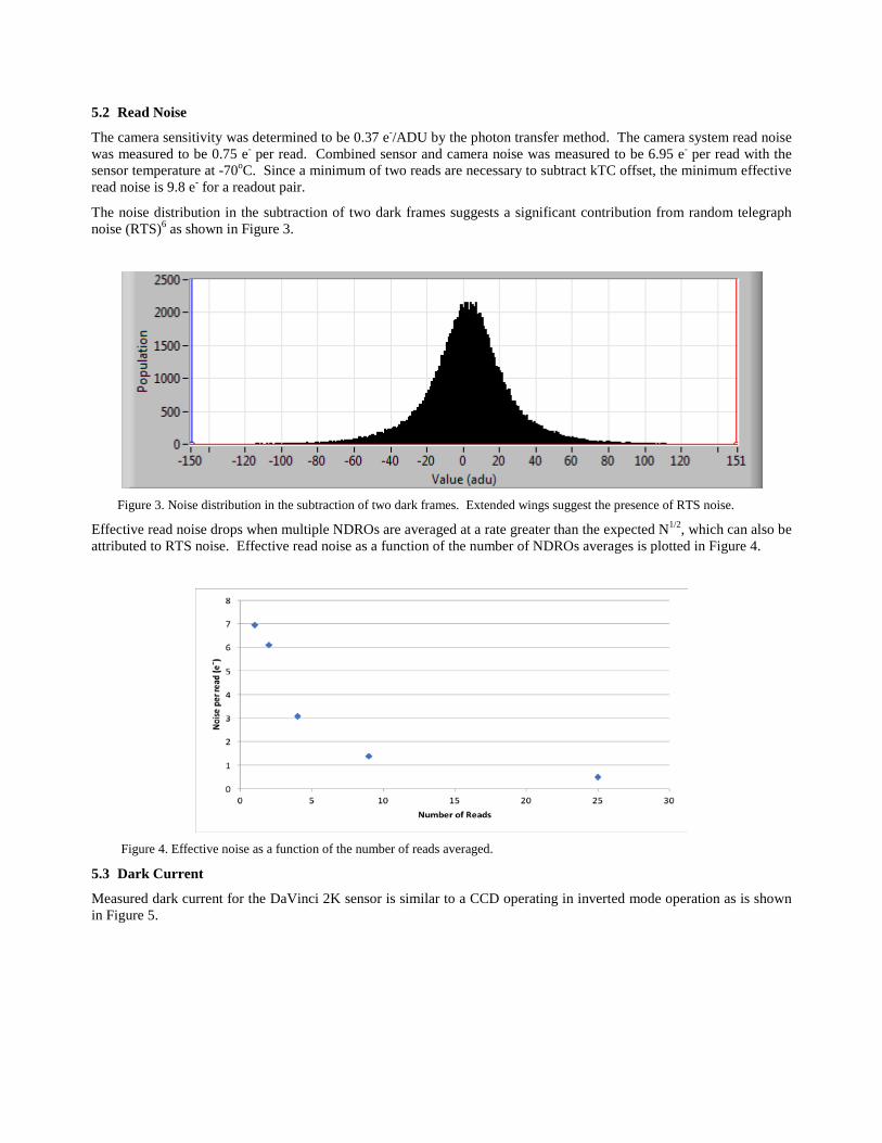
The camera sensitivity was determined to be 0.37 e-/ADU by the photon transfer method. The camera system read noise was measured to be 0.75 e- per read. Combined sensor and camera noise was measured to be 6.95 e- per read with the sensor temperature at -70oC. Since a minimum of two reads are necessary to subtract kTC offset, the minimum effective read noise is 9.8 e- for a readout pair.
The noise distribution in the subtraction of two dark frames suggests a significant contribution from random telegraph noise (RTS)6 as shown in Figure 3.
Figure 3. Noise distribution in the subtraction of two dark frames. Extended wings suggest the presence of RTS noise.
Effective read noise drops when multiple NDROs are averaged at a rate greater than the expected N1/2, which can also be attributed to RTS noise. Effective read noise as a function of the number of NDROs averages is plotted in Figure 4.
Figure 4. Effective noise as a function of the number of reads averaged.
5.3 Dark Current
Measured dark current for the DaVinci 2K sensor is similar to a CCD operating in inverted mode operation as is shown in Figure 5.

Figure 5. Measured dark current as a function of temperature for the DaVinci 2K sensor.
Dark current falls rapidly with temperature. At temperatures below -60oC dark current is difficult to accurately measure as the techniques used for determining CCD dark current, such as the use of binning and overscan regions for reference, do not apply. Some development of novel measurement methods applicable to this sensor need to be developed.
Dark current is generally uniform, but with some evidence of low level luminescence from structures on the periphery of the array on the two sides with row drivers. Figure 6 shows a dark acquisition of 32 minute duration with the sensor cooled to -70oC. 100 NDROs were performed over the 32 minutes, and what is shown is the subtraction of the first image from the last (for kTC and fixed pattern noise subtraction). In this image, there are many spurious events (“cosmic rays”) of which many likely arise from radiation in a glass lens in front of the sensor. Note that in this image there are a few large bright spots that were initiated by a spurious event that slowly grew in size during the remaining acquisition time. This phenomena is not yet understood.
Figure 6. Image showing dark current uniformity in a 32 minute dark exposure. The larger bright spots are due to a phenomena not yet understood. Bright areas on the left and right are evidence of a very low level luminescence from structures at the periphery of the pixel array.

5.4 Charge Measurement Range
The DaVinci sensor is designed to have a 100 µV/e- sensitivity, and a 2V output swing for a 20,000 e- linear operating range. The novel pixel amplifier is designed to be highly linear over this range – similar to the linearity achieved by operational amplifiers. Measuring linearity at this level is difficult, and we have not yet attempted it. We have limited the charge measurement range in our processing to 15,000 e- maximum in order to stay well within the linear measurement range of the sensor.
6. UP-THE-RAMP PROCESSING The utility of up-the-ramp processing is demonstrated in Figure 7, which is an enlargement of an area of the image of Figure 6. On the left is the subtraction of the first image from the last, showing the multitude of spurious events. On the right is the result of up-the-ramp processing of the same complete 100 frame sequence. The effectiveness of spurious event correction is apparent, and in addition the background noise has been reduced by a factor of two. Remaining in the up-the-ramp processed image are residuals from the spurious event correction, and a small number of hot pixels.
Figure 7. Images showing spurious event correction by up-the-ramp processing.
7. INITIAL FIELD TESTS On November 9, 2017 the camera system was mounted on a 40” Steward Observatory telescope located on Mt. Lemmon used by the Catalina Sky Survey for initial evaluation. An enlarged section of one image acquired is shown in Figure 8. This image is compiled from 200 NDROs taken with 0.383 seconds between frames for a total acquisition time of 77 seconds. The 200 images were processed using an up-the-ramp algorithm. No flat field corrections were applied.
The star field has many objects of different brightness. Note that some of the brighter stars have a black dot in the center. This is due to that pixel having charge in excess of the well capacity of the sensor in the first frame. There is some coma in the telescope optics that cause the star images to be slightly misshapen. Note the absence of blooming from the bright stars.
The effective dynamic range in the processed image is in excess of 24 bits.

Figure 8. Star field in Milky Way. 200 NDROs over a 77 second acquisition time. Up-the-ramp processed.
8. DISCUSSION AND CONCLUSIONS
A direct comparison of the DaVinci CMOS sensor to a scientific CCD could lead to the conclusion that the CCD is superior. The CCD has higher quantum efficiency, lower readout noise (per read), much and much higher charge measurement range. A complete understanding of all of the issues, however, may lead to the conclusion that the DaVinci sensor has the potential to be a superior sensor in many applications if further investment in development is made.
8.1 Quantum Efficiency
The Quantum Efficiency of the DaVinci sensor can be increased to levels equivalent to most scientific CCDs by backside illumination plus fabricating on thicker epitaxy silicon. Both are readily achievable. Building the sensor on thicker than 14 µm epitaxy and with high resistivity may be possible, but would likely require more development. An appealing prospect is to fabricate frontside sensors with QE approaching that of backside parts without the impact on yield and subsequent higher cost. This would also require additional development.

8.2 Readout Noise
The readout noise of modern scientific CCDs is approaching 2 e- for slow (100 kHz) pixel rates. Our measurements of the DaVinci sensor at 5 FPS frame rates is appreciably higher, and higher than the manufacturers noise measurements of 2 to 3 e- made at a 40 FPS rate. RTS may account for the difference in noise measurements taken at the two frame rates.
In applications where there is time to make multiple NDROs, the readout noise for the DaVinci sensor is soon not an issue as the effective noise can be lowered below 1 e-. If the device is to be used where there is time for only a single read, such as for guiding, the noise could become an issue. Progress on reducing RTS in CMOS image sensors has been rapid in recent years, and making the DaVinci part using a different more modern process would likely reduce the noise considerably.
8.3 Dark Current
Dark current for the DaVinci sensor is already quite low, and there is little opportunity to reduce it further.
8.4 Charge Measurement Range and Dynamic Range
The single readout intrascene dynamic range for a CMOS image sensor will likely never exceed what is capable for a CCD, but there are other methods to achieve even higher results. The example shown here using multiple NDROs and using up-the-ramp processing is appropriate for the DaVinci sensor. One limitation of this approach is, however, that the signal to noise ratio of the image is still limited by the maximum quantity of charge measured, and it is limited to 15,0001/2 in our use. This limitation could be overcome by the ability to reset the charge in individual pixels either under explicit control, or automatically using a preset threshold.
8.5 Other Considerations
There are several other both immediate and potential benefits to a CMOS sensor with mixed DRO/NDRO capability including:
1) No requirement for an optical shutter,
2) No blooming and spurious event correction allows longer exposure times,
3) Use of DRO in subarrays can be used for on-chip guiding simultaneous with image acquisition using NDROs,
4) Temporal information is always available, whether it is used or not,
5) It is possible to fabricate monolithic arrays much larger than today’s CCDs.
Effective use of the sensor does require computer hardware necessary for processing the image frames, either as a post-acquisition activity or on-the-fly. This is currently routine with IR imaging systems and should not be a obstacle. These advantages are significant and should result in real improvements in image acquisition for ground-based astronomy.
REFERENCES
[1] Watanabe, J. et. al., “Faint meteor observation by large-format CMOS sensor with 1.05-m Kiso Schmidt telescope” Proceedings of the Astronomical Conference held at A.M. University, Poznań, Poland, Aug. 26-30, 2013, Eds.: T.J. Jopek, F.J.M. Rietmeijer, J. Watanabe, I.P. Williams, A.M. University Press, p. 325-328 (2014).
[2] Lehner, M. et. al., “Status of the Transneptunian Automated Occultation Survey (TAOS II)” American Astronomical Society, DPS meeting #49, (2017).
[3] Wang Shiang-Yu et al, “High speed CMOS camera for TAOS-II”, Proc. SPIE 9147 (2014). [4] Jorden, P., Jerram, P., Jordan, D., Pratlong, J., Robbins, M., “e2v CCD and CMOS sensors and systems
designed for astronomical applications”, Proc. SPIE 9915 (2016). [5] Offenberg, J.D., et. al. “Validation of Up-the-Ramp Sampling with Cosmic-Ray Rejection on Infrared
Detectors” Publications of the Astronomical Society of the Pacific, 113:240–254 (2001). [6] J. Janesick, J. Andrews, and T. Elliott, “Fundamental performance differences between CMOS and CCD
imagers: Part I,” Proc. SPIE 6276, (2006).