A CMOS Design Style for Logic Circuit Hardening · PDF fileA CMOS Design Style for Logic...
7
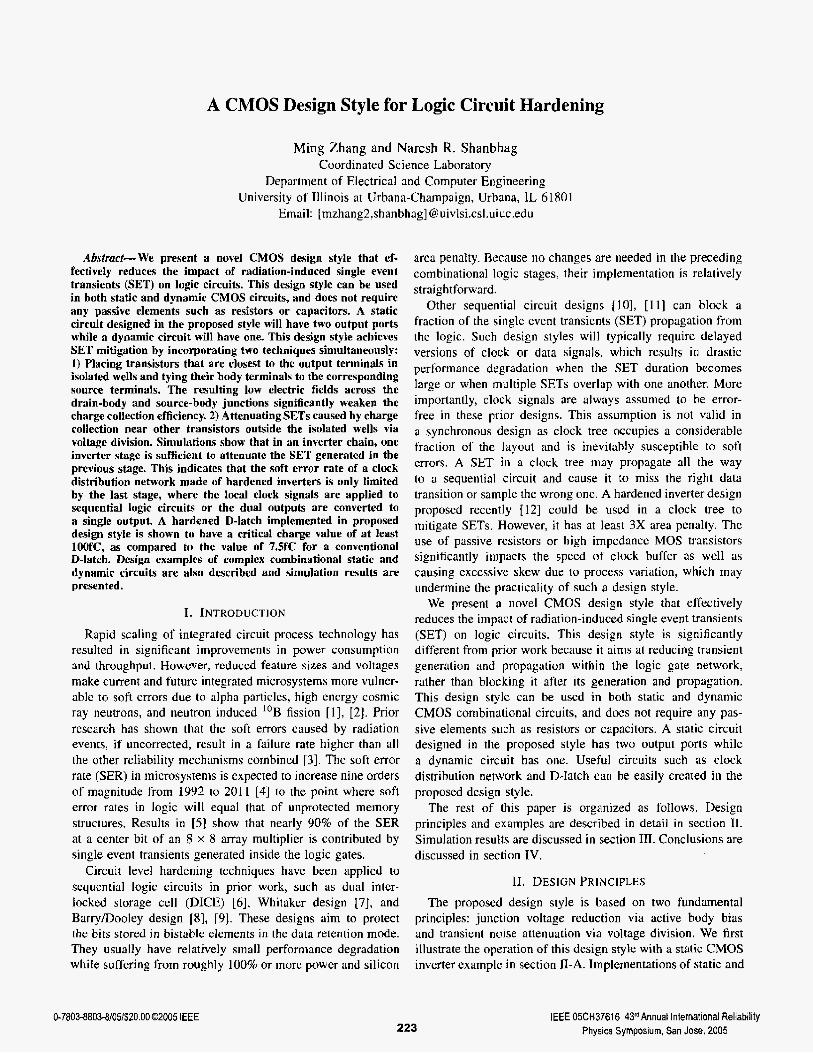
A CMOS Design Style for Logic Circuit Hardening Ming Zhang and Naresh R. Skanbhag Coordinated Science Laboratory Department of Electrical and Computer Engineering University of Illinois at Urbana-Champaign, Urbana, IL 61801 Email: [mzhang2,shanbhag]@uivlsi.csl.uiuc.edu Abstrucf-We present a novel CMOS design style that ef- fectively reduces the impact of radiation-induced singIe event transients (SET) on logic circuits. This design style can be used in both static and dynamic CMOS circuits, and does not require any passive elements such as resistors or capacitors. A static circuit designed in the proposed style will have two output ports while a dynamic circuit will have one. This design style achieves SET mitigation by incorporating two techniques simultaneously: I) Placing transistors that are closcst to the output terminals in isolated wells and tying their body terminals to the corresponding source terminals. The resulting low electric fields across the drain-body and source-body junctions significantly weaken the charge collection efficiency. 2) Attenuating SETs caused by charge collection near other transistors outside the isolated wells via voltage division. Simulations show that in an inverter chain, one inverter stage is sufficient to attenuate the SET generated in the previous stage. This indicates that the soft error rate of a clock distribution network made of hardened inverters is only Iimited by the last stage, where thc local clock signals are applied to sequential logic circuits or the dual outputs are converted to a single output. A hardened D-latch implemented in proposed design style is shown to have a critical charge value of at least lOOfC, as compared to the value of 7SfC for a conventional D-latch. Design examples of complex combinational static and dynamic circuits are also described and simulation results are presented. I. INTRODUCTION Rapid scaling of integrated circuit process technology has resulted in significant improvements in power consumption and throughput. However, reduced feature sizes and voltages make current and future integrated microsystems more vulner- able to soft errors due to alpha particles, high energy cosmic ray neutrons, and neutron induced 'OB fission [I], 121. Prior research has shown that the soft errors caused by radiation events, if uncorrected, result in a failure rate higher than all the other reliability mechanisms combined [3]. The soft error rate (SER) in microsystems is expected to increase nine orders of magnitude from 1992 to 201 1 [4] to the point where soft error rates in logic will equal that of unprotected memory strucmres. Results in [5] show that nearly 90% of the SER at a center bit of an 8 x 8 array multiplier is contributed by single event transients generated inside the logic gates. Circuit level hardening techniques have been applied to sequential logic circuits in prior work, such as dual inter- locked storage cell (DICE) [6], Whitaker design [7], and Bany/Dooley design [8], [9]. These designs aim to protect the bits stored in bistable elements in the data retention mode. They usually have relatively small performance degradation while suffering from roughly 100% or more power and silicon area penalty. Because no changes are needed in the preceding combinational logic stages, their implementation is relatively straightforward, Other sequential circuit designs [IO], [I I] can block a fraction of the single event transients (SET) propagation from the logic. Such design styles will typically require delayed versions of clock or data signals, which results in drastic performance degradation when the SET duration becomes large or when multiple SETs overlap with one another. More importantly, clock signals are always assumed to be error- free in these prior designs. This assumption is not valid in a synchronous design as clock tree occupies a considerable fraction of the layout and is inevitably susceptible to soft errors. A SET in a clock tree may propagate all the way to a sequential circuit and cause it to miss the right data transition or sample the wrong one. A hardened inverter design proposed recently 1121 could be used in a clock tree to mitigate SETS. However, it has at least 3X area penalty. The use of passive resistors or high impedance MOS transistors significantly impacts the speed of clock buffer as well as causing excessive skew due to process variation, which may undermine the practicality of such a design style. We present a novel CMOS design style that effectively reduces the impact of radiation-induced single event transients (SET) on logic circuits. This design style is significantly different from prior work because it aims at reducing transient generation and propagation within the logic gate network, rather than blocking it after its generation and propagation. This design style can be used in both static and dynamic CMOS combinational circuits, and does not require any pas- sive elements such as resistors or capacitors. A static circuit designed in the proposed style has two output ports while a dynamic circuit has one. Useful circuits such as clock distribution network and D-latch can he easily created in the proposed design style. The rest of this paper is organized as follows. Design principles and examples are described in detail in section 11. Simulation results 3re discussed in section 111. Conclusions are discussed in section IV. TI. DESIGN PRINCIPLES The proposed design style is based on two fundamental principles: junction voltage reduction via active body bias and transient noise attenuation via voltage division. We first illustrate the operation of this design style with a static CMOS inverter example in section 11-A. Implementations of static and 0-7803-8803-81051520.00 02005 IEEE 223 IEEE 05CH37616 43m Annual International Reliability Physics Symposium, San Jose, 2005
-
Upload
duongduong -
Category
Documents
-
view
215 -
download
0
Transcript of A CMOS Design Style for Logic Circuit Hardening · PDF fileA CMOS Design Style for Logic...
A CMOS Design Style for Logic Circuit Hardening
Ming Zhang and Naresh R Skanbhag Coordinated Science Laboratory
Department of Electrical and Computer Engineering University of Illinois at Urbana-Champaign Urbana IL 61801
Email [mzhang2shanbhag]uivlsicsluiucedu
Abstrucf-We present a novel CMOS design style that ef- fectively reduces the impact of radiation-induced singIe event transients (SET) on logic circuits This design style can be used in both static and dynamic CMOS circuits and does not require any passive elements such as resistors or capacitors A static circuit designed in the proposed style will have two output ports while a dynamic circuit will have one This design style achieves SET mitigation by incorporating two techniques simultaneously I) Placing transistors that are closcst to the output terminals in isolated wells and tying their body terminals to the corresponding source terminals The resulting low electric fields across the drain-body and source-body junctions significantly weaken the charge collection efficiency 2) Attenuating SETs caused by charge collection near other transistors outside the isolated wells via voltage division Simulations show that in an inverter chain one inverter stage is sufficient to attenuate the SET generated in the previous stage This indicates that the soft error rate of a clock distribution network made of hardened inverters is only Iimited by the last stage where thc local clock signals are applied to sequential logic circuits or the dual outputs are converted to a single output A hardened D-latch implemented in proposed design style is shown to have a critical charge value of at least lOOfC as compared to the value of 7SfC for a conventional D-latch Design examples of complex combinational static and dynamic circuits are also described and simulation results are presented
I INTRODUCTION
Rapid scaling of integrated circuit process technology has resulted in significant improvements in power consumption and throughput However reduced feature sizes and voltages make current and future integrated microsystems more vulner- able to soft errors due to alpha particles high energy cosmic ray neutrons and neutron induced OB fission [ I ] 121 Prior research has shown that the soft errors caused by radiation events if uncorrected result in a failure rate higher than all the other reliability mechanisms combined [3] The soft error rate (SER) in microsystems is expected to increase nine orders of magnitude from 1992 to 201 1 [4] to the point where soft error rates in logic will equal that of unprotected memory strucmres Results in [5] show that nearly 90 of the SER at a center bit of an 8 x 8 array multiplier is contributed by single event transients generated inside the logic gates
Circuit level hardening techniques have been applied to sequential logic circuits in prior work such as dual inter- locked storage cell (DICE) [6] Whitaker design [7] and BanyDooley design [8] [9] These designs aim to protect the bits stored i n bistable elements in the data retention mode They usually have relatively small performance degradation while suffering from roughly 100 or more power and silicon
area penalty Because no changes are needed in the preceding combinational logic stages their implementation is relatively straightforward
Other sequential circuit designs [ IO] [I I ] can block a fraction of the single event transients (SET) propagation from the logic Such design styles will typically require delayed versions of clock or data signals which results in drastic performance degradation when the SET duration becomes large or when multiple SETs overlap with one another More importantly clock signals are always assumed to be error- free in these prior designs This assumption is not valid in a synchronous design as clock tree occupies a considerable fraction of the layout and is inevitably susceptible to soft errors A SET in a clock tree may propagate all the way to a sequential circuit and cause it to miss the right data transition or sample the wrong one A hardened inverter design proposed recently 1121 could be used in a clock tree to mitigate SETS However i t has at least 3X area penalty The use of passive resistors or high impedance MOS transistors significantly impacts the speed of clock buffer as well as causing excessive skew due to process variation which may undermine the practicality of such a design style
We present a novel CMOS design style that effectively reduces the impact of radiation-induced single event transients (SET) on logic circuits This design style is significantly different from prior work because it aims at reducing transient generation and propagation within the logic gate network rather than blocking it after its generation and propagation This design style can be used in both static and dynamic CMOS combinational circuits and does not require any pas- sive elements such as resistors or capacitors A static circuit designed in the proposed style has two output ports while a dynamic circuit has one Useful circuits such as clock distribution network and D-latch can he easily created in the proposed design style
The rest of this paper is organized as follows Design principles and examples are described in detail in section 11 Simulation results 3re discussed in section 111 Conclusions are discussed in section IV
TI DESIGN PRINCIPLES The proposed design style is based on two fundamental
principles junction voltage reduction via active body bias and transient noise attenuation via voltage division We first illustrate the operation of this design style with a static CMOS inverter example in section 11-A Implementations of static and
0-7803-8803-8105152000 02005 IEEE 223
IEEE 05CH37616 43m Annual International Reliability Physics Symposium San Jose 2005
VDD VDD
r T
f- 1 N1
T
GND 6 GND
la) tb)
1NN m (C)
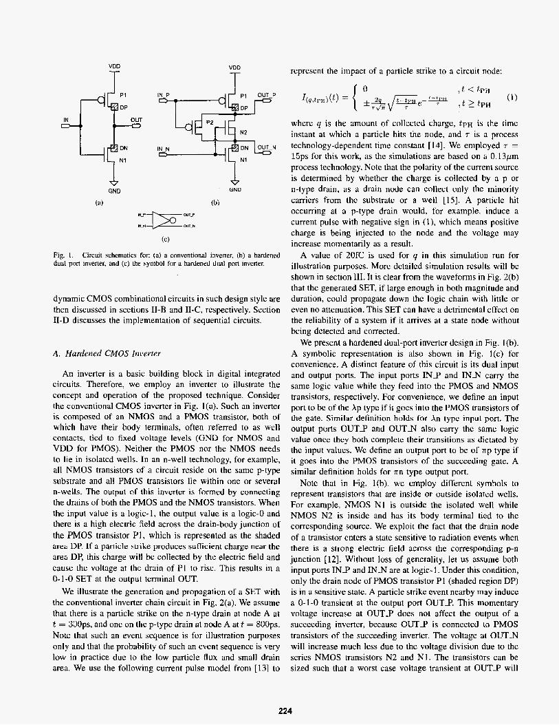
Fig I dual port inverter and (c) the symbol far a hardened dual port inverter
Circuit schematics for (a) a conventional inverter (b) a hardened
dynamic CMOS combinational circuits in such design style are then discussed in sections 11-E3 and 11-C respectively Section 11-D discusses the implementation of sequential circuits
A Hardened CMOS Iiwerter
An inverter is a basic building block in digital integrated circuits Therefore we employ an inverter to illustrate the concept and operation of the proposed technique Consider the conventionill CMOS inverter in Fig 1 (a) Such an inverter is composed of an NhIOS and a PMOS transistor both of which have their body terminals often referred to as well contacts tied to fixed voltage levels (GND for NMOS and VDD for PMOS) Neither the PMOS nor the NMOS needs to lie in isolated wells In an n-well technology for example all NMOS transistors of a circuit reside on the same p-type substrate and all PMOS transistors lie within one or several n-wells The output of this inverter is formed by connecting the drains of bath the PMOS and the NMOS transistors When the input value is a logic-1 the output value is a logic-0 and there is a high electric field across the drain-body junction of the PMOS transistor PI which is represented as the shaded area DP If a particle sti-ike produces sufficient charge near the area DP this charge will be collected by the electric field and cause the voltage at the drain of PI to rise This results in a 0-1-0 SET at the output terminal OUT
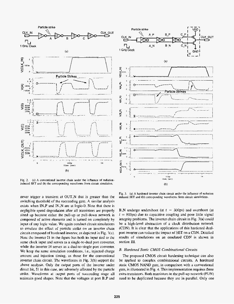
We illustrate the generation and propagation of a SET with the conventional inverter chain circuit in Fig 2(a) We assume that there is a particle strike on the n-type drain at node A at t = 300ps and one on the p-type drain at node A at t = 8OOps Note that such an event sequence is for illustration purposes only and that the probability of such an event sequence is very low in practice due to the low particle flux and small drain area We use the following current pulse model from 1131 to
represent the impact of a particle strike to a circuit node
l o
where q i s the amount of collected charge t p ~ is the time instant at which a particle hits the node and 7 is a process technology-dependent time constant [ 141 We employed T = 15ps for this work as the simulations are based on a 013pm process technology Note that the polarity of the current source is determined by whether the charge is collected by a p or n-type drain as a drain node can collect only the minority carriers from the substrate or a well [ 151 A particle hit occurring at a p-type drain would for example induce a current pulse with negalive sign in ( l ) which means positive charge is being injected to the node and the voltage may increase momentarily as a result
A value of 20fC is used for q in this simulation run for illustration purposes More detailed simulation results will be shown in section 111 It is clear from the waveforms in Fig 2(b) that the generated SET if large enough in both magnitude and duration could propagate down the logic chain with little or even no attenuation This SET can have a detrimental effect on the reliability of a system if it arrives at a state node without being detected and corrected
We present a hardened dual-port inverter design in Fig l(b) A symbolic representation is also shown in Fig l(c) for convenience A distinct feature of this circuit is its dual input and output ports The input ports I N P and I N N carry the same logic value while they feed into the PMOS and NMOS transistors respectively For convenience we define an input port to be of the Xp type if i t goes into the PMOS transistors of the gate Similar definition holds for An type input port The output ports O U T 4 and O U T N also carry the same logic value once they both complete their transitions as dictated by the input values We define an output port to be of ~p type if it goes into the PMOS transistors of the succeeding gate A similar definition holds for m type output port
Note that in Fig I(b) we employ different symbols to represent transistors that are inside or outside isotated wells For example NMOS N1 is outside the isolated well while NMOS N2 is inside and has its body terminal tied to the corresponding source We exploit the fact that the drain node of a transistor enters a state sensitive to radiation events when there is a strong electric field across the corresponding p-n junction [12] Without loss of generality let us assume both input ports I N P and I N N are at logic- I Under this condition only the drain node of PMOS transistor P1 (shaded region DP) is in a sensitive state A particle strike event nearby may induce a 0-1-0 transient at the output port OUTP This momentary voltage increase at O U T 4 does not affect the output of a succeeding inverter because O U T P is connected to PMOS transistors of the succeeding inverter The voltage at OUT-N will increase much less due to the voltage division due to the series NMOS transistors N2 and N1 The transistors can be sized such that a worst case voltage transient at O U T 1 will
224
Particle strike
n
I I J 1 GHz Clock
(a)
Particle strike
I - - __ _ _ _ _ _ _ _ - _ _ _ _ _ _ 7 0 _ ~ ~
- I
1 I
J I
gt ~ ^ - ~ l____l_l_ -~ -^ ~ ~ - I
--- I
I i 1
i t i r i -A
i
j
^ ^ ~ ~ _ _ _ _ _ _ _ ^ ^ ^ _ ^ _ ^~~^~~~___-_II^ ^ ^ ~ ~~
_ I I I i i
a 50Qg lr TFB9 lte)
~ __ _ _ _ I ~
(b)
c SCC n Tiex sec Fig 2
induced SET and (b) the corresponding waveforms from circuit simulation (a) A conventional inverter chain under the influence of radiation-
(b)
never trigger a transient at OUT-N that is greater than the switching threshold of the succeeding gate A similar analysis exists when 1NP and I N N are at logic-0 Note that there is negligible speed degradation after all transistors are properly sized up because either the pull-up or pull-down network is composed of active elements and is turned on completely by input of any logic value We again conduct circuit simulations to emulate the effect of particle strike on an inverter chain circuit composed of hardened inverter as depicted in Fig 3(a) Note the inverter I1 in the figure has both its input tied to the same clock input and serves as a single-to-dual port converter while the inverter I4 serves as a dual-to-single port converter We keep the same simulation conditions ie injected charge amount and injection timing as those for the conventional inverter chain circuit The waveforms i n Fig 3(b) support the above analysis Only the output ports of the inverter under direct hit I1 in this case are adversely affected by the particle strike Waveforms at output ports of succeeding stage all maintain good shapes Note that the voltages at port B-P and
Fig 3 (a) A hardened inverter chain circuit under the influence of radiation induced SET and (b) corresponding waveforms from circuit simulations
B-N undergo undershoot (at t = 300ps) and overshoot (at t = 800ps) due to capacitive coupling and pose little signal integrity problems The inverter chain circuit in Fig 3(a) could be a high-level abstraction of a clock distribution network (CDN) It is clear that the applications of this hardened dual- port inverter can reduce the impact of SET on a CDN Detailed results of simulations on an emulated CDN is shown in section 111
B Hardened Static CMOS Combinatioiial Circuits
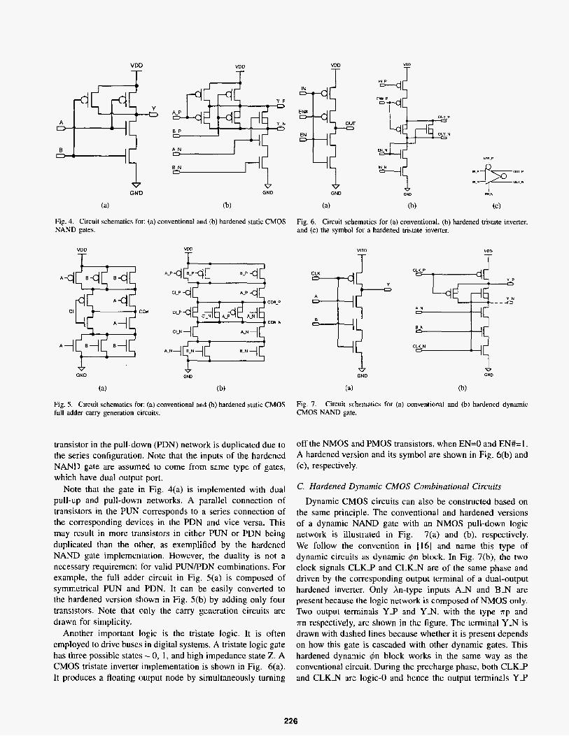
The proposed CMOS circuit hardening technique can also be applied to complex combinational circuits A hardened static CMOS NAND gate in comparison with a conventional gate is illustrated in Fig 4 This implementation requires three extra transistors Both transistors in the pull-up network (PUN) need to be duplicated because they are in parallel Only one
225
i VDD VDD
GND
T
I A N
FWF
GND
t GND E Y GND
(8) (b) (a) (b) (C)
Fig 4 Circuit whematicx for (a) conventional and (b) hardened static CMOS NAND gateb
Fig 6 Circuit schematics for (a) conventional (b) hardened tristate inverter and (c) the symbol for a hardened trixtate invener
M D
T L VDD
T VDD
T
CLK =q N
GND
lsquo7 47 GND
GND
(a) (b) (a) (b)
Fig 5 Circuit schematics for (a) conventional and (b) hardened static CMOS full adder carry generation circuity
Fig 7 CMOS NAND gate
Circuit schematics for (a) conventional and (b) hardened dynamic
transistor in the pull-down (PDN) network is duplicated due to the series configuration Note that the inputs of the hardened NAND gate are assumed to come from same type of gates which have dual output port
Note that the gate in Fig 4(a) is implemented with dual pull-up and pull-down networks A parallel connection of transistors in the PUN corresponds to a series connection of the corresponding devices in the PDN and vice versa This may result in more transistors in either PUN or PDN being duplicated than the other as exemplified by the hardened NAND gate implementation However the duality is not a necessary requirement for valid PUNPDN combinations For example the full adder circuit in Fig S(a) is composed of symmetrical PUN and PDN It can be easily converted to the hardened version shown in Fig S(b) by adding only four transistors Note that only the carry generation circuits are drawn for simplicity
Another important logic is the tristate logic It is often employed to drive buses in digital systems A tristate logic gate has three possible states - 0 1 and high impedance state Z A CMOS tristate inverter implementation is shown in Fig 6(a) It produces a floating output node by simultaneously turning
off the NMOS and PMOS transistors when EN=O and EN= A hardened version and its symbol are shown in Fig 6(b) and (c) respectively
C Hardened Dynamic CMOS Combinationid Circuits
Dynamic CMOS circuits can also be constructed based on the same principle The conventional and hardened versions of a dynamic NAND gate with an NMOS pull-down logic network is illustrated in Fig 7(a) and (b) respectively We follow the convention in 1161 and name this type of dynamic circuits as dynamic $n block In Fig 7(b) the two clock signals C L K P and CLKlV are of the same phase and driven by the corresponding output terminal of a dual-output hardened inverter Only An-type inputs AIJ and B_N are present because the logic network is composed of NMOS only Two output terminals YP and Y N with the type r p and rrn respectively are shown in the figure The terminal YJI is drawn with dashed lines because whether I t is present depends on how this gate is cascaded with other dynamic gates This hardened dynamic n block works in the same way as the conventiona1 circuit During the precharge phase both C L K P and CLKN are logic-0 and hence the output terminals Y P
226
VDO
T
GND
EN 4 Fig 8 gate with keeper
Circuit schematics for (a) conventional and (b) hardened domino
and Y N are charged to logic-1 During the evaluation phase both clock signals become logic-1 and the logic states at the output terminals are retained or modified depending on the input values A dynamic $p block can be similarly derived
The dynamic 4 n and q5p block described above are the basic building blocks of a large design that consists of cascaded dynamic gates We discuss the usage of hardened dynamic circuits for two most important design styles domino logic and np-CMOS (also called zipper CMOS) [ 161
A domino logic module consists of a qh block followed by a static invertcr A keeper transistor is often added to help maintain the logic-1 state at the dynamic node in the evaluation phase if input values are such that the PDN is off Conventional and hardened versions of such a circuit are illustrated in Fig S(a) and (b) respectively A few features need to be emphasized 1 ) the static inverter is hardened and so both the r p and m outputs from the dynamic $m block are needed 2) only one primary output Y of the type 7rn is present because it only needs to be connected to the n-type PDN in the succeeding stage of the domino logic 3) the gate of the keeper PMOS in Fig 8(b) is connected to the 7rp output of the hardened output because this helps reducing the impact of a 1-0-1 SET at the output terminal Y
The np-CMOS design style exploits the duality between n and p blocks This design style is the basis of a popular
L _ _ _ _ - - - _ _ _ _ - _ - - - _ _ I __ - -_______ - -_____ I
Fig 9 Hardened dynamic gales used in the np-CMOS design style
Fig IO Hardened D-latch drawn with part of the clock distribution network
design style called NORA [ I An illustration of hardened np-CMOS logic is shown in Fig 9 Its operation is very similar to that of a conventional np-CMOS logic We omit further discussion of this design style in this paper
To summarize dynamic circuits can also be hardened based on the same principle Only two extra transistors are needed in a dynamic qjn or q5p block because there is always one transistor in series with others in either PUN or PDN
D Hardened CMOS Sequerrtial Circuits
Sequential circuits encompass a large family of designs whose outputs depend on not only the current but also the previous input values Detailed discussion is beyond the scope of this paper We illustrate the application of the proposed design technique in a frequently used D-latch circuit as shown in Fig 10 This design is made to be fully compatible with the dual port nature of the hardened static CMOS circuit Both its inputs (clock and data) and output are dual-ported Note that symbols for hardened inverter (Fig I (c)) and tristate inverter (Fig 6(c)) are used in the circuit schematics
111 RESULTS A N D DISCUSSION To further quantify the performance of proposed circuit
design technique we study in more detail three types of circuits in this section inverter chain D-latch and domino circuits The soft error-tolerance of the hardened circuits are compared with the conventional circuits
We consider two scenarios when simulating the inverter chain circuit
227
TABLE I PARTICLE S T R I K E ON CLOCK TREE
Qcrit for conventional circuits (fC) Qcrjt for hardened gt 100 gt 100 gt 100 circuits (fC)
strike distance P(SE1hit) for conventional
The inverter chain is part of a CDN and is affected by particle strikes We assume that the inverter chain is connected to the clock input of a rising-edge triggered D-flip-flop (DFF) The voltage levels in the inverter chain circuit are set such that the DFF clock input remains zero ie the master latch of the DFF is trans- parent while the slave latch is opaque and retains its state The DFF input is connected to a voltage source whose logic value is opposite to the one stored by DFE A particle strike inside the inverter chain CDN could trigger a SET For a particle strike at a certain distance away from the DFF clock input a minimum amount of charge is required for the SET to propagate to the DFF clock input and cause the DFF sample the value at its input and toggle its original state We define this minimum amount of charge as the critical charge Qcrit corresponding to a specific strike distance which is expressed by the number of inverters A strike distance of zero for example corresponds to a particle strike occurring at the end of the CDN where the clock signal is applied the sequential circuit Simulation results on a 4 inverter chain CDN in both conventional and hardened circuits is shown in Table I It can be observed that the clock tree made of hardened inverter can demonstrate higher degree of soft error-tolerance Note that the Qcrit value is quite close to that of a conventional inverter circuits when the strike distance is zero This i s because a dual-to-single port converter is implemented at the last stage of the inverter chain where DFF clock input is interfaced as previously shown in Fig 3 This node becomes a single point of failure of the inverter chain CDN in this case Taking this into account the SER of an N-inverter chain CDN can be reduced by roughly N x if hardened dual-port inverters are used The inverter chain represents a logic network that pre- cedes the DIT We assume the DITS clock input is connected to a lGHz clock signal The voltage level at the DFF input is set to be either the same as or opposite to the original state of DFF Under the former condition a SET in the inverter chain circuit could have itself latched by the DFF and hence upset the correct state of DIT Under the latter condition a SET could prevent the correct input value from being latched by the DFF and hence the wrong state stays in the DFF We use a previously proposed soft error rate analysis (SERA) framework [5] to study the conditional probability of soft errors given a particle slrike at a specific location
3 j 2 1 1 0 DFF stores 0 0049 0047 0055 0066
circuit5
P(SE1hit) for DFF stores 1 0026 00B 0030 0068 DFF stores 0 0 0 0 0056 I hampdened circuhs
strike distance P(SE1hit) for conventional
3 2 1 I 0 DFF stores 0 0042 0044 0016 0078
circuits
P(SE1lrit) for hardened circuit5 I
- 0065 0063
DFF storex 0 0 0 0 0072
The conditional probability P(SE1hit) terms are shown for both conditions in Tables 11 and HI respectively Again the hardened circuits can tolerate SETS generated anywhere except at the last inverter stage where the dual port is converted to a single pon
Note that in the above simulations we assumed a con- ventional DFF is employed whose data and clock inputs are both single ported This is fundamentally the reason for the existence of a single point of failure where the inverter chain circuit (playing the role of either a CDN or a logic network) interfaces the DFF If a dual ported DFF constructed by cascading hardened dual-port D-latch (shown in Fig 10) is employed together with dual-ported CDN and logic network then the single point of failure caused by dual to single port conversion would disappear The SER of the whole system could improve dramatically as a result
We also simulated the critical charge Qcrit for a D latch composed of conventional and hardened inverters The Qcrit for a conventional D-latch is 75fC while the Qcrit for a hardened one is greater than IOOfC To achieve the same performance (D-to-Q delay) the total transistor width of the hardened D-latch is about 22 times that of the conventional D-latch It is noteworthy that the actual layout overhead of the proposed hardened D-latch may be a little higher due to the extra areas occupied by the isolated wells Detailed study on layout penalty has not been done in this work
Tables IV and V show the simulation results for con- ventional and hardened domino circuits respectively Note that we employ a criterion different from the one used for inverter chain circuits to obtain critical charge values We attach a nominal load to the output of the domino circuit The minimum amount of charge causing the voltage level at
228
TABLE IV
PARTlCLE STRIKE IN CONVENTIONAL DOMINO CIRCUIT
strike location X X Y Y and polarity (1 - 0) ( 0 - 1) (1 + 0) ( 0 - 1) Qcrit (fc) 3 S 2 -1 6S
[6] T Calin M Nicolaidis and R Velazco rdquoUpzet hardened memory design for submicron CMOS technolowrsquo iEeuroE Transacrions on Miclear
[7] M N Liu and S Whitaker ldquoLow power SEU immune CMOS memory circuitsrdquo IEEE Tldquoaciioris on Nuclear Science vol 39 pp 1679- 1684 Dec 1992
strike location and polarity Qcrit (fc)
SETs but the improvement is not as significant as that for
conventional and hardened domino circuits is down-sized for
the atmospheric neutron soft error raterdquo IEEE Transacfioamp on Niiclear Science vol 47 no 6 pp 25862591 December 2000
PhD dissertation LinkopinE University 2000
O-I-0 SETS This is because the keeper in both the [Is] p Hazucha ldquoBackground radiation and errors in CMOS circuitsrsquo
X_N x -P Y Y Y single event upsets from combinational logicrdquo 7th NASA Syrposiwn or1 (1 - 0 ) (0 - 1) (1 -0) ( 0 + 1) VLSI design 1998 8 gt 100 6 4s [ I I ] D G Mavis and P Eaton ldquoSoft error rate mitigation techniques for
performance and hence do not provide sufficient strength to [I61 J M Rabsey Digital Integrited Circuiis Prentice Hall 1996
contend with the 1-0- I SET
Iv CONCLUSIONS
We presented a novel CMOS design style that effectively reduces the impact of radiation-induced single event transients (SET) on logic circuits This design style can be used in both static and dynamic CMOS circuits Simulations show that in an inverter chain one inverter stage is sufficient to attenuate the SET generated in the previous stage A hardened D-latch implemented in the proposed design style is shown to have a critical charge value of at least IOOfC as compared to the value of 75fC for a conventional D-latch Hardened dynamic circuits also demonstrate soft error tolerance improvement over conventional dynamic circuits Future work may include further evaluation and optimization of the proposed design technique based on post-layout data and full integration of dual port combinational and sequential logic circuits on a larger system
V ACKNOWLEDGMENTS This work was supported by the MARCO-sponsored Gigas-
cale Systems Research Center
REFERENCES [ t ] ldquolntemational Technology Roadmap for Semiconductors 2003rdquo
lirippriWic iirs net [Z] R C Baumann ldquoSoh errors in advanced semiconductor devices-part I
the three radiation sourcesrdquo IEEE Trmrsacriuns on Device and Marerials Reliability vol 1 pp17-22 March 2001
[3] R Baumann ldquoThe impact of technology scaling o n soft error rate performance and limts to the efficacy of error correctionrdquo Proceedings of IEEE Inreniariunal Elecirori Devices Meeting pp 329-332 2002
[J] P Shivakumar et al ldquoModeling the effect of technology trend on the soft error rate of combinational logicrdquo Proceedings of Iniemariunul Conference on Dependable Sysremr arid Network pp 389-398 2002
[SI M Zhang and N R Shanbhag lsquoA soft error rate analysis (SERA) methodologyrdquo Proceedings of Internariottol Conference on Computer Aided Design pp 11 1-1 18 2004
229
VDD VDD
r T
f- 1 N1
T
GND 6 GND
la) tb)
1NN m (C)
Fig I dual port inverter and (c) the symbol far a hardened dual port inverter
Circuit schematics for (a) a conventional inverter (b) a hardened
dynamic CMOS combinational circuits in such design style are then discussed in sections 11-E3 and 11-C respectively Section 11-D discusses the implementation of sequential circuits
A Hardened CMOS Iiwerter
An inverter is a basic building block in digital integrated circuits Therefore we employ an inverter to illustrate the concept and operation of the proposed technique Consider the conventionill CMOS inverter in Fig 1 (a) Such an inverter is composed of an NhIOS and a PMOS transistor both of which have their body terminals often referred to as well contacts tied to fixed voltage levels (GND for NMOS and VDD for PMOS) Neither the PMOS nor the NMOS needs to lie in isolated wells In an n-well technology for example all NMOS transistors of a circuit reside on the same p-type substrate and all PMOS transistors lie within one or several n-wells The output of this inverter is formed by connecting the drains of bath the PMOS and the NMOS transistors When the input value is a logic-1 the output value is a logic-0 and there is a high electric field across the drain-body junction of the PMOS transistor PI which is represented as the shaded area DP If a particle sti-ike produces sufficient charge near the area DP this charge will be collected by the electric field and cause the voltage at the drain of PI to rise This results in a 0-1-0 SET at the output terminal OUT
We illustrate the generation and propagation of a SET with the conventional inverter chain circuit in Fig 2(a) We assume that there is a particle strike on the n-type drain at node A at t = 300ps and one on the p-type drain at node A at t = 8OOps Note that such an event sequence is for illustration purposes only and that the probability of such an event sequence is very low in practice due to the low particle flux and small drain area We use the following current pulse model from 1131 to
represent the impact of a particle strike to a circuit node
l o
where q i s the amount of collected charge t p ~ is the time instant at which a particle hits the node and 7 is a process technology-dependent time constant [ 141 We employed T = 15ps for this work as the simulations are based on a 013pm process technology Note that the polarity of the current source is determined by whether the charge is collected by a p or n-type drain as a drain node can collect only the minority carriers from the substrate or a well [ 151 A particle hit occurring at a p-type drain would for example induce a current pulse with negalive sign in ( l ) which means positive charge is being injected to the node and the voltage may increase momentarily as a result
A value of 20fC is used for q in this simulation run for illustration purposes More detailed simulation results will be shown in section 111 It is clear from the waveforms in Fig 2(b) that the generated SET if large enough in both magnitude and duration could propagate down the logic chain with little or even no attenuation This SET can have a detrimental effect on the reliability of a system if it arrives at a state node without being detected and corrected
We present a hardened dual-port inverter design in Fig l(b) A symbolic representation is also shown in Fig l(c) for convenience A distinct feature of this circuit is its dual input and output ports The input ports I N P and I N N carry the same logic value while they feed into the PMOS and NMOS transistors respectively For convenience we define an input port to be of the Xp type if i t goes into the PMOS transistors of the gate Similar definition holds for An type input port The output ports O U T 4 and O U T N also carry the same logic value once they both complete their transitions as dictated by the input values We define an output port to be of ~p type if it goes into the PMOS transistors of the succeeding gate A similar definition holds for m type output port
Note that in Fig I(b) we employ different symbols to represent transistors that are inside or outside isotated wells For example NMOS N1 is outside the isolated well while NMOS N2 is inside and has its body terminal tied to the corresponding source We exploit the fact that the drain node of a transistor enters a state sensitive to radiation events when there is a strong electric field across the corresponding p-n junction [12] Without loss of generality let us assume both input ports I N P and I N N are at logic- I Under this condition only the drain node of PMOS transistor P1 (shaded region DP) is in a sensitive state A particle strike event nearby may induce a 0-1-0 transient at the output port OUTP This momentary voltage increase at O U T 4 does not affect the output of a succeeding inverter because O U T P is connected to PMOS transistors of the succeeding inverter The voltage at OUT-N will increase much less due to the voltage division due to the series NMOS transistors N2 and N1 The transistors can be sized such that a worst case voltage transient at O U T 1 will
224
Particle strike
n
I I J 1 GHz Clock
(a)
Particle strike
I - - __ _ _ _ _ _ _ _ - _ _ _ _ _ _ 7 0 _ ~ ~
- I
1 I
J I
gt ~ ^ - ~ l____l_l_ -~ -^ ~ ~ - I
--- I
I i 1
i t i r i -A
i
j
^ ^ ~ ~ _ _ _ _ _ _ _ ^ ^ ^ _ ^ _ ^~~^~~~___-_II^ ^ ^ ~ ~~
_ I I I i i
a 50Qg lr TFB9 lte)
~ __ _ _ _ I ~
(b)
c SCC n Tiex sec Fig 2
induced SET and (b) the corresponding waveforms from circuit simulation (a) A conventional inverter chain under the influence of radiation-
(b)
never trigger a transient at OUT-N that is greater than the switching threshold of the succeeding gate A similar analysis exists when 1NP and I N N are at logic-0 Note that there is negligible speed degradation after all transistors are properly sized up because either the pull-up or pull-down network is composed of active elements and is turned on completely by input of any logic value We again conduct circuit simulations to emulate the effect of particle strike on an inverter chain circuit composed of hardened inverter as depicted in Fig 3(a) Note the inverter I1 in the figure has both its input tied to the same clock input and serves as a single-to-dual port converter while the inverter I4 serves as a dual-to-single port converter We keep the same simulation conditions ie injected charge amount and injection timing as those for the conventional inverter chain circuit The waveforms i n Fig 3(b) support the above analysis Only the output ports of the inverter under direct hit I1 in this case are adversely affected by the particle strike Waveforms at output ports of succeeding stage all maintain good shapes Note that the voltages at port B-P and
Fig 3 (a) A hardened inverter chain circuit under the influence of radiation induced SET and (b) corresponding waveforms from circuit simulations
B-N undergo undershoot (at t = 300ps) and overshoot (at t = 800ps) due to capacitive coupling and pose little signal integrity problems The inverter chain circuit in Fig 3(a) could be a high-level abstraction of a clock distribution network (CDN) It is clear that the applications of this hardened dual- port inverter can reduce the impact of SET on a CDN Detailed results of simulations on an emulated CDN is shown in section 111
B Hardened Static CMOS Combinatioiial Circuits
The proposed CMOS circuit hardening technique can also be applied to complex combinational circuits A hardened static CMOS NAND gate in comparison with a conventional gate is illustrated in Fig 4 This implementation requires three extra transistors Both transistors in the pull-up network (PUN) need to be duplicated because they are in parallel Only one
225
i VDD VDD
GND
T
I A N
FWF
GND
t GND E Y GND
(8) (b) (a) (b) (C)
Fig 4 Circuit whematicx for (a) conventional and (b) hardened static CMOS NAND gateb
Fig 6 Circuit schematics for (a) conventional (b) hardened tristate inverter and (c) the symbol for a hardened trixtate invener
M D
T L VDD
T VDD
T
CLK =q N
GND
lsquo7 47 GND
GND
(a) (b) (a) (b)
Fig 5 Circuit schematics for (a) conventional and (b) hardened static CMOS full adder carry generation circuity
Fig 7 CMOS NAND gate
Circuit schematics for (a) conventional and (b) hardened dynamic
transistor in the pull-down (PDN) network is duplicated due to the series configuration Note that the inputs of the hardened NAND gate are assumed to come from same type of gates which have dual output port
Note that the gate in Fig 4(a) is implemented with dual pull-up and pull-down networks A parallel connection of transistors in the PUN corresponds to a series connection of the corresponding devices in the PDN and vice versa This may result in more transistors in either PUN or PDN being duplicated than the other as exemplified by the hardened NAND gate implementation However the duality is not a necessary requirement for valid PUNPDN combinations For example the full adder circuit in Fig S(a) is composed of symmetrical PUN and PDN It can be easily converted to the hardened version shown in Fig S(b) by adding only four transistors Note that only the carry generation circuits are drawn for simplicity
Another important logic is the tristate logic It is often employed to drive buses in digital systems A tristate logic gate has three possible states - 0 1 and high impedance state Z A CMOS tristate inverter implementation is shown in Fig 6(a) It produces a floating output node by simultaneously turning
off the NMOS and PMOS transistors when EN=O and EN= A hardened version and its symbol are shown in Fig 6(b) and (c) respectively
C Hardened Dynamic CMOS Combinationid Circuits
Dynamic CMOS circuits can also be constructed based on the same principle The conventional and hardened versions of a dynamic NAND gate with an NMOS pull-down logic network is illustrated in Fig 7(a) and (b) respectively We follow the convention in 1161 and name this type of dynamic circuits as dynamic $n block In Fig 7(b) the two clock signals C L K P and CLKlV are of the same phase and driven by the corresponding output terminal of a dual-output hardened inverter Only An-type inputs AIJ and B_N are present because the logic network is composed of NMOS only Two output terminals YP and Y N with the type r p and rrn respectively are shown in the figure The terminal YJI is drawn with dashed lines because whether I t is present depends on how this gate is cascaded with other dynamic gates This hardened dynamic n block works in the same way as the conventiona1 circuit During the precharge phase both C L K P and CLKN are logic-0 and hence the output terminals Y P
226
VDO
T
GND
EN 4 Fig 8 gate with keeper
Circuit schematics for (a) conventional and (b) hardened domino
and Y N are charged to logic-1 During the evaluation phase both clock signals become logic-1 and the logic states at the output terminals are retained or modified depending on the input values A dynamic $p block can be similarly derived
The dynamic 4 n and q5p block described above are the basic building blocks of a large design that consists of cascaded dynamic gates We discuss the usage of hardened dynamic circuits for two most important design styles domino logic and np-CMOS (also called zipper CMOS) [ 161
A domino logic module consists of a qh block followed by a static invertcr A keeper transistor is often added to help maintain the logic-1 state at the dynamic node in the evaluation phase if input values are such that the PDN is off Conventional and hardened versions of such a circuit are illustrated in Fig S(a) and (b) respectively A few features need to be emphasized 1 ) the static inverter is hardened and so both the r p and m outputs from the dynamic $m block are needed 2) only one primary output Y of the type 7rn is present because it only needs to be connected to the n-type PDN in the succeeding stage of the domino logic 3) the gate of the keeper PMOS in Fig 8(b) is connected to the 7rp output of the hardened output because this helps reducing the impact of a 1-0-1 SET at the output terminal Y
The np-CMOS design style exploits the duality between n and p blocks This design style is the basis of a popular
L _ _ _ _ - - - _ _ _ _ - _ - - - _ _ I __ - -_______ - -_____ I
Fig 9 Hardened dynamic gales used in the np-CMOS design style
Fig IO Hardened D-latch drawn with part of the clock distribution network
design style called NORA [ I An illustration of hardened np-CMOS logic is shown in Fig 9 Its operation is very similar to that of a conventional np-CMOS logic We omit further discussion of this design style in this paper
To summarize dynamic circuits can also be hardened based on the same principle Only two extra transistors are needed in a dynamic qjn or q5p block because there is always one transistor in series with others in either PUN or PDN
D Hardened CMOS Sequerrtial Circuits
Sequential circuits encompass a large family of designs whose outputs depend on not only the current but also the previous input values Detailed discussion is beyond the scope of this paper We illustrate the application of the proposed design technique in a frequently used D-latch circuit as shown in Fig 10 This design is made to be fully compatible with the dual port nature of the hardened static CMOS circuit Both its inputs (clock and data) and output are dual-ported Note that symbols for hardened inverter (Fig I (c)) and tristate inverter (Fig 6(c)) are used in the circuit schematics
111 RESULTS A N D DISCUSSION To further quantify the performance of proposed circuit
design technique we study in more detail three types of circuits in this section inverter chain D-latch and domino circuits The soft error-tolerance of the hardened circuits are compared with the conventional circuits
We consider two scenarios when simulating the inverter chain circuit
227
TABLE I PARTICLE S T R I K E ON CLOCK TREE
Qcrit for conventional circuits (fC) Qcrjt for hardened gt 100 gt 100 gt 100 circuits (fC)
strike distance P(SE1hit) for conventional
The inverter chain is part of a CDN and is affected by particle strikes We assume that the inverter chain is connected to the clock input of a rising-edge triggered D-flip-flop (DFF) The voltage levels in the inverter chain circuit are set such that the DFF clock input remains zero ie the master latch of the DFF is trans- parent while the slave latch is opaque and retains its state The DFF input is connected to a voltage source whose logic value is opposite to the one stored by DFE A particle strike inside the inverter chain CDN could trigger a SET For a particle strike at a certain distance away from the DFF clock input a minimum amount of charge is required for the SET to propagate to the DFF clock input and cause the DFF sample the value at its input and toggle its original state We define this minimum amount of charge as the critical charge Qcrit corresponding to a specific strike distance which is expressed by the number of inverters A strike distance of zero for example corresponds to a particle strike occurring at the end of the CDN where the clock signal is applied the sequential circuit Simulation results on a 4 inverter chain CDN in both conventional and hardened circuits is shown in Table I It can be observed that the clock tree made of hardened inverter can demonstrate higher degree of soft error-tolerance Note that the Qcrit value is quite close to that of a conventional inverter circuits when the strike distance is zero This i s because a dual-to-single port converter is implemented at the last stage of the inverter chain where DFF clock input is interfaced as previously shown in Fig 3 This node becomes a single point of failure of the inverter chain CDN in this case Taking this into account the SER of an N-inverter chain CDN can be reduced by roughly N x if hardened dual-port inverters are used The inverter chain represents a logic network that pre- cedes the DIT We assume the DITS clock input is connected to a lGHz clock signal The voltage level at the DFF input is set to be either the same as or opposite to the original state of DFF Under the former condition a SET in the inverter chain circuit could have itself latched by the DFF and hence upset the correct state of DIT Under the latter condition a SET could prevent the correct input value from being latched by the DFF and hence the wrong state stays in the DFF We use a previously proposed soft error rate analysis (SERA) framework [5] to study the conditional probability of soft errors given a particle slrike at a specific location
3 j 2 1 1 0 DFF stores 0 0049 0047 0055 0066
circuit5
P(SE1hit) for DFF stores 1 0026 00B 0030 0068 DFF stores 0 0 0 0 0056 I hampdened circuhs
strike distance P(SE1hit) for conventional
3 2 1 I 0 DFF stores 0 0042 0044 0016 0078
circuits
P(SE1lrit) for hardened circuit5 I
- 0065 0063
DFF storex 0 0 0 0 0072
The conditional probability P(SE1hit) terms are shown for both conditions in Tables 11 and HI respectively Again the hardened circuits can tolerate SETS generated anywhere except at the last inverter stage where the dual port is converted to a single pon
Note that in the above simulations we assumed a con- ventional DFF is employed whose data and clock inputs are both single ported This is fundamentally the reason for the existence of a single point of failure where the inverter chain circuit (playing the role of either a CDN or a logic network) interfaces the DFF If a dual ported DFF constructed by cascading hardened dual-port D-latch (shown in Fig 10) is employed together with dual-ported CDN and logic network then the single point of failure caused by dual to single port conversion would disappear The SER of the whole system could improve dramatically as a result
We also simulated the critical charge Qcrit for a D latch composed of conventional and hardened inverters The Qcrit for a conventional D-latch is 75fC while the Qcrit for a hardened one is greater than IOOfC To achieve the same performance (D-to-Q delay) the total transistor width of the hardened D-latch is about 22 times that of the conventional D-latch It is noteworthy that the actual layout overhead of the proposed hardened D-latch may be a little higher due to the extra areas occupied by the isolated wells Detailed study on layout penalty has not been done in this work
Tables IV and V show the simulation results for con- ventional and hardened domino circuits respectively Note that we employ a criterion different from the one used for inverter chain circuits to obtain critical charge values We attach a nominal load to the output of the domino circuit The minimum amount of charge causing the voltage level at
228
TABLE IV
PARTlCLE STRIKE IN CONVENTIONAL DOMINO CIRCUIT
strike location X X Y Y and polarity (1 - 0) ( 0 - 1) (1 + 0) ( 0 - 1) Qcrit (fc) 3 S 2 -1 6S
[6] T Calin M Nicolaidis and R Velazco rdquoUpzet hardened memory design for submicron CMOS technolowrsquo iEeuroE Transacrions on Miclear
[7] M N Liu and S Whitaker ldquoLow power SEU immune CMOS memory circuitsrdquo IEEE Tldquoaciioris on Nuclear Science vol 39 pp 1679- 1684 Dec 1992
strike location and polarity Qcrit (fc)
SETs but the improvement is not as significant as that for
conventional and hardened domino circuits is down-sized for
the atmospheric neutron soft error raterdquo IEEE Transacfioamp on Niiclear Science vol 47 no 6 pp 25862591 December 2000
PhD dissertation LinkopinE University 2000
O-I-0 SETS This is because the keeper in both the [Is] p Hazucha ldquoBackground radiation and errors in CMOS circuitsrsquo
X_N x -P Y Y Y single event upsets from combinational logicrdquo 7th NASA Syrposiwn or1 (1 - 0 ) (0 - 1) (1 -0) ( 0 + 1) VLSI design 1998 8 gt 100 6 4s [ I I ] D G Mavis and P Eaton ldquoSoft error rate mitigation techniques for
performance and hence do not provide sufficient strength to [I61 J M Rabsey Digital Integrited Circuiis Prentice Hall 1996
contend with the 1-0- I SET
Iv CONCLUSIONS
We presented a novel CMOS design style that effectively reduces the impact of radiation-induced single event transients (SET) on logic circuits This design style can be used in both static and dynamic CMOS circuits Simulations show that in an inverter chain one inverter stage is sufficient to attenuate the SET generated in the previous stage A hardened D-latch implemented in the proposed design style is shown to have a critical charge value of at least IOOfC as compared to the value of 75fC for a conventional D-latch Hardened dynamic circuits also demonstrate soft error tolerance improvement over conventional dynamic circuits Future work may include further evaluation and optimization of the proposed design technique based on post-layout data and full integration of dual port combinational and sequential logic circuits on a larger system
V ACKNOWLEDGMENTS This work was supported by the MARCO-sponsored Gigas-
cale Systems Research Center
REFERENCES [ t ] ldquolntemational Technology Roadmap for Semiconductors 2003rdquo
lirippriWic iirs net [Z] R C Baumann ldquoSoh errors in advanced semiconductor devices-part I
the three radiation sourcesrdquo IEEE Trmrsacriuns on Device and Marerials Reliability vol 1 pp17-22 March 2001
[3] R Baumann ldquoThe impact of technology scaling o n soft error rate performance and limts to the efficacy of error correctionrdquo Proceedings of IEEE Inreniariunal Elecirori Devices Meeting pp 329-332 2002
[J] P Shivakumar et al ldquoModeling the effect of technology trend on the soft error rate of combinational logicrdquo Proceedings of Iniemariunul Conference on Dependable Sysremr arid Network pp 389-398 2002
[SI M Zhang and N R Shanbhag lsquoA soft error rate analysis (SERA) methodologyrdquo Proceedings of Internariottol Conference on Computer Aided Design pp 11 1-1 18 2004
229
Particle strike
n
I I J 1 GHz Clock
(a)
Particle strike
I - - __ _ _ _ _ _ _ _ - _ _ _ _ _ _ 7 0 _ ~ ~
- I
1 I
J I
gt ~ ^ - ~ l____l_l_ -~ -^ ~ ~ - I
--- I
I i 1
i t i r i -A
i
j
^ ^ ~ ~ _ _ _ _ _ _ _ ^ ^ ^ _ ^ _ ^~~^~~~___-_II^ ^ ^ ~ ~~
_ I I I i i
a 50Qg lr TFB9 lte)
~ __ _ _ _ I ~
(b)
c SCC n Tiex sec Fig 2
induced SET and (b) the corresponding waveforms from circuit simulation (a) A conventional inverter chain under the influence of radiation-
(b)
never trigger a transient at OUT-N that is greater than the switching threshold of the succeeding gate A similar analysis exists when 1NP and I N N are at logic-0 Note that there is negligible speed degradation after all transistors are properly sized up because either the pull-up or pull-down network is composed of active elements and is turned on completely by input of any logic value We again conduct circuit simulations to emulate the effect of particle strike on an inverter chain circuit composed of hardened inverter as depicted in Fig 3(a) Note the inverter I1 in the figure has both its input tied to the same clock input and serves as a single-to-dual port converter while the inverter I4 serves as a dual-to-single port converter We keep the same simulation conditions ie injected charge amount and injection timing as those for the conventional inverter chain circuit The waveforms i n Fig 3(b) support the above analysis Only the output ports of the inverter under direct hit I1 in this case are adversely affected by the particle strike Waveforms at output ports of succeeding stage all maintain good shapes Note that the voltages at port B-P and
Fig 3 (a) A hardened inverter chain circuit under the influence of radiation induced SET and (b) corresponding waveforms from circuit simulations
B-N undergo undershoot (at t = 300ps) and overshoot (at t = 800ps) due to capacitive coupling and pose little signal integrity problems The inverter chain circuit in Fig 3(a) could be a high-level abstraction of a clock distribution network (CDN) It is clear that the applications of this hardened dual- port inverter can reduce the impact of SET on a CDN Detailed results of simulations on an emulated CDN is shown in section 111
B Hardened Static CMOS Combinatioiial Circuits
The proposed CMOS circuit hardening technique can also be applied to complex combinational circuits A hardened static CMOS NAND gate in comparison with a conventional gate is illustrated in Fig 4 This implementation requires three extra transistors Both transistors in the pull-up network (PUN) need to be duplicated because they are in parallel Only one
225
i VDD VDD
GND
T
I A N
FWF
GND
t GND E Y GND
(8) (b) (a) (b) (C)
Fig 4 Circuit whematicx for (a) conventional and (b) hardened static CMOS NAND gateb
Fig 6 Circuit schematics for (a) conventional (b) hardened tristate inverter and (c) the symbol for a hardened trixtate invener
M D
T L VDD
T VDD
T
CLK =q N
GND
lsquo7 47 GND
GND
(a) (b) (a) (b)
Fig 5 Circuit schematics for (a) conventional and (b) hardened static CMOS full adder carry generation circuity
Fig 7 CMOS NAND gate
Circuit schematics for (a) conventional and (b) hardened dynamic
transistor in the pull-down (PDN) network is duplicated due to the series configuration Note that the inputs of the hardened NAND gate are assumed to come from same type of gates which have dual output port
Note that the gate in Fig 4(a) is implemented with dual pull-up and pull-down networks A parallel connection of transistors in the PUN corresponds to a series connection of the corresponding devices in the PDN and vice versa This may result in more transistors in either PUN or PDN being duplicated than the other as exemplified by the hardened NAND gate implementation However the duality is not a necessary requirement for valid PUNPDN combinations For example the full adder circuit in Fig S(a) is composed of symmetrical PUN and PDN It can be easily converted to the hardened version shown in Fig S(b) by adding only four transistors Note that only the carry generation circuits are drawn for simplicity
Another important logic is the tristate logic It is often employed to drive buses in digital systems A tristate logic gate has three possible states - 0 1 and high impedance state Z A CMOS tristate inverter implementation is shown in Fig 6(a) It produces a floating output node by simultaneously turning
off the NMOS and PMOS transistors when EN=O and EN= A hardened version and its symbol are shown in Fig 6(b) and (c) respectively
C Hardened Dynamic CMOS Combinationid Circuits
Dynamic CMOS circuits can also be constructed based on the same principle The conventional and hardened versions of a dynamic NAND gate with an NMOS pull-down logic network is illustrated in Fig 7(a) and (b) respectively We follow the convention in 1161 and name this type of dynamic circuits as dynamic $n block In Fig 7(b) the two clock signals C L K P and CLKlV are of the same phase and driven by the corresponding output terminal of a dual-output hardened inverter Only An-type inputs AIJ and B_N are present because the logic network is composed of NMOS only Two output terminals YP and Y N with the type r p and rrn respectively are shown in the figure The terminal YJI is drawn with dashed lines because whether I t is present depends on how this gate is cascaded with other dynamic gates This hardened dynamic n block works in the same way as the conventiona1 circuit During the precharge phase both C L K P and CLKN are logic-0 and hence the output terminals Y P
226
VDO
T
GND
EN 4 Fig 8 gate with keeper
Circuit schematics for (a) conventional and (b) hardened domino
and Y N are charged to logic-1 During the evaluation phase both clock signals become logic-1 and the logic states at the output terminals are retained or modified depending on the input values A dynamic $p block can be similarly derived
The dynamic 4 n and q5p block described above are the basic building blocks of a large design that consists of cascaded dynamic gates We discuss the usage of hardened dynamic circuits for two most important design styles domino logic and np-CMOS (also called zipper CMOS) [ 161
A domino logic module consists of a qh block followed by a static invertcr A keeper transistor is often added to help maintain the logic-1 state at the dynamic node in the evaluation phase if input values are such that the PDN is off Conventional and hardened versions of such a circuit are illustrated in Fig S(a) and (b) respectively A few features need to be emphasized 1 ) the static inverter is hardened and so both the r p and m outputs from the dynamic $m block are needed 2) only one primary output Y of the type 7rn is present because it only needs to be connected to the n-type PDN in the succeeding stage of the domino logic 3) the gate of the keeper PMOS in Fig 8(b) is connected to the 7rp output of the hardened output because this helps reducing the impact of a 1-0-1 SET at the output terminal Y
The np-CMOS design style exploits the duality between n and p blocks This design style is the basis of a popular
L _ _ _ _ - - - _ _ _ _ - _ - - - _ _ I __ - -_______ - -_____ I
Fig 9 Hardened dynamic gales used in the np-CMOS design style
Fig IO Hardened D-latch drawn with part of the clock distribution network
design style called NORA [ I An illustration of hardened np-CMOS logic is shown in Fig 9 Its operation is very similar to that of a conventional np-CMOS logic We omit further discussion of this design style in this paper
To summarize dynamic circuits can also be hardened based on the same principle Only two extra transistors are needed in a dynamic qjn or q5p block because there is always one transistor in series with others in either PUN or PDN
D Hardened CMOS Sequerrtial Circuits
Sequential circuits encompass a large family of designs whose outputs depend on not only the current but also the previous input values Detailed discussion is beyond the scope of this paper We illustrate the application of the proposed design technique in a frequently used D-latch circuit as shown in Fig 10 This design is made to be fully compatible with the dual port nature of the hardened static CMOS circuit Both its inputs (clock and data) and output are dual-ported Note that symbols for hardened inverter (Fig I (c)) and tristate inverter (Fig 6(c)) are used in the circuit schematics
111 RESULTS A N D DISCUSSION To further quantify the performance of proposed circuit
design technique we study in more detail three types of circuits in this section inverter chain D-latch and domino circuits The soft error-tolerance of the hardened circuits are compared with the conventional circuits
We consider two scenarios when simulating the inverter chain circuit
227
TABLE I PARTICLE S T R I K E ON CLOCK TREE
Qcrit for conventional circuits (fC) Qcrjt for hardened gt 100 gt 100 gt 100 circuits (fC)
strike distance P(SE1hit) for conventional
The inverter chain is part of a CDN and is affected by particle strikes We assume that the inverter chain is connected to the clock input of a rising-edge triggered D-flip-flop (DFF) The voltage levels in the inverter chain circuit are set such that the DFF clock input remains zero ie the master latch of the DFF is trans- parent while the slave latch is opaque and retains its state The DFF input is connected to a voltage source whose logic value is opposite to the one stored by DFE A particle strike inside the inverter chain CDN could trigger a SET For a particle strike at a certain distance away from the DFF clock input a minimum amount of charge is required for the SET to propagate to the DFF clock input and cause the DFF sample the value at its input and toggle its original state We define this minimum amount of charge as the critical charge Qcrit corresponding to a specific strike distance which is expressed by the number of inverters A strike distance of zero for example corresponds to a particle strike occurring at the end of the CDN where the clock signal is applied the sequential circuit Simulation results on a 4 inverter chain CDN in both conventional and hardened circuits is shown in Table I It can be observed that the clock tree made of hardened inverter can demonstrate higher degree of soft error-tolerance Note that the Qcrit value is quite close to that of a conventional inverter circuits when the strike distance is zero This i s because a dual-to-single port converter is implemented at the last stage of the inverter chain where DFF clock input is interfaced as previously shown in Fig 3 This node becomes a single point of failure of the inverter chain CDN in this case Taking this into account the SER of an N-inverter chain CDN can be reduced by roughly N x if hardened dual-port inverters are used The inverter chain represents a logic network that pre- cedes the DIT We assume the DITS clock input is connected to a lGHz clock signal The voltage level at the DFF input is set to be either the same as or opposite to the original state of DFF Under the former condition a SET in the inverter chain circuit could have itself latched by the DFF and hence upset the correct state of DIT Under the latter condition a SET could prevent the correct input value from being latched by the DFF and hence the wrong state stays in the DFF We use a previously proposed soft error rate analysis (SERA) framework [5] to study the conditional probability of soft errors given a particle slrike at a specific location
3 j 2 1 1 0 DFF stores 0 0049 0047 0055 0066
circuit5
P(SE1hit) for DFF stores 1 0026 00B 0030 0068 DFF stores 0 0 0 0 0056 I hampdened circuhs
strike distance P(SE1hit) for conventional
3 2 1 I 0 DFF stores 0 0042 0044 0016 0078
circuits
P(SE1lrit) for hardened circuit5 I
- 0065 0063
DFF storex 0 0 0 0 0072
The conditional probability P(SE1hit) terms are shown for both conditions in Tables 11 and HI respectively Again the hardened circuits can tolerate SETS generated anywhere except at the last inverter stage where the dual port is converted to a single pon
Note that in the above simulations we assumed a con- ventional DFF is employed whose data and clock inputs are both single ported This is fundamentally the reason for the existence of a single point of failure where the inverter chain circuit (playing the role of either a CDN or a logic network) interfaces the DFF If a dual ported DFF constructed by cascading hardened dual-port D-latch (shown in Fig 10) is employed together with dual-ported CDN and logic network then the single point of failure caused by dual to single port conversion would disappear The SER of the whole system could improve dramatically as a result
We also simulated the critical charge Qcrit for a D latch composed of conventional and hardened inverters The Qcrit for a conventional D-latch is 75fC while the Qcrit for a hardened one is greater than IOOfC To achieve the same performance (D-to-Q delay) the total transistor width of the hardened D-latch is about 22 times that of the conventional D-latch It is noteworthy that the actual layout overhead of the proposed hardened D-latch may be a little higher due to the extra areas occupied by the isolated wells Detailed study on layout penalty has not been done in this work
Tables IV and V show the simulation results for con- ventional and hardened domino circuits respectively Note that we employ a criterion different from the one used for inverter chain circuits to obtain critical charge values We attach a nominal load to the output of the domino circuit The minimum amount of charge causing the voltage level at
228
TABLE IV
PARTlCLE STRIKE IN CONVENTIONAL DOMINO CIRCUIT
strike location X X Y Y and polarity (1 - 0) ( 0 - 1) (1 + 0) ( 0 - 1) Qcrit (fc) 3 S 2 -1 6S
[6] T Calin M Nicolaidis and R Velazco rdquoUpzet hardened memory design for submicron CMOS technolowrsquo iEeuroE Transacrions on Miclear
[7] M N Liu and S Whitaker ldquoLow power SEU immune CMOS memory circuitsrdquo IEEE Tldquoaciioris on Nuclear Science vol 39 pp 1679- 1684 Dec 1992
strike location and polarity Qcrit (fc)
SETs but the improvement is not as significant as that for
conventional and hardened domino circuits is down-sized for
the atmospheric neutron soft error raterdquo IEEE Transacfioamp on Niiclear Science vol 47 no 6 pp 25862591 December 2000
PhD dissertation LinkopinE University 2000
O-I-0 SETS This is because the keeper in both the [Is] p Hazucha ldquoBackground radiation and errors in CMOS circuitsrsquo
X_N x -P Y Y Y single event upsets from combinational logicrdquo 7th NASA Syrposiwn or1 (1 - 0 ) (0 - 1) (1 -0) ( 0 + 1) VLSI design 1998 8 gt 100 6 4s [ I I ] D G Mavis and P Eaton ldquoSoft error rate mitigation techniques for
performance and hence do not provide sufficient strength to [I61 J M Rabsey Digital Integrited Circuiis Prentice Hall 1996
contend with the 1-0- I SET
Iv CONCLUSIONS
We presented a novel CMOS design style that effectively reduces the impact of radiation-induced single event transients (SET) on logic circuits This design style can be used in both static and dynamic CMOS circuits Simulations show that in an inverter chain one inverter stage is sufficient to attenuate the SET generated in the previous stage A hardened D-latch implemented in the proposed design style is shown to have a critical charge value of at least IOOfC as compared to the value of 75fC for a conventional D-latch Hardened dynamic circuits also demonstrate soft error tolerance improvement over conventional dynamic circuits Future work may include further evaluation and optimization of the proposed design technique based on post-layout data and full integration of dual port combinational and sequential logic circuits on a larger system
V ACKNOWLEDGMENTS This work was supported by the MARCO-sponsored Gigas-
cale Systems Research Center
REFERENCES [ t ] ldquolntemational Technology Roadmap for Semiconductors 2003rdquo
lirippriWic iirs net [Z] R C Baumann ldquoSoh errors in advanced semiconductor devices-part I
the three radiation sourcesrdquo IEEE Trmrsacriuns on Device and Marerials Reliability vol 1 pp17-22 March 2001
[3] R Baumann ldquoThe impact of technology scaling o n soft error rate performance and limts to the efficacy of error correctionrdquo Proceedings of IEEE Inreniariunal Elecirori Devices Meeting pp 329-332 2002
[J] P Shivakumar et al ldquoModeling the effect of technology trend on the soft error rate of combinational logicrdquo Proceedings of Iniemariunul Conference on Dependable Sysremr arid Network pp 389-398 2002
[SI M Zhang and N R Shanbhag lsquoA soft error rate analysis (SERA) methodologyrdquo Proceedings of Internariottol Conference on Computer Aided Design pp 11 1-1 18 2004
229
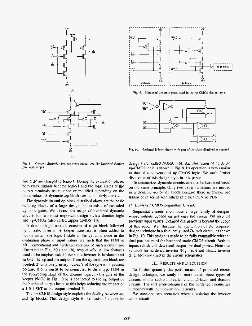
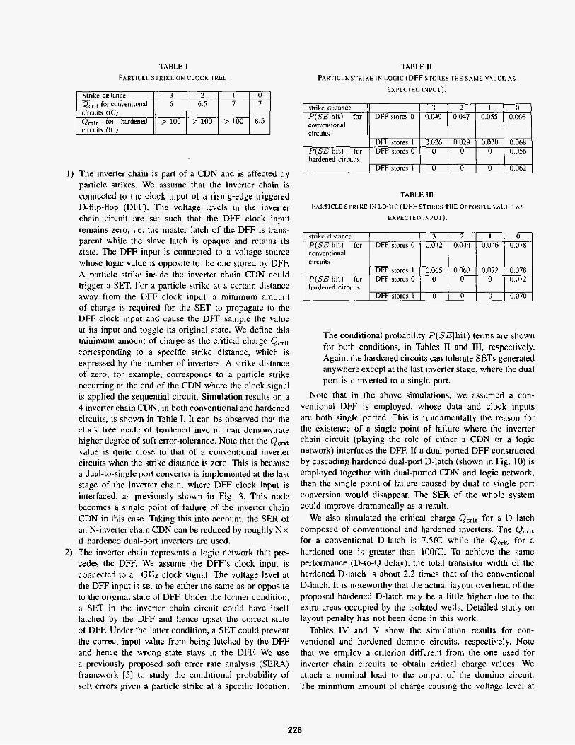
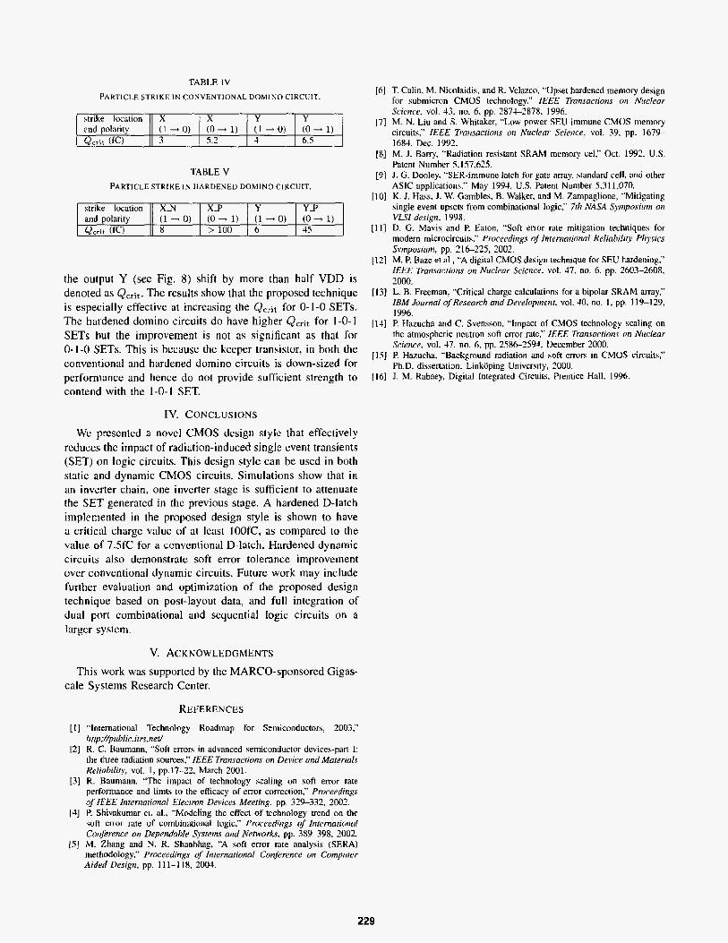