A Circularly Polarized Yagi Antenna System for NTS-I and ... · PDF fileA Circularly Polarized...
26
NIL M mm a owt3 A Circularly Polarized Yagi Antenna System for NTS-I and NTS-2 Ground Stations Louis D. f mrz Space Applications Branch Space Systems Division September 1976 C1I NAVAL RSEARCH LABORATORY w or, du.. Apprwd roe public rsheaee: diseribuno unimi.
Transcript of A Circularly Polarized Yagi Antenna System for NTS-I and ... · PDF fileA Circularly Polarized...
NIL M mm a owt3
A Circularly Polarized Yagi Antenna System forNTS-I and NTS-2 Ground Stations
Louis D. f mrz
Space Applications BranchSpace Systems Division
September 1976
C1I
NAVAL RSEARCH LABORATORYw or, du..
Apprwd roe public rsheaee: diseribuno unimi.
SECURITY CLASSIFICATION OF T1..IS PAGE (When~ 001. Entered)
9 EFRPORTZAOCUETTONAEBFR OPEIGFR
A4 CO I R U L A GENY NO A RED AGORESSIIN S Y S T EM., Final Cop a UMBEUER LA S of l g ~
Loui TRACAT O RNTONMBRADI
I9 ERTISTO SELEEMEN. PROECT TASKRl~
ZAprvefore Lboracrey d.E & OKNTNUBR
WaDsTigton SAEMN D.C. 203 5 *b.,*C Problem R04oc 0,I dl.w-16oReo
IS SUPPLEMENTARY NOTES6
19 1 E C O RLSN OFCEIu NAME ANDjo ADDRESS n-ce.a,5 in4100d- -In y ybok u
Circularly~Sp~r e poaizdya$aten6sse
D4MIp O RGleEC feed syte andFS1 combinatno o f rmC rISSEUTYLA.(othsepn
Apoe fircubl plried ags an-tejnn M ytmfrd ewi.O NvgtinlTcnlg
NSllte NTS- arond stati oun sten atoswsdsneadamdlbutadtse.Threport descedss tedsghooh and comchnatues usdoculcnfucindmnin
\Yor tede , dcalculat e and e asu dpromacshrctsis' I
DD I ON1 1473 EDITION OF I NOV 6531$ OBSOLETE i5,'N 0101-0I4-6601
SECURITY CLASSIFICATION Of THIS PAGE (UM Data Entered) Z
rC LASSI F - f "NOF 1 ?IP A5,h- Dfs EInto,.d)
SECURITY CLASSIFICATION OF THIS PAGE(U"fl Def. gEM...E)

CONTENTS
A. INTRODUCTION ............. ....... 1
B. BACKGROUND.........................................1I
C. DESCRIPTION.......................................... 2
D. CIRCULARITY .......................................... 2
E. IMPEDANCE CHARACTERISTICS ........................... 2
F. IMPEDANCE CALCULATIONS.............................5
G. COMBINING THE TWO YAGIS.............................8
H. CALCULATED RESULTS..................................9
1. MEASURED ANTENNA CHARACTERISTICS..................9
J. PATTERNS............................................ 14
GENERAL REFERENCES ................................... 16
APPENDIX ............................................... Al
............... ... ........
ift
A Circularly Polarized Yagi Antenna System
for
NTS-l and NTS-2 Ground Stations
A. Introduction
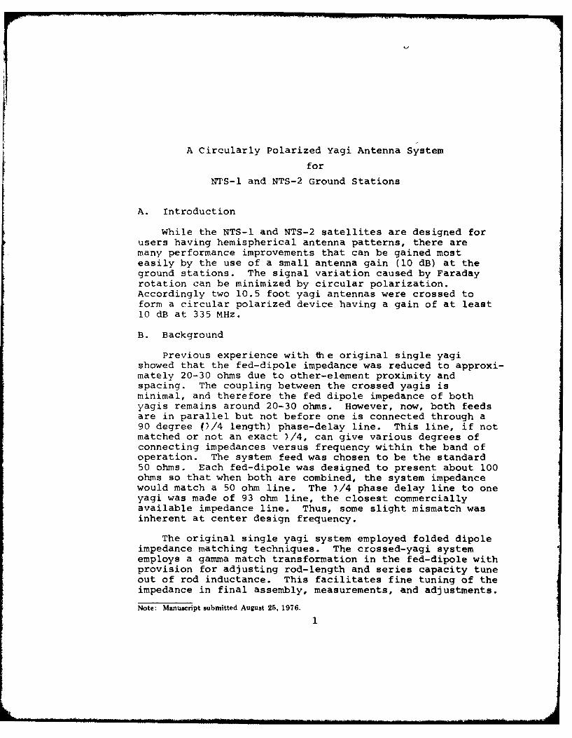
While the NTS-l and NTS-2 satellites are designed forusers having hemispherical antenna patterns, there aremany performance improvements that can be gained mosteasily by the use of a small antenna gain (10 dB) at theground stations. The signal variation caused by Faradayrotation can be minimized by circular polarization.Accordingly two 10.5 foot yagi antennas were crossed toform a circular polarized device having a gain of at least10 dB at 335 MHz.
B. Background
Previous experience with the original single yagishowed that the fed-dipole impedance was reduced to approxi-mately 20-30 ohms due to other-element proximity andspacing. The coupling between the crossed yagis isminimal, and therefore the fed dipole impedance of bothyagis remains around 20-30 ohms. However, now, both feedsare in parallel but not before one is connected through a90 degree ()/4 length) phase-delay line. This line, if notmatched or not an exact )/4, can give various degrees ofconnecting impedances versus frequency within the band ofoperation. The system feed was chosen to be the standard50 ohms. Each fed-dipole was designed to present about 100ohms so that when both are combined, the system impedancewould match a 50 ohm line. The )/4 phase delay line to oneyagi was made of 93 ohm line, the closest commerciallyavailable impedance line. Thus, some slight mismatch wasinherent at center design frequency.
The original single yagi system employed folded dipoleimpedance matching techniques. The crossed-yagi systememploys a gamma match transformation in the fed-dipole withprovision for adjusting rod-length and series capacity tuneout of rod inductance. This facilitates fine tuning of theimpedance in final assembly, measurements, and adjustments.
Note: Manuscript submitted August 25, 1976.

C. Description
The two identical yagis are described best by thesketches of Figure 1, 2 and 3. The boom length in Figure1 is 10 ft - 5 inches and 1.25" (od) diameter. The elementstock is 1/4 inch rod except for the driven elements(2, 2') which are 3/4 inch diameter. The prime numberedelements a-e crossed at 90 with the unprimed ones and arespaced 1.125 inches forward of their corresponding unprimedelements. Elements 1 and ' = 17.82" long.
2 and 2' = 16-50" long. plus end discs(Fig. 3)
3-13 and 3'-13' = 15.84" long.Element spacing from end of boom is:
1 1 inch2 9.253 12.254 15.55 18.756 25.757 39.578 53.439 67.3
10 81.1511 95.0012 108.8713 122.75
The primed elements are spaced 1.125" forward.
D. Circularity
By definition, right hand circularity is that whichrotates clockwise while looking in the direction of anoutgoing signal or transmitted wave. Since the satellitestransmit right hand circularly polarized waves (r.h.c.) theground-based antennas must be r.h.c. To obtain r.h.c. the90 degree phase lag must be applied to the dipole whosecorresponding voltage end is to the right as viewed fromthe rear of the yagi. Thus the quarter wavelength delayline is applied to that dipole.
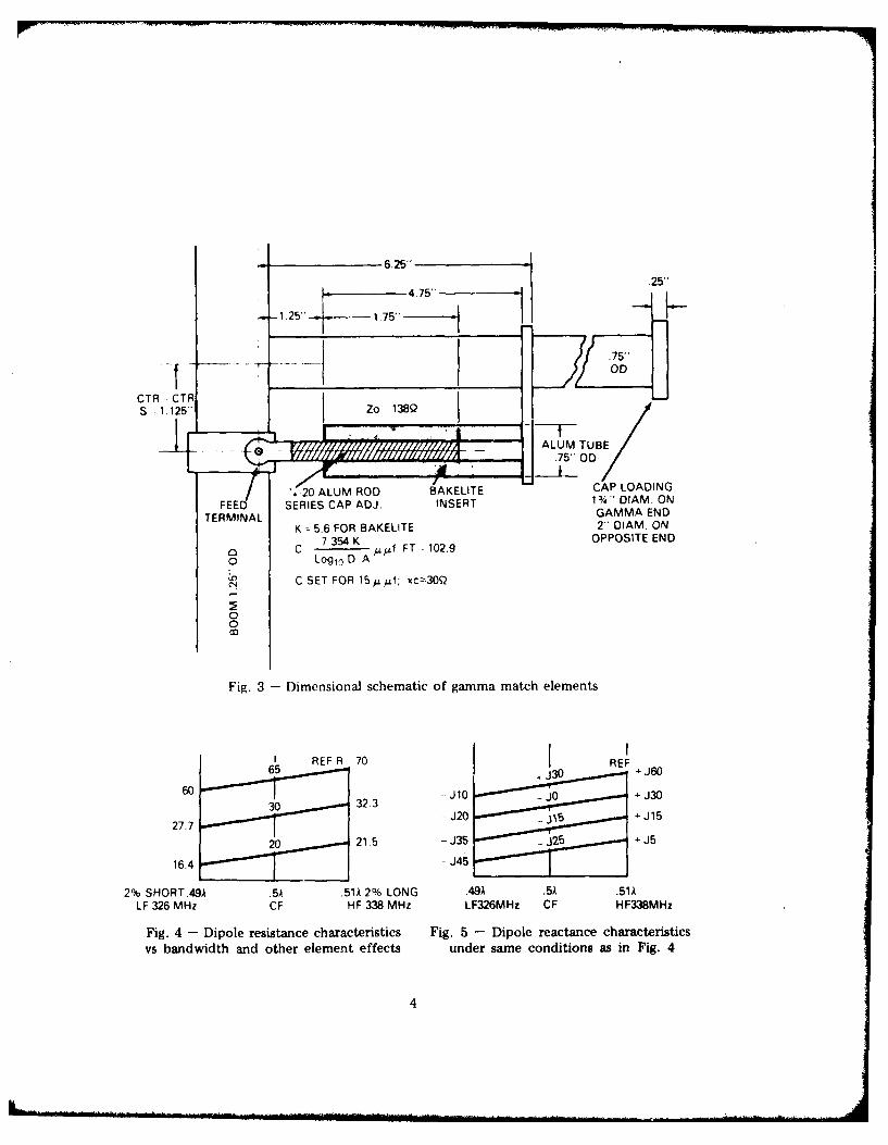
E. Impedance Characteristics
The impedance of a physical /2 dipole of finite thick-ness in free space will run 65-70n + j30 - 40n and mayvary over a band as shown in Figure 4 and 5. These graphsare approximate at best and are extrapolated from thereference curves so marked. The reference curves are fora free-space dipole, but when associated with surroundingparasitic elements of various spacings, the dipoleimpedances may not be so reliably "straight-lined" vs.
2
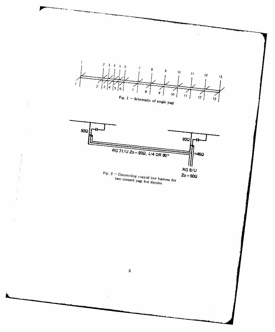
Fig, I - heMatic Of single yagi
RG 7 1 /UZ =.3Q A4 OR 9,==5
RG 8/UFig, 2 - Connecting coaxial lint, hans o Zo 0Qtwo) crossed yagi fed dipol ness o
3e
6.25".25"
125"4175"
-1,25' - -175'
.5OD
'.0 LU RD BAKELITE CAP LOADINGFEED[ SERIES CAP ADJ, INSERT 13/" DIAM. ON
TERMINALGAMMA ENDK 5.6 FOR BAKELITE 2" DIAM. ON
C 7.354 K uu T129OPPOSITE END
LnC SET FOR 15,",uf; xcz30Q
00
Fig. 3 - Dimensional schematic of gamma match elements
61 REF R 70 IREF
60 J10 +J ±J3030 ~ 32.3 j
27.7 J20 j ~ J15
20 21.5 -J35 .j25 + J5
16.4 .... J45
2% SHORT.49A .5A .51A 2% LONG .49A .5A .51 ALF 326 MHz CF HF 338 MHz LF326MHz CF HF338MHz
Fig. 4 - Dipole resistance characteristics Fig. 5 - Dipole reactance characteristicsvs bandwidth and other element effects under same conditions as in Fig. 4
4
frequency. Such complications may alter the agreementbetween calculated and measured impedance characteristics.In the impedance design calculations, the "straight-lines"dipole impedances were used. Therefore, the designedvalues may diffrr over the band from the measured values.The design values should be fairly close to the actual ator near center frequency. Since the dipole rods were manu-factured to be 16.50" long and the half-wave resonant free-space length is 17.785 inches at 332 MHz., they wereobviously too short by a considerable amount. This wasconfirmed in measurements. The reactive component of thefeed impedance would have been in the vicinity of -j70 atcenter frequency instead of a desired -j25. Therefore theresonance was lowered by adding the discs at the ends ofthe two dipole driven elements.
The length of the dipole, due to length-to-diameterratio, where I/d = 17.785 inches/.75 = 24, should bereduced to the value K(/2) = .95 (17.785") = 16.89 inches.Thus the original dipole lengths of 16.50" were short byalmost .4 inch and probably an additional amount shorterbecause of the paralleling of the gamma rod on a portion ofeach dipole stub.
Every indication was that a lowering of the dipoleresonance was necessary by additions to the dipole lengths.
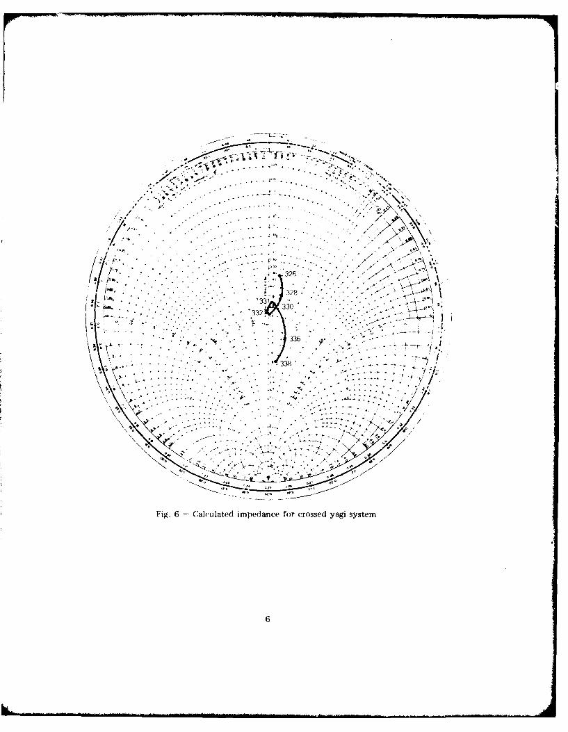
The use of Figures 5 and 6 demonstrate the impedancevariation over a + 2% band and how the matching situationchanges with frequency.
The capacity plates on the dipole ends are for opti-mizing the reactance term of the feed impedance of eachdipole for full band coverage. The diameters of the load-ing discs differ on opposite ends of the dipoles tocompensate for unequal loading due to the gamma rod hard-ware.
F. Impedance Calculations
The calculations will not be exact because, as previ-ously mentioned, the "straight-line" adjusted values ofR + jx of Figures 4 and 5 were assumed. Almost certainly,a complicated set of curves would show if the numerousmutuals of all the parasitic elements were taken intoaccount. The calculated value at center frequency (CF),most likely, will be a close "ball park" value with thisassumption. In practice, the actual reactance can betuned out to a desirable value at CF to give the desiredresults.
5
' .N.
'331
,- . .-- 330
3-32/
336 4~~
33P
33611
Fig. ~ ~ 6* .a-ltdipdnefo rse isse
672
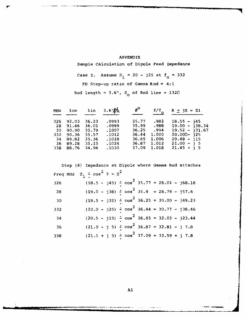
Assuming the fed-dipole impedance was adjusted to becapacitive or -j25n, Z ed = 20 -j25n after all effects ofother elements and dipo e loading are combined at the feedpoint. Now the problem is to design a gamma-rod feed totransform this impedance to 93 + j0f. The procedure whichwas chosen is described below. The appendix gives actualdesign figures. The center frequency of operating designis f = 332 MHz.o
Step 1) As in a folded dipole, assume a diameter androd-to-dipole spacing of, say, 4:1 impedancetransformation ratio.
Step 2) The characteristic impedance of the gamma lineis:
Z = 276 log =2 - 1320 where: S - Ctr-Ctr lineA 1-dl2 spacing
d1d 2 = line diameters
Step 3) Choose a gamma rod length of 3.6 inches or 0
= .101) =36.4a at f =332 MHz; ) =90.36 cm=35.57 inch.
Step 4) The impedance of the dipole where the gamma-rod attaches is:
2Z2 = Zl/Cos ( where Z 1 is the impedance
of the dipole center due to other elementproximity, assumed here to be R - JX=200-j25n.
Step 5) Find the load impedance at the antenna end ofthe gamma line or Z2 times the factor of Step(1). Then normalize to Zo of the Rod linewhich in this case is 1320.
Step 6) Using a Smith Chart, transform the impedanceof Step (5) to the feed terminal or .101Dtoward the generator.
Step 7) The inductive reactance of the rod itself, atfo is Xp = j tan 0.
Step 8) Using a Smith Chart, invert the load impedanceof Step (6) to obtain admittance or Y=G+jB.
Step 9) Also invert the inductive reactance, Xp, ofStep (7) to get Y=G+jB and add together theY's of Step (8) ard Step (9) to get YT*
7
Step 10a) Using a Smith Chart, invert YT of Step (9) toget total impedance, ZT1 3 2 .
Step 10b) Convert the 7 2lj to actual ohms by multiply-ing (Z T32) 0= ) = Z actual.
Now, one has the actual feed terminal impedance of each"iJentical" yagi without any tune-out of gamma-rodinductive reactance. This can be tuned out by the seriescapacity made up of the concentric threaded rod capacitorshown in Fig. 3, where, for the dimensions shown, is about15 pico-farads oresenting X : 31'. This negative
creactance, combined with the Z . of Step (10b) gives a• actuanew or ad]usted actual feed terminal impedance of eachidentical ,,iqi.
G. Combining the Two Yagis
Step 1) Normalize the Z adjusted of each yagi toZo:93 ohm which is the Zo of the 90 degreeohase-shifter line.
Step 2) Combine both Yaqis at the grand junction by,first, calculating the transformed impedanceof one yagi through the )/4 phase shiftersection. Change this to Y=G+jB. The un-transformed yagi impedance is also changed toadimittance so that both can be added inparallel at the grand junction or systemterminal.
17 sho-ild be realized that )/4 transformation of theone yaqi impedance is essentially the equivalent ofobtaining Y=G+jB and the impedance of one can be consideredthe equivalent of the admittance. Therefore only one mustbe transformed and then both added (for identical yagis).
Step 3) Add both admittances at the grand terminal.Using the Smith Chart, invert this totaladmittance to a total feed impedancenormalized to Z,=932.
Step 4) The actual system terminal impedance is thatof Step (3) times Zo=93K.
Step 5) The actual combined feed impedance of Step(4) may be divided by Zo=507 of the main feedline to normalize it to RG8/U - 50 ohm lineto give a Smith Chart impedance plot and todetermine VSWR.
8
I. Calculated Results
A sample calculation of feed impedance is found in theappendix for certain assumed dipole feed characteristics asexplained earlier. Again, due to these assumptions, theimpedance agreement with the actual measured values may beclose at f but are somewhat unpredictable away from fo"
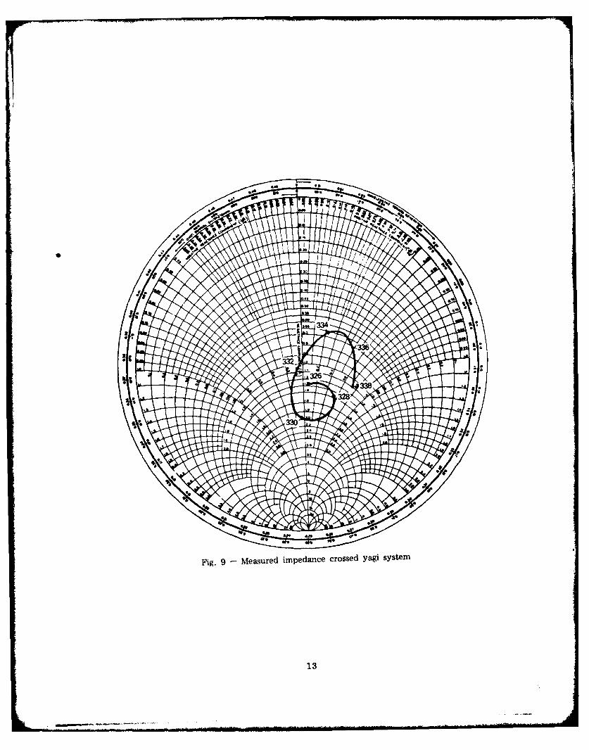
Table 1 and Figure 6 give calculated VSWR and impedancevalues vs frequency. Comparison of impedance in Figure 6at CF=f =332 MHz shows a close agreement with the measuredvalue in Figure 9 but a wide disagreement elsewhere. How-ever the measured and calculated show acceptable valuesover the band.
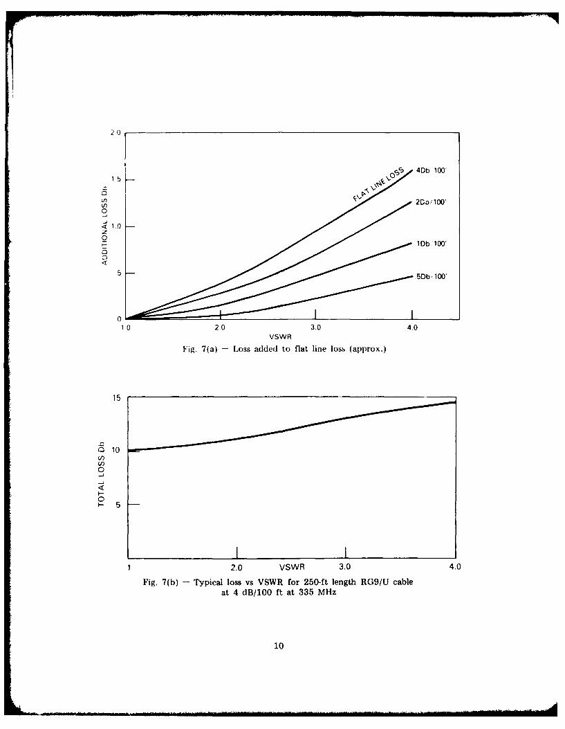
Figure (7a,b) shows additional transmission line lossfor 250 feet of RG 9/U cable. Thus a VSWR of 2:1 wouldadd about 1 dB loss to line loss of 10 dB for 250 feet.
I. Measured Antenna Characteristics
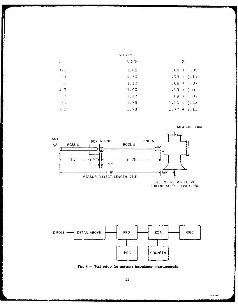
The test equipment set-up consisted of a PRD 3302 VSWRand reflection angle indicator, an 11P608 signal generator,Boonton 320A power amplifier and a Narda 441C VSWR ampli-fier. An HP5245L counter with 5293B plug-in was used toset frequency accurately. Figure 8 shows the block diagramof the impedance measuring set-up with the measured lengthsof line which must be known to derive the impedance values.
The angle of reflection coefficient is (-) when thereflected voltage lags the incident. The angle of 0 of theload (antenna termination) is
0 = 0m+ tO + 720 />
where
9m = angle read from PRD
10 = correction angle from connection planeof PRD adapter to the "tee" center ofthe PRD = 700 at 332 MHz.
Table 2, shows the true values of the impedance at theantenna derived from Om degrees on the instrument for theparticular lengths of connecting lines used in the measur-ing set-up. This crossed yagi impedance is plotted on theSmith Chart of Figure 9. It can be seen from comparisonwith Figure 6, that the impedances are close at centerfrequency and differ out beyond. This difference is due tothe unknown factors and the simple assumptions used in the
2 0
15 4Db 100'
UO 20o/ 100'
1 1D b '100'
5 .5Db; 100'
01 0 2.0 3.0 4.0
VSWR
Fig. 7(a) - Loss added to flat line loss (approx.)
15
Cn
01
1 .68 .6 J 8
1. ~.78 + .11
3oL .13 .89 4+ j.O 7
3 3 1.00 9)3 +~ 0
1.12 .89 Ij.02
1.38 1.26 ± 2
3 ii1.78 1.77 + j .13
MEASURED Om
441 - I 76_
1- 84'1 )
MEASURED ELECT. LENGTH 127.3"
SEE CORRECTION CURVEFOR (Al) SUPPLIED WITH PRD
DIPOLE DETAIL ABOVE PRO H32A68
Fig. 8 - Test setup for antenna impedance measurementsq

2
~~E 0 ) ~-:;~ (An(
32, 1 'E, 3.51 2 1/ 7.0 + 70 70 +7 +7
28 v1 .4 3.54 25.; ) 21.88 + 70 55 -- 43.8 143.8
30 <.s 3.56 2,63 43.20 + 70 -Ili, -1.8 - -1.8
312 . 16 3.58 2573 57.60 + 70 -L 71, 1-47.40 - -47.4
3A b' .2 3.60 25)2 72.00 + 70 * 77 -218.0 -141.0
36 ',i .25 3.62 2,05 86.40 1 70 - 55 =101.4 = 101.4
338 8j.76 3.64 2620 100.80 + 70 -110 = 60.8 = 60.8
Table 3 'i.ows the VSWR, the reflection angle and the derived
antenna terminal impedance for the crossed yagi system.
TABLE 3
Crossed Yagi Impedance
VSWFR Angle Z ant.
326 1.27 +7 1.26 + j.0 2
23 1.75 +43.8 1.35 + j.56
30 1.9 - 1.3 1.9 - j.01
3 .2 1.07 -47.40 1.07 - j.05
1.6 -140.0 .67 1- j.21
1.0 F101.4 .75 + j.5
1. '(160.8 I. 5 j.7
12
132
calculations. The actual VSWR and impedance values, how-ever, are quite useable over the band.
Figure 10 shows VSWR for the Measured and CalculatedCrossed Yagis. Included is a VSWR vs Freq. curve of anearlier single yagi of the folded dipole type drivenelement presently in use. This was included to show thesimilarity in VSWR's for the single and crossed system inthat VSWR drops considerably on the low frequency side ofthe pass band where as the calculated one, due to simpleassumptions described earlier, does not behave in thismanner.
J. Patterns
Calculated axial ratio for the case of Z=20-j25 vsfrequency looking "bore-sight" into the array is shown inTable 4 below.
TABLE 4
Axial Ratio vs. Frequency as Viewed from Array Axis
Freq (MHz) Approx. Axial Ratio and Angle ofMajor Axis
328 3.7 /-22 °
30 1.9 /-27 °
332 1.06 /+3.40
34 1.97 /+360
336 1.41 /900
Calculated axial ratio shows good circularity from 330to 336 and acceptable circularity at 328 MHz.
The antenna field pattern at 332 MHz should be about280 at the 3 dB level with the circularity obtained. Theestimated gain should be about 10-12 dB.
14

00
E
C4-
N CD co N (0 & C1
C c'i
HMSA
154
General References
1. The ARRL Antenna Book, Edition 13, 1974, Amer. RadioRelay League, Inc., Newington, CT.
2. Krauss, John D., Antennas, McGraw-Hill 1950
3. Reference Data for Radio Engineers, 5th Edition,
Howard W. Sons & Co., Inc. (ITT), March, 1969.
4. Reed, H. R. and Russell, Carl M., Ultra High FrequencyPropagation; John Wiley and Sons, Inc., New York 1953(Chapter 8).
16
APPENDIX
Sample Calculation of Dipole Feed Impedance
Case I. Assume Z 1 = 20 - j25 at fo = 332
FD Step-up ratio of Gamma Rod = 4:1
Rod length = 3.6", Z of Rod line = 132n
MHz Xcm lin 3.6-4A 00 f/fo R + 9x = ZI
326 92.03 36.23 .0993 35.77 .982 18.55 - j4528 91.46 36.01 .0999 35.99 .988 19.00 - j38.3430 90.90 35.79 .1007 36.25 .994 19.52 - j31.67
332 90.36 35.57 .1012 36.44 1.000 20.000- j2534 89.82 35.36 .1018 36.65 1.006 20.48 - j1536 89.28 35.15 .1024 36.87 1.012 21.00 - j 5
338 88.76 34.94 .1030 37.09 1.018 21.45 + j 5
Step (4) Impedance at Dipole where Gamma Rod attaches
Freq MHz Z cos 2 e = Z2
326 (18.5 - j45) cos2 35.77 = 28.03 - j68.18
28 (19.0 - j38) Zcos2 35.9 = 28.79 - j57.6
co230 (19.5 - j32) cos 36.25 = 30.00 - j49.23
332 (20.0 - j25) cos2 36.44 = 30.77 - j38.46
34 (20.5 - j15) c 2 36.65 = 32.03 - j23.44
36 (21.0 - j 5) . cos 2 36.87 = 32.81 - j 7.8
2338 (21.5 + j 5) cos 37.09 = 33.59 + j 7.8
Al
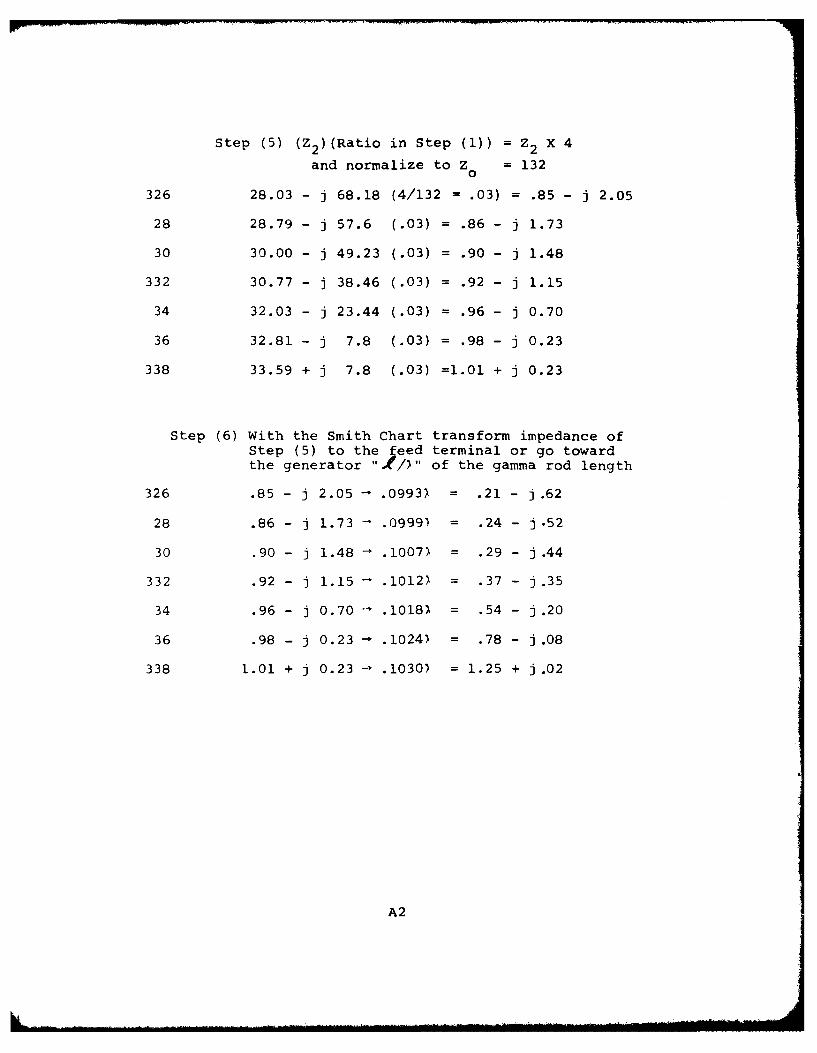
Step (5) (Z 2 )(Ratio in Step (1)) = Z2X 4
and normalize to Z =1320
326 28.03 - j 68.18 (4/132 =.03) = .85 - j 2.05
28 28.79 - j 57.6 (.03) =.86 - j 1.73
30 30.00 - j 49.23 (.03) =.90 - j 1.48
332 30.77 - j 38.46 (.03) =.92 - j 1.15
34 32.03 - j 23.44 (.03) =.96 - j 0.70
36 32.81 - j 7.8 (.03) =.98 - j 0.23
338 33.59 + j7.8 (.03) =1.01 + j 0.23
Step (6) With the Smith Chart transform impedance ofStep (5) to the feed terminal or go towardthe generator ".el),. of the gamma rod length
326 .85 - j 2.05 -~ .099D~ .21 - j .62
28 .86 - j1.73 -~ .0999) .24 - j-52
30 .90 - j1.48 - .1007 .29 - j .44
332 .92 - j 1.15 - .101D~ .37 - j .35
34 .96 - j 0.70 - .1018) .54 - j .20
36 .98 - j 0.23 - .1024) = .78 - j.08
338 1.01 + j 0.23 - .1030) =1.25 + j.02
A2
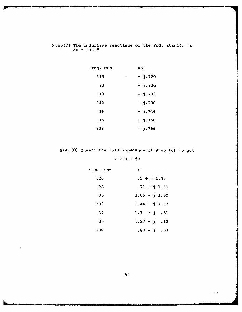
Step(7) The inductive reactance of the rod, itself, isXp tan 0
Freq. MHz Xp
326 = + j.720
28 + j.726
30 + j. 73 3
332 + j .738
34 + j.744
36 + j.750
338 + j.756
Step(8) Invert the load impedance of Step (6) to get
Y =G + jB
Freq. MHz Y
326 .5 + j 1.45
28 .71 + j 1.59
30 1.05 + j 1.60
332 1.44 + j 1.38
34 1.7 + j .61
36 1.27 + j .12
338 .80 - j .03
A3
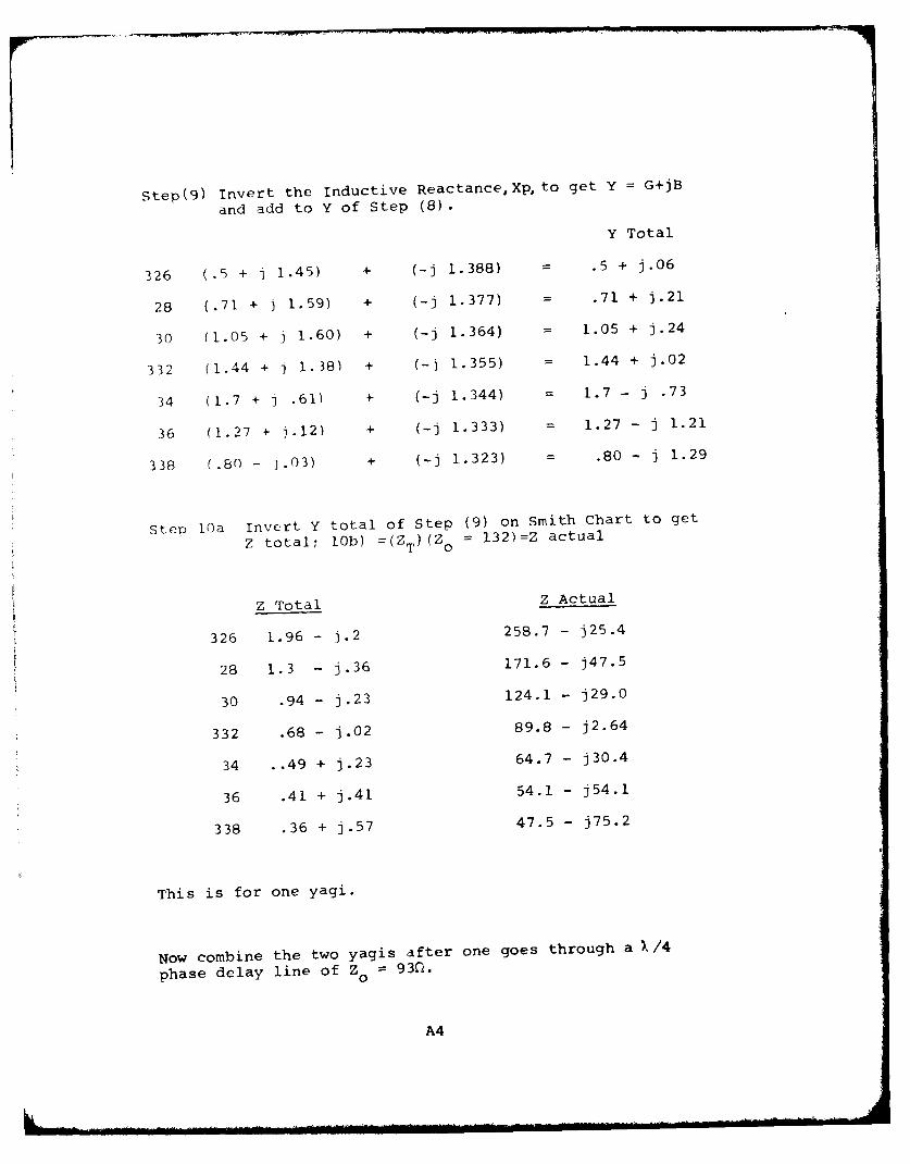
Step(9) Invert the Inductive Reactance, Xp, to get Y = G+jB
and add to Y of Step (8).
Y Total
326 (.5 + j 1.45) + (-j 1.388) .5 + j.06
28 (.71 + j 1.59) + (-j 1.377) = .71 + j.21
30 (1.05 + j 1.60) + (-j 1.364) 1.05 + j.24
332 (1.44 + j 1.38) + (-j 1.355) 1.44 + j.02
34 (1.7 + j .61) + (-j 1.344) = 1.7- j .73
36 (1.27 + j.12) + (-j 1.333) 1.27 - j 1.21
338 (.80 - ).03) + (-j 1.323) = .80- j 1.29
Ste 10a Invert Y total of Step (9) on Smith Chart to get
Z total; 10b) =(ZT)(ZO 132)=Z actual
Z Total Z Actual
326 1.96 - j.2 258.7 - j25.4
28 1.3 - j.36 171.6- j47.5
30 .94 - j.23 124.1 - j29.0
332 .68 - j.02 89.8- j2.64
34 ..49 + j.23 64.7 - j30.4
36 .41 + j.41 54.1 - j54.1
338 .36 + j.57 47.5 - j75.2
This is for one yagi.
Now combine the two yagis after one goes through a X/4
phase delay line of Zo = 93C.
A4
G. Combining the Two Yagis
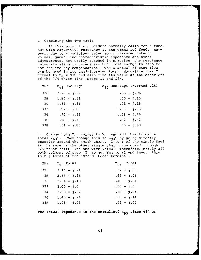
At this point the procedure normally calls for a tune-out with capacitive reactance at the gamma-rod feed. How-ever, due to a judicious selection of assumed antennavalues, gamma line characteristic impedance and otheradjustments, not easily reached in practice, the reactancevalue was slightly capacitive but close enough to zero tonot require any compensation. The Z actual of step (10a)can be used in its unadulterated form. Normalize this Zactual to Zo = 931 and also find its value at the other endof the 1/4 phase line (Steps G1 and G2).
MHz Z93 One Yagi Z93 One Yagi inverted .25
326 2.78 - j.27 .36 + j.06
28 1.85 - j.51 .50 + j.15
30 1.33 - j.31 .71 + j.18
332 .97 - j.03 1.03 + j.03
34 .70 - j.33 1.38 + j.26
36 .58 + j.58 .82 - j.82
338 .51 + j.85 .55 - j.90
3. Change both Z values to Y and add them to get atotal Y9 3 T. Then change this to Z9 3T by going directlyopposite around the Smith Chart. Z to Y of the single Yagiis the same as the other single yagi transformed through'/4 nhase shift line and vice-versa. Therefore, merely addboth columns of step (2) to get Y9 3 total and invert thisto Z 9 3 total at the "Grand Feed" terminal.
MHz Y93 Total Z93 Total
326 3.14 - j.21 .32 + j.05
28 2.35 - j.36 .42 + j.06
30 2.04 - j.13 .48 + j.04
332 2.00 + j.0 .50 + j.0
34 2.08 - j.07 .48 + j.01
36 1.40 - j.24 .68 + j.14
338 1.06 - j.05 .96 + j.07
The actual impedance is the normalized Z93 times 930 or
A5
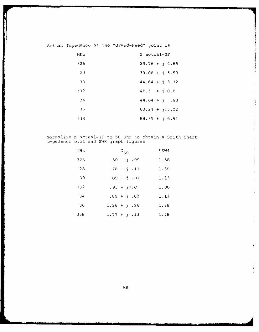
Actual rmpcdance at the "Grand-Feed" point is
MHz Z actual-GF
326 29.76 + j 4.65
28 39.06 + j 5.58
30 44.64 + j 3.72
332 46.5 + j 0.0
34 44.64 + j .93
36 63.24 + j13.02
338 88.35 + j 6.51
Normalize Z actual-GF to 50 ohm to obtain a Smith Chart
impedance plot and SWR graph figures
MHz Z VSW4
326 .60 + j .09 1.68
28 .78 + § .11 1.30
30 .89 + j .07 1.13
332 .93 + jO.0 1.00
34 .89 + j .02 1.12
36 1.26 + j .26 1.38
338 1.77 + j .13 1.78
A6