96kHz Digital Audio Transmitter - TI.com
27
DIT4096 SBOS225B – DECEMBER 2001 – REVISED JUNE 2003 www.ti.com DESCRIPTION The DIT4096 is a digital audio transmitter designed for use in both professional and consumer audio applications. Trans- mit data rates up to 96kHz are supported. The DIT4096 supports both software and hardware operation, which makes it suitable for applications with or without a microcontroller. A flexible serial audio interface is provided, supporting stan- dard audio data formats and easy interfacing to audio DSP serial ports. PRODUCTION DATA information is current as of publication date. Products conform to specifications per the terms of Texas Instruments standard warranty. Production processing does not necessarily include testing of all parameters. Copyright © 2001-2003, Texas Instruments Incorporated 96kHz Digital Audio Transmitter FEATURES ● COMPLIANT WITH AES-3, IEC-60958, AND EIAJ CP1201 INTERFACE STANDARDS ● SUPPORTS SAMPLING RATES UP TO 96kHz ● SUPPORTS MONO-MODE OPERATION ● ON-CHIP DIFFERENTIAL LINE DRIVER ● FLEXIBLE AUDIO SERIAL INTERFACE: -Master or Slave Mode Operation -Supports I 2 S, Left-Justified, and Right-Justified Data Formats ● SOFTWARE MODE VIA SERIAL CONTROL INTERFACE: -Block Sized Buffer for Channel Status Data -Auto Increment Mode for Block Sized Write and Read Operations ● HARDWARE MODE ALLOWS OPERATION WITH- OUT A MICROCONTROLLER ● CRC CODE GENERATION FOR PROFESSIONAL MODE ● MASTER CLOCK RATE: 256f S , 384f S , or 512f S ● +5V CORE SUPPLY (V DD ) ● +2.7V TO V DD LOGIC I/O SUPPLY (V IO ) ● PACKAGE: TSSOP-28 APPLICATIONS ● DIGITAL MIXING CONSOLES ● DIGITAL MICROPHONES ● DIGITAL AUDIO WORKSTATIONS ● BROADCAST STUDIO EQUIPMENT ● EFFECTS PROCESSORS ● SURROUND-SOUND DECODERS AND ENCODERS ● A/V RECEIVERS ● DVD, CD, DAT, AND MD PLAYERS ● AUDIO TEST EQUIPMENT DIT4096 Please be aware that an important notice concerning availability, standard warranty, and use in critical applications of Texas Instruments semiconductor products and disclaimers thereto appears at the end of this data sheet. All trademarks are the property of their respective owners.
Transcript of 96kHz Digital Audio Transmitter - TI.com
DIT4096
SBOS225B – DECEMBER 2001 – REVISED JUNE 2003
www.ti.com
DESCRIPTIONThe DIT4096 is a digital audio transmitter designed for usein both professional and consumer audio applications. Trans-mit data rates up to 96kHz are supported. The DIT4096supports both software and hardware operation, which makesit suitable for applications with or without a microcontroller. Aflexible serial audio interface is provided, supporting stan-dard audio data formats and easy interfacing to audio DSPserial ports.
PRODUCTION DATA information is current as of publication date.Products conform to specifications per the terms of Texas Instrumentsstandard warranty. Production processing does not necessarily includetesting of all parameters.
Copyright © 2001-2003, Texas Instruments Incorporated
96kHz Digital Audio Transmitter
FEATURES COMPLIANT WITH AES-3, IEC-60958, AND EIAJ
CP1201 INTERFACE STANDARDS SUPPORTS SAMPLING RATES UP TO 96kHz SUPPORTS MONO-MODE OPERATION ON-CHIP DIFFERENTIAL LINE DRIVER FLEXIBLE AUDIO SERIAL INTERFACE:
-Master or Slave Mode Operation-Supports I2S, Left-Justified, and Right-JustifiedData Formats
SOFTWARE MODE VIA SERIAL CONTROLINTERFACE:-Block Sized Buffer for Channel Status Data-Auto Increment Mode for Block Sized Write andRead Operations
HARDWARE MODE ALLOWS OPERATION WITH-OUT A MICROCONTROLLER
CRC CODE GENERATION FOR PROFESSIONALMODE
MASTER CLOCK RATE: 256fS, 384fS, or 512fS
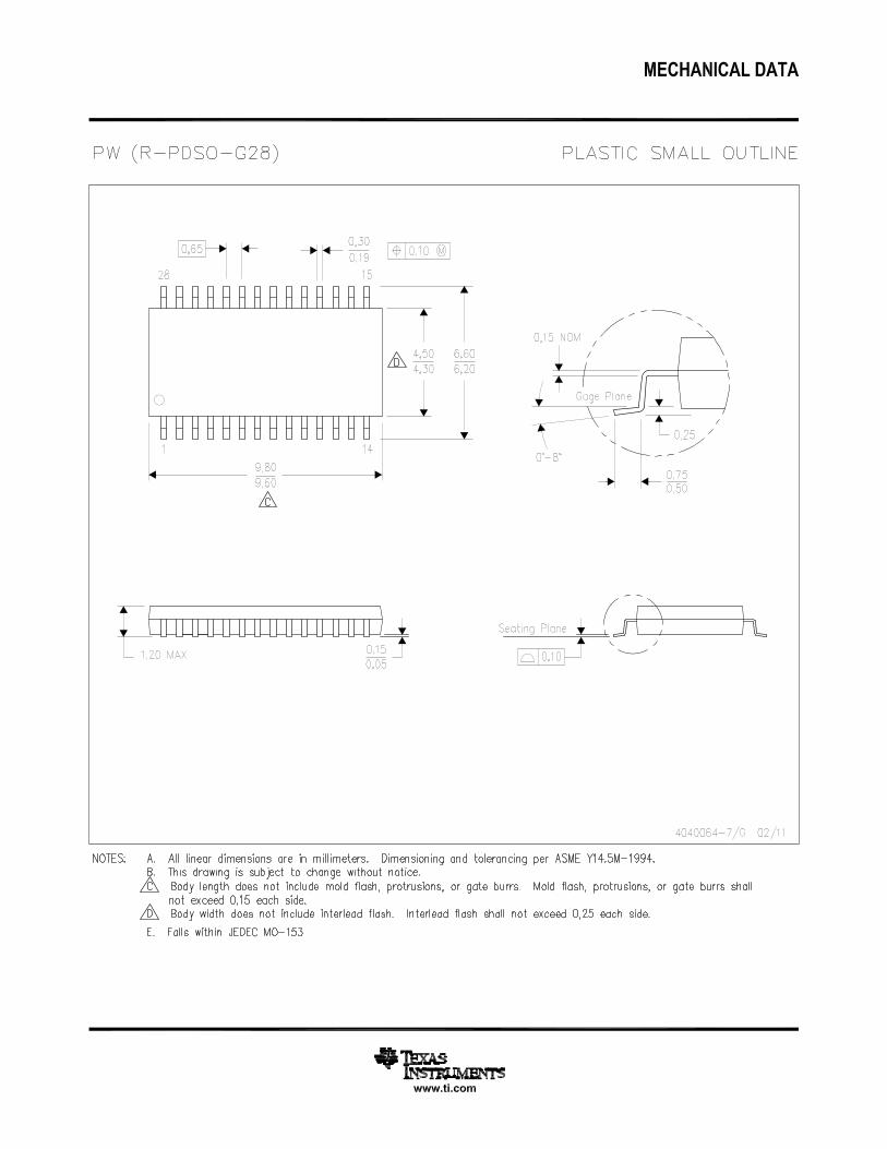
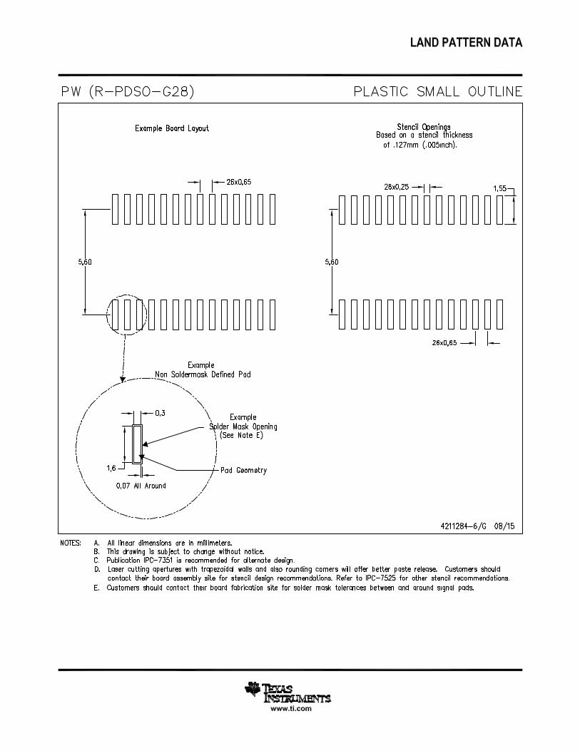
+5V CORE SUPPLY (VDD) +2.7V TO VDD LOGIC I/O SUPPLY (VIO) PACKAGE: TSSOP-28
APPLICATIONS DIGITAL MIXING CONSOLES DIGITAL MICROPHONES DIGITAL AUDIO WORKSTATIONS BROADCAST STUDIO EQUIPMENT EFFECTS PROCESSORS SURROUND-SOUND DECODERS AND ENCODERS A/V RECEIVERS DVD, CD, DAT, AND MD PLAYERS AUDIO TEST EQUIPMENT
DIT4096
Please be aware that an important notice concerning availability, standard warranty, and use in critical applications ofTexas Instruments semiconductor products and disclaimers thereto appears at the end of this data sheet.
All trademarks are the property of their respective owners.
DIT40962SBOS225Awww.ti.com
Power-Supply Voltage, VDD .............................................................. +6.5VVIO .............................................................. +6.5V
Input Current ................................................................................... ±10mADigital Input Voltage .......................................................... –0.2V to +5.5VDigital Output Voltage ............................................ –0.2V to (VDD + 0.2V)Power Dissipation .......................................................................... 300mWOperating Temperature Range ........................................ –40°C to +85°CStorage Temperature ..................................................... –55°C to +125°CLead Temperature (soldering, 5s) ................................................. +260°CPackage Temperature (IR re-flow, 10s) ........................................ +235°C
ABSOLUTE MAXIMUM RATINGS(1) ELECTROSTATICDISCHARGE SENSITIVITY
This integrated circuit can be damaged by ESD. Texas Instru-ments recommends that all integrated circuits be handled withappropriate precautions. Failure to observe proper handlingand installation procedures can cause damage.
ESD damage can range from subtle performance degradationto complete device failure. Precision integrated circuits may bemore susceptible to damage because very small parametricchanges could cause the device not to meet its publishedspecifications.
PACKAGE/ORDERING INFORMATIONSPECIFIED
PACKAGE TEMPERATURE PACKAGE ORDERING TRANSPORTPRODUCT PACKAGE-LEAD DESIGNATOR(1) RANGE MARKING NUMBER MEDIA, QUANTITY
DIT4096 TSSOP-28 PW –40°C to +85°C DIT4096IPW DIT4096IPW Rails, 50" " " " " DIT4096IPWR Tape and Reel, 2000
NOTE: (1) For the most current specifications and package information, refer to our web site at www.ti.com.
NOTE: (1) Stresses above these ratings may cause permanent damage.Exposure to absolute maximum conditions for extended periods may degradedevice reliability. These are stress ratings only, and functional operation of thedevice at these or any other conditions beyond those specified is not implied.
DIT4096 3SBOS225A www.ti.com
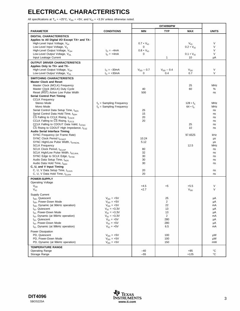
ELECTRICAL CHARACTERISTICSAll specifications at TA = +25°C, VDD = +5V, and VIO = +3.3V unless otherwise noted.
DIT4096IPW
PARAMETER CONDITIONS MIN TYP MAX UNITS
DIGITAL CHARACTERISTICSApplies to All Digital I/O Except TX+ and TX–
High-Level Input Voltage, VIH 0.7 • VIO VIO VLow-Level Input Voltage, VIL 0 0.2 • VIO VHigh-Level Output Voltage, VOH IO = –4mA 0.8 • VIO VLow-Level Output Voltage, VOL IO = +4mA 0 0.1 • VIO VInput Leakage Current 1 10 µA
OUTPUT DRIVER CHARACTERISTICSApplies Only to TX+ and TX–
High-Level Output Voltage, VOH IO = –30mA VDD – 0.7 VDD – 0.4 VDD VLow-Level Output Voltage, VOL IO = +30mA 0 0.4 0.7 V
SWITCHING CHARACTERISTICSMaster Clock and Reset
Master Clock (MCLK) Frequency 25 MHzMaster Clock (MCLK) Duty Cycle 40 60 %Reset (RST) Active Low Pulse Width 500 ns
Serial Control Port TimingCCLK Frequency
Stereo Mode fS = Sampling Frequency 128 • fS MHzMono Mode fS = Sampling Frequency 64 • fS MHz
Serial Control Data Setup Time, tSDS 25 nsSerial Control Data Hold Time, tSDH 15 nsCS Falling to CCLK Rising, tCSCR 20 nsCCLK Falling to CS Rising, tCFCS 20 nsCCLK Falling to CDOUT Data Valid, tCFDO 25 nsCS Rising to CDOUT High Impedance, tCSZ 10 ns
Audio Serial Interface TimingSYNC Frequency (or Frame Rate) 97.6525 kHzSYNC Clock Period tSYNCP 10.24 µsSYNC High/Low Pulse Width, tSYNCHL 5.12 µsSCLK Frequency 12.5 MHzSCLK Clock Period, tSCLKP 80 nsSCLK High/Low Pulse Width, tSCLKHL 32 nsSYNC Edge to SCLK Edge, tSYSK 30 nsAudio Data Setup Time, tADS 30 nsAudio Data Hold Time, tADH 30 ns
C, U, and V Input TimingC, U, V Data Setup Time, tCUVS 20 nsC, U, V Data Hold Time, tCUVH 20 ns
POWER-SUPPLYOperating Voltage
VDD +4.5 +5 +5.5 VVIO +2.7 VDD V
Supply CurrentIDD, Quiescent VDD = +5V 25 µAIDD, Power-Down Mode VDD = +5V 2 µAIDD, Dynamic (at 96kHz operation) VDD = +5V 22 mAIIO, Quiescent VIO = +3.3V 13 µAIIO, Power-Down Mode VIO = +3.3V 13 µAIIO, Dynamic (at 96kHz operation) VIO = +3.3V 2 mAIIO, Quiescent VIO = +5V 280 µAIIO, Power-Down Mode VIO = +5V 280 µAIIO, Dynamic (at 98kHz operation) VIO = +5V 6.5 mA
Power DissipationPD, Quiescent VDD = +5V 100 µWPD, Power-Down Mode VDD = +5V 100 µWPD, Dynamic (at 96kHz operation) VDD = +5V 150 mW
TEMPERATURE RANGEOperating Range –40 +85 °CStorage Range –55 +125 °C

DIT40964SBOS225Awww.ti.com
PIN CONFIGURATION: Software Mode (MODE = 0)
Top View TSSOP
PIN DESCRIPTIONS: Software Mode
PIN NAME PIN DESCRIPTION
1 NC No Connection2 CDOUT Control Port Data Output, Tri-State3 CCLK Control Port Data Clock Input4 CDIN Control Port Serial Data Input5 CS Control Port Chip Select Input, Active LOW6 MCLK Master Clock Input7 VIO Digital I/O Power Supply, +2.7V to VDD
Nominal8 DGND Digital Ground9 RXP AES-3 Encoded Data Input10 NC No Connection11 SCLK Audio Serial Port Data Clock I/O12 SYNC Audio Serial Port Frame SYNC Clock I/O13 SDATA Audio Serial Port Data Input14 NC No Connection15 RST Reset Input, Active LOW16 DGND Digital Ground17 TX– Transmitter Line Driver Output18 TX+ Transmitter Line Driver Output19 VDD Digital Core Power Supply, +5V Nominal20 NC No Connection21 NC No Connection22 INT Open Drain Interrupt Output, Active LOW.
Requires 10kΩ pull-up resistor to VIO.23 NC No Connection24 NC No Connection25 BLS Block Start I/O26 NC No Connection27 U User Data Input28 MODE Control Mode Input. Set MODE = 0 for
Software Mode operation.
NC
CDOUT
CCLK
CDIN
CS
MCLK
VIO
DGND
RXP
NC
SCLK
SYNC
SDATA
NC
MODE
U
NC
BLS
NC
NC
INT
NC
NC
VDD
TX+
TX–
DGND
RST
1
2
3
4
5
6
7
8
9
10
11
12
13
14
28
27
26
25
24
23
22
21
20
19
18
17
16
15
DIT4096
PIN CONFIGURATION: Hardware Mode (MODE = 1)
CSS
COPY/C
L
CLK1
CLK0
MCLK
VIO
DGND
FMT0
FMT1
SCLK
SYNC
SDATA
M/S
MODE
U
V
BLS
BLSM
EMPH
AUDIO
MONO
MDAT
VDD
TX+
TX–
DGND
RST
1
2
3
4
5
6
7
8
9
10
11
12
13
14
28
27
26
25
24
23
22
21
20
19
18
17
16
15
DIT4096
Top View TSSOP
PIN DESCRIPTIONS: Hardware Mode
PIN NAME PIN DESCRIPTION
1 CSS Channel Status Data Mode Input2 COPY/C Copy Protect Input or Channel Status Se-
rial Data Input3 L Generation Status Input4 CLK1 Master Clock Rate Selection Input5 CLK0 Master Clock Rate Selection Input6 MCLK Master Clock Input7 VIO Digital I/O Power Supply, +2.7V to VDD
Nominal8 DGND Digital Ground9 FMT0 Audio Data Format Control Input10 FMT1 Audio Data Format Control Input11 SCLK Audio Serial Port Data Clock I/O12 SYNC Audio Serial Port Frame SYNC Clock I/O13 SDATA Audio Serial Port Data Input14 M/S Audio Serial Port Master/Slave Control Input15 RST Reset Input, Active LOW16 DGND Digital Ground17 TX– Transmitter Line Driver Output18 TX+ Transmitter Line Driver Output19 VDD Digital Core Power-Supply, +5V Nominal20 MDAT Mono Mode Channel Data Selection Input21 MONO Mono Mode Enable Input, Active HIGH22 AUDIO Audio Data Valid Control Input, Active LOW23 EMPH Pre-Emphasis Status Input, Active LOW24 BLSM Block Start Mode Control Input25 BLS Block Start I/O26 V Validity Data Input27 U User Data Input28 MODE Control Mode Input. Set MODE = 1 for
Hardware Mode Operation.

DIT4096 5SBOS225A www.ti.com
GENERAL DESCRIPTIONThe DIT4096 is a complete digital audio transmitter, suitablefor both professional and consumer audio applications. Sam-pling rates up to 96kHz are supported. The DIT4096 com-plies with the requirements for the AES-3, IEC-60958, andEIAJ CP1201 interface standards.
Figures 1 and 2 show the block diagrams for the DIT4096when used in Software and Hardware control modes. TheMODE input (pin 28) determines the control model used toconfigure the DIT4096 internal functions. In Software mode,a serial control port is used to write and read on-chip controlregisters and status buffers. In Hardware mode, dedicatedcontrol pins are provided for configuration and status inputs.
The DIT4096 includes an audio serial port, which is used tointerface to standard digital audio sources, such as
AudioSerialPort
AES-3 Encoder
LineDriver
ResetLogic
Serial Control Interface,Control Registers,
and Channel StatusData Buffers
ClockGenerator
RXP
TX+
TX–
MCLK
U
SYNC
SCLK
SDATA
RST
Control PortBLSINT
AudioSerialPort
AES-3 EncoderLine
Driver
ResetLogic
CUVData Buffer
ClockGenerator
TX+
TX–
MCLK
CLK1
BLSMBLSMONOMDAT
CLK0
SYNCSCLK
SDATA
M/SFMT0FMT1
CSSCOPY/C
LAUDIOEMPH
UV
RST
Analog-to-Digital (A/D) converters, Digital Signal Processors(DSPs), and audio decoders. Support for Left-Justified, Right-Justified, and I2S data formats is provided.
The AES-3 encoder creates a multiplexed bit stream, con-taining audio, status, and user data. See Figure 3 for themultiplexed data format. The data is then Bi-Phase Markencoded and output to a differential line driver. The line driveroutputs are connected to the transmission medium, be itcable or fiber optics. In the case of twisted-pair or coaxialcable, a transformer is commonly used to couple the driveroutputs to the transmission line. This provides both isolationand improved common-mode rejection. For optical transmis-sion, the TX+ (pin 18) driver output is connected to an opticaltransmitter module. See the Applications Information sectionof this data sheet for details regarding output driver circuitconfigurations.
FIGURE 1. Software Mode Block Diagram.
FIGURE 2. Hardware Mode Block Diagram.
DIT40966SBOS225Awww.ti.com
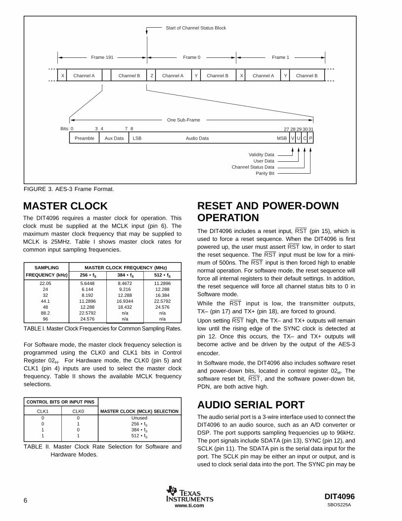
MASTER CLOCKThe DIT4096 requires a master clock for operation. Thisclock must be supplied at the MCLK input (pin 6). Themaximum master clock frequency that may be supplied toMCLK is 25MHz. Table I shows master clock rates forcommon input sampling frequencies.
Channel AX X YYZ Channel A Channel A Channel BChannel BChannel B
Frame 191 Frame 0 Frame 1
Start of Channel Status Block
One Sub-Frame
Preamble Aux Data LSB MSB V U C P
27 28 29 30 31
Audio Data
Validity DataUser Data
Parity BitChannel Status Data
Bits: 0 3 4 7 8
FIGURE 3. AES-3 Frame Format.
MASTER CLOCK FREQUENCY (MHz)
256 • fS 384 • fS 512 • fS
SAMPLING
FREQUENCY (kHz)
22.05 5.6448 8.4672 11.289624 6.144 9.216 12.28832 8.192 12.288 16.384
44.1 11.2896 16.9344 22.579248 12.288 18.432 24.576
88.2 22.5792 n/a n/a96 24.576 n/a n/a
TABLE I. Master Clock Frequencies for Common Sampling Rates.
For Software mode, the master clock frequency selection isprogrammed using the CLK0 and CLK1 bits in ControlRegister 02H. For Hardware mode, the CLK0 (pin 5) andCLK1 (pin 4) inputs are used to select the master clockfrequency. Table II shows the available MCLK frequencyselections.
RESET AND POWER-DOWNOPERATIONThe DIT4096 includes a reset input, RST (pin 15), which isused to force a reset sequence. When the DIT4096 is firstpowered up, the user must assert RST low, in order to startthe reset sequence. The RST input must be low for a mini-mum of 500ns. The RST input is then forced high to enablenormal operation. For software mode, the reset sequence willforce all internal registers to their default settings. In addition,the reset sequence will force all channel status bits to 0 inSoftware mode.
While the RST input is low, the transmitter outputs,TX– (pin 17) and TX+ (pin 18), are forced to ground.
Upon setting RST high, the TX– and TX+ outputs will remainlow until the rising edge of the SYNC clock is detected atpin 12. Once this occurs, the TX– and TX+ outputs willbecome active and be driven by the output of the AES-3
encoder.
In Software mode, the DIT4096 also includes software resetand power-down bits, located in control register 02H. Thesoftware reset bit, RST, and the software power-down bit,PDN, are both active high.
AUDIO SERIAL PORTThe audio serial port is a 3-wire interface used to connect theDIT4096 to an audio source, such as an A/D converter orDSP. The port supports sampling frequencies up to 96kHz.The port signals include SDATA (pin 13), SYNC (pin 12), andSCLK (pin 11). The SDATA pin is the serial data input for theport. The SCLK pin may be either an input or output, and isused to clock serial data into the port. The SYNC pin may be
CONTROL BITS OR INPUT PINS
CLK1 CLK0 MASTER CLOCK (MCLK) SELECTION0 0 Unused0 1 256 • fS1 0 384 • fS1 1 512 • fS
TABLE II. Master Clock Rate Selection for Software andHardware Modes.

DIT4096 7SBOS225A www.ti.com
either an input or output, and provides the frame synchroni-zation clock for the port. The SYNC pin is also used as a datalatch clock for the channel status, user, and validity datainputs in Hardware mode, and the user data input in Softwaremode.
SLAVE OR MASTER MODE OPERATIONThe audio serial port supports both Slave and Master modeoperation. In Slave mode, both SYNC and SCLK are config-ured as inputs. The audio source device must generate boththe SYNC and SCLK clocks in Slave mode. In Master mode,both SYNC and SCLK are configured as outputs. The audioserial port generates the SYNC and SCLK clocks in Mastermode, deriving both from the master clock (MCLK) input.
In Software mode, Master/Slave mode selection is per-formed using the M/S bit in Control Register 03H (defaults toSlave mode). In Hardware mode, the M/S input (pin 14) isused to select the audio serial port mode. This is shown inTable III.
CONTROL BITS OR INPUT PIN
M/S MASTER/SLAVE MODE SELECTION
Slave Mode; both SYNC and SCLKare inputs.
Master Mode; both SYNC and SCLKare outputs.
TABLE III. Master/Slave Mode Selection for Software orHardware Mode.
0
1
SYNC AND SCLK FREQUENCIESThe SYNC clock rate is the same as the sampling frequency,or fS. This holds true for both Slave and Master modes. TheDIT4096 supports SYNC frequencies up to 96kHz.
The SCLK frequency in Slave mode must provide at leastone clock cycle for each data bit that is input at SDATA. Themaximum SCLK frequency is 128 • fS, or 12.288MHz forfS = 96kHz. The SCLK frequency in Master mode is set bythe DIT4096 itself. For Software mode operation, the SCLKrate may be programmed to either 64 • fS or 128 • fS, usingthe SCLKR bit in Control Register 03H. In Hardware mode,the SCLK frequency is fixed at 64 • fS for Master mode.
AUDIO DATA FORMATSThe DIT4096 supports standard audio data formats, includ-ing Philips I2S, Left-Justified, and Right-Justified data.
Software mode provides the most flexible format selection,while Hardware mode supports a limited subset of theSoftware mode formats. Linear PCM audio data at theSDATA input is typically presented in Binary Two’s Comple-ment, MSB first format. Encoded or non-audio data may beprovided as required by the encoding scheme in use. Figure4 shows the common data formats used by the audio serialport.
tSYNCHL tSYNCHL
tSYSK
tSYSKHL tSCLKHL
tSCLKP
tADS tADH
MSB LSB
MSB LSB
MSB LSB
MSB LSB
MSB LSB
MSB LSB Right Justified
Left Justified0 SCLK Delay
Left Justified1 SCLK Delay (I2S)
Right ChannelLeft Channel
SYNC(ISYNC = 0)
SYNC(ISYNC = 1)
SCLK(ISCLK = 0)
SCLK(ISCLK = 1)
SYNC
SCLK
SDATA
SDATA
SDATA
SDATA
FIGURE 4. Audio Data Formats and Timing.
DIT40968SBOS225Awww.ti.com
AUDIO DATA
FORMATS
CONTROL REGISTER 03H BIT SETTINGS
Bit Name Function Bit Name Function Bit Name Function Bit Name Function
JUS Justification DELAY SCLK Delay ISCLK Sampling Edge ISYNC Phase
Phillips I2S 0 Left-Justified 1 1 SCLK Delay 0 Rising Edge 1 InvertedLeft-Justified 0 Left-Justified 0 0 SCLK Delay 0 Rising Edge 0 NoninvertedRight-Justified 1 Right-Justified 0 0 SCLK Delay 0 Rising Edge 0 Noninverted
TABLE IV. Audio Data Format Selection in Software Mode.
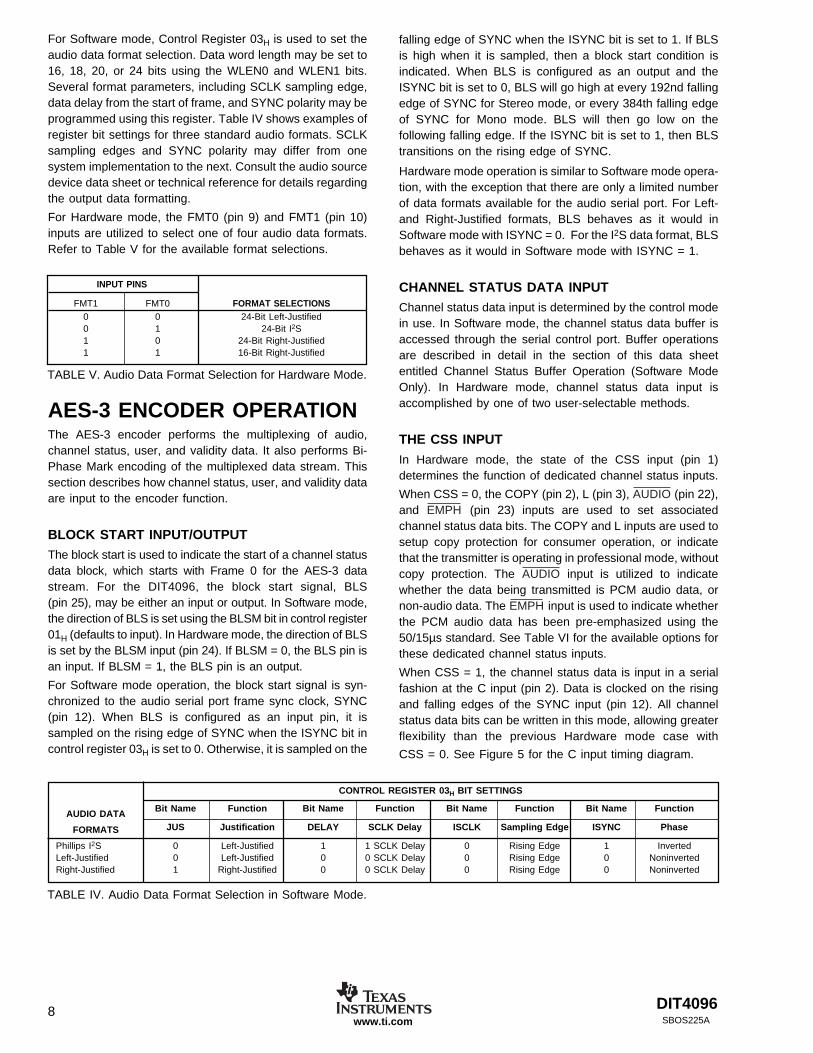
For Software mode, Control Register 03H is used to set theaudio data format selection. Data word length may be set to16, 18, 20, or 24 bits using the WLEN0 and WLEN1 bits.Several format parameters, including SCLK sampling edge,data delay from the start of frame, and SYNC polarity may beprogrammed using this register. Table IV shows examples ofregister bit settings for three standard audio formats. SCLKsampling edges and SYNC polarity may differ from onesystem implementation to the next. Consult the audio sourcedevice data sheet or technical reference for details regardingthe output data formatting.
For Hardware mode, the FMT0 (pin 9) and FMT1 (pin 10)inputs are utilized to select one of four audio data formats.Refer to Table V for the available format selections.
INPUT PINS
FMT1 FMT0 FORMAT SELECTIONS0 0 24-Bit Left-Justified0 1 24-Bit I2S1 0 24-Bit Right-Justified1 1 16-Bit Right-Justified
TABLE V. Audio Data Format Selection for Hardware Mode.
AES-3 ENCODER OPERATIONThe AES-3 encoder performs the multiplexing of audio,channel status, user, and validity data. It also performs Bi-Phase Mark encoding of the multiplexed data stream. Thissection describes how channel status, user, and validity dataare input to the encoder function.
BLOCK START INPUT/OUTPUTThe block start is used to indicate the start of a channel statusdata block, which starts with Frame 0 for the AES-3 datastream. For the DIT4096, the block start signal, BLS(pin 25), may be either an input or output. In Software mode,the direction of BLS is set using the BLSM bit in control register01H (defaults to input). In Hardware mode, the direction of BLSis set by the BLSM input (pin 24). If BLSM = 0, the BLS pin isan input. If BLSM = 1, the BLS pin is an output.
For Software mode operation, the block start signal is syn-chronized to the audio serial port frame sync clock, SYNC(pin 12). When BLS is configured as an input pin, it issampled on the rising edge of SYNC when the ISYNC bit incontrol register 03H is set to 0. Otherwise, it is sampled on the
falling edge of SYNC when the ISYNC bit is set to 1. If BLSis high when it is sampled, then a block start condition isindicated. When BLS is configured as an output and theISYNC bit is set to 0, BLS will go high at every 192nd fallingedge of SYNC for Stereo mode, or every 384th falling edgeof SYNC for Mono mode. BLS will then go low on thefollowing falling edge. If the ISYNC bit is set to 1, then BLStransitions on the rising edge of SYNC.
Hardware mode operation is similar to Software mode opera-tion, with the exception that there are only a limited numberof data formats available for the audio serial port. For Left-and Right-Justified formats, BLS behaves as it would inSoftware mode with ISYNC = 0. For the I2S data format, BLSbehaves as it would in Software mode with ISYNC = 1.
CHANNEL STATUS DATA INPUTChannel status data input is determined by the control modein use. In Software mode, the channel status data buffer isaccessed through the serial control port. Buffer operationsare described in detail in the section of this data sheetentitled Channel Status Buffer Operation (Software ModeOnly). In Hardware mode, channel status data input isaccomplished by one of two user-selectable methods.
THE CSS INPUT
In Hardware mode, the state of the CSS input (pin 1)determines the function of dedicated channel status inputs.
When CSS = 0, the COPY (pin 2), L (pin 3), AUDIO (pin 22),and EMPH (pin 23) inputs are used to set associatedchannel status data bits. The COPY and L inputs are used tosetup copy protection for consumer operation, or indicatethat the transmitter is operating in professional mode, withoutcopy protection. The AUDIO input is utilized to indicatewhether the data being transmitted is PCM audio data, ornon-audio data. The EMPH input is used to indicate whetherthe PCM audio data has been pre-emphasized using the50/15µs standard. See Table VI for the available options forthese dedicated channel status inputs.
When CSS = 1, the channel status data is input in a serialfashion at the C input (pin 2). Data is clocked on the risingand falling edges of the SYNC input (pin 12). All channelstatus data bits can be written in this mode, allowing greaterflexibility than the previous Hardware mode case with
CSS = 0. See Figure 5 for the C input timing diagram.

DIT4096 9SBOS225A www.ti.com
INPUT FUNCTION
COPY Copy Status
L Generation Status
COPY L Status0 0 Consumer Mode, PRO = 0, COPY = 0, L = 00 1 Consumer Mode, PRO = 0, COPY = 0, L = 11 0 Consumer Mode, PRO = 0, COPY = 1, L = 01 1 Professional Mode, PRO = 1, No Copy Protection
AUDIO Audio Data Status
AUDIO Status
0 Digital (or Linear PCM) Audio Data.
1 Non-Audio or Encoded Audio Data.
EMPH Pre-Emphasis Status
EMPH Status
0 Pre-emphasis bits are set to indicate 50/15µs Pre-emphasis has been applied.
1 Pre-emphasis bits are set to indicate that no Pre-emphasis has been applied.
Frame 191 or 383 Frame 0
Block Start
SYNC(1)
BLS(Input)
BLS(Output)
C, U, or VData
NOTE: (1) Assumes ISYNC = 0.
tCUVS tCUVH
Ch BData
Ch AData
Ch BData
Ch AData
192nd or 384thFalling Edge(1)
TABLE VI. Channel Status Data Input for Hardware Mode with CSS = 0.
FIGURE 5. C, U, and V Data Timing.
USER AND VALIDITY DATA INPUTThe user data bits in the AES-3 data stream allow for aconvenient way to transfer user-defined or application spe-cific data to another device containing an AES-3 receiver.The U input (pin 27) is used in both Software and Hardwaremode to input the user data in a serial fashion. Figure 5shows the U input timing diagram.
Validity data is used to indicate that a sample is error-freeaudio data, or that the sample is defective and is not suitable
for further processing. In Software mode, the VAL bit incontrol register 01H is utilized to write the validity data. InHardware mode, the V input (pin 26) is used to input thevalidity data in serial fashion. Refer to Figure 5 for V inputtiming for Hardware Mode.
When VAL or V = 0, this indicates that the audio data is validand suitable for further processing. When VAL or V = 1, then
the audio sample is defective and should not be used.
DIT409610SBOS225Awww.ti.com
LINE DRIVER OUTPUTSThe DIT4096 includes a balanced line driver. The line driveroutputs are TX– (pin 17) and TX+ (pin 18). In Software mode,the line driver input is taken from either the output of the on-chip AES-3 encoder, or from an external AES-3 encodedsource input at RXP (pin 9). The input source is selectedusing the BYPASS bit in control register 01H (defaults to theon-chip AES-3 encoder). In Hardware mode, the line driversource is always the on-chip AES-3 encoder.
The outputs of the line driver will follow the AES-3 encodeddata source in normal operation. During a hardware orsoftware reset, or when the device is in power-down mode,the line driver outputs will be forced to ground. The outputscan also be forced to ground at any time in Software mode
by setting the TXOFF bit to 1 in control register 01H.
CONTROL PORT OPERATION(SOFTWARE MODE ONLY)For Software mode operation, the DIT4096 includes a serialcontrol port, which is used to write and read control registersand the channel status data buffer. Port signals include CS(pin 5), CDIN (pin 4), CDOUT (pin 2), and CCLK (pin 3).
CS is the active low chip select. This signal must be drivenlow in order to write or read control registers and the channelstatus data buffer.
CDIN is the serial data input, while CDOUT serves as theserial data output. The CDOUT pin is a tri-state output, whichis set to a high-impedance state when not performing a Readoperation, or when CS = 1.
CCLK is the data clock for the serial control interface. Datais clocked in at CDIN on the rising edge of CCLK, while datais clocked out at CDOUT on the falling edge of CCLK. Data
is clocked MSB first for both CDIN and CDOUT.
WRITE OPERATION
Figure 6 illustrates the write operation for the control port.You may write one register or buffer address at a time, or usethe auto-increment capability built into the control port toperform block writes. The register or buffer data is precededby a 16-bit header, with the first byte being used to configurecontrol port operation and set the starting register or bufferaddress. The second byte of the header is comprised of“don’t care” bits, which can be set to either 0 or 1 withoutaffecting port operation.
The first byte of the header contains two control bits, R/Wand STEP, followed by a 6-bit address. For write operations,R/W = 0. The STEP bit determines the address step size forthe auto-increment operation. When STEP = 0, the addressis incremented by 1. When STEP = 1, the address isincremented by 2. Incrementing by 1 is useful when writingmultiple control registers in sequence, or when writing both leftand right channel status data in sequence. Incrementing by 2is useful when writing just one channel of status data insequence.
The third byte contains the 8-bit data for the register or bufferaddress designated by the first byte of the header. To write asingle address location, CS is brought high after the leastsignificant bit of the third byte is clocked into the port. For autoincrement mode, CS is kept low to write successive registeror buffer addresses.
Byte 0 Byte 1 Byte 2 Byte 3 Byte N
Register or Buffer DataHeader
Set CS = 1 here to write one register or buffer location. Keep CS = 0 to enable auto-increment mode.
CS
CDIN
CCLK
R/W STEP A5 A4 A3 A2 A1 A0
MSB LSB
BYTE 0:
BYTE DEFINITION
Auto-Increment Address Step Size: 0 = Increment Address by 11 = Increment Address by 2
Register or Buffer Address
Read/Write Control: Set to 1 for Read Operation
Byte 1: All 8 bits are Don’t Care. Set 0 or 1.Bytes 2 through N: 8-Bit Register or Buffer data.
FIGURE 6. Write Operation Format.
DIT4096 11SBOS225A www.ti.com
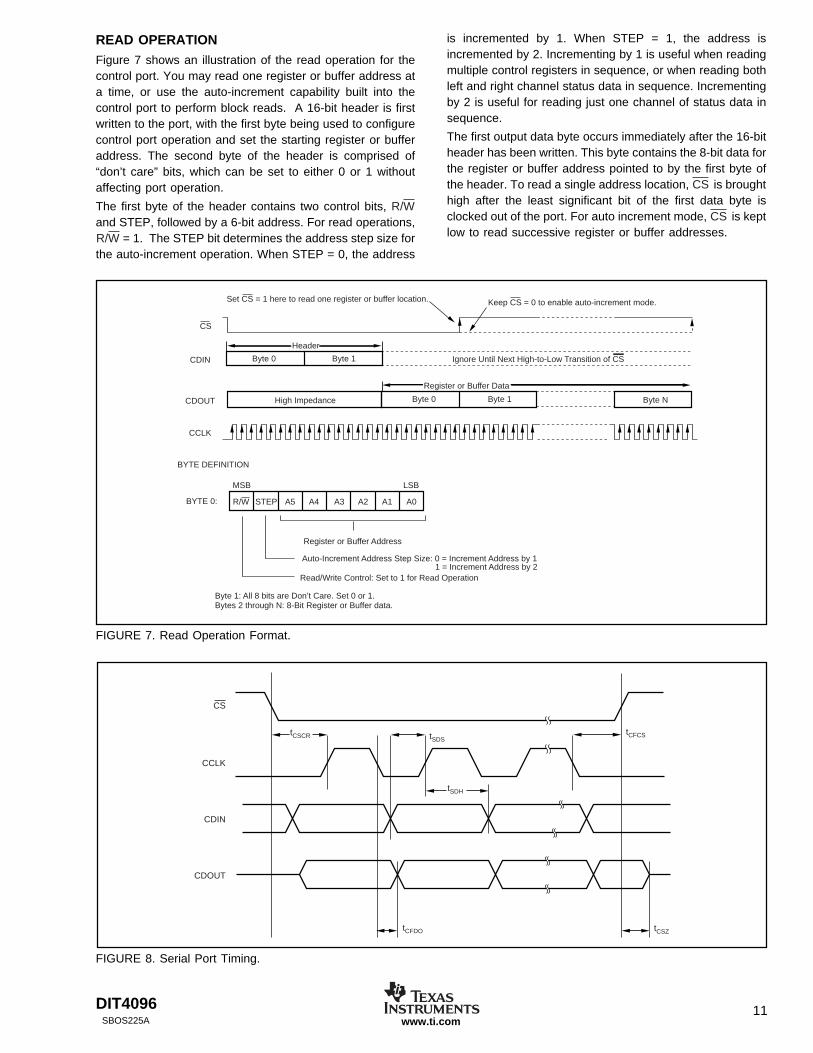
READ OPERATIONFigure 7 shows an illustration of the read operation for thecontrol port. You may read one register or buffer address ata time, or use the auto-increment capability built into thecontrol port to perform block reads. A 16-bit header is firstwritten to the port, with the first byte being used to configurecontrol port operation and set the starting register or bufferaddress. The second byte of the header is comprised of“don’t care” bits, which can be set to either 0 or 1 withoutaffecting port operation.
The first byte of the header contains two control bits, R/Wand STEP, followed by a 6-bit address. For read operations,R/W = 1. The STEP bit determines the address step size forthe auto-increment operation. When STEP = 0, the address
is incremented by 1. When STEP = 1, the address isincremented by 2. Incrementing by 1 is useful when readingmultiple control registers in sequence, or when reading bothleft and right channel status data in sequence. Incrementingby 2 is useful for reading just one channel of status data insequence.
The first output data byte occurs immediately after the 16-bitheader has been written. This byte contains the 8-bit data forthe register or buffer address pointed to by the first byte ofthe header. To read a single address location, CS is broughthigh after the least significant bit of the first data byte isclocked out of the port. For auto increment mode, CS is keptlow to read successive register or buffer addresses.
Byte 0 Byte 1
Byte N
Header
Set CS = 1 here to read one register or buffer location. Keep CS = 0 to enable auto-increment mode.
CS
CDIN
CDOUT
CCLK
R/W STEP A5 A4 A3 A2 A1 A0
MSB LSB
BYTE 0:
BYTE DEFINITION
Auto-Increment Address Step Size: 0 = Increment Address by 11 = Increment Address by 2
Register or Buffer Address
Read/Write Control: Set to 1 for Read Operation
Byte 1: All 8 bits are Don’t Care. Set 0 or 1.Bytes 2 through N: 8-Bit Register or Buffer data.
High Impedance Byte 0 Byte 1
Register or Buffer Data
Ignore Until Next High-to-Low Transition of CS
FIGURE 7. Read Operation Format.
FIGURE 8. Serial Port Timing.
tCSCR tSDS
tSDH
tCFDO tCSZ
tCFCS
CS
CCLK
CDIN
CDOUT
DIT409612SBOS225Awww.ti.com
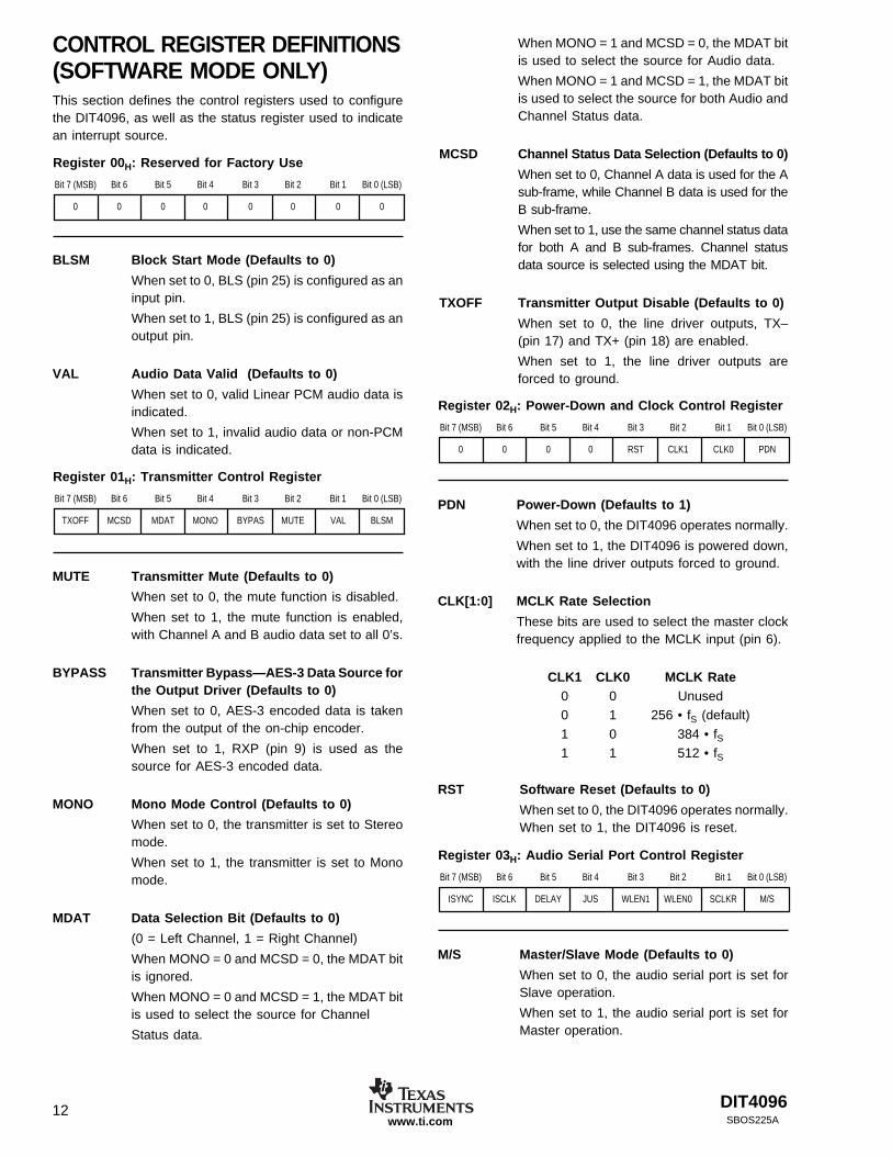
CONTROL REGISTER DEFINITIONS(SOFTWARE MODE ONLY)This section defines the control registers used to configurethe DIT4096, as well as the status register used to indicatean interrupt source.
When MONO = 1 and MCSD = 0, the MDAT bitis used to select the source for Audio data.
When MONO = 1 and MCSD = 1, the MDAT bitis used to select the source for both Audio andChannel Status data.
MCSD Channel Status Data Selection (Defaults to 0)
When set to 0, Channel A data is used for the Asub-frame, while Channel B data is used for theB sub-frame.
When set to 1, use the same channel status datafor both A and B sub-frames. Channel statusdata source is selected using the MDAT bit.
TXOFF Transmitter Output Disable (Defaults to 0)
When set to 0, the line driver outputs, TX–(pin 17) and TX+ (pin 18) are enabled.
When set to 1, the line driver outputs areforced to ground.
MUTE Transmitter Mute (Defaults to 0)
When set to 0, the mute function is disabled.
When set to 1, the mute function is enabled,with Channel A and B audio data set to all 0’s.
BYPASS Transmitter Bypass—AES-3 Data Source forthe Output Driver (Defaults to 0)
When set to 0, AES-3 encoded data is takenfrom the output of the on-chip encoder.
When set to 1, RXP (pin 9) is used as thesource for AES-3 encoded data.
MONO Mono Mode Control (Defaults to 0)
When set to 0, the transmitter is set to Stereomode.
When set to 1, the transmitter is set to Monomode.
MDAT Data Selection Bit (Defaults to 0)
(0 = Left Channel, 1 = Right Channel)
When MONO = 0 and MCSD = 0, the MDAT bitis ignored.
When MONO = 0 and MCSD = 1, the MDAT bitis used to select the source for Channel
Status data.
PDN Power-Down (Defaults to 1)
When set to 0, the DIT4096 operates normally.
When set to 1, the DIT4096 is powered down,with the line driver outputs forced to ground.
CLK[1:0] MCLK Rate Selection
These bits are used to select the master clockfrequency applied to the MCLK input (pin 6).
CLK1 CLK0 MCLK Rate0 0 Unused0 1 256 • fS (default)
1 0 384 • fS1 1 512 • fS
RST Software Reset (Defaults to 0)
When set to 0, the DIT4096 operates normally.When set to 1, the DIT4096 is reset.
M/S Master/Slave Mode (Defaults to 0)
When set to 0, the audio serial port is set forSlave operation.
When set to 1, the audio serial port is set forMaster operation.
BLSM Block Start Mode (Defaults to 0)
When set to 0, BLS (pin 25) is configured as aninput pin.
When set to 1, BLS (pin 25) is configured as anoutput pin.
VAL Audio Data Valid (Defaults to 0)
When set to 0, valid Linear PCM audio data isindicated.
When set to 1, invalid audio data or non-PCMdata is indicated.
Bit 7 (MSB) Bit 6 Bit 5 Bit 4 Bit 3 Bit 2 Bit 1 Bit 0 (LSB)
0 0 0 0 RST CLK1 CLK0 PDN
Register 02H: Power-Down and Clock Control Register
Bit 7 (MSB) Bit 6 Bit 5 Bit 4 Bit 3 Bit 2 Bit 1 Bit 0 (LSB)
ISYNC ISCLK DELAY JUS WLEN1 WLEN0 SCLKR M/S
Register 03H: Audio Serial Port Control Register
Bit 7 (MSB) Bit 6 Bit 5 Bit 4 Bit 3 Bit 2 Bit 1 Bit 0 (LSB)
TXOFF MCSD MDAT MONO BYPAS MUTE VAL BLSM
Register 01H: Transmitter Control Register
Bit 7 (MSB) Bit 6 Bit 5 Bit 4 Bit 3 Bit 2 Bit 1 Bit 0 (LSB)
0 0 0 0 0 0 0 0
Register 00H: Reserved for Factory Use
DIT4096 13SBOS225A www.ti.com
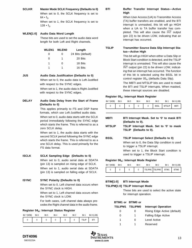
SCLKR Master Mode SCLK Frequency (Defaults to 0)
When set to 0, the SCLK frequency is set to64 • fS.
When set to 1, the SCLK frequency is set to128 • fS.
WLEN[1:0] Audio Data Word Length
These bits are used to set the audio data wordlength for both Left and Right channels.
WLEN1 WLEN0 Length0 0 24 Bits (default)
0 1 20 Bits
1 0 18 Bits
1 1 16 Bits
JUS Audio Data Justification (Defaults to 0)
When set to 0, the audio data is Left-Justified
with respect to the SYNC edges.
When set to 1, the audio data is Right-Justifiedwith respect to the SYNC edges.
DELAY Audio Data Delay from the Start of Frame(Defaults to 0)
This applies primarily to I2S and DSP frameformats, which use Left-Justified audio data.
When set to 0, audio data starts with the SCLKperiod immediately following the SYNC edgewhich starts the frame. This is referred to as azero SCLK delay.
When set to 1, the audio data starts with thesecond SCLK period following the SYNC edgewhich starts the frame. This is referred to as aone SCLK delay. This is used primarily for theI2S data format.
ISCLK SCLK Sampling Edge (Defaults to 0)
When set to 0, audio serial data at SDATA(pin 13) is sampled on rising edge of SCLK.
When set to 1, audio serial data at SDATA(pin 13) is sampled on falling edge of SCLK.
ISYNC SYNC Polarity (Defaults to 0)
When set to 0, Left channel data occurs whenthe SYNC clock is HIGH.
When set to 1, Left channel data occurs whenthe SYNC clock is LOW.
For both cases, Left channel data always pre-cedes the Right channel data in the audio frame.
BTI Buffer Transfer Interrupt Status—ActiveHigh
When User Access (UA) to Transmitter Access(TA) buffer transfers are enabled, and the BTIinterrupt is unmasked, this bit will go HIGHwhen a UA to TA buffer transfer has com-pleted. This will also cause the INT output(pin 22) to be driven LOW, indicating that aninterrupt has occurred.
TSLIP Transmitter Source Data Slip Interrupt Sta-tus—Active High
This bit will go HIGH when either a Data Slip orBlock Start condition is detected, and the TSLIPinterrupt is unmasked. This will also cause theINT output (pin 22) to be driven LOW, indicat-ing that an interrupt has occurred. The functionof this bit is selected using the BSSL bit incontrol register 05H (defaults Data Slip).
The MBTI and MTSLIP bits are used to maskthe BTI and TSLIP interrupts. When masked,these interrupt sources are disabled.
MBTI BTI Interrupt Mask. Set to ‘0’ to mask BTI(Defaults to 0).
MTSLIP TSLIP Interrupt Mask. Set to ‘0’ to maskTSLIP (Defaults to 0).
BSSL TSLIP Interrupt Select (Defaults to 0)
When set to 0, the Data Slip condition is usedto trigger a TSLIP interrupt.
When set to 1, the Block Start condition isused to trigger a TSLIP interrupt.
BTIM[1:0] BTI Interrupt Mode
TSLIPM[1:0] TSLIP Interrupt Mode
These bits are used to select the active statefor interrupt operation.
BTIM1 or BTIM0 or
TSLIPM1 TSLIPM0 Interrupt Operation
0 0 Rising Edge Active (default)
0 1 Falling Edge Active
1 0 Level Active
1 1 Reserved
Bit 7 (MSB) Bit 6 Bit 5 Bit 4 Bit 3 Bit 2 Bit 1 Bit 0 (LSB)
0 0 0 0 0 0 TSLIP BTI
Register 04H: Interrupt Status Register
Bit 7 (MSB) Bit 6 Bit 5 Bit 4 Bit 3 Bit 2 Bit 1 Bit 0 (LSB)
0 0 0 0 0 BSSL MTSLIP MBTI
Register 05H: Interrupt Mask Register
Bit 7 (MSB) Bit 6 Bit 5 Bit 4 Bit 3 Bit 2 Bit 1 Bit 0 (LSB)
0 0 0 0 TSLIPM1 TSLIPM0 BTIM1 BTIM0
Register 06H: Interrupt Mode Register
DIT409614SBOS225Awww.ti.com
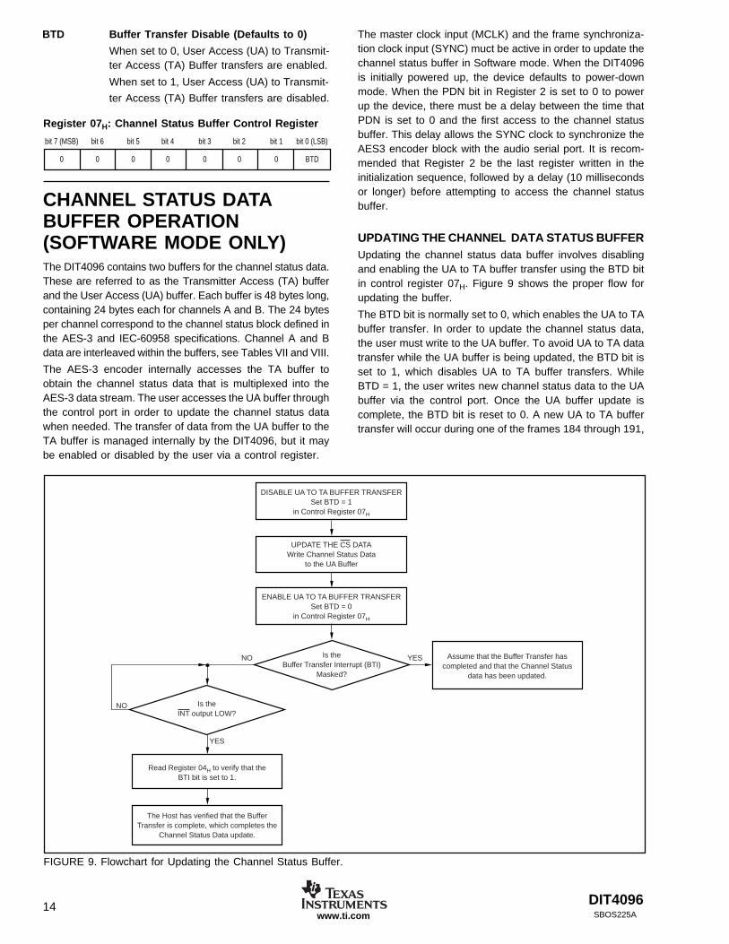
BTD Buffer Transfer Disable (Defaults to 0)
When set to 0, User Access (UA) to Transmit-ter Access (TA) Buffer transfers are enabled.
When set to 1, User Access (UA) to Transmit-
ter Access (TA) Buffer transfers are disabled.
The master clock input (MCLK) and the frame synchroniza-tion clock input (SYNC) muct be active in order to update thechannel status buffer in Software mode. When the DIT4096is initially powered up, the device defaults to power-downmode. When the PDN bit in Register 2 is set to 0 to powerup the device, there must be a delay between the time thatPDN is set to 0 and the first access to the channel statusbuffer. This delay allows the SYNC clock to synchronize theAES3 encoder block with the audio serial port. It is recom-mended that Register 2 be the last register written in theinitialization sequence, followed by a delay (10 millisecondsor longer) before attempting to access the channel statusbuffer.
UPDATING THE CHANNEL DATA STATUS BUFFERUpdating the channel status data buffer involves disablingand enabling the UA to TA buffer transfer using the BTD bitin control register 07H. Figure 9 shows the proper flow forupdating the buffer.
The BTD bit is normally set to 0, which enables the UA to TAbuffer transfer. In order to update the channel status data,the user must write to the UA buffer. To avoid UA to TA datatransfer while the UA buffer is being updated, the BTD bit isset to 1, which disables UA to TA buffer transfers. WhileBTD = 1, the user writes new channel status data to the UAbuffer via the control port. Once the UA buffer update iscomplete, the BTD bit is reset to 0. A new UA to TA buffertransfer will occur during one of the frames 184 through 191,
CHANNEL STATUS DATABUFFER OPERATION(SOFTWARE MODE ONLY)The DIT4096 contains two buffers for the channel status data.These are referred to as the Transmitter Access (TA) bufferand the User Access (UA) buffer. Each buffer is 48 bytes long,containing 24 bytes each for channels A and B. The 24 bytesper channel correspond to the channel status block defined inthe AES-3 and IEC-60958 specifications. Channel A and Bdata are interleaved within the buffers, see Tables VII and VIII.
The AES-3 encoder internally accesses the TA buffer toobtain the channel status data that is multiplexed into theAES-3 data stream. The user accesses the UA buffer throughthe control port in order to update the channel status datawhen needed. The transfer of data from the UA buffer to theTA buffer is managed internally by the DIT4096, but it maybe enabled or disabled by the user via a control register.
DISABLE UA TO TA BUFFER TRANSFERSet BTD = 1
in Control Register 07H
UPDATE THE CS DATAWrite Channel Status Data
to the UA Buffer
ENABLE UA TO TA BUFFER TRANSFERSet BTD = 0
in Control Register 07H
Read Register 04H to verify that theBTI bit is set to 1.
The Host has verified that the BufferTransfer is complete, which completes the
Channel Status Data update.
Assume that the Buffer Transfer hascompleted and that the Channel Status
data has been updated.
Is theBuffer Transfer Interrupt (BTI)
Masked?
Is theINT output LOW?
YES
YES
NO
NO
FIGURE 9. Flowchart for Updating the Channel Status Buffer.
bit 7 (MSB) bit 6 bit 5 bit 4 bit 3 bit 2 bit 1 bit 0 (LSB)
0 0 0 0 0 0 0 BTD
Register 07H: Channel Status Buffer Control Register
DIT4096 15SBOS225A www.ti.com
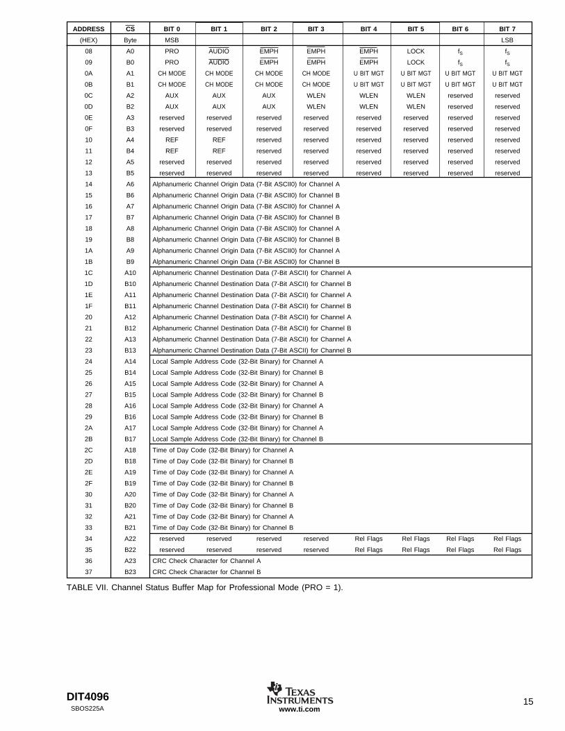
ADDRESS CS BIT 0 BIT 1 BIT 2 BIT 3 BIT 4 BIT 5 BIT 6 BIT 7
(HEX) Byte MSB LSB
08 A0 PRO AUDIO EMPH EMPH EMPH LOCK fS fS
09 B0 PRO AUDIO EMPH EMPH EMPH LOCK fS fS
0A A1 CH MODE CH MODE CH MODE CH MODE U BIT MGT U BIT MGT U BIT MGT U BIT MGT
0B B1 CH MODE CH MODE CH MODE CH MODE U BIT MGT U BIT MGT U BIT MGT U BIT MGT
0C A2 AUX AUX AUX WLEN WLEN WLEN reserved reserved
0D B2 AUX AUX AUX WLEN WLEN WLEN reserved reserved
0E A3 reserved reserved reserved reserved reserved reserved reserved reserved
0F B3 reserved reserved reserved reserved reserved reserved reserved reserved
10 A4 REF REF reserved reserved reserved reserved reserved reserved
11 B4 REF REF reserved reserved reserved reserved reserved reserved
12 A5 reserved reserved reserved reserved reserved reserved reserved reserved
13 B5 reserved reserved reserved reserved reserved reserved reserved reserved
14 A6 Alphanumeric Channel Origin Data (7-Bit ASCII0) for Channel A
15 B6 Alphanumeric Channel Origin Data (7-Bit ASCII0) for Channel B
16 A7 Alphanumeric Channel Origin Data (7-Bit ASCII0) for Channel A
17 B7 Alphanumeric Channel Origin Data (7-Bit ASCII0) for Channel B
18 A8 Alphanumeric Channel Origin Data (7-Bit ASCII0) for Channel A
19 B8 Alphanumeric Channel Origin Data (7-Bit ASCII0) for Channel B
1A A9 Alphanumeric Channel Origin Data (7-Bit ASCII0) for Channel A
1B B9 Alphanumeric Channel Origin Data (7-Bit ASCII0) for Channel B
1C A10 Alphanumeric Channel Destination Data (7-Bit ASCII) for Channel A
1D B10 Alphanumeric Channel Destination Data (7-Bit ASCII) for Channel B
1E A11 Alphanumeric Channel Destination Data (7-Bit ASCII) for Channel A
1F B11 Alphanumeric Channel Destination Data (7-Bit ASCII) for Channel B
20 A12 Alphanumeric Channel Destination Data (7-Bit ASCII) for Channel A
21 B12 Alphanumeric Channel Destination Data (7-Bit ASCII) for Channel B
22 A13 Alphanumeric Channel Destination Data (7-Bit ASCII) for Channel A
23 B13 Alphanumeric Channel Destination Data (7-Bit ASCII) for Channel B
24 A14 Local Sample Address Code (32-Bit Binary) for Channel A
25 B14 Local Sample Address Code (32-Bit Binary) for Channel B
26 A15 Local Sample Address Code (32-Bit Binary) for Channel A
27 B15 Local Sample Address Code (32-Bit Binary) for Channel B
28 A16 Local Sample Address Code (32-Bit Binary) for Channel A
29 B16 Local Sample Address Code (32-Bit Binary) for Channel B
2A A17 Local Sample Address Code (32-Bit Binary) for Channel A
2B B17 Local Sample Address Code (32-Bit Binary) for Channel B
2C A18 Time of Day Code (32-Bit Binary) for Channel A
2D B18 Time of Day Code (32-Bit Binary) for Channel B
2E A19 Time of Day Code (32-Bit Binary) for Channel A
2F B19 Time of Day Code (32-Bit Binary) for Channel B
30 A20 Time of Day Code (32-Bit Binary) for Channel A
31 B20 Time of Day Code (32-Bit Binary) for Channel B
32 A21 Time of Day Code (32-Bit Binary) for Channel A
33 B21 Time of Day Code (32-Bit Binary) for Channel B
34 A22 reserved reserved reserved reserved Rel Flags Rel Flags Rel Flags Rel Flags
35 B22 reserved reserved reserved reserved Rel Flags Rel Flags Rel Flags Rel Flags
36 A23 CRC Check Character for Channel A
37 B23 CRC Check Character for Channel B
TABLE VII. Channel Status Buffer Map for Professional Mode (PRO = 1).

DIT409616SBOS225Awww.ti.com
whichever is the first frame to occur after the BTD bit is resetto 0. Once the UA to TA buffer transfer is completed, the buffertransfer interrupt (BTI) will occur, as long as it is unmasked.
The transmitter will ignore any attempt to access the UAbuffer during a UA to TA buffer transfer. In addition, the BTDbit may be set to 1 to stop a UA to TA buffer transfer that maybe in progress, if so desired.
CHANNEL STATUS BUFFER MAPThe channel status buffer is organized in accordance with theAES-3 and IEC-60958 standards. See Table VII for the memorymap for the UA channel status data buffer for Professional mode.Table VIII shows the memory map for the UA channel status databuffer for Consumer mode.
ADDRESS CS BIT 0 BIT 1 BIT 2 BIT 3 BIT 4 BIT 5 BIT 6 BIT 7
(HEX) Byte MSB LSB
8 A0 PRO = 0 AUDIO COPY EMPH EMPH EMPH MODE MODE09 B0 PRO = 0 AUDIO COPY EMPH EMPH EMPH MODE MODE0A A1 CAT CODE CAT CODE CAT CODE CAT CODE CAT CODE CAT CODE CAT CODE L0B B1 CAT CODE CAT CODE CAT CODE CAT CODE CAT CODE CAT CODE CAT CODE L0C A2 SOURCE SOURCE SOURCE SOURCE CH NUM CH NUM CH NUM CH NUM0D B2 SOURCE SOURCE SOURCE SOURCE CH NUM CH NUM CH NUM CH NUM0E A3 fS fS fS fS CLK ACC CLK ACC reserved reserved0F B3 fS fS fS fS CLK ACC CLK ACC reserved reserved10 A4 reserved reserved reserved reserved reserved reserved reserved reserved11 B4 reserved reserved reserved reserved reserved reserved reserved reserved12 A5 reserved reserved reserved reserved reserved reserved reserved reserved13 B5 reserved reserved reserved reserved reserved reserved reserved reserved14 A6 reserved reserved reserved reserved reserved reserved reserved reserved15 B6 reserved reserved reserved reserved reserved reserved reserved reserved16 A7 reserved reserved reserved reserved reserved reserved reserved reserved17 B7 reserved reserved reserved reserved reserved reserved reserved reserved18 A8 reserved reserved reserved reserved reserved reserved reserved reserved19 B8 reserved reserved reserved reserved reserved reserved reserved reserved1A A9 reserved reserved reserved reserved reserved reserved reserved reserved1B B9 reserved reserved reserved reserved reserved reserved reserved reserved1C A10 reserved reserved reserved reserved reserved reserved reserved reserved1D B10 reserved reserved reserved reserved reserved reserved reserved reserved1E A11 reserved reserved reserved reserved reserved reserved reserved reserved1F B11 reserved reserved reserved reserved reserved reserved reserved reserved20 A12 reserved reserved reserved reserved reserved reserved reserved reserved21 B12 reserved reserved reserved reserved reserved reserved reserved reserved22 A13 reserved reserved reserved reserved reserved reserved reserved reserved23 B13 reserved reserved reserved reserved reserved reserved reserved reserved24 A14 reserved reserved reserved reserved reserved reserved reserved reserved25 B14 reserved reserved reserved reserved reserved reserved reserved reserved26 A15 reserved reserved reserved reserved reserved reserved reserved reserved27 B15 reserved reserved reserved reserved reserved reserved reserved reserved28 A16 reserved reserved reserved reserved reserved reserved reserved reserved29 B16 reserved reserved reserved reserved reserved reserved reserved reserved2A A17 reserved reserved reserved reserved reserved reserved reserved reserved2B B17 reserved reserved reserved reserved reserved reserved reserved reserved2C A18 reserved reserved reserved reserved reserved reserved reserved reserved2D B18 reserved reserved reserved reserved reserved reserved reserved reserved2E A19 reserved reserved reserved reserved reserved reserved reserved reserved2F B19 reserved reserved reserved reserved reserved reserved reserved reserved30 A20 reserved reserved reserved reserved reserved reserved reserved reserved31 B20 reserved reserved reserved reserved reserved reserved reserved reserved32 A21 reserved reserved reserved reserved reserved reserved reserved reserved33 B21 reserved reserved reserved reserved reserved reserved reserved reserved34 A22 reserved reserved reserved reserved reserved reserved reserved reserved35 B22 reserved reserved reserved reserved reserved reserved reserved reserved36 A23 reserved reserved reserved reserved reserved reserved reserved reserved37 B23 reserved reserved reserved reserved reserved reserved reserved reserved
TABLE VIII. Channel Status Buffer for Consumer Mode (PRO = 0).
INTERRUPT SOURCES(SOFTWARE MODE ONLY)The DIT4096 can be programmed to generate interrupts forup to three predefined conditions. The interrupt output, INT(pin 22), is set low when a valid interrupt occurs. The interruptstatus register, 04H, is then read to determine the source ofthe interrupt. Status register bits and the INT output pinremain active until the status register is read. Once read,status bits are cleared and the INT pin is pulled high by anexternal pull-up resistor to VIO.
Interrupts may be masked using control register 05H. Whenmasked, the interrupt mechanism associated with a particular
status bit is disabled.

DIT4096 17SBOS225A www.ti.com
CHANNEL STATUS BUFFER TRANSFER INTERRUPTThis interrupt occurs when a channel status buffer transferhas been completed. This interrupt may be used by the hostto trigger an event to occur after a channel status bufferupdate. The BTI bit in status register 04H is used to indicatethe occurrence of the buffer transfer. The BTI bit, like all otherstatus bits, is active high and remains set until the statusregister is read.
DATA SLIP AND BLOCK START INTERRUPTS
Unlike the BTI interrupt, which has only one function, the TSLIPinterrupt can be set to one of two modes. This is accomplishedusing the BSSL bit in control register 05H. When BSSL = 0, theTSLIP interrupt is set to indicate a data slip condition. WhenBSSL = 1, the TSLIP interrupt is set to indicate a block startcondition. The TSLIP bit, like all other status bits, is active highand remains set until the status register is read.
A data slip condition may occur in cases where the master clock,MCLK (pin 6), is asynchronous to the audio data source. WhenBSSL = 0, the TSLIP bit will be set to 1 every time a data sampleis dropped or repeated.
FIGURE 10. Typical Circuit Configuration, Software Mode.
TX+
TX–
VIO
DGND
VDD
DGND
18
17
7
8
19
16
RXP
SCLK
SYNC
SDATA
CS
CCLK
CDIN
CDOUT
INT
BLS
U
RST
MCLK
MODE
9
11
12
13
5
3
4
2
22
25
27
15
6
28
DIT4096
Digital AudioSource
(A/D Converter,DSP)
From AES-3Encoded Data
Source(Optional)
µP or DSP
Audio MasterClock
C1
C2
+2.7V to VDD
+5V C1 = C2 = 0.1µF to 1µF
Cable orFiber Optics
OutputCircuit
(See Figs. 12-14)
VIO
10kΩ
A block start condition occurs when a block start signal isgenerated either internally by the DIT4096, or when anexternal block start is received at the BLS input (pin 25).
APPLICATIONS INFORMATIONThis section provides practical information pertinent fordesigning the DIT4096 into a target application. Circuitschematics are provided as needed.
TYPICAL APPLICATION DIAGRAMS
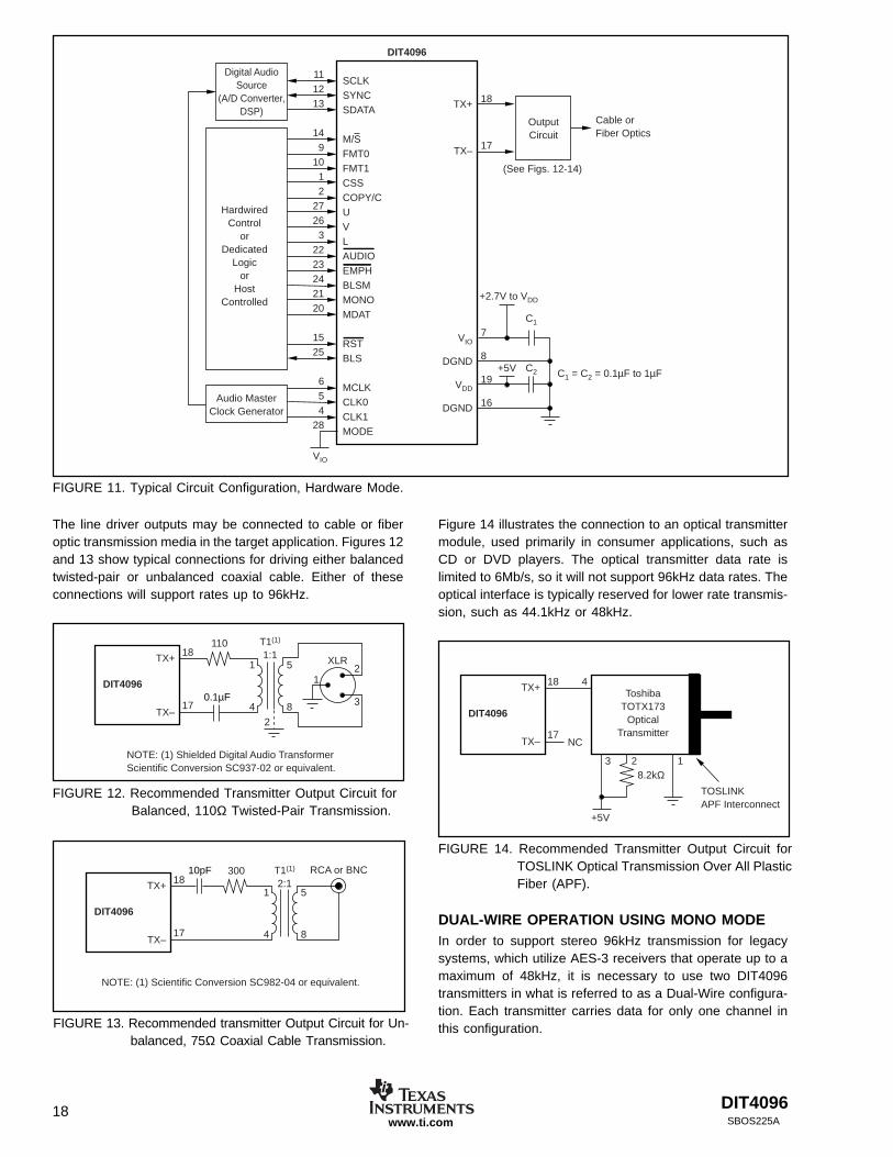
Figures 10 and 11 illustrate the typical application schemat-ics for the DIT4096 when used in Software and Hardwaremodes. Figure 10 shows a typical Software mode applica-tion, where a microprocessor or DSP interface is used tocommunicate with the DIT4096 via the serial control port.See Figure 11 for a typical Hardware mode configuration,where the control pins are either hardwired or driven bydigital logic in a stand-alone application.
The recommended component values for power-supplybypass capacitors are shown in Figures 10 and 11. Thesecapacitors should be located as close to the DIT4096power-supply pins as physically possible.
DIT409618SBOS225Awww.ti.com
DIT4096
TX+
TX–
181
4
5 2
2
1
38
110
17
T1(1)
1:1
NOTE: (1) Shielded Digital Audio TransformerScientific Conversion SC937-02 or equivalent.
XLR
0.1µF
FIGURE 12. Recommended Transmitter Output Circuit forBalanced, 110Ω Twisted-Pair Transmission.
DIT4096
TX+
TX–
181
4
5
8
300
17
RCA or BNCT1(1)
2:1
NOTE: (1) Scientific Conversion SC982-04 or equivalent.
10pF
FIGURE 13. Recommended transmitter Output Circuit for Un-balanced, 75Ω Coaxial Cable Transmission.
DIT4096
TX+
TX–
18
17
3
4
2 1
ToshibaTOTX173
OpticalTransmitter
TOSLINKAPF Interconnect
NC
+5V
8.2kΩ
FIGURE 14. Recommended Transmitter Output Circuit forTOSLINK Optical Transmission Over All PlasticFiber (APF).
TX+
TX–
VIO
DGND
VDD
DGND
18
17
7
8
19
16
SCLKSYNCSDATA
M/SFMT0FMT1CSSCOPY/CUVLAUDIOEMPHBLSMMONOMDAT
RSTBLS
MCLKCLK0CLK1MODE
111213
149
1012
2726
32223242120
1525
654
28
DIT4096
Digital AudioSource
(A/D Converter,DSP)
HardwiredControl
orDedicated
Logicor
HostControlled
Audio MasterClock Generator
C1
C2
+2.7V to VDD
VIO
+5V C1 = C2 = 0.1µF to 1µF
Cable orFiber Optics
OutputCircuit
(See Figs. 12-14)
FIGURE 11. Typical Circuit Configuration, Hardware Mode.
The line driver outputs may be connected to cable or fiberoptic transmission media in the target application. Figures 12and 13 show typical connections for driving either balancedtwisted-pair or unbalanced coaxial cable. Either of theseconnections will support rates up to 96kHz.
Figure 14 illustrates the connection to an optical transmittermodule, used primarily in consumer applications, such asCD or DVD players. The optical transmitter data rate islimited to 6Mb/s, so it will not support 96kHz data rates. Theoptical interface is typically reserved for lower rate transmis-sion, such as 44.1kHz or 48kHz.
DUAL-WIRE OPERATION USING MONO MODEIn order to support stereo 96kHz transmission for legacysystems, which utilize AES-3 receivers that operate up to amaximum of 48kHz, it is necessary to use two DIT4096transmitters in what is referred to as a Dual-Wire configura-tion. Each transmitter carries data for only one channel inthis configuration.
DIT4096 19SBOS225A www.ti.com
INPUT FUNCTION
MONO Stereo/Mono Mode Selection
MONO Status0 Stereo Mode1 Mono Mode
MDAT Mono Mode Audio and Channel Status Data Selection
MDAT Status
0 Source is Left Channel for Audio data, and Channel A for CS data.
1 Source is Right Channel for Audio data, and Channel B for CS data.
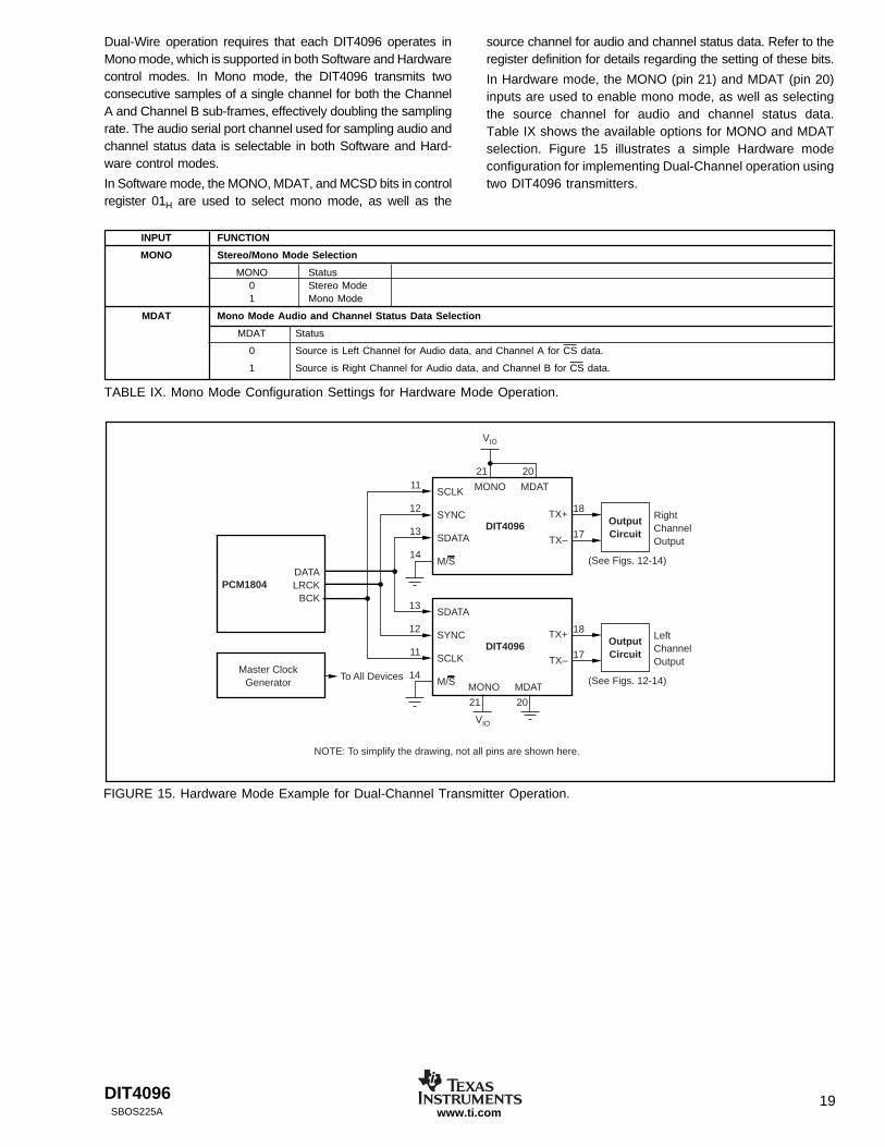
TABLE IX. Mono Mode Configuration Settings for Hardware Mode Operation.
Dual-Wire operation requires that each DIT4096 operates inMono mode, which is supported in both Software and Hardwarecontrol modes. In Mono mode, the DIT4096 transmits twoconsecutive samples of a single channel for both the ChannelA and Channel B sub-frames, effectively doubling the samplingrate. The audio serial port channel used for sampling audio andchannel status data is selectable in both Software and Hard-ware control modes.
In Software mode, the MONO, MDAT, and MCSD bits in controlregister 01H are used to select mono mode, as well as the
source channel for audio and channel status data. Refer to theregister definition for details regarding the setting of these bits.
In Hardware mode, the MONO (pin 21) and MDAT (pin 20)inputs are used to enable mono mode, as well as selectingthe source channel for audio and channel status data.Table IX shows the available options for MONO and MDATselection. Figure 15 illustrates a simple Hardware modeconfiguration for implementing Dual-Channel operation usingtwo DIT4096 transmitters.
SCLK
SYNC
SDATA
M/S
11
12
13
14
13
12
11
14
TX+
TX–
RightChannelOutput
OutputCircuit
(See Figs. 12-14)
SDATA
SYNC
SCLK
M/S
TX+
TX–
LeftChannelOutput
OutputCircuit
(See Figs. 12-14)
DIT4096
DIT4096
PCM1804DATALRCK
BCK
Master ClockGenerator
To All Devices
18
17
18
17
VIO
21 20
MONO MDAT
MONO MDAT
VIO
21 20
NOTE: To simplify the drawing, not all pins are shown here.
FIGURE 15. Hardware Mode Example for Dual-Channel Transmitter Operation.

PACKAGE OPTION ADDENDUM
www.ti.com 10-Dec-2020
Addendum-Page 1
PACKAGING INFORMATION
Orderable Device Status(1)
Package Type PackageDrawing
Pins PackageQty
Eco Plan(2)
Lead finish/Ball material
(6)
MSL Peak Temp(3)
Op Temp (°C) Device Marking(4/5)
Samples
DIT4096IPW ACTIVE TSSOP PW 28 50 RoHS & Green NIPDAU Level-1-260C-UNLIM -40 to 85 DIT4096I
DIT4096IPWR ACTIVE TSSOP PW 28 2000 RoHS & Green NIPDAU Level-1-260C-UNLIM -40 to 85 DIT4096I
(1) The marketing status values are defined as follows:ACTIVE: Product device recommended for new designs.LIFEBUY: TI has announced that the device will be discontinued, and a lifetime-buy period is in effect.NRND: Not recommended for new designs. Device is in production to support existing customers, but TI does not recommend using this part in a new design.PREVIEW: Device has been announced but is not in production. Samples may or may not be available.OBSOLETE: TI has discontinued the production of the device.
(2) RoHS: TI defines "RoHS" to mean semiconductor products that are compliant with the current EU RoHS requirements for all 10 RoHS substances, including the requirement that RoHS substancedo not exceed 0.1% by weight in homogeneous materials. Where designed to be soldered at high temperatures, "RoHS" products are suitable for use in specified lead-free processes. TI mayreference these types of products as "Pb-Free".RoHS Exempt: TI defines "RoHS Exempt" to mean products that contain lead but are compliant with EU RoHS pursuant to a specific EU RoHS exemption.Green: TI defines "Green" to mean the content of Chlorine (Cl) and Bromine (Br) based flame retardants meet JS709B low halogen requirements of <=1000ppm threshold. Antimony trioxide basedflame retardants must also meet the <=1000ppm threshold requirement.
(3) MSL, Peak Temp. - The Moisture Sensitivity Level rating according to the JEDEC industry standard classifications, and peak solder temperature.
(4) There may be additional marking, which relates to the logo, the lot trace code information, or the environmental category on the device.
(5) Multiple Device Markings will be inside parentheses. Only one Device Marking contained in parentheses and separated by a "~" will appear on a device. If a line is indented then it is a continuationof the previous line and the two combined represent the entire Device Marking for that device.
(6) Lead finish/Ball material - Orderable Devices may have multiple material finish options. Finish options are separated by a vertical ruled line. Lead finish/Ball material values may wrap to twolines if the finish value exceeds the maximum column width.
Important Information and Disclaimer:The information provided on this page represents TI's knowledge and belief as of the date that it is provided. TI bases its knowledge and belief on informationprovided by third parties, and makes no representation or warranty as to the accuracy of such information. Efforts are underway to better integrate information from third parties. TI has taken andcontinues to take reasonable steps to provide representative and accurate information but may not have conducted destructive testing or chemical analysis on incoming materials and chemicals.TI and TI suppliers consider certain information to be proprietary, and thus CAS numbers and other limited information may not be available for release.
In no event shall TI's liability arising out of such information exceed the total purchase price of the TI part(s) at issue in this document sold by TI to Customer on an annual basis.
PACKAGE OPTION ADDENDUM
www.ti.com 10-Dec-2020
Addendum-Page 2
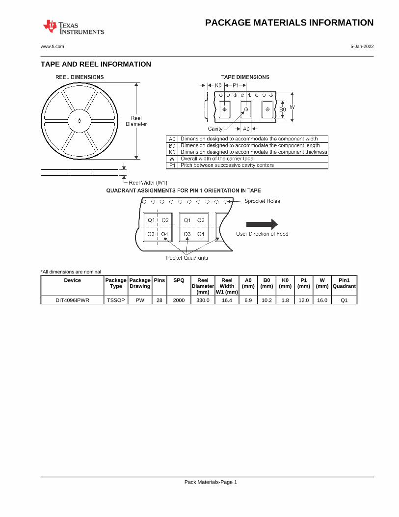
TAPE AND REEL INFORMATION
*All dimensions are nominal
Device PackageType
PackageDrawing
Pins SPQ ReelDiameter
(mm)
ReelWidth
W1 (mm)
A0(mm)
B0(mm)
K0(mm)
P1(mm)
W(mm)
Pin1Quadrant
DIT4096IPWR TSSOP PW 28 2000 330.0 16.4 6.9 10.2 1.8 12.0 16.0 Q1
PACKAGE MATERIALS INFORMATION
www.ti.com 5-Jan-2022
Pack Materials-Page 1
*All dimensions are nominal
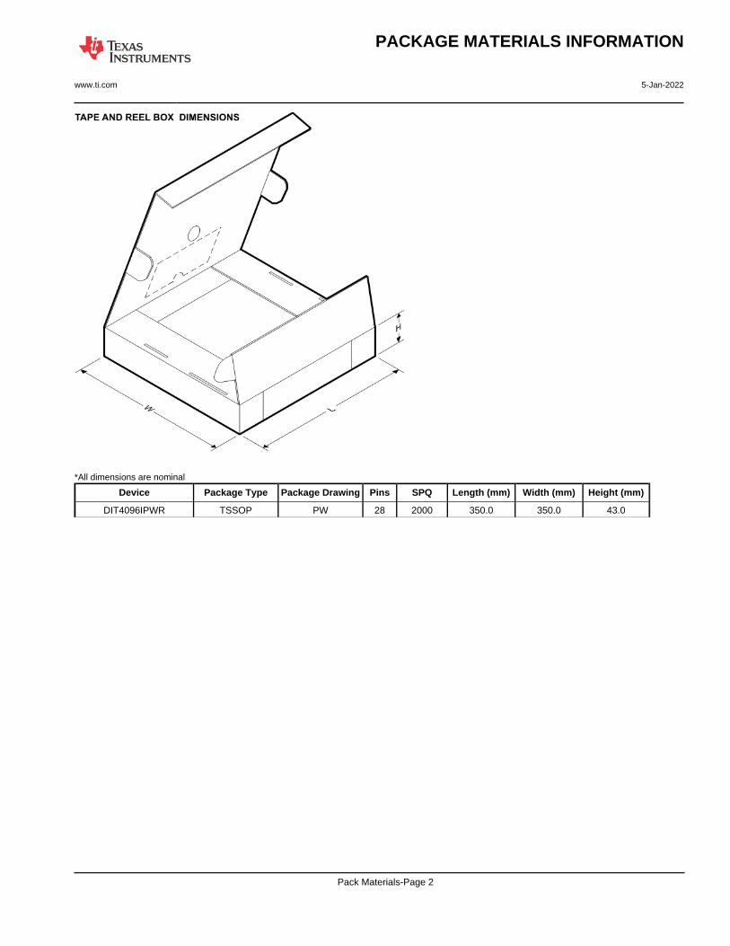
Device Package Type Package Drawing Pins SPQ Length (mm) Width (mm) Height (mm)
DIT4096IPWR TSSOP PW 28 2000 350.0 350.0 43.0
PACKAGE MATERIALS INFORMATION
www.ti.com 5-Jan-2022
Pack Materials-Page 2
TUBE
*All dimensions are nominal
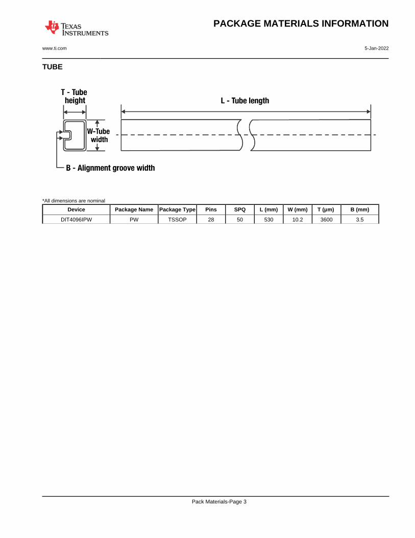
Device Package Name Package Type Pins SPQ L (mm) W (mm) T (µm) B (mm)
DIT4096IPW PW TSSOP 28 50 530 10.2 3600 3.5
PACKAGE MATERIALS INFORMATION
www.ti.com 5-Jan-2022
Pack Materials-Page 3

IMPORTANT NOTICE AND DISCLAIMERTI PROVIDES TECHNICAL AND RELIABILITY DATA (INCLUDING DATA SHEETS), DESIGN RESOURCES (INCLUDING REFERENCE DESIGNS), APPLICATION OR OTHER DESIGN ADVICE, WEB TOOLS, SAFETY INFORMATION, AND OTHER RESOURCES “AS IS” AND WITH ALL FAULTS, AND DISCLAIMS ALL WARRANTIES, EXPRESS AND IMPLIED, INCLUDING WITHOUT LIMITATION ANY IMPLIED WARRANTIES OF MERCHANTABILITY, FITNESS FOR A PARTICULAR PURPOSE OR NON-INFRINGEMENT OF THIRD PARTY INTELLECTUAL PROPERTY RIGHTS.These resources are intended for skilled developers designing with TI products. You are solely responsible for (1) selecting the appropriate TI products for your application, (2) designing, validating and testing your application, and (3) ensuring your application meets applicable standards, and any other safety, security, regulatory or other requirements.These resources are subject to change without notice. TI grants you permission to use these resources only for development of an application that uses the TI products described in the resource. Other reproduction and display of these resources is prohibited. No license is granted to any other TI intellectual property right or to any third party intellectual property right. TI disclaims responsibility for, and you will fully indemnify TI and its representatives against, any claims, damages, costs, losses, and liabilities arising out of your use of these resources.TI’s products are provided subject to TI’s Terms of Sale or other applicable terms available either on ti.com or provided in conjunction with such TI products. TI’s provision of these resources does not expand or otherwise alter TI’s applicable warranties or warranty disclaimers for TI products.TI objects to and rejects any additional or different terms you may have proposed. IMPORTANT NOTICE
Mailing Address: Texas Instruments, Post Office Box 655303, Dallas, Texas 75265Copyright © 2022, Texas Instruments Incorporated