96-W/180-W Peak Dual Interleaved Buck Converter Reference ...
14
1 TIDT035 – November 2018 Submit Documentation Feedback Copyright © 2018, Texas Instruments Incorporated 96-W/180-W Peak Dual Interleaved Buck Converter Reference Design for Space Constrained Applications Test Report: PMP30464 96-W/180-W Peak Dual Interleaved Buck Converter Reference Design for Space Constrained Applications Description The PMP30464 is a dual, interleaved buck converter reference design, which covers an input voltage range of 17.0 V to 60.0 V. The output voltage is 12.0 V with a maximum load current of 15.0 A. The design has been space optimized and supports an average load current of 8.0 A. An IMPORTANT NOTICE at the end of this TI reference design addresses authorized use, intellectual property matters and other important disclaimers and information.
Transcript of 96-W/180-W Peak Dual Interleaved Buck Converter Reference ...

1TIDT035–November 2018Submit Documentation Feedback
Copyright © 2018, Texas Instruments Incorporated
96-W/180-W Peak Dual Interleaved Buck Converter Reference Design forSpace Constrained Applications
Test Report: PMP3046496-W/180-W Peak Dual Interleaved Buck ConverterReference Design for Space Constrained Applications
DescriptionThe PMP30464 is a dual, interleaved buck converter reference design, which covers an input voltage range of17.0 V to 60.0 V. The output voltage is 12.0 V with a maximum load current of 15.0 A. The design has beenspace optimized and supports an average load current of 8.0 A.
An IMPORTANT NOTICE at the end of this TI reference design addresses authorized use, intellectual property matters and otherimportant disclaimers and information.

Test Prerequisites www.ti.com
2 TIDT035–November 2018Submit Documentation Feedback
Copyright © 2018, Texas Instruments Incorporated
96-W/180-W Peak Dual Interleaved Buck Converter Reference Design forSpace Constrained Applications
1 Test Prerequisites
1.1 Voltage and Current Requirements
Table 1. Voltage and Current Requirements
PARAMETER SPECIFICATIONSVIN 17V - 40V, 60V peakVOUT 12.0VIOUT 8A avg., 15A peakNominal switchingfrequency 300kHz

www.ti.com Testing and Results
3TIDT035–November 2018Submit Documentation Feedback
Copyright © 2018, Texas Instruments Incorporated
96-W/180-W Peak Dual Interleaved Buck Converter Reference Design for SpaceConstrained Applications
2 Testing and Results
2.1 Efficiency Graphs
Figure 1. Efficiency at 20.0V, 30.0V and 40.0V in
Voltage [V] Current [A] Power [W] Voltage [V] Current [A] Power [W] Losses [W] Efficiency [%]19.963 6.214 124.050 12.025 9.983 120.046 4.005 96.820.031 4.971 99.574 12.026 8.022 96.473 3.102 96.920.190 3.702 74.743 12.028 6.025 72.466 2.278 97.020.204 2.476 50.025 12.030 4.018 48.337 1.689 96.620.354 1.261 25.666 12.032 2.026 24.377 1.290 95.0
Voltage [V] Current [A] Power [W] Voltage [V] Current [A] Power [W] Losses [W] Efficiency [%]30.055 4.170 125.329 12.022 9.980 119.980 5.350 95.730.163 3.337 100.654 12.023 8.020 96.424 4.229 95.830.191 2.505 75.628 12.025 6.024 72.439 3.190 95.830.203 1.679 50.711 12.028 4.017 48.316 2.394 95.330.299 0.869 26.324 12.031 2.026 24.375 1.949 92.6
Voltage [V] Current [A] Power [W] Voltage [V] Current [A] Power [W] Losses [W] Efficiency [%]39.930 3.165 126.378 12.020 9.977 119.924 6.455 94.940.070 2.535 101.577 12.022 8.017 96.380 5.197 94.940.080 1.907 76.433 12.024 6.022 72.409 4.024 94.7

Testing and Results www.ti.com
4 TIDT035–November 2018Submit Documentation Feedback
Copyright © 2018, Texas Instruments Incorporated
96-W/180-W Peak Dual Interleaved Buck Converter Reference Design forSpace Constrained Applications
40.100 1.281 51.368 12.028 4.015 48.292 3.076 94.040.230 0.669 26.926 12.030 2.025 24.361 2.565 90.5
2.2 Load Regulation
Figure 2. Load regulation at 20.0V, 30.0V and 40.0V in

www.ti.com Testing and Results
5TIDT035–November 2018Submit Documentation Feedback
Copyright © 2018, Texas Instruments Incorporated
96-W/180-W Peak Dual Interleaved Buck Converter Reference Design forSpace Constrained Applications
2.3 Thermal Images
Figure 3. Thermal image of the PCB's top side at 30.0V in and 8.0A load current. For a higher averageload current it is recommended to use more cooling area and a copper thickness of 2oz or more.

Testing and Results www.ti.com
6 TIDT035–November 2018Submit Documentation Feedback
Copyright © 2018, Texas Instruments Incorporated
96-W/180-W Peak Dual Interleaved Buck Converter Reference Design forSpace Constrained Applications
Figure 4. Thermal image of the PCB's bottom side at 30.0V in and 8.0A load current. For a higher averageload current it is recommended to use more cooling area and a copper thickness of 2oz or more.
2.4 DimensionsTotal board size: 88 mm x 50 mm (components cover about 58 mm x 37.3 mm)

www.ti.com Waveforms
7TIDT035–November 2018Submit Documentation Feedback
Copyright © 2018, Texas Instruments Incorporated
96-W/180-W Peak Dual Interleaved Buck Converter Reference Design forSpace Constrained Applications
3 Waveforms
3.1 Switching
Figure 5. Switching node of Q3 and Q4 at 60.0V in and 15.0A load current.
• Ch2: Switching node of Q3 and Q4 [scale: 20.0V/div, 2.0us/div]
Waveforms www.ti.com
8 TIDT035–November 2018Submit Documentation Feedback
Copyright © 2018, Texas Instruments Incorporated
96-W/180-W Peak Dual Interleaved Buck Converter Reference Design forSpace Constrained Applications
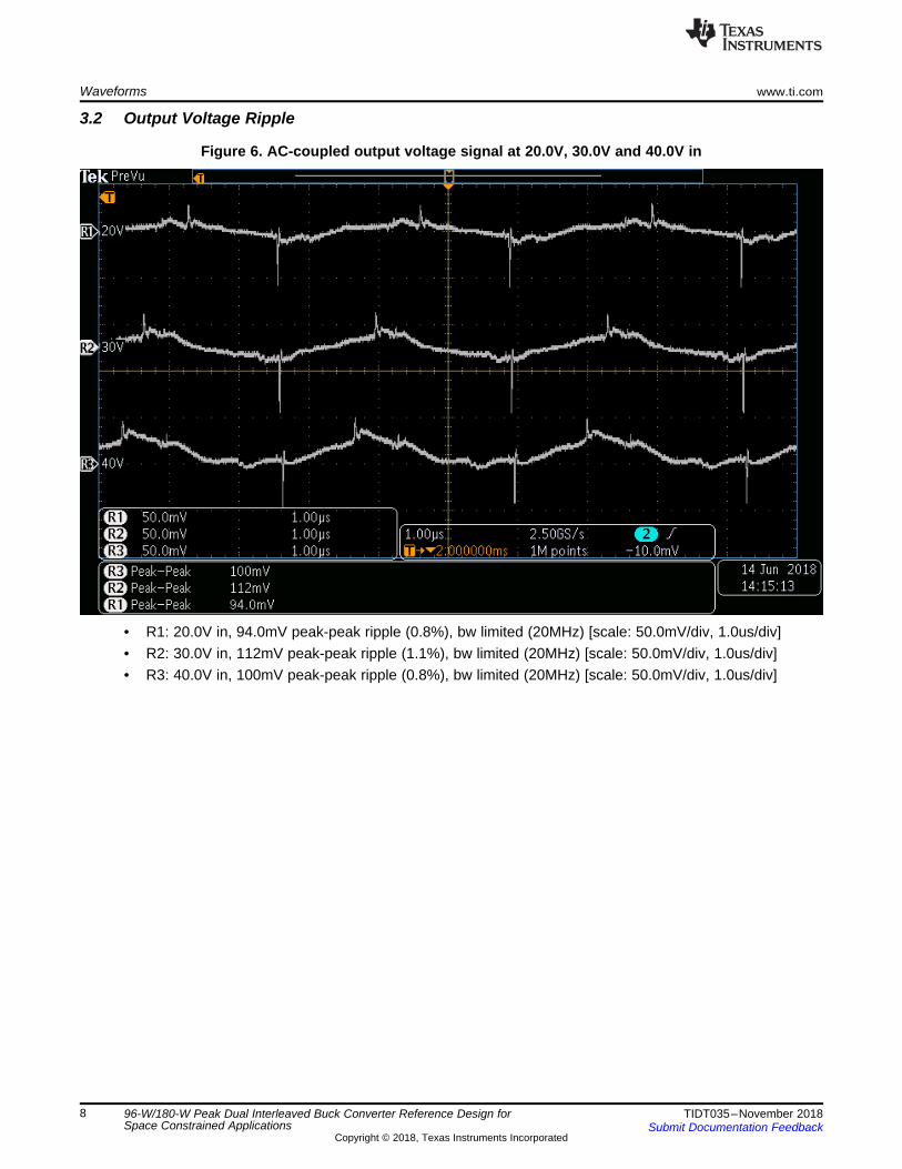
3.2 Output Voltage Ripple
Figure 6. AC-coupled output voltage signal at 20.0V, 30.0V and 40.0V in
• R1: 20.0V in, 94.0mV peak-peak ripple (0.8%), bw limited (20MHz) [scale: 50.0mV/div, 1.0us/div]• R2: 30.0V in, 112mV peak-peak ripple (1.1%), bw limited (20MHz) [scale: 50.0mV/div, 1.0us/div]• R3: 40.0V in, 100mV peak-peak ripple (0.8%), bw limited (20MHz) [scale: 50.0mV/div, 1.0us/div]
www.ti.com Waveforms
9TIDT035–November 2018Submit Documentation Feedback
Copyright © 2018, Texas Instruments Incorporated
96-W/180-W Peak Dual Interleaved Buck Converter Reference Design forSpace Constrained Applications
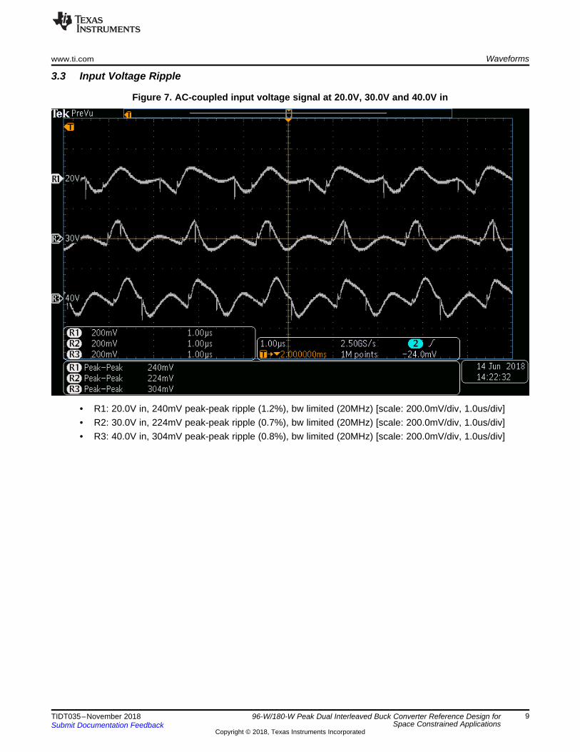
3.3 Input Voltage Ripple
Figure 7. AC-coupled input voltage signal at 20.0V, 30.0V and 40.0V in
• R1: 20.0V in, 240mV peak-peak ripple (1.2%), bw limited (20MHz) [scale: 200.0mV/div, 1.0us/div]• R2: 30.0V in, 224mV peak-peak ripple (0.7%), bw limited (20MHz) [scale: 200.0mV/div, 1.0us/div]• R3: 40.0V in, 304mV peak-peak ripple (0.8%), bw limited (20MHz) [scale: 200.0mV/div, 1.0us/div]

Waveforms www.ti.com
10 TIDT035–November 2018Submit Documentation Feedback
Copyright © 2018, Texas Instruments Incorporated
96-W/180-W Peak Dual Interleaved Buck Converter Reference Design forSpace Constrained Applications
3.4 Bode Plot
Figure 8. Bode plot at 20.0V, 30.0V and 40.0V in
• 20.0V in, 15.0A load current: fco 15.83kHz, 68deg phase margin, -30dB gain margin• 30.0V in, 15.0A load current: fco 15.53kHz, 66deg phase margin, -31dB gain margin• 40.0V in, 15.0A load current: fco 15.46kHz, 65deg phase margin, -31dB gain margin

www.ti.com Waveforms
11TIDT035–November 2018Submit Documentation Feedback
Copyright © 2018, Texas Instruments Incorporated
96-W/180-W Peak Dual Interleaved Buck Converter Reference Design forSpace Constrained Applications
3.5 Load Transients
Figure 9. Load transient from 7.5A to 15.0A at 30.0V in results in 260mV undershoot (2.2%) and 228mVovershoot (1.9%).
• Ch2: AC-coupled output voltage, bw limited (20MHz) [scale: 200mV/div, 2.0ms/div]• Ch4: output current, bw limited (20MHz) [scale: 7.5A/div, 2.0ms/div]

Waveforms www.ti.com
12 TIDT035–November 2018Submit Documentation Feedback
Copyright © 2018, Texas Instruments Incorporated
96-W/180-W Peak Dual Interleaved Buck Converter Reference Design forSpace Constrained Applications
3.6 Start-up Sequence
Figure 10. Start-up sequence at 30.0V in with no load attached.
• Ch1: output voltage [scale: 5.0V/div, 2.0ms/div]• Ch3: input voltage [scale: 20.0V/div, 2.0ms/div]

www.ti.com Waveforms
13TIDT035–November 2018Submit Documentation Feedback
Copyright © 2018, Texas Instruments Incorporated
96-W/180-W Peak Dual Interleaved Buck Converter Reference Design forSpace Constrained Applications
3.7 Undervoltage Protection
Figure 11. Undervoltage protection with a 15.0A load attached.
• Ch1: output voltage [scale: 5.0V/div, 2.0ms/div]• Ch3: input voltage [scale: 20.0V/div, 2.0ms/div]

IMPORTANT NOTICE AND DISCLAIMERTI PROVIDES TECHNICAL AND RELIABILITY DATA (INCLUDING DATASHEETS), DESIGN RESOURCES (INCLUDING REFERENCEDESIGNS), APPLICATION OR OTHER DESIGN ADVICE, WEB TOOLS, SAFETY INFORMATION, AND OTHER RESOURCES “AS IS”AND WITH ALL FAULTS, AND DISCLAIMS ALL WARRANTIES, EXPRESS AND IMPLIED, INCLUDING WITHOUT LIMITATION ANYIMPLIED WARRANTIES OF MERCHANTABILITY, FITNESS FOR A PARTICULAR PURPOSE OR NON-INFRINGEMENT OF THIRDPARTY INTELLECTUAL PROPERTY RIGHTS.These resources are intended for skilled developers designing with TI products. You are solely responsible for (1) selecting the appropriateTI products for your application, (2) designing, validating and testing your application, and (3) ensuring your application meets applicablestandards, and any other safety, security, or other requirements. These resources are subject to change without notice. TI grants youpermission to use these resources only for development of an application that uses the TI products described in the resource. Otherreproduction and display of these resources is prohibited. No license is granted to any other TI intellectual property right or to any third partyintellectual property right. TI disclaims responsibility for, and you will fully indemnify TI and its representatives against, any claims, damages,costs, losses, and liabilities arising out of your use of these resources.TI’s products are provided subject to TI’s Terms of Sale (https:www.ti.com/legal/termsofsale.html) or other applicable terms available eitheron ti.com or provided in conjunction with such TI products. TI’s provision of these resources does not expand or otherwise alter TI’sapplicable warranties or warranty disclaimers for TI products.IMPORTANT NOTICE
Mailing Address: Texas Instruments, Post Office Box 655303, Dallas, Texas 75265Copyright © 2021, Texas Instruments Incorporated