82527 SERIAL COMMUNICATIONS CONTROLLER AREA NETWORK PROTOCOL
22
82527 SERIAL COMMUNICATIONS CONTROLLER AREA NETWORK PROTOCOL Express Advance Information Datasheet Product Features ■ Supports CAN Specification 2.0 —Standard Data and Remote Frames —Extended Data and Remote Frames ■ Programmable Global Mask —Standard Message ldentifier —Extended Message ldentifier ■ 15 Message Objects of 8-Byte Data Length —14 Tx/Rx Buffers —1 Rx Buffer with Programmable Mask ■ Flexible CPU Interface —8-Bit Multiplexed —16-Bit Multiplexed —8-Bit Non-Multiplexed (Synchronous/ Asynchronous) —Serial Interface ■ Programmable Bit Rate ■ Programmable Clock Output ■ Flexible Interrupt Structure ■ Flexible Status Interface ■ Configurable Output Driver ■ Configurable Input Comparator ■ Two 8-Bit Bidirectional I/O Ports ■ 44-Lead PLCC Package ■ Pinout Compatibility with the 82526 Order No: 273150-001 December 1997 Notice: This document contains information on products in the sampling and initial production phases of development. The specifications are subject to change without notice. Verify with your local Intel sales office that you have the latest datasheet before finalizing a design.
Transcript of 82527 SERIAL COMMUNICATIONS CONTROLLER AREA NETWORK PROTOCOL

82527 SERIAL COMMUNICATIONS CONTROLLER AREA NETWORK PROTOCOLExpress
Advance Information DatasheetProduct Features
■ Supports CAN Specification 2.0—Standard Data and Remote Frames
—Extended Data and Remote Frames
■ Programmable Global Mask—Standard Message ldentifier
—Extended Message ldentifier
■ 15 Message Objects of 8-Byte Data Length—14 Tx/Rx Buffers
—1 Rx Buffer with Programmable Mask
■ Flexible CPU Interface—8-Bit Multiplexed
—16-Bit Multiplexed
—8-Bit Non-Multiplexed (Synchronous/Asynchronous)
—Serial Interface
■ Programmable Bit Rate■ Programmable Clock Output■ Flexible Interrupt Structure■ Flexible Status Interface■ Configurable Output Driver■ Configurable Input Comparator■ Two 8-Bit Bidirectional I/O Ports■ 44-Lead PLCC Package■ Pinout Compatibility with the 82526
Order No: 273150-001December 1997
Notice: This document contains information on products in the sampling and initial production phases of development. The specifications are subject to change without notice. Verify with your local Intel sales office that you have the latest datasheet before finalizing a design.
82527 - Express
ii
Information in thisproperty rights is gwhatsoever, and Infitness for a particintended for use in
Intel may make ch
Designers must nofuture definition an
The 82527 - ExpreCurrent characteri
Contact your local
Copies of docume
Intel CoPO BoxDenver call 1-80
Copyright © Intel C
*Third-party brand
Advance Information Datasheet
document is provided in connection with Intel products. No license, express or implied, by estoppel or otherwise, to any intellectual ranted by this document. Except as provided in Intel’s Terms and Conditions of Sale for such products, Intel assumes no liability tel disclaims any express or implied warranty, relating to sale and/or use of Intel products including liability or warranties relating to
ular purpose, merchantability, or infringement of any patent, copyright or other intellectual property right. Intel products are not medical, life saving, or life sustaining applications.
anges to specifications and product descriptions at any time, without notice.
t rely on the absence or characteristics of any features or instructions marked "reserved" or "undefined." Intel reserves these for d shall have no responsibility whatsoever for conflicts or incompatibilities arising from future changes to them.
ss may contain design defects or errors known as errata which may cause the product to deviate from published specifications. zed errata are available on request.
Intel sales office or your distributor to obtain the latest specifications and before placing your product order.
nts which have an ordering number and are referenced in this document, or other Intel literature, may be obtained from:
rporation 5937 CO 80217-98080-548-4725
orporation 7/8/97
s and names are the property of their respective owners.
82527 - Express
Contents
1.0 INTRODUCTION.....................................................................................................1
2.0 PIN DESCRIPTIONS .............................................................................................3
3.0 ELECTRICAL CHARACTERISTICS .................................................................5
3.1 DC CHARACTERISTICS ................................................................................ 53.2 PHYSICAL LAYER SPECIFICATIONS........................................................... 63.3 CLOCKOUT SPECIFICATIONS ..................................................................... 63.4 AC CHARACTERISTICS ................................................................................ 7
3.4.1 8/16-Bit Multiplexed Intel Modes (Modes 0, 1) ................................... 73.4.2 8-Bit Multiplexed Non-Intel Mode (Mode 2) ...................................... 103.4.3 8-Bit Non-Multiplexed Asynchronous Mode (Mode 3) ...................... 123.4.4 8-Bit Non-Multiplexed Synchronous Mode (Mode 3)........................ 143.4.5 Serial Interface Mode ....................................................................... 163.4.6 AC Testing Input............................................................................... 18
4.0 DATASHEET REVISION HISTORY................................................................18
Advance Information Datasheet iii
82527 - Express
Figures1 TN82527 Block Diagram ..................................................................................22 TN82527 44-Pin PLCC Package .....................................................................23 82527 System Timings (Modes 0, 1) ...............................................................84 Ready Output Timing for a Write Cycle if No Previous Write
is Pending (Modes 0, 1) ...................................................................................95 Ready Output Timing for Write Cycle if Previous Write Cycle
is Active (Modes 0, 1........................................................................................96 Ready Output Timing for Read Cycle (Modes 0, 1) .........................................97 82527 System Bus Timing (Mode 2) ..............................................................118 Timing of the Asynchronous Mode Read Cycle (Mode 3)..............................139 Timing of the Asynchronous Mode Write Cycle (Mode 3) ..............................1310 Timing of the Synchronous Read Cycle (Mode 3) .........................................1511 Timing of the Synchronous Write Cycle (Mode 3)..........................................1512 Serial Interface Mode (Priority = 0, Phase = 0) ..............................................1713 Serial Interface Mode (Priority = 1, Phase = 1) ..............................................17
Tables1 Pin Type Legend ..............................................................................................32 Pin Descriptions ...............................................................................................33 DC Characteristics ...........................................................................................54 DC Characteristics ...........................................................................................65 Clockout Specifications ....................................................................................66 AC Characteristics 8/16-Bit Multiplexed Intel Modes (Modes 0, 1) ..................77 AC Characteristics 8-Bit Multiplexed Non-Intel Mode (Mode 2) .....................108 AC Characteristics 8-Bit Non-Multiplexed Asynchronous Mode (Mode 3) .....129 AC Characteristics 8-Bit Non-Multiplexed Synchronous Mode (Mode 3).......1410 AC Characteristics for Serial Interface Mode .................................................16
iv Advance Information Datasheet
82527 - Express
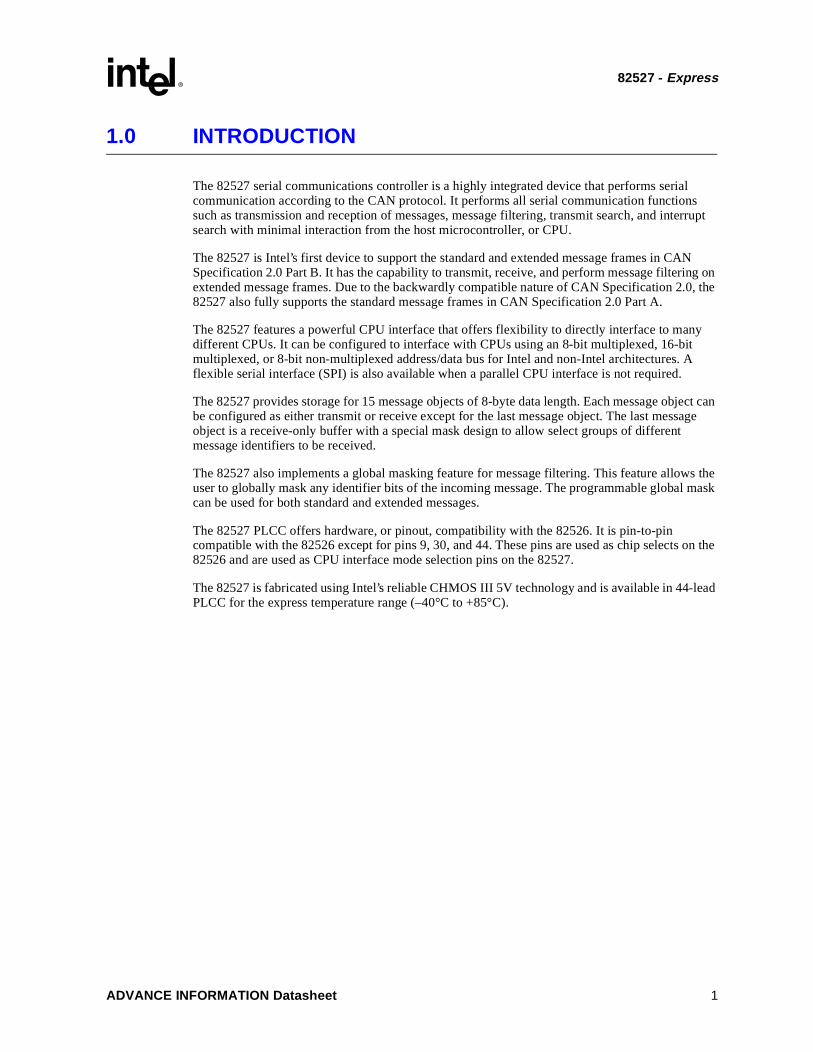
1.0 INTRODUCTION
The 82527 serial communications controller is a highly integrated device that performs serial communication according to the CAN protocol. It performs all serial communication functions such as transmission and reception of messages, message filtering, transmit search, and interrupt search with minimal interaction from the host microcontroller, or CPU.
The 82527 is Intel’s first device to support the standard and extended message frames in CAN Specification 2.0 Part B. It has the capability to transmit, receive, and perform message filtering on extended message frames. Due to the backwardly compatible nature of CAN Specification 2.0, the 82527 also fully supports the standard message frames in CAN Specification 2.0 Part A.
The 82527 features a powerful CPU interface that offers flexibility to directly interface to many different CPUs. It can be configured to interface with CPUs using an 8-bit multiplexed, 16-bit multiplexed, or 8-bit non-multiplexed address/data bus for Intel and non-Intel architectures. A flexible serial interface (SPI) is also available when a parallel CPU interface is not required.
The 82527 provides storage for 15 message objects of 8-byte data length. Each message object can be configured as either transmit or receive except for the last message object. The last message object is a receive-only buffer with a special mask design to allow select groups of different message identifiers to be received.
The 82527 also implements a global masking feature for message filtering. This feature allows the user to globally mask any identifier bits of the incoming message. The programmable global mask can be used for both standard and extended messages.
The 82527 PLCC offers hardware, or pinout, compatibility with the 82526. It is pin-to-pin compatible with the 82526 except for pins 9, 30, and 44. These pins are used as chip selects on the 82526 and are used as CPU interface mode selection pins on the 82527.
The 82527 is fabricated using Intel’s reliable CHMOS III 5V technology and is available in 44-lead PLCC for the express temperature range (–40°C to +85°C).
ADVANCE INFORMATION Datasheet 1
82527 - Express
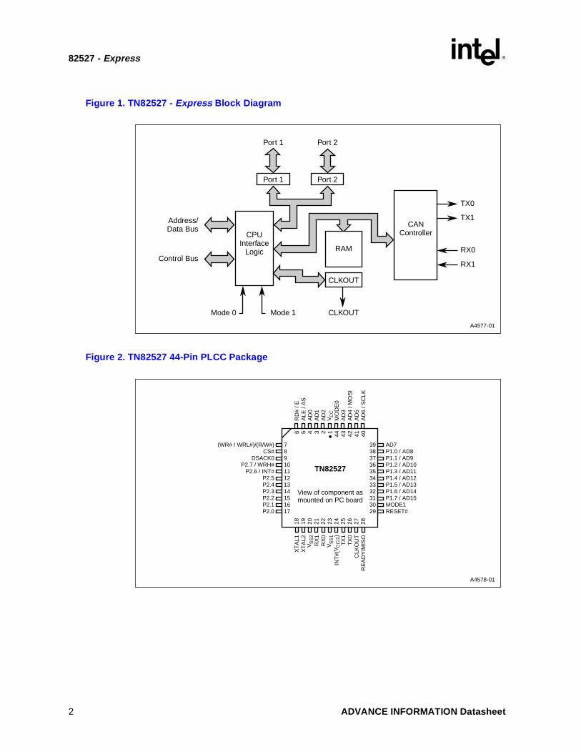
Figure 1. TN82527 - Express Block Diagram
Figure 2. TN82527 44-Pin PLCC Package
A4577-01
CPU Interface
Logic
CAN Controller
CLKOUT
CLKOUTMode 1
TX1
TX0
RAM
Port 2Port 1
Port 2Port 1
RX1
RX0
Mode 0
Address/ Data Bus
Control Bus
A4578-01
AD7 P1.0 / AD8 P1.1 / AD9 P1.2 / AD10 P1.3 / AD11 P1.4 / AD12 P1.5 / AD13 P1.6 / AD14 P1.7 / AD15 MODE1 RESET#
RD
# / E
A
LE /
AS
A
D0
AD
1 A
D2
VC
C
MO
DE
0 A
D3
AD
4 / M
OS
I A
D5
AD
6 / S
CLK
(WR# / WRL#)/(R/W#) CS#
DSACK0 P2.7 / WRH#
P2.6 / INT# P2.5 P2.4 P2.3 P2.2 P2.1 P2.0
39 38 37 36 35 34 33 32 31 30 29
TN82527
View of component as mounted on PC board
7 8 9 10 11 12 13 14 15 16 17
XT
AL1
X
TA
L2
VS
S2
RX
1 R
X0
VS
S1
INT
#(V
CC
/2)
TX
1 T
X0
CLK
OU
T
RE
AD
Y/M
ISO
18
19
20
21
22
23
24
25
26
27
28
6 5 4 3 2 1 44
43
42
41
40
2 ADVANCE INFORMATION Datasheet
82527 - Express
2.0 PIN DESCRIPTIONS
The 82527 - Express pins are described in this section. Table 1 presents the legend for interpreting the pin types.
Table 1. Pin Type Legend
Symbol Description
I Input Only Pin
O Output Only Pin
I/O Pin can be either Input or Output
Table 2. Pin Descriptions (Sheet 1 of 2)
Name Type Description
VSS1 Ground GROUND connection must be connected externally to a VSS board plane. Provides digital ground.
VSS2 Ground GROUND connection must be connected externally to a VSS board plane. Provides ground for analog comparator.
VCC Power POWER connection must be connected externally to +5 V DC. Provides power for entire device.
XTAL1 I Input for an external clock. XTAL1 (along with XTAL2) are the crystal connections to an internal oscillator.
XTAL2 O
Push-pull output from the internal oscillator. XTAL2 (along with XTAL1) are the crystal connections to an internal oscillator. If an external oscillator is used, XTAL2 must be floated, or not be connected. XTAL2 must not be used as a clock output to drive other CPUs.
CLKOUT O Programmable clock output. This output may be used to drive the oscillator of the host microcontroller.
RESET# I
Warm Reset: (VCC remains valid while RESET# is asserted), RESET# must be driven to a valid low level for 1 ms minimum.
Cold Reset: (VCC is driven to a valid level while RESET# is asserted), RESET# must be driven low for 1 ms minimum measured from a valid VCC level. No falling edge on the reset pin is required during a cold reset event.
CS## I A low level on this pin enables CPU access to the 82527 device.
INT#
(VCC/2)
O
O
The interrupt pin is an open-drain output to the host microcontroller. VCC/2 is the power supply for the ISO low speed physical layer. The function of this pin is determined by the MUX bit in the CPU Interface Register (Address 02H) as follows:
MUX e 1: pin 24 (PLCC) = VCC/2, pin 11 = INT#
MUX e 0: pin 24 (PLCC) = INT#
RX0
RX1
I
I
Inputs from the CAN bus line(s) to the input comparator. A recessive level is read when RX0 > RX1. A dominant level is read when RX1 > RX0. When the CoBy bit (Bus Configuration register) is programmed as a “1”, the input comparator is bypassed and RX0 is the CAN bus line input.
TX0
TX1
O
OSerial data push-pull output to the CAN bus line. During a recessive bit TX0 is high and TX1 is low. During a dominant bit TX0 is low and TX1 is high.
ADVANCE INFORMATION Datasheet 3
82527 - Express
AD0/A0/ICPAD1/A1/CPAD2/A2/CSASAD3/A3/STEAD4/A4/MOSIAD5/A5AD6/A6/SCLKAD7/A7
I/O-I-II/O-I-II/O-I-II/O-I
I/O-I-II/O-I
I/O-I-II/O-I
Address/Data bus in 8-bit multiplexed mode.
Address bus in 8-bit non-multiplexed mode.
Low byte of A/D bus in 16-bit multiplexed mode.
In Serial Interface mode, the following pins have the following meaning:
AD0: ICP Idle Clock PolarityAD1: CP Clock PhaseAD2: CSAS Chip Select Active StateAD3: STE Sync Transmit EnableAD6: SCLK Serial Clock InputAD4: MOSI Serial Data Input
AD8/D0/P1.0AD9/D1/P1.1AD10/D2/P1.2AD11/D3/P1.3AD12/D4/P1.4AD13/D5/P1.5AD14/D6/P1.6AD15/D7/P1.7
I/O-O-I/OI/O-O-I/OI/O-O-I/OI/O-O-I/OI/O-O-I/OI/O-O-I/OI/O-O-I/OI/O-O-I/O
High byte of A/D bus in 16-bit multiplexed mode.
Data bus in 8-bit non-multiplexed mode.
Low speed I/O port. P1 pins in 8-bit multiplexed mode and serial mode.
Port pins have weak pullups until the port is configured by writing to 9FH and AFH.
P2.0P2.1P2.2P2.3P2.4P2.5P2.6/INT#P2.7/WRH#
I/OI/OI/OI/OI/OI/O
I/O-OI/O-I
P2 in all modes.
P2.6 is INT# when MUX = 1 and is open-drain.
P2.7 is WRH# in 16-bit multiplexed mode.
Mode0Mode1
II
These pins select one of the four parallel interfaces. These pins are weakly held low during reset.
Mode1 Mode0
0 0 8-bit multiplexed — Intel0 0 Serial Interface mode entered when RD# = 0,
WR# = 0 upon reset.0 1 16-bit multiplexed — Intel1 0 8-bit multiplexed — non-Intel1 1 8-bit non-multiplexed
ALE/AS I-IALE used for Intel modes.
AS used for non-Intel modes, except Mode 3 this pin must be tied high.
RD#E
II
RD#used for Intel modes.
E used for non-Intel modes, except Mode 3 Asynchronous this pin must be tied high.
WR#/WRL#R/W#
II
WR#in 8-bit Intel mode and WRL# in 16-bit Intel mode.
R/W# used for non-Intel modes.
READYMISO
OO
READY is an output to synchronize accesses from the host microcontroller to the 82527. READY is an open-drain output to the host microcontroller. MISO is the serial data output for the serial interface mode.
DSACK0# O DSACK0# is an open-drain output to synchronize accesses from the host microcontroller to the 82527.
Table 2. Pin Descriptions (Sheet 2 of 2)
Name Type Description
4 ADVANCE INFORMATION Datasheet
82527 - Express
3.0 ELECTRICAL CHARACTERISTICS
3.1 DC CHARACTERISTICS
Operating Conditions:
• VCC = 5 V ±10%
• TA = –40°C to +85°C
ABSOLUTE MAXIMUM RATINGS*
Storage Temperature –60°C to +150°C
Voltage from Any Pin toVSS ................................................. –0.5 V to +7.0 V
Laboratory testing shows the 82527 will withstand up to 10 mA of injected current into both RX0 and RX1 pins for a total of 20 days without sustaining permanent damage. This high current condition may be the result of shorted signal lines. The 82527 will not function properly if the RX0/RX1 input voltage exceeds VCC+0.5 V.
NOTICE: This is a production data sheet. The specifi-cations are subject to change without notice. Verify with your local Intel sales office that you have the latest datasheet before finalizing a design.
*WARNING: Stressing the device beyond the “Absolute Maximum Ratings” may cause permanent damage. These are stress ratings only. Operation beyond the “Operating Conditions” is not recommended and extended exposure beyond the “Operating Conditions” may affect device reliability.
Table 3. DC Characteristics
Sym Parameter Min Max Conditions
VILInput Low Voltage (All except RX0, RX1, AD0±AD7 in Mode 3) –0.5 0.8 V
VIL1 Input Low Voltage for AD00–D7 in Mode 3 –0.5 0.5 V
VIL2Input Low Voltage (RX0) for Comparator Bypass Mode 0.5 V
VIL3Input Low Voltage for Port 1 and Port 2 Pins Not Used for Interface to Host CPU 0.3 VCC
VIH Input High Voltage (All except RX0, RX1, RESET#) 3.0 V VCC + 0.5 V
VIH1Input High Voltage (RESET#) Hysteresis on RESET#
3.0 V200 mV VCC + 0.5 V
VIH2Input High Voltage (RX0) for Comparator Bypass Mode 4.0 V
VIH3Input High Voltage for Port 1 and Port 2 Pins Not Used for Interface to Host CPU 0.7 VCC
VOL Output Low Voltage (All Outputs except TX0, TX1) 0.45 V IOL = 1.6 mA
VOHOutput High Voltage (All Outputs except TX0, TX1, CLOCKOUT) VCC – 0.8 V IOH = –200 µA
VOHR1 Output High Voltage (CLOCKOUT) 0.8 V IOH = –80 µA
ILK Input Leakage Current ±10 µA VSS < VIN < VCC
CIN PIN Capacitance** 10 pF FXTAL = 1 KHz
ICC Supply Current 50 mA FXTAL = 16 KHz(1)
ISLEEP
Sleep Currentwith VCC/2 Output Enabled, No Loadwith VCC/2 Output Disabled
700 µA100 µA
(1)
IPD Powerdown Current 25 µA XTAL1 Clocked(1)
NOTES:**Typical value based on characterization data. Port pins are weakly held after reset until the port
configuration registers are written (9FH, AFH).1. All pins are driven to VSS or VCC including RX0 and RX1.
ADVANCE INFORMATION Datasheet 5

82527 - Express
3.2 PHYSICAL LAYER SPECIFICATIONS
Operating Conditions:
• Load = 100 pF
• VCC = 5 V ±10%
• TA = –40°C to +85°C
3.3 CLOCKOUT SPECIFICATIONS
Operating Conditions:
• Load = 50 pF
Table 4. DC Characteristics
RX0/RX1 and TX0/TX1 Min Max Conditions
Input Voltage –0.5 V VCC + 0.5 V
Common Mode Range VSS + 1 V VCC – 1 V
Differential Input Threshold ±100 mV
Internal Delay 1: Sum of the Comparator Input Delay and the TX0/TX1 Output Driver Delay
60 nsLoad on TX0, TX1 = 100 pF, +100 mV to –100 mV RX0/RX1 differential
Internal Delay 2: Sum of the RX0 Pin Delay (if the Comparator is Bypassed) and the TX0/TX1 Output Driver Delay
50 ns Load on TX0, TX1 = 100 pF
Source Current on Each TX0, TX1 –10 mA VOUT = VCC – 1 V
Sink Current on Each TX0, TX1 10 mA VOUT = 1 V
Input Hysteresis for RX0/RX12 0 V
VCC/2
VCC/2 2.38 V 2.62 V IOUT ≤ 75 µA, VCC = 5 V
Table 5. Clockout Specifications
Parameter Min Max
CLOCKOUT Frequency XTAL/15 XTAL
6 ADVANCE INFORMATION Datasheet
82527 - Express
3.4 AC CHARACTERISTICS
3.4.1 8/16-Bit Multiplexed Intel Modes (Modes 0, 1)
Operating Conditions:
• VCC = 5 V ±10% • VSS = 0 V • TA = –40°C to +85ºC • CL = 100 pF
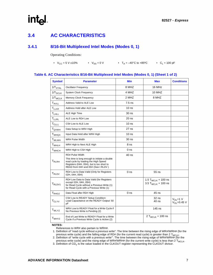
Table 6. AC Characteristics 8/16-Bit Multiplexed Intel Modes (Modes 0, 1) (Sheet 1 of 2)
Symbol Parameter Min Max Conditions
1/TXTAL Oscillator Frequency 8 MHZ 16 MHz
1/TSCLK System Clock Frequency 4 MHZ 10 MHZ
1/TMCLK Memory Clock Frequency 2 MHZ 8 MHZ
TAVLL Address Valid to ALE Low 7.5 ns
TLLAX Address Hold after ALE Low 10 ns
TLHLL ALE High Time 30 ns
TLLRL ALE Low to RD# Low 20 ns
TCLLL CS# Low to ALE Low 10 ns
TQVWH Data Setup to WR# High 27 ns
TWHQX Input Data Hold after WR# High 10 ns
TWLWH WR# Pulse Width 30 ns
TWHLH WR# High to Next ALE High 8 ns
TWHCH WR# High to CS# High 0 ns
TRLRH
RD# Pulse Width
This time is long enough to initiate a double read cycle by loading the High Speed Registers (04H, 05H), but is too short to READ from 04H and 05H (See t RLDV )
40 ns
TRLDVRD# Low to Data Valid (Only for Registers 02H, 04H, 05H)
0 ns 55 ns
TRLDV1
RD# Low Data to Data Valid (for Registers except 02H, 04H, 05H)for Read Cycle without a Previous Write (1)for Read Cycle with a Previous Write (1)
1.5 TMCLK + 100 ns3.5 TMCLK + 100 ns
TRHDZ Data Float after RD# High 0 ns 45 ns
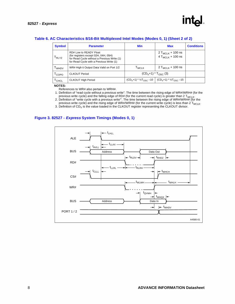
TCLYV
CS# Low to READY Setup Condition:Load Capacitance on the READY Output: 50 pF
32 ns40 ns
VOL=1 VVOL=0.45 V
TWLYZWR# Low to READY Float for a Write Cycle if No Previous Write is Pending (2)
145 ns
TWHYZEnd of Last Write to READY Float for a Write Cycle if a Previous Write Cycle is Active (2)
2 TMCLK + 100 ns
NOTES:References to WR# also pertain to WRH#.
1. Definition of “read cycle without a previous write”: The time between the rising edge of WR#/WRH# (for the previous write cycle) and the falling edge of RD# (for the current read cycle) is greater than 2 TMCLK.
2. Definition of “write cycle with a previous write'”. The time between the rising edge of WR#/WRH# (for the previous write cycle) and the rising edge of WR#/WRH# (for the current write cycle) is less than 2 TMCLK.
3. Definition of CDV is the value loaded in the CLKOUT register representing the CLKOUT divisor.
ADVANCE INFORMATION Datasheet 7
82527 - Express
TRLYZ
RD# Low to READY Float(for registers except 02H, 04H, 05H)for Read Cycle without a Previous Write (1)for Read Cycle with a Previous Write (1)
2 TMCLK + 100 ns4 TMCLK + 100 ns
TWHDV WR# High ti Output Data Valid on Port 1/2 TMCLK 2 TMCLK + 100 ns
TCOPO CLKOUT Period (CDV+1) * TOSC (3)
TCHCL CLKOUT High Period (CDV+1) * ½TOSC –10 (CDV+1) * ½TOSC –15
Figure 3. 82527 - Express System Timings (Modes 0, 1)
Table 6. AC Characteristics 8/16-Bit Multiplexed Intel Modes (Modes 0, 1) (Sheet 2 of 2)
Symbol Parameter Min Max Conditions
NOTES:References to WR# also pertain to WRH#.
1. Definition of “read cycle without a previous write”: The time between the rising edge of WR#/WRH# (for the previous write cycle) and the falling edge of RD# (for the current read cycle) is greater than 2 TMCLK.
2. Definition of “write cycle with a previous write'”. The time between the rising edge of WR#/WRH# (for the previous write cycle) and the rising edge of WR#/WRH# (for the current write cycle) is less than 2 TMCLK.
3. Definition of CDV is the value loaded in the CLKOUT register representing the CLKOUT divisor.
A4580-01
ALE
CS#
WR#
BUS
RD#
tLHLL
tAVLL
tCLLL
tLLAX
tLLRL tRLRHtWHCH
tRLDV tRHDZ
tWHLH
tWHQX
tWHDV
tQVWH
tWLWH
Address Data Out
BUS Address
PORT 1 / 2
Data In
8 ADVANCE INFORMATION Datasheet
82527 - Express
Figure 4. Ready Output Timing for a Write Cycle if No Previous Write is Pending (Modes 0, 1)
Figure 5. Ready Output Timing for Write Cycle if Previous Write Cycle is Active (Modes 0, 1)
Figure 6. Ready Output Timing for Read Cycle (Modes 0, 1)
CS#
WR#
ReadytCLYV tWLYZ
CS#
WR#
Ready
tWHYZ
tCLYV
CS#
ALE
RD#
Ready
tRLYZ
ADVANCE INFORMATION Datasheet 9
82527 - Express
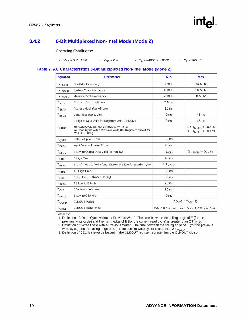
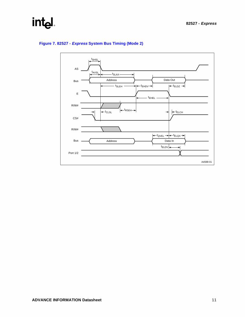
3.4.2 8-Bit Multiplexed Non-Intel Mode (Mode 2)
Operating Conditions::
• VCC = 5 V ±10% • VSS = 0 V • TA = –40°C to +85ºC • CL = 100 pF
Table 7. AC Characteristics 8-Bit Multiplexed Non-Intel Mode (Mode 2)
Symbol Parameter Min Max
1/TXTAL Oscillator Frequency 8 MHZ 16 MHz
1/TSCLK System Clock Frequency 4 MHZ 10 MHZ
1/TMCLK Memory Clock Frequency 2 MHZ 8 MHZ
TAVLL Address Valid to AS Low 7.5 ns
TSLAX Address Hold after AS Low 10 ns
TELDZ Data Float after E Low 0 ns 45 ns
TEHDV
E High to Data Valid for Registers 02H, 04H, 05H 0 ns 45 ns
for Read Cycle without a Previous Write (1)for Read Cycle with a Previous Write (for Registers except for 02H, 04H, 05H)
1.5 TMCLK + 100 ns3.5 TMCLK + 100 ns
TQVEL Data Setup to E Low 30 ns
TELQX Input Data Hold after E Low 20 ns
TELDV E Low to Output Data Valid on Port 1/2 TMCLK 2 TMCLK + 500 ns
TEHEL E High Time 45 ns
TELEL End of Previous Write (Last E Low) to E Low for a Write Cycle 2 TMCLK
TSHSL AS High Time 30 ns
TRSEH Setup Time of R/W# to E High 30 ns
TSLEH AS Low to E High 20 ns
TCLSL CS# Low to AS Low 20 ns
TELCH E Low to CS# High 0 ns
TCOPD CLKOUT Period (CDV+1) * TOSC (3)
TCHCL CLKOUT High Period (CDV+1) * ½TOSC – 10 (CDV+1) * ½TOSC + 15
NOTES:1. Definition of “Read Cycle without a Previous Write”: The time between the falling edge of E (for the
previous write cycle) and the rising edge of E (for the current read cycle) is greater than 2 TMCLK.2. Definition of “Write Cycle with a Previous Write'”. The time between the falling edge of E (for the previous
write cycle) and the falling edge of E (for the current write cycle) is less than 2 TMCLK.3. Definition of CDV is the value loaded in the CLKOUT register representing the CLKOUT divisor.
10 ADVANCE INFORMATION Datasheet
82527 - Express
Figure 7. 82527 - Express System Bus Timing (Mode 2)
A4588-01
tEHDV
AS
Bus
E
R/W#
R/W#
tSHSL
tELDZ
tAVSL
tSLEH
Address Data Out
CS#
Bus
Port 1/2
tRSEH
tEHEL
tELDV
tELQXtQVEL
tELCHtCLSL
tSLAX
Address Data In
ADVANCE INFORMATION Datasheet 11
82527 - Express
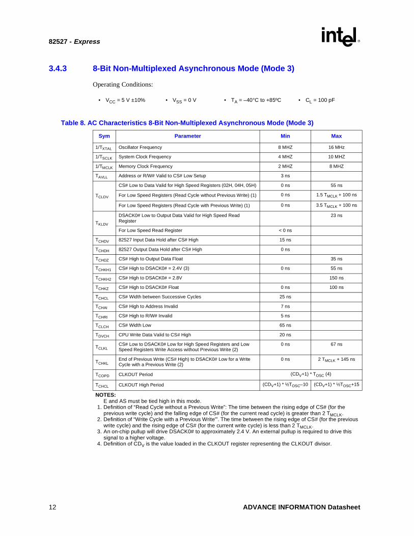
3.4.3 8-Bit Non-Multiplexed Asynchronous Mode (Mode 3)
Operating Conditions:
• VCC = 5 V ±10% • VSS = 0 V • TA = –40°C to +85ºC • CL = 100 pF
Table 8. AC Characteristics 8-Bit Non-Multiplexed Asynchronous Mode (Mode 3)
Sym Parameter Min Max
1/TXTAL Oscillator Frequency 8 MHZ 16 MHz
1/TSCLK System Clock Frequency 4 MHZ 10 MHZ
1/TMCLK Memory Clock Frequency 2 MHZ 8 MHZ
TAVLL Address or R/W# Valid to CS# Low Setup 3 ns
TCLDV
CS# Low to Data Valid for High Speed Registers (02H, 04H, 05H) 0 ns 55 ns
For Low Speed Registers (Read Cycle without Previous Write) (1) 0 ns 1.5 TMCLK + 100 ns
For Low Speed Registers (Read Cycle with Previous Write) (1) 0 ns 3.5 TMCLK + 100 ns
TKLDV
DSACK0# Low to Output Data Valid for High Speed Read Register
23 ns
For Low Speed Read Register < 0 ns
TCHDV 82527 Input Data Hold after CS# High 15 ns
TCHDH 82527 Output Data Hold after CS# High 0 ns
TCHDZ CS# High to Output Data Float 35 ns
TCHKH1 CS# High to DSACK0# = 2.4V (3) 0 ns 55 ns
TCHKH2 CS# High to DSACK0# = 2.8V 150 ns
TCHKZ CS# High to DSACK0# Float 0 ns 100 ns
TCHCL CS# Width between Successive Cycles 25 ns
TCHAI CS# High to Address Invalid 7 ns
TCHRI CS# High to R/W# Invalid 5 ns
TCLCH CS# Width Low 65 ns
TDVCH CPU Write Data Valid to CS# High 20 ns
TCLKLCS# Low to DSACK0# Low for High Speed Registers and Low Speed Registers Write Access without Previous Write (2)
0 ns 67 ns
TCHKLEnd of Previous Write (CS# High) to DSACK0# Low for a Write Cycle with a Previous Write (2)
0 ns 2 TMCLK + 145 ns
TCOPD CLKOUT Period (CDV+1) * TOSC (4)
TCHCL CLKOUT High Period (CDV+1) * ½TOSC–10 (CDV+1) * ½TOSC+15
NOTES:E and AS must be tied high in this mode.
1. Definition of “Read Cycle without a Previous Write”: The time between the rising edge of CS# (for the previous write cycle) and the falling edge of CS# (for the current read cycle) is greater than 2 TMCLK.
2. Definition of “Write Cycle with a Previous Write'”. The time between the rising edge of CS# (for the previous write cycle) and the rising edge of CS# (for the current write cycle) is less than 2 TMCLK.
3. An on-chip pullup will drive DSACK0# to approximately 2.4 V. An external pullup is required to drive this signal to a higher voltage.
4. Definition of CDV is the value loaded in the CLKOUT register representing the CLKOUT divisor.
12 ADVANCE INFORMATION Datasheet
82527 - Express
Figure 8. Timing of the Asynchronous Mode Read Cycle (Mode 3)
Figure 9. Timing of the Asynchronous Mode Write Cycle (Mode 3)
A4589-01
Address
R/W#
tCHAI
CS#
Data
DSACK0#
tAVCL
tCHDH
tCHKZtCHKH
tCHDZtCLDV
tKLDV
tCHCL
tCLKL
tCLCH
A4590-01
Address
R/W#
tCHAI
CS#
Data
DSACK0#
tAVCL
tCHKZtCHKH
tCHDVtDVCH
tCHCL
tCLKL
tCLCH
ADVANCE INFORMATION Datasheet 13
82527 - Express
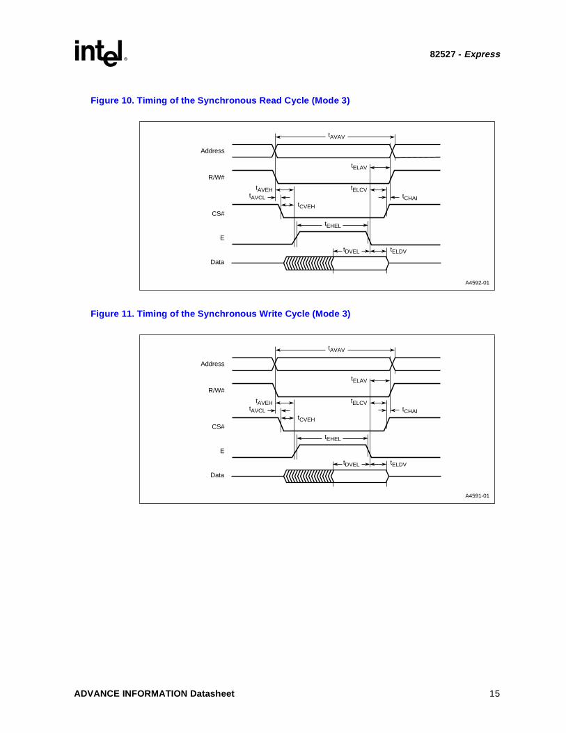
3.4.4 8-Bit Non-Multiplexed Synchronous Mode (Mode 3)
Operating Conditions:
• VCC = 5 V ±10% • VSS = 0 V • TA = –40°C to +85ºC • CL = 100 pF
Table 9. AC Characteristics 8-Bit Non-Multiplexed Synchronous Mode (Mode 3)
Sym Parameter Min Max
1/TXTAL Oscillator Frequency 8 MHZ 16 MHz
1/TSCLK System Clock Frequency 4 MHZ 10 MHZ
1/TMCLK Memory Clock Frequency 2 MHZ 8 MHZ
TEHDV
E High to Data Valid out of High Speed Register (02H, 04H, 05H) 55 ns
Read Cycle without Previous Write for Low Speed Registers(1) 1.5 TMCLK + 100 ns
Read Cycle with Previous Write for Low Speed Registers(1) 3.5 TMCLK + 100 ns
TELDH Data Hold after E Low for a Read Cycle 5 ns
TELDZ Data Float after E Low 35 ns
TELDV Data Hold after E Low for a Write Cycle 15 ns
TAVEH Address and R/W# to E Setup 25 ns
TELAV Address and R/W# Valid after E Falls 15 ns
TCVEH CS# Valid to E High 0 ns
TELCV CS# Valid after E Low 0 ns
TDVEL Data Setup to E Low 55 ns
TEHEL E Active Width 100 ns
TAVAV Start of a Write Cycle after a Previous Write Access 2 TMCLK
TAVCL Address or R/W# to CS# Low Setup 3 ns
TCHAI CS# High to Address Invalid 7 ns
TCOPD CLKOUT Period (CDV+1) * TOSC (2)
TCHCL CLKOUT High Period (CDV+1) * ½TOSC–10 (CDV+1) * ½TOSC+15
NOTES:1. Definition of “Read Cycle without a Previous Write”: The time between the falling edge of E (for the previous
write cycle) and the rising edge of E (for the current read cycle) is greater than 2 TMCLK.2. Definition of CDV is the value loaded in the CLKOUT register representing the CLKOUT divisor.
14 ADVANCE INFORMATION Datasheet
82527 - Express
Figure 10. Timing of the Synchronous Read Cycle (Mode 3)
Figure 11. Timing of the Synchronous Write Cycle (Mode 3)
A4592-01
Address
R/W#
tELAV
CS#
E
tAVEH tELCV
tDVEL tELDV
tEHEL
tCHAItAVCLtCVEH
tAVAV
Data
A4591-01
Address
R/W#
tELAV
CS#
E
tAVEH tELCV
tDVEL tELDV
tEHEL
tCHAItAVCLtCVEH
tAVAV
Data
ADVANCE INFORMATION Datasheet 15
82527 - Express
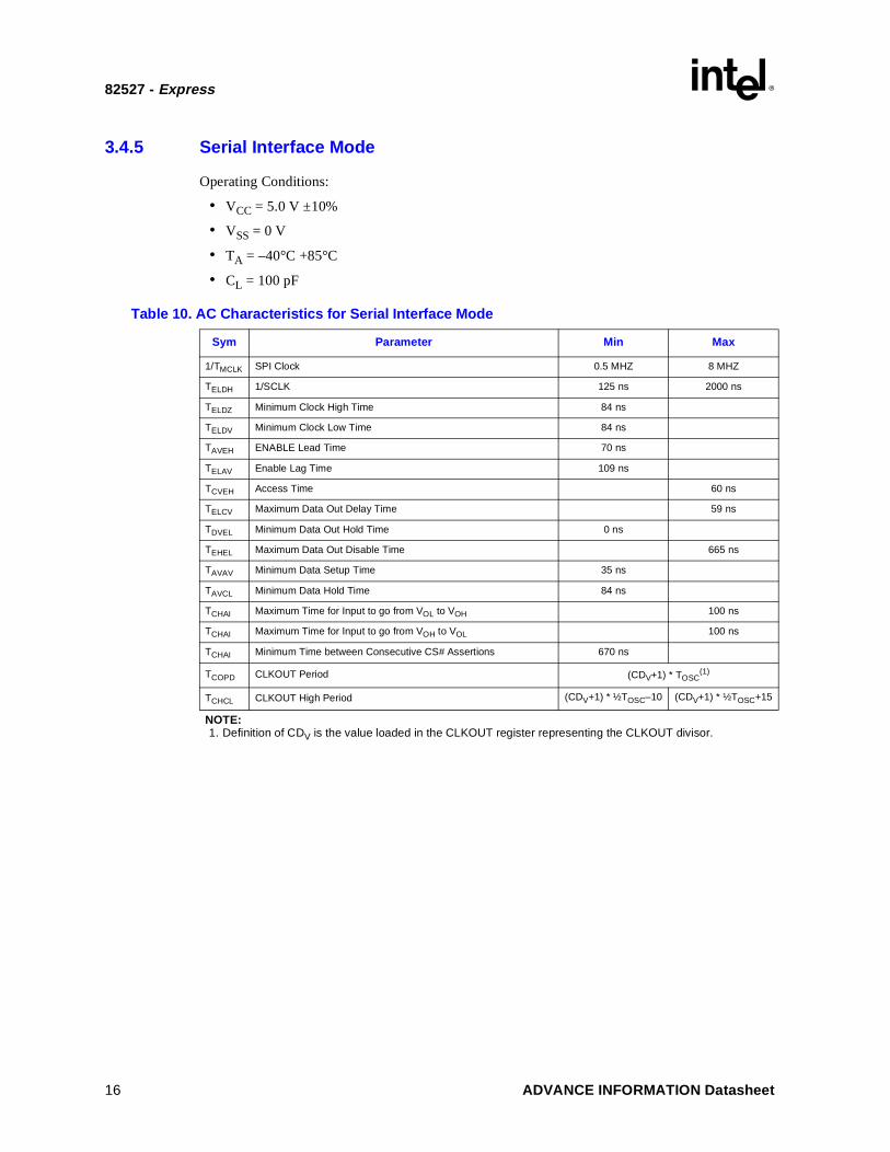
3.4.5 Serial Interface Mode
Operating Conditions:
• VCC = 5.0 V ±10%
• VSS = 0 V
• TA = –40°C +85°C
• CL = 100 pF
Table 10. AC Characteristics for Serial Interface Mode
Sym Parameter Min Max
1/TMCLK SPI Clock 0.5 MHZ 8 MHZ
TELDH 1/SCLK 125 ns 2000 ns
TELDZ Minimum Clock High Time 84 ns
TELDV Minimum Clock Low Time 84 ns
TAVEH ENABLE Lead Time 70 ns
TELAV Enable Lag Time 109 ns
TCVEH Access Time 60 ns
TELCV Maximum Data Out Delay Time 59 ns
TDVEL Minimum Data Out Hold Time 0 ns
TEHEL Maximum Data Out Disable Time 665 ns
TAVAV Minimum Data Setup Time 35 ns
TAVCL Minimum Data Hold Time 84 ns
TCHAI Maximum Time for Input to go from VOL to VOH 100 ns
TCHAI Maximum Time for Input to go from VOH to VOL 100 ns
TCHAI Minimum Time between Consecutive CS# Assertions 670 ns
TCOPD CLKOUT Period (CDV+1) * TOSC(1)
TCHCL CLKOUT High Period (CDV+1) * ½TOSC–10 (CDV+1) * ½TOSC+15
NOTE:1. Definition of CDV is the value loaded in the CLKOUT register representing the CLKOUT divisor.
16 ADVANCE INFORMATION Datasheet
82527 - Express
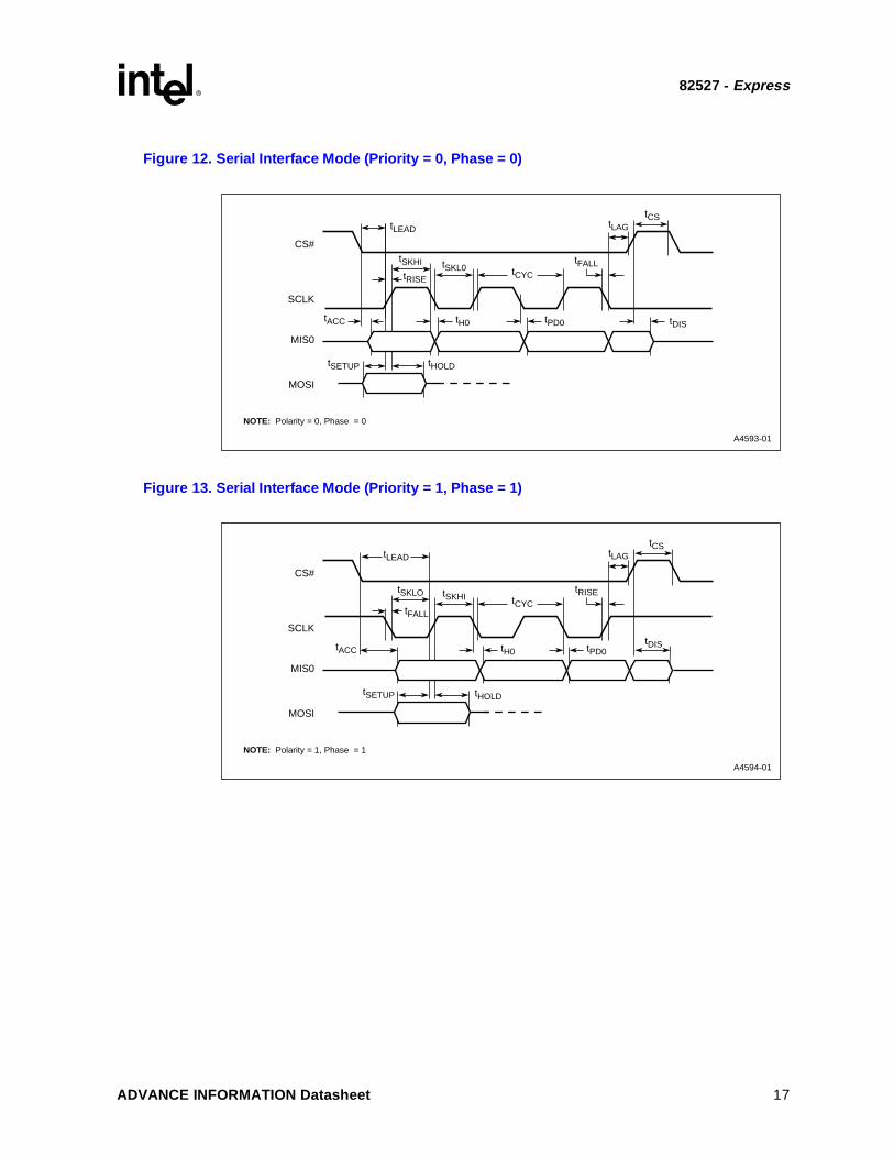
Figure 12. Serial Interface Mode (Priority = 0, Phase = 0)
Figure 13. Serial Interface Mode (Priority = 1, Phase = 1)
A4593-01
SCLK
CS#
MIS0
MOSI
tDIS
tLEAD
tPD0tH0
tCStLAG
tFALLtCYC
tSKL0tSKHI
tRISE
tSETUP
tACC
tHOLD
NOTE: Polarity = 0, Phase = 0
A4594-01
SCLK
CS#
MIS0
MOSI
tDIS
tLEAD
tPD0tH0
tCStLAG
tRISEtCYC
tSKHItSKLO
tFALL
tSETUP
tACC
tHOLD
NOTE: Polarity = 1, Phase = 1
ADVANCE INFORMATION Datasheet 17
82527 - Express
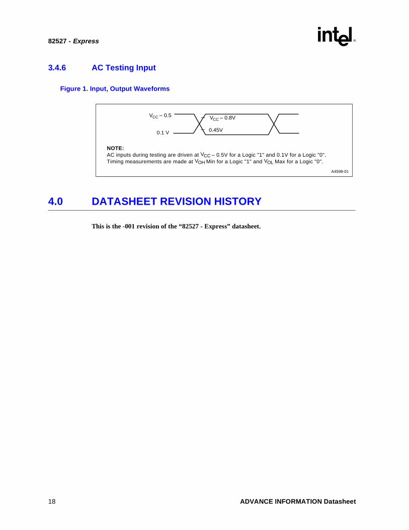
3.4.6 AC Testing Input
4.0 DATASHEET REVISION HISTORY
This is the -001 revision of the “82527 - Express” datasheet.
Figure 1. Input, Output Waveforms
A4598-01
NOTE: AC inputs during testing are driven at VCC – 0.5V for a Logic "1" and 0.1V for a Logic "0". Timing measurements are made at VOH Min for a Logic "1" and VOL Max for a Logic "0".
0.1 V
VCC – 0.5 VCC – 0.8V
0.45V
18 ADVANCE INFORMATION Datasheet